Embed Size (px)
Citation preview

Th. Detzel, O. Häberlen, A. Bricconi, A. Charles, G. Deboy, T. McDonaldInfineon Technologies Austria AG
High-Voltage (600 V) GaN Power Devices:Status and BenefitsPower Electronics Conference 2017Munich Airport Hilton, December 05, 2017
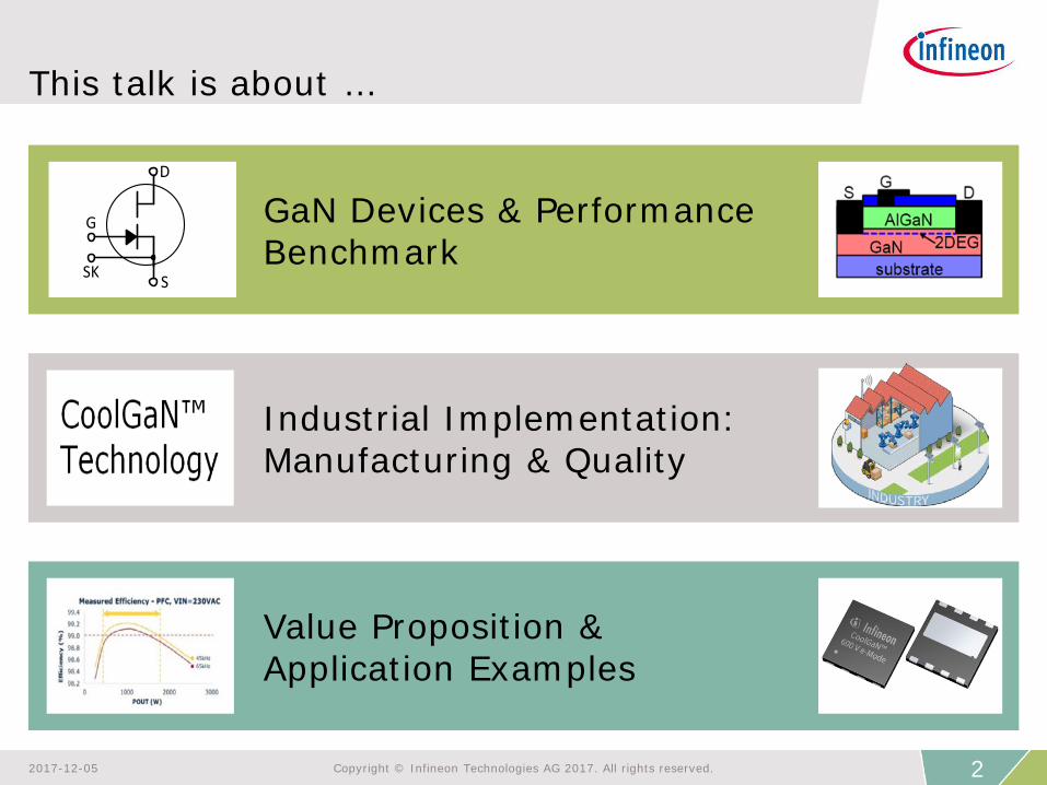
This talk is about …
GaN Devices & Performance Benchmark
G
SK
D
S
Value Proposition & Application Examples
Industrial Implementation: Manufacturing & Quality
22017-12-05 Copyright © Infineon Technologies AG 2017. All rights reserved.
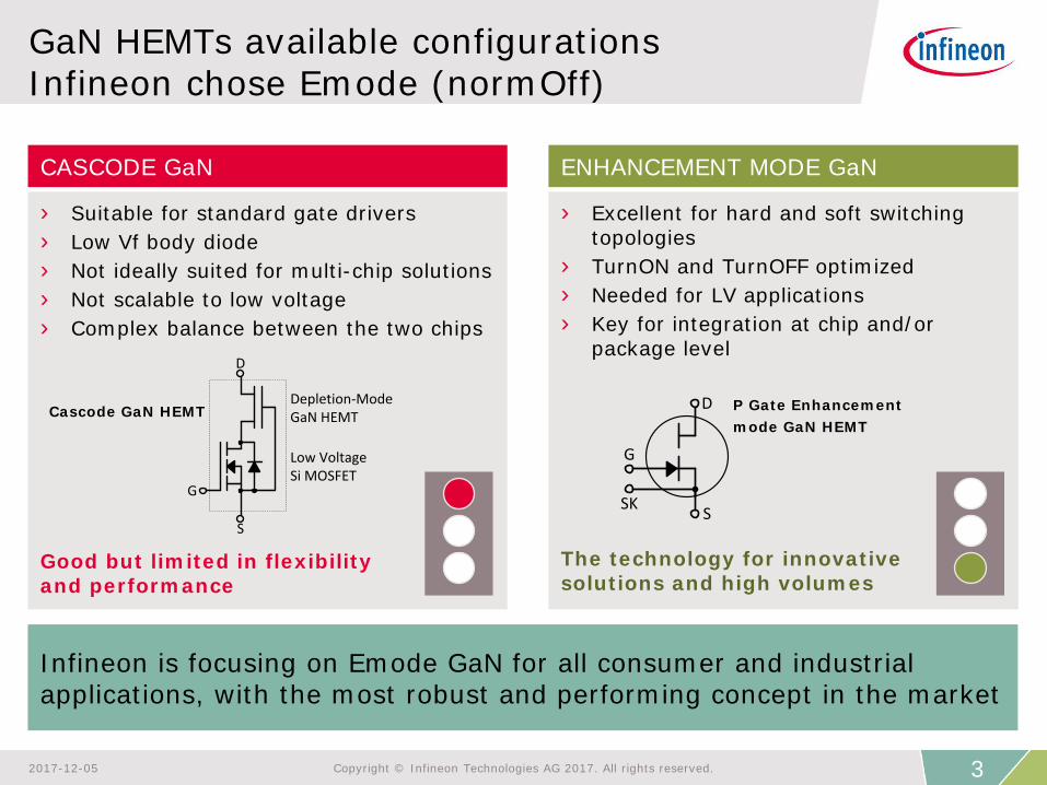
GaN HEMTs available configurationsInfineon chose Emode (normOff)
› Suitable for standard gate drivers› Low Vf body diode› Not ideally suited for multi-chip solutions› Not scalable to low voltage› Complex balance between the two chips
Good but limited in flexibilityand performance
› Excellent for hard and soft switching topologies
› TurnON and TurnOFF optimized› Needed for LV applications› Key for integration at chip and/or
package level
The technology for innovative solutions and high volumes
P Gate Enhancement mode GaN HEMT
D
S
G
Low Voltage Si MOSFET
Depletion-Mode GaN HEMTCascode GaN HEMT
Infineon is focusing on Emode GaN for all consumer and industrial applications, with the most robust and performing concept in the market
ENHANCEMENT MODE GaNCASCODE GaN
G
SK
D
S
32017-12-05 Copyright © Infineon Technologies AG 2017. All rights reserved.
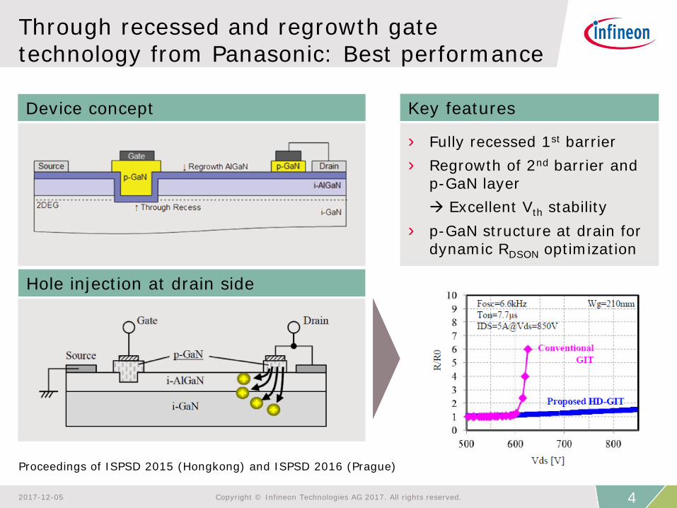
Through recessed and regrowth gate technology from Panasonic: Best performance
› Fully recessed 1st barrier› Regrowth of 2nd barrier and
p-GaN layer Excellent Vth stability
› p-GaN structure at drain for dynamic RDSON optimization
Device concept
Hole injection at drain side
Key features
Proceedings of ISPSD 2015 (Hongkong) and ISPSD 2016 (Prague)
42017-12-05 Copyright © Infineon Technologies AG 2017. All rights reserved.
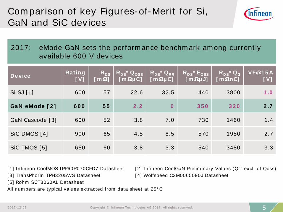
Comparison of key Figures-of-Merit for Si, GaN and SiC devices
Device Rating[V]
RDS[mΩ]
RDS*QOSS[mΩµC]
RDS*QRR[mΩµC]
RDS*EOSS[mΩµJ]
RDS*QG[mΩnC]
VF@15A[V]
Si SJ [1] 600 57 22.6 32.5 440 3800 1.0
GaN eMode [2] 600 55 2.2 0 350 320 2.7
GaN Cascode [3] 600 52 3.8 7.0 730 1460 1.4
SiC DMOS [4] 900 65 4.5 8.5 570 1950 2.7
SiC TMOS [5] 650 60 3.8 3.3 540 3480 3.3
[1] Infineon CoolMOS IPP60R070CFD7 Datasheet [2] Infineon CoolGaN Preliminary Values (Qrr excl. of Qoss)[3] TransPhorm TPH3205WS Datasheet [4] Wolfspeed C3M0065090J Datasheet[5] Rohm SCT3060AL DatasheetAll numbers are typical values extracted from data sheet at 25°C
52017-12-05 Copyright © Infineon Technologies AG 2017. All rights reserved.
2017: eMode GaN sets the performance benchmark among currently available 600 V devices
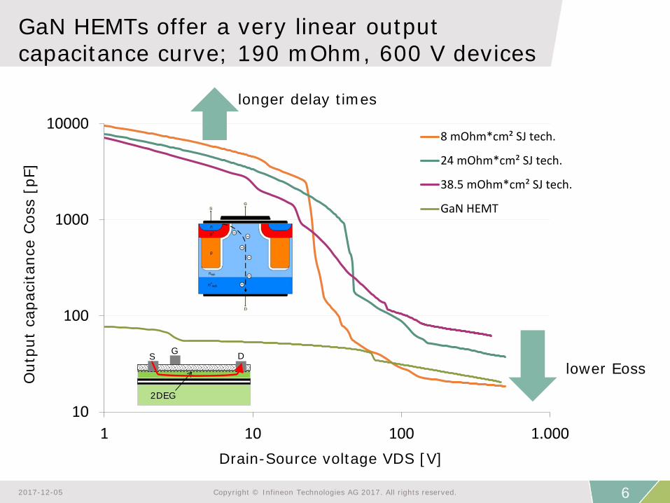
10
100
1000
10000
1 10 100 1.000
Out
put
capa
cita
nce
Cos
s [p
F]
Drain-Source voltage VDS [V]
8 mOhm*cm² SJ tech.
24 mOhm*cm² SJ tech.
38.5 mOhm*cm² SJ tech.
GaN HEMT
GaN HEMTs offer a very linear output capacitance curve; 190 mOhm, 600 V devices
lower Eoss
longer delay times
S G D
2DEG
62017-12-05 Copyright © Infineon Technologies AG 2017. All rights reserved.

Industrial Implementation: Manufacturing
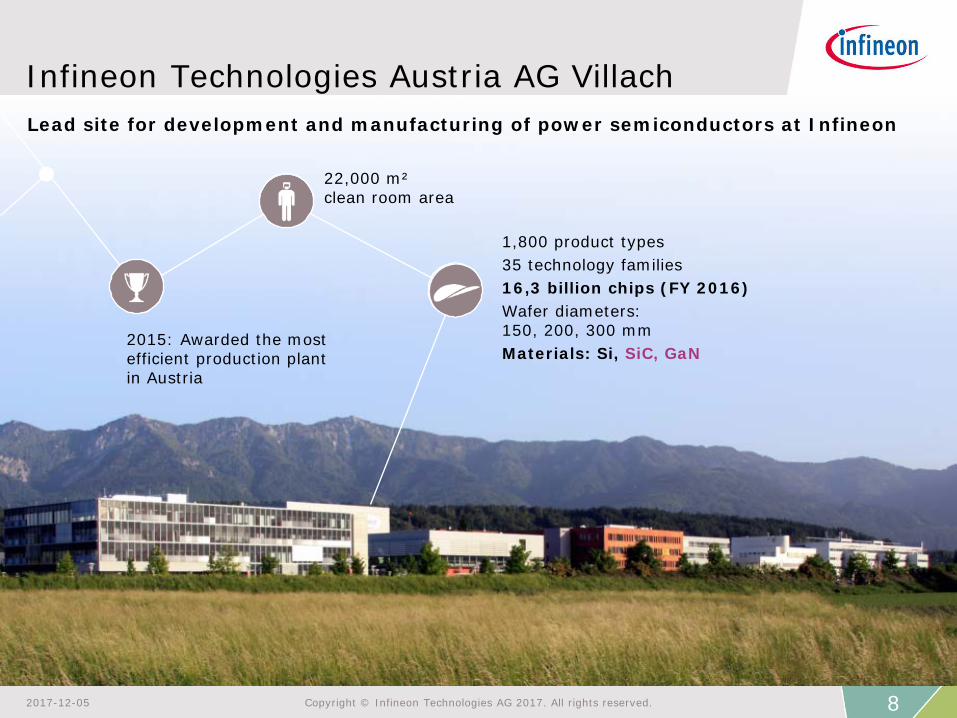
Infineon Technologies Austria AG VillachLead site for development and manufacturing of power semiconductors at Infineon
2015: Awarded the most efficient production plant in Austria
1,800 product types35 technology families16,3 billion chips (FY 2016)Wafer diameters:150, 200, 300 mmMaterials: Si, SiC, GaN
22,000 m²clean room area
82017-12-05 Copyright © Infineon Technologies AG 2017. All rights reserved.
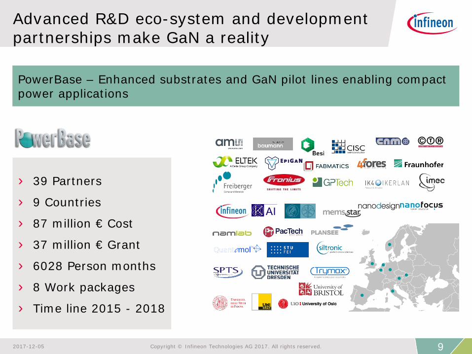
Advanced R&D eco-system and development partnerships make GaN a reality
› 39 Partners
› 9 Countries
› 87 million € Cost
› 37 million € Grant
› 6028 Person months
› 8 Work packages
› Time line 2015 - 2018
92017-12-05 Copyright © Infineon Technologies AG 2017. All rights reserved.
PowerBase – Enhanced substrates and GaN pilot lines enabling compact power applications
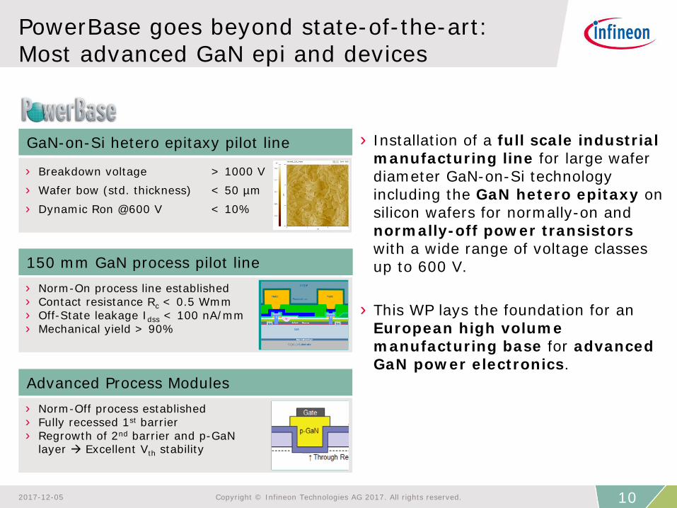
PowerBase goes beyond state-of-the-art:Most advanced GaN epi and devices
150 mm GaN process pilot line › Norm-On process line established› Contact resistance Rc < 0.5 Wmm› Off-State leakage Idss < 100 nA/mm› Mechanical yield > 90%
Advanced Process Modules› Norm-Off process established› Fully recessed 1st barrier› Regrowth of 2nd barrier and p-GaN
layer Excellent Vth stability
› Installation of a full scale industrial manufacturing line for large wafer diameter GaN-on-Si technology including the GaN hetero epitaxy on silicon wafers for normally-on and normally-off power transistors with a wide range of voltage classes up to 600 V.
› This WP lays the foundation for an European high volume manufacturing base for advanced GaN power electronics.
› Breakdown voltage > 1000 V› Wafer bow (std. thickness) < 50 µm› Dynamic Ron @600 V < 10%
GaN-on-Si hetero epitaxy pilot line
102017-12-05 Copyright © Infineon Technologies AG 2017. All rights reserved.

Industrial Implementation:Quality
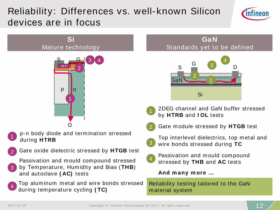
SiMature technology
GaNStandards yet to be defined
Reliability: Differences vs. well-known Silicon devices are in focus
S G
D
p n
p+n+ S
G D
Gate oxide dielectric stressed by HTGB test
p-n body diode and termination stressed during HTRB
Top aluminum metal and wire bonds stressed during temperature cycling (TC)
Passivation and mould compound stressed by Temperature, Humidity and Bias (THB)and autoclave (AC) tests
1
2
3
4
1
23 4
2DEG channel and GaN buffer stressed by HTRB and IOL tests
Top interlevel dielectrics, top metal and wire bonds stressed during TC
Reliability testing tailored to the GaN material system
1
1
2
Passivation and mould compound stressed by THB and AC tests
2
Gate module stressed by HTGB test
3
34
4
Si
GaN
And many more …
122017-12-05 Copyright © Infineon Technologies AG 2017. All rights reserved.
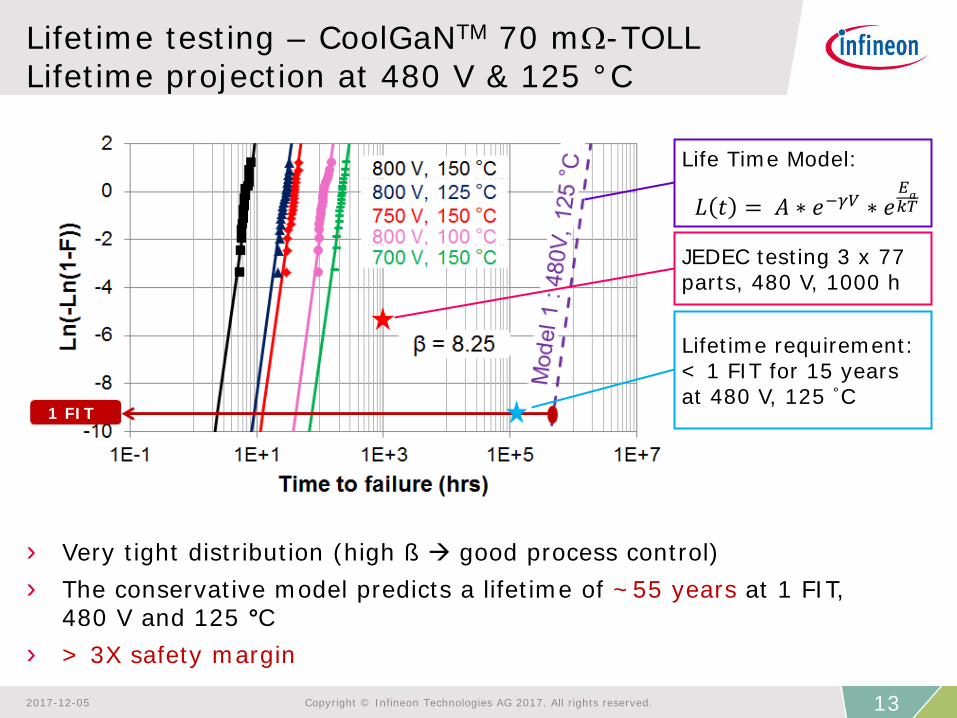
𝐿𝐿 𝑡𝑡 = 𝐴𝐴 ∗ 𝑒𝑒−𝛾𝛾𝛾𝛾 ∗ 𝑒𝑒𝐸𝐸𝑎𝑎𝑘𝑘𝑘𝑘
Life Time Model:
Lifetime requirement:< 1 FIT for 15 years at 480 V, 125 °C
› Very tight distribution (high ß good process control)› The conservative model predicts a lifetime of ~55 years at 1 FIT,
480 V and 125 °C› > 3X safety margin
Lifetime testing – CoolGaNTM 70 mΩ-TOLLLifetime projection at 480 V & 125 °C
JEDEC testing 3 x 77 parts, 480 V, 1000 h
132017-12-05 Copyright © Infineon Technologies AG 2017. All rights reserved.
1 FIT
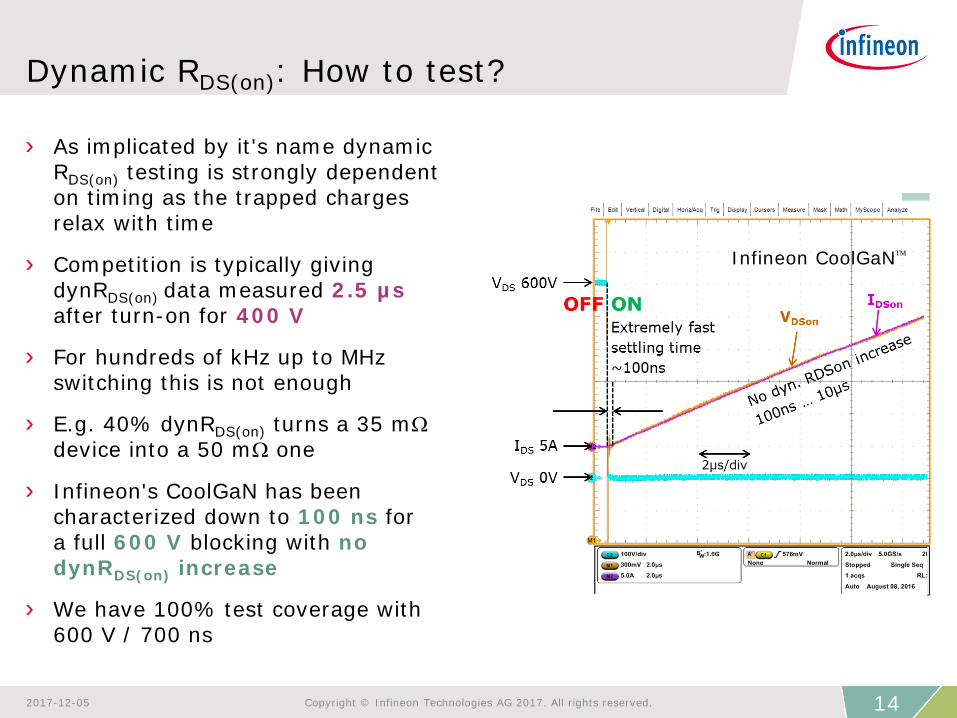
Dynamic RDS(on): How to test?
› As implicated by it's name dynamicRDS(on) testing is strongly dependenton timing as the trapped chargesrelax with time
› Competition is typically givingdynRDS(on) data measured 2.5 µsafter turn-on for 400 V
› For hundreds of kHz up to MHz switching this is not enough
› E.g. 40% dynRDS(on) turns a 35 mΩdevice into a 50 mΩ one
› Infineon's CoolGaN has been characterized down to 100 ns fora full 600 V blocking with no dynRDS(on) increase
› We have 100% test coverage with 600 V / 700 ns
Infineon CoolGaN
142017-12-05 Copyright © Infineon Technologies AG 2017. All rights reserved.
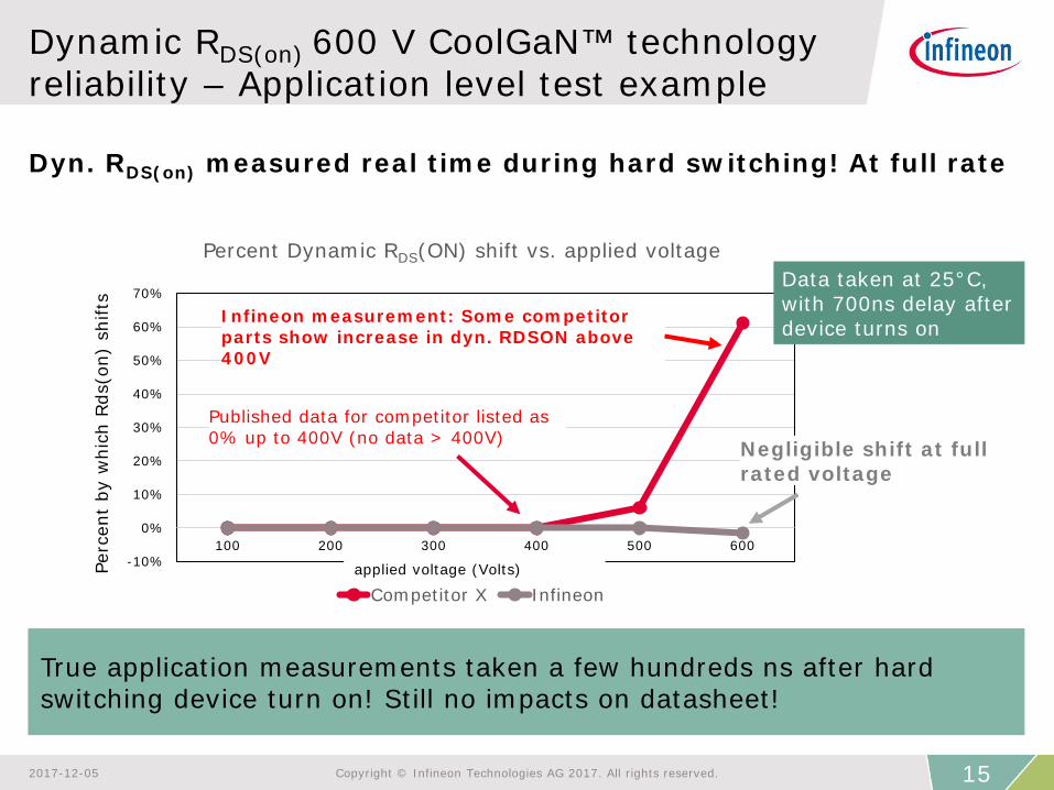
Dynamic RDS(on) 600 V CoolGaN™ technology reliability – Application level test example
Dyn. RDS(on) measured real time during hard switching! At full rate
152017-12-05 Copyright © Infineon Technologies AG 2017. All rights reserved.
True application measurements taken a few hundreds ns after hard switching device turn on! Still no impacts on datasheet!
-10%
0%
10%
20%
30%
40%
50%
60%
70%
100 200 300 400 500 600
Percent Dynamic RDS(ON) shift vs. applied voltage
Competitor X Infineonapplied voltage (Volts)
Infineon measurement: Some competitor parts show increase in dyn. RDSON above 400V
Perc
ent
by w
hich
Rds
(on)
shi
fts
Published data for competitor listed as 0% up to 400V (no data > 400V) Negligible shift at full
rated voltage
Data taken at 25°C, with 700ns delay after device turns on
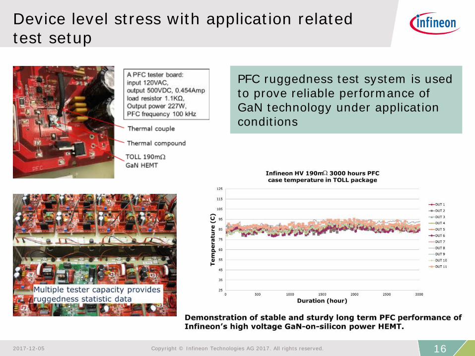
Device level stress with application related test setup
PFC ruggedness test system is used to prove reliable performance of GaN technology under application conditions
Ω
Ω
162017-12-05 Copyright © Infineon Technologies AG 2017. All rights reserved.
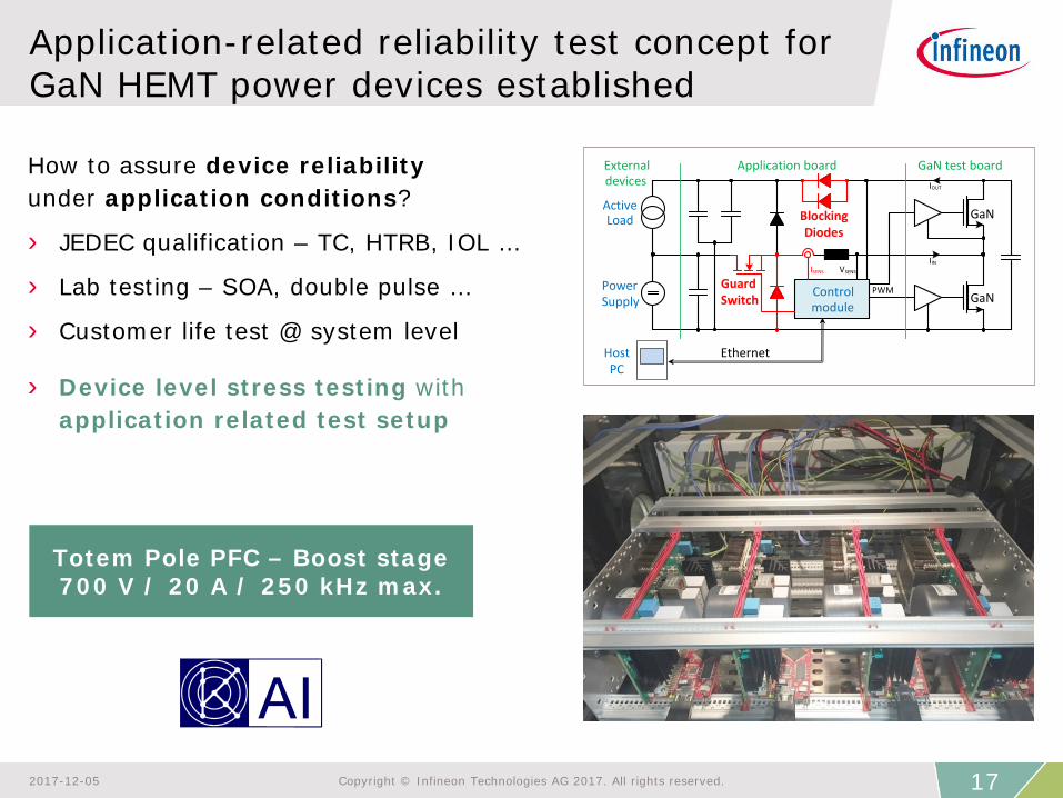
Application-related reliability test concept for GaN HEMT power devices established
How to assure device reliabilityunder application conditions?
› JEDEC qualification – TC, HTRB, IOL …
› Lab testing – SOA, double pulse …
› Customer life test @ system level
› Device level stress testing withapplication related test setup
Control module
PWM Guard Switch
Power Supply
Active Load GaN
GaN
External devices
Application board GaN test board
I IN
I OUT
I SENS V SENS
Blocking Diodes
HostPC
Ethernet
Totem Pole PFC – Boost stage700 V / 20 A / 250 kHz max.
172017-12-05 Copyright © Infineon Technologies AG 2017. All rights reserved.

Value Proposition & Application Examples
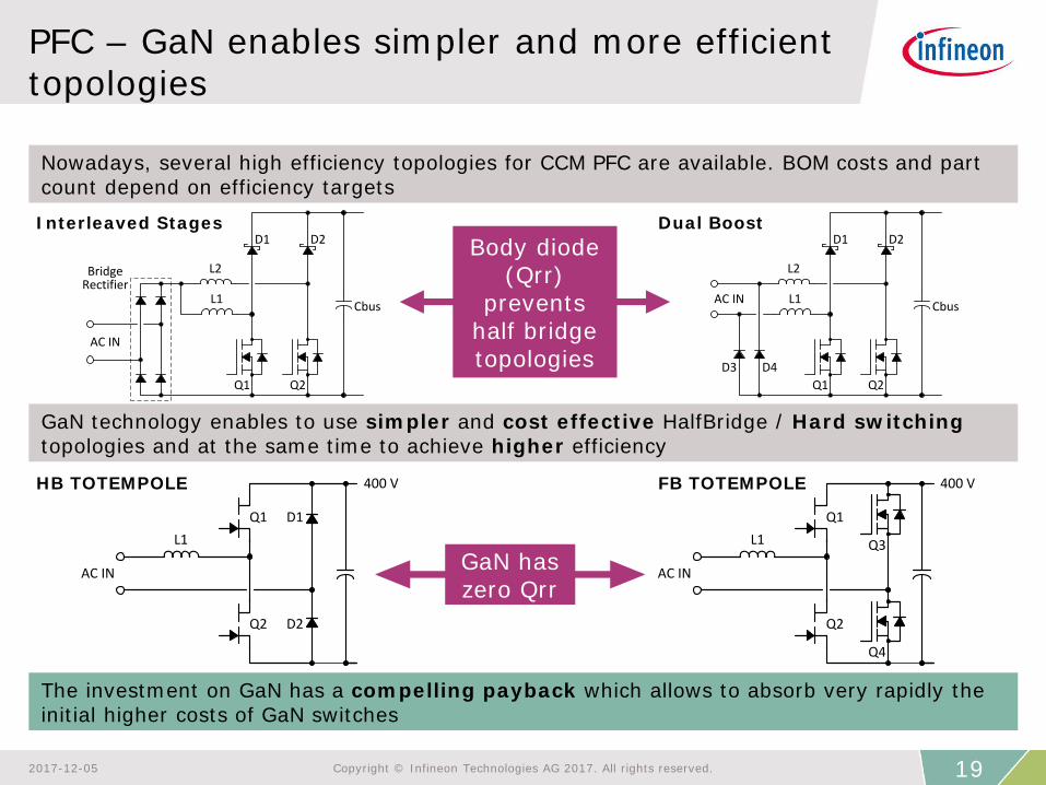
PFC – GaN enables simpler and more efficient topologies
Interleaved Stages Dual Boost
HB TOTEMPOLE FB TOTEMPOLE
Nowadays, several high efficiency topologies for CCM PFC are available. BOM costs and part count depend on efficiency targets
Q3
400 V
AC IN
Q4
L1Q1
Q2
D1
400 V
AC IN
D2
L1Q1
Q2
Q1
D1
L1
AC IN
D2
Q2
L2
Cbus
Bridge Rectifier
Q1
D1
L1AC IN
D2
Q2
L2
Cbus
D3 D4
GaN has zero Qrr
Body diode (Qrr)
prevents half bridge topologies
GaN technology enables to use simpler and cost effective HalfBridge / Hard switchingtopologies and at the same time to achieve higher efficiency
The investment on GaN has a compelling payback which allows to absorb very rapidly the initial higher costs of GaN switches
192017-12-05 Copyright © Infineon Technologies AG 2017. All rights reserved.
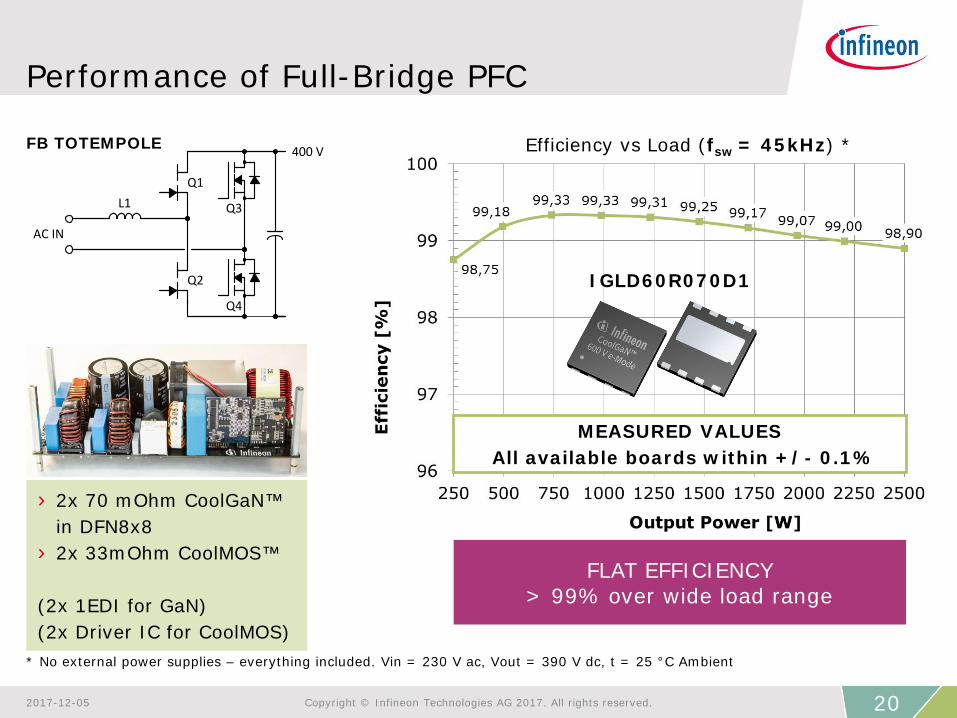
FLAT EFFICIENCY> 99% over wide load range
Performance of Full-Bridge PFC
Q3
400 V
AC IN
Q4
L1Q1
Q2
FB TOTEMPOLE
› 2x 70 mOhm CoolGaN™in DFN8x8
› 2x 33mOhm CoolMOS™
(2x 1EDI for GaN)(2x Driver IC for CoolMOS)
MEASURED VALUESAll available boards within +/- 0.1%
Efficiency vs Load (fsw = 45kHz) *
IGLD60R070D1
* No external power supplies – everything included. Vin = 230 V ac, Vout = 390 V dc, t = 25 °C Ambient
202017-12-05 Copyright © Infineon Technologies AG 2017. All rights reserved.

Typical application example: High-Power SMPS
212017-12-05 Copyright © Infineon Technologies AG 2017. All rights reserved.
Totem-Pole Full-Bridge PFC Stage LLC Resonant DC-DC with Sync Rectifier
CoolGaN™ Half-bridge + CoolMOS™ Half-bridge
OptiMOS™ Sync-Rect(LV GaN in development)CoolGaN™ Full-bridge
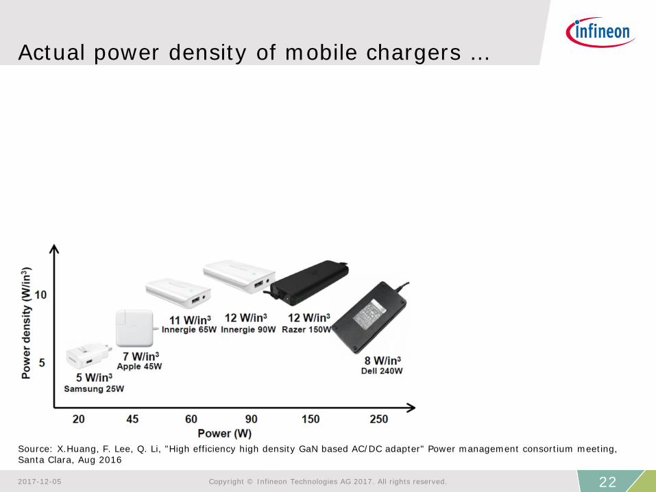
Actual power density of mobile chargers …
Source: X.Huang, F. Lee, Q. Li, "High efficiency high density GaN based AC/DC adapter" Power management consortium meeting, Santa Clara, Aug 2016
222017-12-05 Copyright © Infineon Technologies AG 2017. All rights reserved.
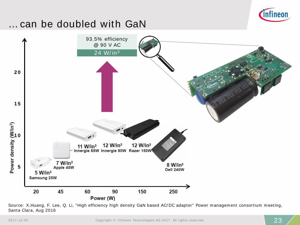
… can be doubled with GaN
24 W/in3
93.5% efficiency@ 90 V AC
10
5
20
15
232017-12-05 Copyright © Infineon Technologies AG 2017. All rights reserved.
Source: X.Huang, F. Lee, Q. Li, "High efficiency high density GaN based AC/DC adapter" Power management consortium meeting, Santa Clara, Aug 2016
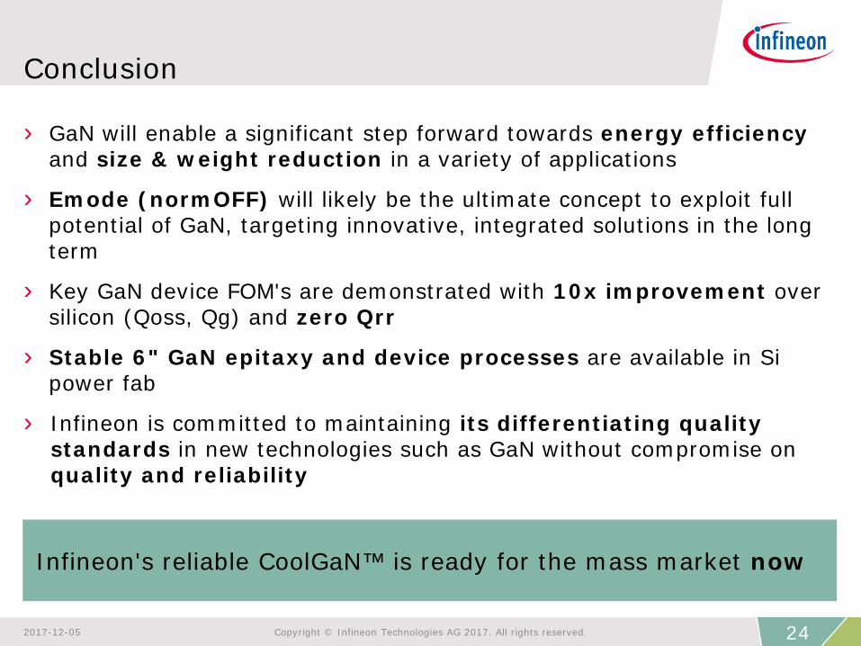
Conclusion
Infineon's reliable CoolGaN™ is ready for the mass market now
› GaN will enable a significant step forward towards energy efficiencyand size & weight reduction in a variety of applications
› Emode (normOFF) will likely be the ultimate concept to exploit full potential of GaN, targeting innovative, integrated solutions in the long term
› Key GaN device FOM's are demonstrated with 10x improvement over silicon (Qoss, Qg) and zero Qrr
› Stable 6" GaN epitaxy and device processes are available in Si power fab
› Infineon is committed to maintaining its differentiating quality standards in new technologies such as GaN without compromise on quality and reliability
242017-12-05 Copyright © Infineon Technologies AG 2017. All rights reserved.

Acknowledgement
252017-12-05 Copyright © Infineon Technologies AG 2017. All rights reserved.
The project "PowerBase" has received funding from the Electronic Component Systems for European Leadership Joint Undertaking under grant agreement No 662133.
This Joint Undertaking receives support from the European Union's Horizon 2020 research and innovation program and from Austria, Belgium, Germany, Italy, Netherlands, Norway, Slovakia, Spain and the United Kingdom.
A big Thank You to all colleagues and partners involved in Infineon's GaN program!

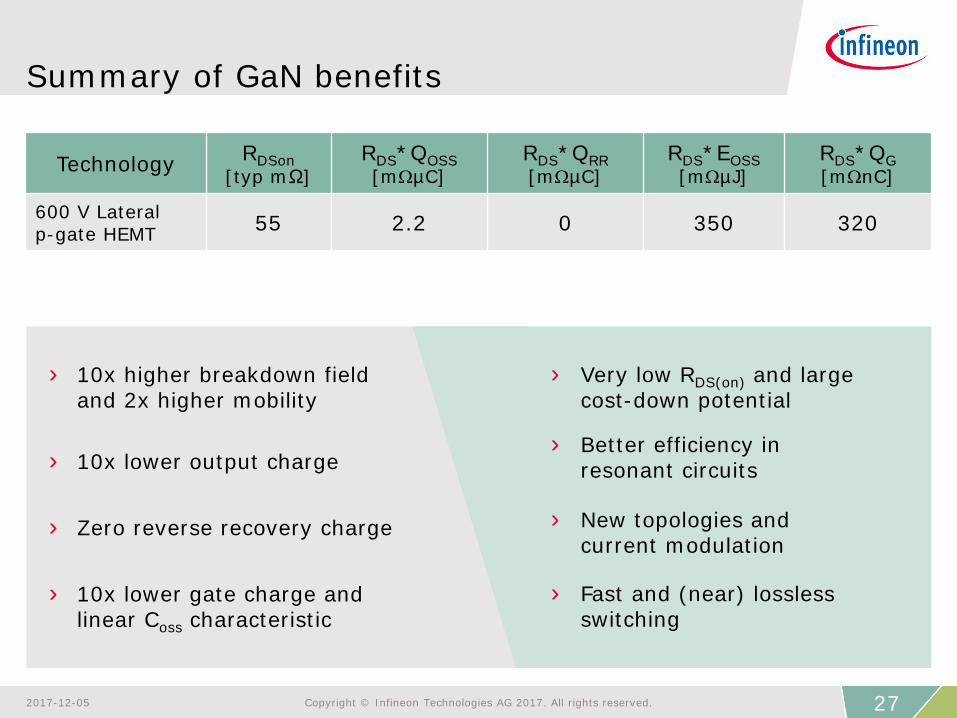
Technology RDSon[typ mΩ]
RDS*QOSS[mΩµC]
RDS*QRR[mΩµC]
RDS*EOSS[mΩµJ]
RDS*QG[mΩnC]
600 V Lateralp-gate HEMT 55 2.2 0 350 320
Summary of GaN benefits
› Fast and (near) losslessswitching
› 10x higher breakdown fieldand 2x higher mobility
› Very low RDS(on) and largecost-down potential
› 10x lower output charge
› Zero reverse recovery charge
› 10x lower gate charge andlinear Coss characteristic
› Better efficiency inresonant circuits
› New topologies andcurrent modulation
272017-12-05 Copyright © Infineon Technologies AG 2017. All rights reserved.