Embed Size (px)
Citation preview
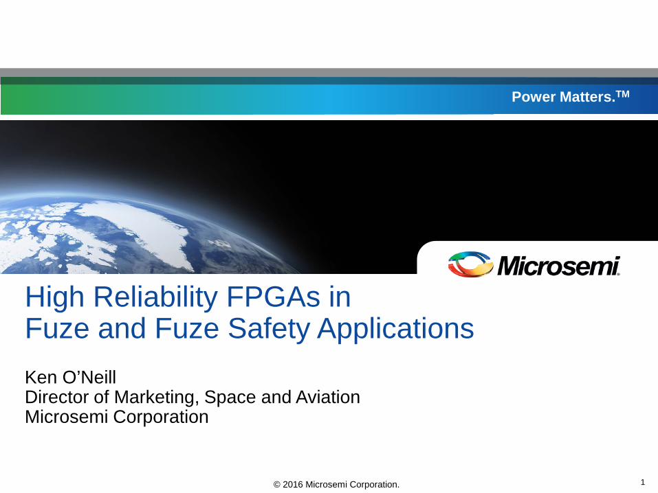
© 2016 Microsemi Corporation. 1
Power Matters.TM
High Reliability FPGAs in Fuze and Fuze Safety Applications Ken O’Neill Director of Marketing, Space and Aviation Microsemi Corporation
Power Matters.TM 2 © 2016 Microsemi Corporation.
Why use FPGAs in Fuze applications
Antifuse FPGAs in Fuze and Fuze safety systems • Heritage and Outlook
Flash FPGAs – considerations for Fuze Safety and Arming
• Architecture and Programming • Reliability, Retention, Qualification • Radiation • Power consumption • Heritage and Outlook
Conclusion
Agenda
Power Matters.TM 3 © 2016 Microsemi Corporation.
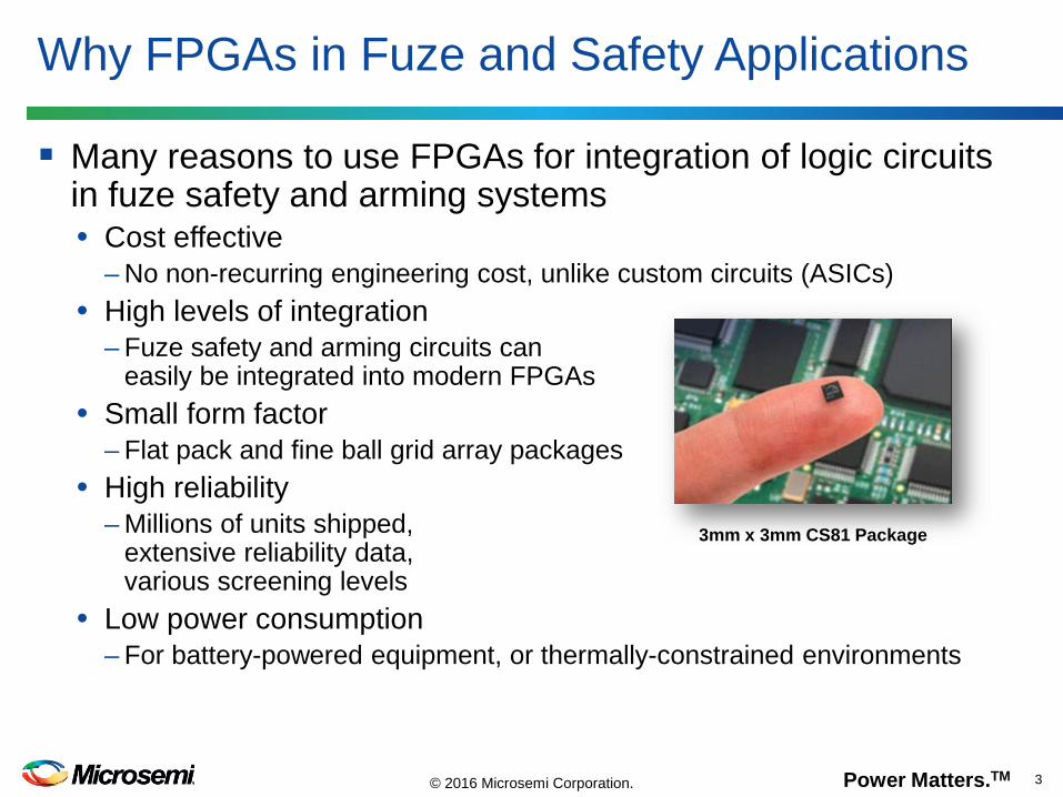
Many reasons to use FPGAs for integration of logic circuits in fuze safety and arming systems • Cost effective
– No non-recurring engineering cost, unlike custom circuits (ASICs) • High levels of integration
– Fuze safety and arming circuits can easily be integrated into modern FPGAs
• Small form factor – Flat pack and fine ball grid array packages
• High reliability – Millions of units shipped,
extensive reliability data, various screening levels
• Low power consumption – For battery-powered equipment, or thermally-constrained environments
Why FPGAs in Fuze and Safety Applications
3mm x 3mm CS81 Package

Power Matters.TM 4 © 2016 Microsemi Corporation.
Microsemi antifuse FPGAs have a long heritage in fuze applications
Antifuse FPGAs in Fuze applications

Power Matters.TM 5 © 2016 Microsemi Corporation.
Microsemi has a policy of long term production • We hold many years of wafer stock after fab production has ended • 12 month last time buy, plus 6 month shipment window after final order
No new antifuse technology introduction since 150nm in 2002
Now is the time to start thinking about Flash FPGA technology
for next generation fuze safety and arming systems
Antifuse FPGA Outlook
2015 2010 2005 2000 1995
AX Family 150nm, 10K Logic Elements
SX / SX-A Family 220nm, 2K Logic Elements
MX Family 450nm, 1K Logic Elements
RTAX Family 150nm, 20KLE (Space Grade)

Power Matters.TM 6 © 2016 Microsemi Corporation.
Flash FPGAs Considerations for Fuze Safety and Arming
Power Matters.TM 7 © 2016 Microsemi Corporation.
Introduction to Flash FPGAs
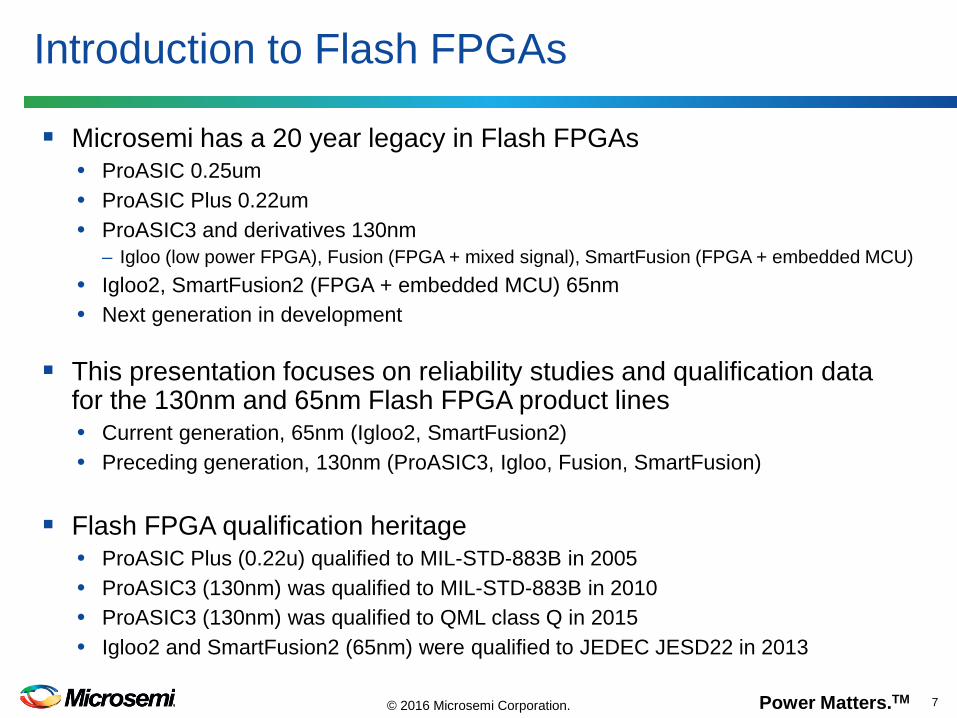
Microsemi has a 20 year legacy in Flash FPGAs • ProASIC 0.25um • ProASIC Plus 0.22um • ProASIC3 and derivatives 130nm
– Igloo (low power FPGA), Fusion (FPGA + mixed signal), SmartFusion (FPGA + embedded MCU) • Igloo2, SmartFusion2 (FPGA + embedded MCU) 65nm • Next generation in development
This presentation focuses on reliability studies and qualification data for the 130nm and 65nm Flash FPGA product lines • Current generation, 65nm (Igloo2, SmartFusion2) • Preceding generation, 130nm (ProASIC3, Igloo, Fusion, SmartFusion)
Flash FPGA qualification heritage • ProASIC Plus (0.22u) qualified to MIL-STD-883B in 2005 • ProASIC3 (130nm) was qualified to MIL-STD-883B in 2010 • ProASIC3 (130nm) was qualified to QML class Q in 2015 • Igloo2 and SmartFusion2 (65nm) were qualified to JEDEC JESD22 in 2013
Power Matters.TM 8 © 2016 Microsemi Corporation.
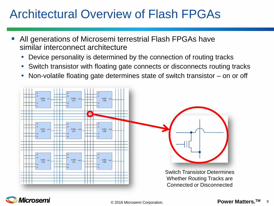
All generations of Microsemi terrestrial Flash FPGAs have similar interconnect architecture • Device personality is determined by the connection of routing tracks • Switch transistor with floating gate connects or disconnects routing tracks • Non-volatile floating gate determines state of switch transistor – on or off
Architectural Overview of Flash FPGAs
Switch Transistor Determines Whether Routing Tracks are Connected or Disconnected

Power Matters.TM 9 © 2016 Microsemi Corporation.
Flash Cell Architecture
In Microsemi Flash-based FPGAs, each switch transistor is accompanied by a sense transistor which shares the same floating gate and control gate
The sense transistor is used for programming, erasing, and margining
Power Matters.TM 10 © 2016 Microsemi Corporation.
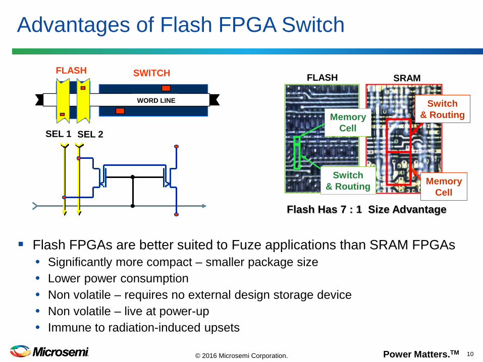
Flash FPGAs are better suited to Fuze applications than SRAM FPGAs • Significantly more compact – smaller package size • Lower power consumption • Non volatile – requires no external design storage device • Non volatile – live at power-up • Immune to radiation-induced upsets
Advantages of Flash FPGA Switch
SEL 1 SEL 2
SWITCH FLASH
WORD LINE
SRAM FLASH
Flash Has 7 : 1 Size Advantage
Switch & Routing
Memory Cell
Switch & Routing
Memory Cell

Power Matters.TM 11 © 2016 Microsemi Corporation.
ProASIC3 Logic Cell implements any 3-input combinatorial logic function or a D-type Flip Flop with enable
ProASIC3 Basic Logic Cell (130nm)
0
1 0
1
YL (long)
I2 (X1) Pin 2 Set/Reset
I5 (X2) Pin 3 CLK
I8 (X3) Pin 4 Data
L10
L9 L8
L4
L5 L6
L7
L11
L2 L0 L13 L3 L1 L15 L12 L14
F2 (local)
Each logic cell is equivalent to
1 to 8 ASIC gates
Power Matters.TM 12 © 2016 Microsemi Corporation.
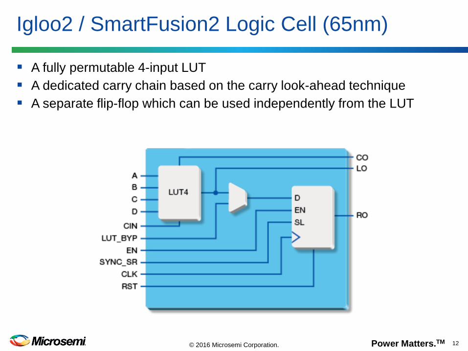
Igloo2 / SmartFusion2 Logic Cell (65nm)
A fully permutable 4-input LUT A dedicated carry chain based on the carry look-ahead technique A separate flip-flop which can be used independently from the LUT
Power Matters.TM 13 © 2016 Microsemi Corporation.
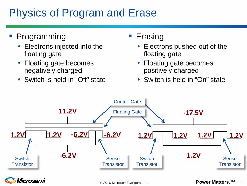
Physics of Program and Erase
Programming • Electrons injected into the
floating gate • Floating gate becomes
negatively charged • Switch is held in “Off” state
Erasing • Electrons pushed out of the
floating gate • Floating gate becomes
positively charged • Switch is held in “On” state
11.2V
1.2V 1.2V -6.2V -6.2V
-6.2V
-17.5V
1.2V 1.2V 1.2V 1.2V
1.2V
Floating Gate
Control Gate
Sense Transistor
Switch Transistor
Sense Transistor
Switch Transistor

Power Matters.TM 14 © 2016 Microsemi Corporation.
What is Margining?
What is margining? • Margining is the operation for determining the amount of charge in
the flash cell Why do we need it?
• In order to do any flash reliability studies, the ability to accurately track the amount of charge in a floating gate is essential
One of the unique features of Microsemi Flash FPGAs is
the ability to margin all flash cells in the FPGA fabric even after the part has been packaged
Power Matters.TM 15 © 2016 Microsemi Corporation.
How Margining Works
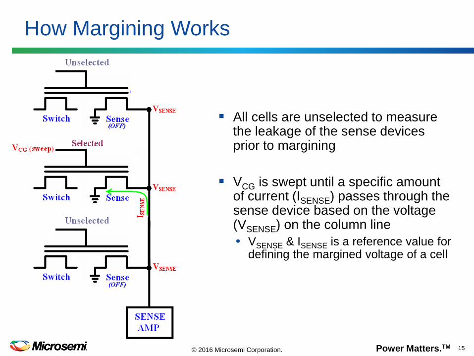
All cells are unselected to measure
the leakage of the sense devices prior to margining
VCG is swept until a specific amount of current (ISENSE) passes through the sense device based on the voltage (VSENSE) on the column line • VSENSE & ISENSE is a reference value for
defining the margined voltage of a cell
Power Matters.TM 16 © 2016 Microsemi Corporation.
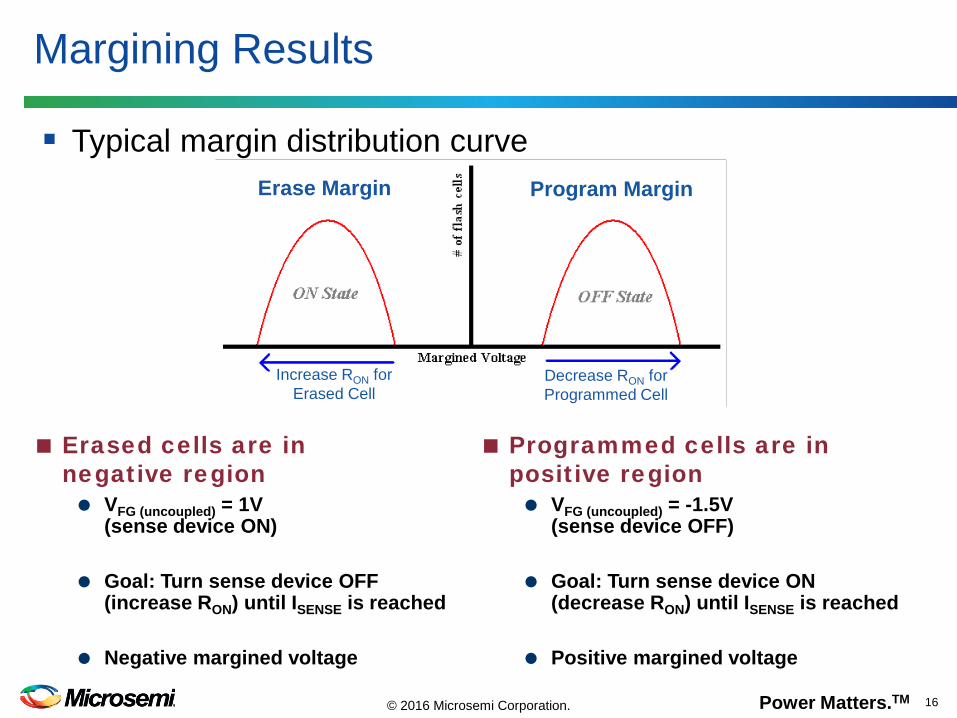
Margining Results
Typical margin distribution curve
Erased cells are in negative region VFG (uncoupled) = 1V
(sense device ON)
Goal: Turn sense device OFF (increase RON) until ISENSE is reached
Negative margined voltage
Programmed cells are in positive region VFG (uncoupled) = -1.5V
(sense device OFF)
Goal: Turn sense device ON (decrease RON) until ISENSE is reached
Positive margined voltage
Erase Margin Program Margin
Decrease RON for Programmed Cell
Increase RON for Erased Cell
Power Matters.TM 17 © 2016 Microsemi Corporation.
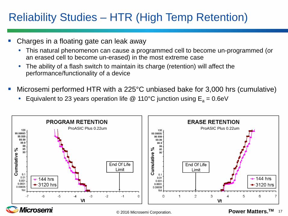
Reliability Studies – HTR (High Temp Retention)
Charges in a floating gate can leak away • This natural phenomenon can cause a programmed cell to become un-programmed (or
an erased cell to become un-erased) in the most extreme case • The ability of a flash switch to maintain its charge (retention) will affect the
performance/functionality of a device
Microsemi performed HTR with a 225°C unbiased bake for 3,000 hrs (cumulative) • Equivalent to 23 years operation life @ 110°C junction using Ea = 0.6eV
ProASIC Plus 0.22um ProASIC Plus 0.22um
Power Matters.TM 18 © 2016 Microsemi Corporation.
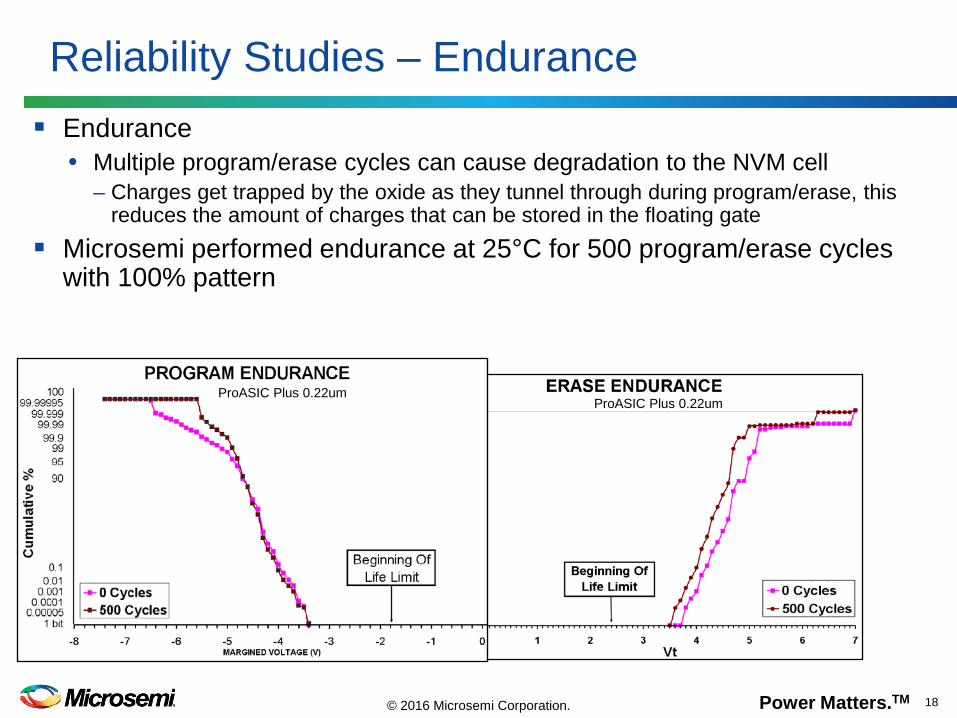
Reliability Studies – Endurance Endurance
• Multiple program/erase cycles can cause degradation to the NVM cell – Charges get trapped by the oxide as they tunnel through during program/erase, this
reduces the amount of charges that can be stored in the floating gate
Microsemi performed endurance at 25°C for 500 program/erase cycles with 100% pattern
ProASIC Plus 0.22um ProASIC Plus 0.22um
Power Matters.TM 19 © 2016 Microsemi Corporation.
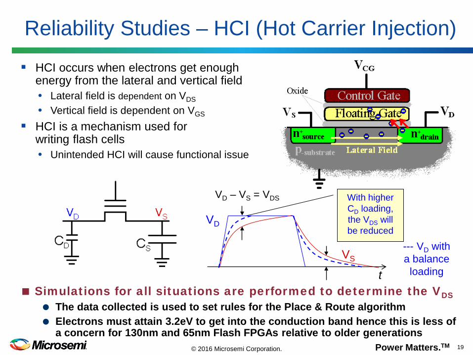
Reliability Studies – HCI (Hot Carrier Injection)
HCI occurs when electrons get enough energy from the lateral and vertical field • Lateral field is dependent on VDS
• Vertical field is dependent on VGS
HCI is a mechanism used for writing flash cells • Unintended HCI will cause functional issue
t
VD – VS = VDS
VD
VS
With higher CD loading, the VDS will be reduced
--- VD with a balance loading
Simulations for all situations are performed to determine the VDS The data collected is used to set rules for the Place & Route algorithm Electrons must attain 3.2eV to get into the conduction band hence this is less of
a concern for 130nm and 65nm Flash FPGAs relative to older generations
Power Matters.TM 20 © 2016 Microsemi Corporation.
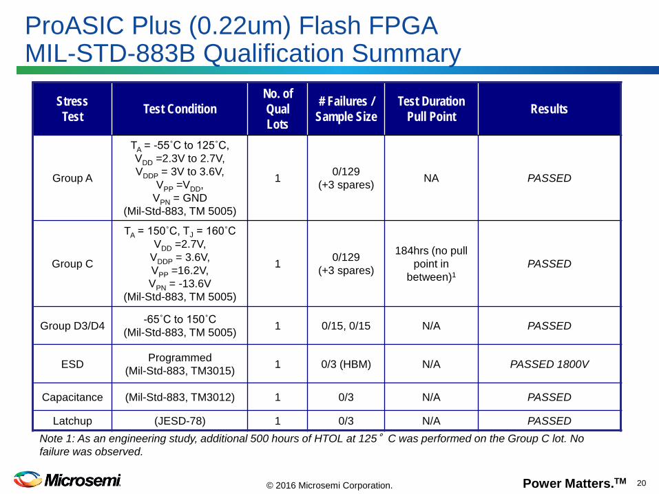
ProASIC Plus (0.22um) Flash FPGA MIL-STD-883B Qualification Summary
Stress Test Test Condition
No. of Qual Lots
# Failures / Sample Size
Test Duration Pull Point Results
Group A
TA = -55˚C to 125˚C, VDD =2.3V to 2.7V, VDDP = 3V to 3.6V,
VPP =VDD, VPN = GND
(Mil-Std-883, TM 5005)
1 0/129 (+3 spares) NA PASSED
Group C
TA = 150˚C, TJ = 160˚C VDD =2.7V,
VDDP = 3.6V, VPP =16.2V, VPN = -13.6V
(Mil-Std-883, TM 5005)
1 0/129 (+3 spares)
184hrs (no pull point in
between)1 PASSED
Group D3/D4 -65˚C to 150˚C (Mil-Std-883, TM 5005) 1 0/15, 0/15 N/A PASSED
ESD Programmed (Mil-Std-883, TM3015) 1 0/3 (HBM) N/A PASSED 1800V
Capacitance (Mil-Std-883, TM3012) 1 0/3 N/A PASSED
Latchup (JESD-78) 1 0/3 N/A PASSED Note 1: As an engineering study, additional 500 hours of HTOL at 125°C was performed on the Group C lot. No failure was observed.

Power Matters.TM 21 © 2016 Microsemi Corporation.
ProASIC3 (130nm) Flash FPGA MIL-STD-883B Qualification Summary
Power Matters.TM 22 © 2016 Microsemi Corporation.
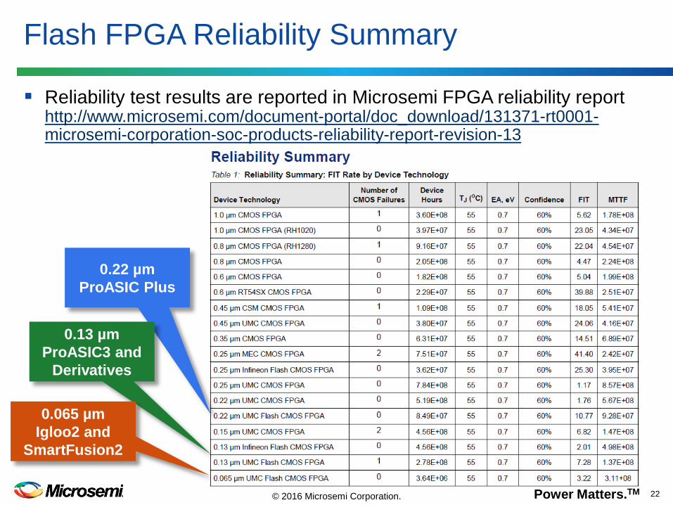
Reliability test results are reported in Microsemi FPGA reliability report http://www.microsemi.com/document-portal/doc_download/131371-rt0001-microsemi-corporation-soc-products-reliability-report-revision-13
Flash FPGA Reliability Summary
0.22 µm ProASIC Plus
0.13 µm ProASIC3 and
Derivatives
0.065 µm Igloo2 and
SmartFusion2
Power Matters.TM 23 © 2016 Microsemi Corporation.
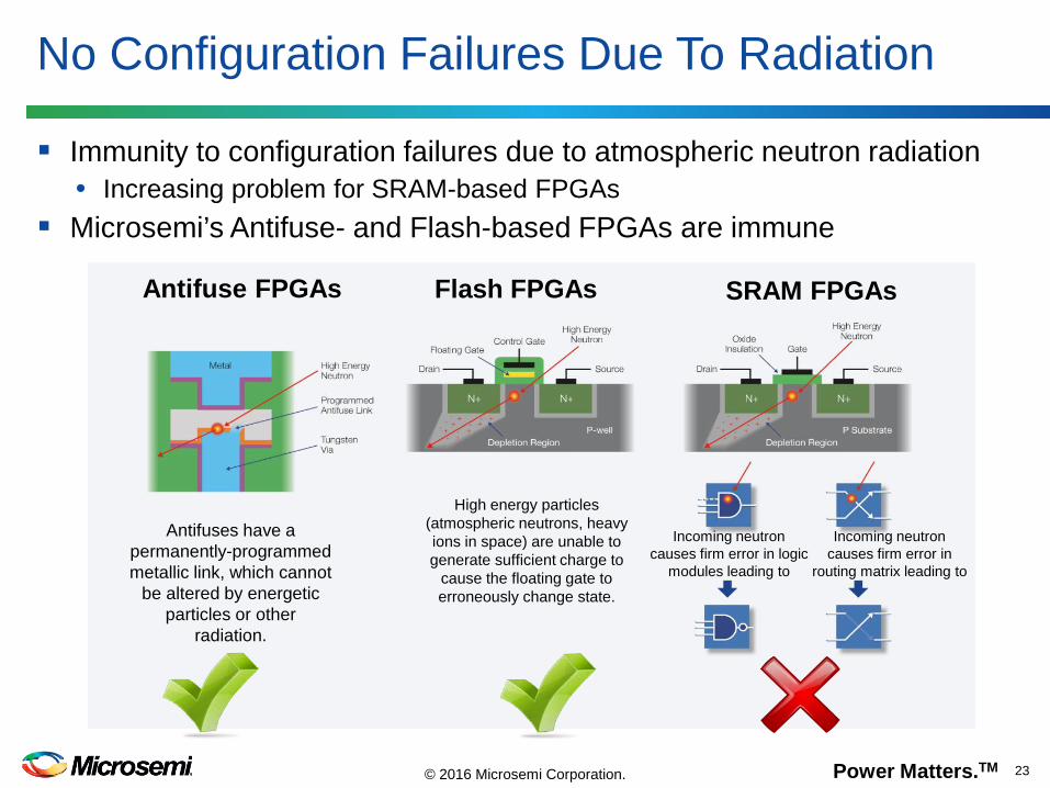
No Configuration Failures Due To Radiation
Antifuse FPGAs Flash FPGAs SRAM FPGAs
Antifuses have a permanently-programmed metallic link, which cannot
be altered by energetic particles or other
radiation.
High energy particles (atmospheric neutrons, heavy ions in space) are unable to generate sufficient charge to
cause the floating gate to erroneously change state.
Incoming neutron causes firm error in logic
modules leading to
Incoming neutron causes firm error in
routing matrix leading to
Immunity to configuration failures due to atmospheric neutron radiation • Increasing problem for SRAM-based FPGAs
Microsemi’s Antifuse- and Flash-based FPGAs are immune

Power Matters.TM 24 © 2016 Microsemi Corporation.
Contact Microsemi for further information [email protected]
Weapon Effect Radiation Testing
Microsemi FPGAs for Strategic ApplicationsProASIC3
IglooIgloo2
SmartFusion2Dose Rate (Upset, rad/sec) 1.4E+10 2.7E+09Dose Rate (Survive, rad/sec) >7.8E+10 >6.1E+10Technology 130nm 65nmMil Temp Plastic Yes YesMil Temp Hermetic - -Max LE / FF 75K Tiles 146KMax SRAM 500Kbits 4.5MbitsMax Mathblocks - 240

Power Matters.TM 25 © 2016 Microsemi Corporation.
IGLOO nano offers industry’s lowest power IGLOO family offers Flash*Freeze mode to obtain low static currents Flash*Freeze mode
• Enter and exit ultra-low power mode using single pin control • Retains SRAM content and register data
Industry’s Lowest Power Consumption
IGLOO nano ProASIC3 nano IGLOO IGLOOE IGLOO Plus ProASIC3 ProASIC3E ProASIC3L
Flash*Freeze Mode Yes No Yes Yes Yes No No Yes
Typical Quiescent Current 1.9uA 600uA 4uA 34uA 4uA 2mA 5mA 0.33mA
Static Power 2uW 0.9mW 5uW 40.8uW 5uW 3mW 7.5mW 0.4mW

Power Matters.TM 26 © 2016 Microsemi Corporation.
Used in many safety-critical and mission-critical applications
Flash FPGA Heritage
F-35 JSF
Boeing 787 Airbus A400M
Airbus A350 IRIS
ExoMars TGO LADEE
Orbcomm G2
Space Aviation
Power Matters.TM 27 © 2016 Microsemi Corporation.
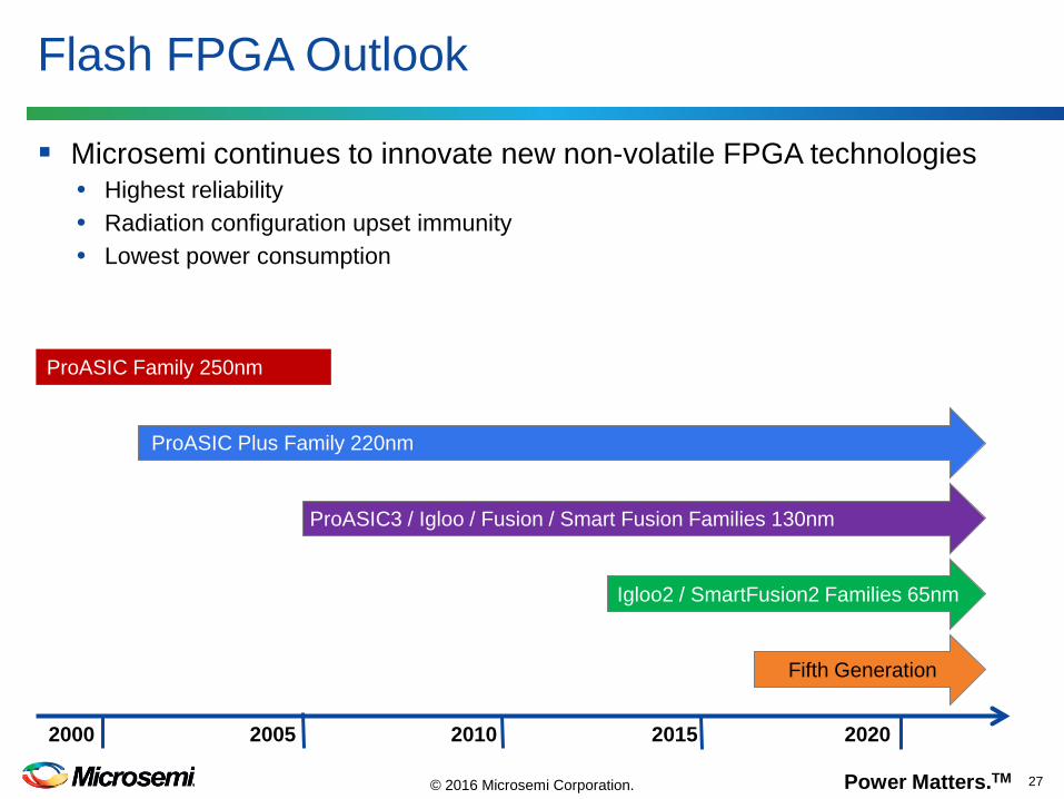
Microsemi continues to innovate new non-volatile FPGA technologies • Highest reliability • Radiation configuration upset immunity • Lowest power consumption
Flash FPGA Outlook
2015 2010 2005 2000
ProASIC3 / Igloo / Fusion / Smart Fusion Families 130nm
ProASIC Plus Family 220nm
ProASIC Family 250nm
Igloo2 / SmartFusion2 Families 65nm
2020
Fifth Generation

Power Matters.TM 28 © 2016 Microsemi Corporation.
CMOS FIT Rate based on HTOL data (cumulative) < 10 FIT for three most recent generations of Microsemi Flash FPGAs • The calculated FIT is based on 60% confidence level @ 55°C using Ea = 0.7eV
Several device-package combinations are available with hermetically sealed ceramic packages and QML class Q or MIL-STD-883 class B screening
Many more device-package combinations are available with plastic packaging and military temperature screening
Reliability Studies performed to date did not reveal any potential issues with four generations of Flash FPGA
Microsemi will continue its commitment to the Defense and Aerospace industries by delivering FPGAs with proven reliability and advanced features
Conclusion
Power Matters.TM 29 © 2016 Microsemi Corporation.
Contact Information
Ken O’Neill
Director of Marketing, Microsemi Corporation
408-643-6179 [email protected]