Embed Size (px)
Citation preview

High-quality Bi2Te3 thin films grown on mica substrates for potentialoptoelectronic applications
K. Wang,1,2 Yanwen Liu,1 Weiyi Wang,1 N. Meyer,2 L. H. Bao,1,2 L. He,3 M. R. Lang,3
Z. G. Chen,4 X. Y. Che,2 K. Post,5 J. Zou,4,6 D. N. Basov,5 K. L. Wang,3 and Faxian Xiu1,a)
1State Key Laboratory of Surface Physics and Department of Physics, Fudan University,Shanghai 200433, China2Department of Electrical and Computer Engineering, Iowa State University, Ames, Iowa 50011, USA3Device Research Laboratory, Department of Electrical Engineering, University of California, Los Angeles,California 90095, USA4Materials Engineering, The University of Queensland, Brisbane QLD 4072, Australia5Department of Physics, University of California, San Diego, California 92093, USA6Center for Microscopy and Microanalysis, The University of Queensland, Brisbane QLD 4072, Australia
(Received 15 April 2013; accepted 26 June 2013; published online 17 July 2013)
We report high-quality topological insulator Bi2Te3 thin films grown on muscovite mica substrates
by molecular beam epitaxy. The topographic and structural analysis revealed that the Bi2Te3 thin
films exhibited atomically smooth terraces over a large area and a high crystalline quality. Both
weak antilocalization effect and quantum oscillations were observed in the magnetotransport of the
relatively thin samples. A phase coherence length of 277 nm for a 6 nm thin film and a high surface
mobility of 0.58 m2 V�1 s�1 for a 4 nm thin film were achieved. These results confirm that the thin
films grown on mica are of high quality. VC 2013 AIP Publishing LLC.
[http://dx.doi.org/10.1063/1.4813903]
Three-dimensional topological insulators (3DTIs)
exhibit a feature of gapless surface states inside the bulk
bandgap, promising potential applications in spintronics,
quantum computation, and thermoelectrics.1 To probe the
exotic phenomena arising from the topologically protected
surface states in 3DTI, the exploitation of high quality mate-
rials is of crucial importance. In practice, because of the
crystal imperfections generated during growth, the carrier
density of bulk outnumbers the surface state, thus, masking
the signature of the surface transport.2 For achieving large-
area TI thin films and heterostructures, molecular beam
epitaxy (MBE) has demonstrated advantages in precisely
controlling the growth rate and obtaining low-defect-density
epilayers. However, owing to the lattice mismatch between
substrates and thin films, amorphous layers often develop
along the interfaces. Additionally, due to the spirals growth
behavior, the steps and voids are produced among the terra-
ces on the surfaces of the thin films, giving rise to a small
effective surface conductance.3–6
One promising approach to improve the crystalline qual-
ity is to grow thin films on weakly interacting substrates via
van der Waals epitaxy (vdWE), which facilitates the growth
of a defect-free epilayer with its own lattice parameters even
from the first layer.7 Muscovite mica with a stoichiometry of
KAl3Si3O10(OH)2 is a well-known substrate that favors the
vdWE growth of semiconductors, metal thin films, and well-
oriented nanowire arrays.8 Its perfect electrical and thermal
insulation, high transparency in ultrathin thickness, and flexi-
bility make it an ideal substrate for TI thin film growth and
the investigation of the corresponding electrical and optical
properties. As a typical 3DTI material, Bi2Te3 has a
rhombohedral crystal structure consisting of quintuple layers
(QLs) stacked along [111] direction.9 Here, we performed
the growth of high-quality Bi2Te3 thin films on mica sub-
strates by MBE. The achieved Bi2Te3 thin films exhibit
ultra-smooth surfaces with large-area terraces as revealed by
atomic force microscopy (AFM). Both the weak antilocaliza-
tion (WAL) effect and quantum oscillations were observed
in the ultrathin thin films by the magnetotransport transport
measurements. The high quality of the thin films on mica
substrates was confirmed by the relatively long phase coher-
ence length and the high surface mobility of electrons.
Bi2Te3 thin films were grown on freshly cleaved mica
in a Perkin-Elmer 430 MBE system with a base pressure of
�3� 10�10 Torr. Reflection high energy electron diffrac-
tion (RHEED) was used to monitor the quality of the thin
film during growth. The topography of thin films was
examined by AFM in a tapping mode, and the thickness
was reliably determined by scanning a scratch deliberately
made on as-grown thin films. The growth rate of the
Bi2Te3 was maintained at �0.5 QL/min. Further structural
analyses were carried out on a Siemens D-500 X-ray dif-
fractometer (XRD) and a Raman spectrometer (Renishaw)
with a 514.5 nm laser. The optical properties of the
Bi2Te3 thin films on mica were examined by UV-Vis-IR
spectrophotometer (Cary 5000) at room temperature.
Magnetotransport measurements were performed on Hall
bar structures in a Physical Property Measurement System
(PPMS). The dimension of the Hall bars was defined by a
physical mask by the reactive ion etching. The magnetic
field was applied perpendicularly to the plane of Hall bar
devices. Both the longitudinal sheet resistance (Rs) and
Hall resistance (Ryx) were simultaneously recorded by
sweeping the magnetic field between �9 T and þ9 T at pro-
grammed temperatures.
a)Author to whom correspondence should be addressed. Electronic mail:
[email protected]. Tel.: 011-86-21-51630277.
0003-6951/2013/103(3)/031605/4/$30.00 VC 2013 AIP Publishing LLC103, 031605-1
APPLIED PHYSICS LETTERS 103, 031605 (2013)

Representative topographic AFM images of 4 and 10
QLs Bi2Te3 thin films were shown in Figs. 1(a) and 1(b),
respectively, revealing the ultra-smooth surfaces with large-
area terraces. Quantitatively, the overall root-mean-square
roughness of 4 and 10 QLs thin films over a large area
(5� 5 lm2) was determined to be 0.103 and 0.283 nm,
respectively. As plotted in Fig. 1(c), the height profile along
the dashed line drawn in Fig. 1(b) shows the thickness of 1
QL in Bi2Te3, suggesting a layer-by-layer growth mode. The
terrace with an area up to �3 lm2 observed here is large
compared to the reported MBE-grown TI thin films.10
Previously, the surfaces of Bi2Te3 or Bi2Se3 thin film often
comprised some domains of pyramidal-shape terraces or
so-called triangular spirals; consequently, depending on the
thickness of the thin films, a large number of valleys/voids
with varied depths/sizes could exist in between two adjacent
domains.5,11 In sharp contrast, the terraces of our Bi2Te3 thin
films on mica present nearly full coverage of the entire sur-
face over a large area with only one or two QLs variation in
thickness. The absence of spirals on the terraces, together
with the shape of the terrace, suggests a favorable growth
dynamics accounting for the high crystalline quality of TI on
mica.12 To acquire strong signals, a relatively thick Bi2Te3
thin film of 45 QLs was used for obtaining Raman spectra
and XRD patterns. Figure 1(d) shows a typical Raman spec-
trum with two characteristic peaks centering at 103.0 cm�1
and 134.9 cm�1, respectively. These two vibration modes
can be identified as in-plane vibration Eg2 and out-of-plane
vibration A1g2, which is in excellent agreement with the
reported bulk Bi2Te3 and MBE-grown Bi2Te3 thin film on
GaAs (001) substrate.13 To further investigate the crystalline
quality and orientations, the XRD experiments were con-
ducted. Figure 1(e) displays sharp (003) family diffraction
peaks in addition to the diffractive peaks from mica sub-
strate, suggesting that the as-grown thin film exhibited a
preferential alignment along c-axis.
Systematic magnetoresistance (MR) measurements were
performed to extract the phase coherence length in samples
of varying thickness. Figure 2(a) shows the magnetoresist-
ance as a function of magnetic field, defined as [R(B)-R(0)]/
R(0). In the lower field regime (�0.3 T< B < þ0.3 T), the
thinner samples with a thickness of 4, 5, and 6 QLs show
a sharp “dip” feature in the MR curves (inset of Fig. 2(a)),
representing a characteristic feature of the WAL effect which
originates from the conductance correction owing to the
strong spin-orbit coupling in TIs.14 Assuming that the inelas-
tic scattering time (s/) is much longer than the elastic and
spin-orbit scattering time (se and sso), the conductance cor-
rection, DGðBÞ ¼ GðBÞ � Gð0Þ, can be well described by
the Hikami-Larkin-Nagaoka (HLN) quantum interference
theory15
DGðBÞ ¼ � ae2
phW
1
2þ h
8epL2/B
!� ln
h
8epL2/B
!" #;
where a is the WAL coefficient which should be �0.5 for
one topological surface accounting for the phase-coherent
transport, L/ is the phase coherence length, and W(x) is the
digamma function. Notably, L/ can be used as a criterion for
the quality of TI thin films because it determines the phase-
coherent transport.4 Here, we exemplify a 5 QLs Bi2Te3 thin
film to extract a and L/. Figure 2(b) displays the correspond-
ing conductance correction plotted in the lower field regime
FIG. 1. AFM topographic images of (a) 4 QLs and (b) 10 QLs Bi2Te3 thin
films on mica substrates. Inset in (b) shows a typical RHEED pattern for a
10 QLs Bi2Te3 thin film taken after the growth. (c) Profile along the dash
line in (b), showing the height of Bi2Te3. (d) Raman spectrum measured
from a 45 QLs Bi2Te3 thin film grown by MBE on a mica substrate. (e)
XRD pattern of the sample in h-h geometry, indexed in blue for Bi2Te3 thin
film and in red for muscovite mica substrate.
FIG. 2. (a) Normalized magnetoresistance data of Bi2Te3 thin films meas-
ured at 2 K. The inset highlights a deep cusp in MR data of 4, 5, and 6 QLs
Bi2Te3 thin films in a relatively low field regime. (b) Conductance change of
thinner samples in the low magnetic field regime with the HLN model fit. (d)
Temperature dependence of the phase coherence length (L/) extracted from
the HLN fit.
031605-2 Wang et al. Appl. Phys. Lett. 103, 031605 (2013)
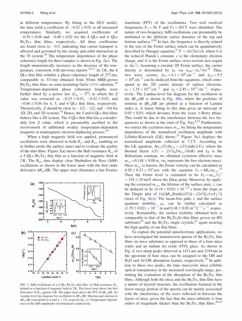
at different temperatures. By fitting to the HLN model,
the data yield a coefficient of �0.52 6 0.01 at all measured
temperatures. Similarly, we acquired coefficients of
�0.39 6 0.04 and �0.40 6 0.02 for the 4 QLs and 6 QLs
Bi2Te3 thin films, respectively. All three coefficients
are found close to �0.5, indicating that carrier transport is
affected and governed by the strong spin-orbit interaction in
the TI system.16 The temperature dependence of the phase
coherence length for three samples is shown in Fig. 2(c). The
length monotonically increases as the decrease of the tem-
perature, consistent with previous reports.14,17 At 2 K, the 6
QLs thin film exhibits a phase coherence length of 277 nm,
comparable to 331 nm obtained from 50 nm MBE-grown
Bi2Te3 thin films on semi-insulating GaAs (111) substrate.18
Temperature-dependent phase coherence lengths were
further fitted by a power law (L/ � Tb) in which the bvalue was extracted as �0.25 6 0.03, �0.42 6 0.03, and
�0.66 6 0.04 for 4, 5, and 6 QLs thin films, respectively.
Theoretically, b should be close to �1/3, �1/2, and �3/4 for
1D, 2D, and 3D systems.18 Hence, the 5 and 6 QLs thin films
behave like a 2D system. The 4 QLs thin film has a consider-
ably low b value, which is presumably ascribed to the
involvement of additional weakly temperature-dependent
magnetic or nonmagnetic electron dephasing process.19
When a high magnetic field was applied, pronounced
oscillations were observed in both Rxx and Ryx, enabling us
to further probe the surface states and to evaluate the quality
of the thin films. Figure 3(a) shows the Hall resistance Ryx of
a 4 QLs Bi2Te3 thin film as a function of magnetic field at
2 K. The Ryx data display clear Shubnikov-de Hass (SdH)
oscillations as shown in the lower inset with the first order
derivative dRyx/dB. The upper inset illustrates a fast Fourier
transform (FFT) of the oscillations. Two well resolved
frequencies F1¼ 56 T and F2¼ 101 T were identified. The
nature of two-frequency SdH oscillations can presumably be
attributed to the different carrier densities of the top and
bottom surfaces.4,20 In fact, the frequency is directly related
to the size of the Fermi surface which can be quantitatively
described by Onsager equation,21 F ¼ (�h/(2pe))A, where �h is
the reduced Planck’s constant, e is the elementary electron
charge, and A is the Fermi surface cross-section area (equal
to pkF2). Assuming a circular 2D Fermi surface, the carrier
density is determined by kF via n2D¼ kF2/4p.22 Thus,
two wave vectors, kF1¼ 4.1� 106 cm�1 and kF2¼ 5.5
� 106 cm�1 can be deduced from the equations, which corre-
spond to the 2D carrier density of surface electrons,
n1¼ 1.35� 1012 cm�2 and n2¼ 2.45� 1012 cm�2, respec-
tively. The Landau-level fan diagram for the oscillation in
the dRyx/dB is shown in Fig. 3(b), where the positions of
minima in dRyx/dB are plotted as a function of Landau
index n. A linear fitting to this data gives an intercept of
0.65 6 0.03, which deviates from the exact p-Berry phase.
This could be due to the interference between the two fre-
quencies as shown in the inset of Fig. 3(a).6,23 Furthermore,
we extract the cyclotron mass mcyc by fitting the temperature
dependence of the normalized oscillation amplitude with
Lifshitz-Kosevich (LK) theory.21 Figure 3(c) displays the
normalized amplitude collected at 7.2 T. According to
the LK equation, Drxx(T)/Drxx¼ k(T)/sinh(k(T)), where the
thermal factor k(T) ¼ 2p2kBTmcyc/(�heB) and kB is the
Boltzmann constant, we obtained cyclotron effective mass
mcyc¼0.148 6 0.08 me (me represents the free electron mass).
Once mcyc is known, the Fermi velocity can be calculated as
4.28 6 0.23� 105 m/s with the equation VF¼ �hKF/mcyc.22
Then the Fermi level is estimated to be EF¼mcycVF2
¼ 154 6 25 meV above the Dirac point. Moreover, by apply-
ing the extracted mcyc, the lifetime of the surface state, s, can
be deduced to be (4.18 6 0.02)� 10�13 s from the slope in
the Dingle plot of Ln[DRxxBsinh(k(T))]� [2p2EF/(seVF2)]
(inset of Fig. 3(c)). The mean-free path, l, and the surface
quantum mobility, ls, can be further calculated as
(1.79 6 0.02) � 10�7 m and 0.48 6 0.03 m2 V�1 s�1, respec-
tively. Remarkably, the surface mobility obtained here is
comparable to that of the Bi2Te2Se thin films grown on BN
substrates24 and the Bi2Te3 single crystals,22 again assuring
the high quality of our thin films.
To explore the potential optoelectronic applications, we
have investigated the transmission spectra of the Bi2Te3 thin
films on mica substrates as opposed to those of a bare mica
wafer and an indium tin oxide (ITO) glass. As shown in
Fig. 4, two sharp peaks observed at 1421 nm and 2194 nm in
the spectrum of bare mica can be assigned to the OH and
H2O and Al-OH absorption feature, respectively.25 In addi-
tion to these two peaks, the bare muscovite mica exhibits
optical transparency in the measured wavelength range, per-
mitting the evaluation of the absorption of the Bi2Te3 thin
films. Although both the mica and the Bi2Te3 thin film have
a nature of layered structure, the oscillations featured in the
lower energy portion of the spectra can be mainly associated
with the interference of the wave reflected in between the
layers of mica, given the fact that the mica substrate is four
orders of magnitude thicker than the Bi2Te3 thin films.26,27
FIG. 3. SdH oscillations of a 4 QLs Bi2Te3 thin film. (a) Hall resistance Ryx
plotted as a function of magnetic field at 2 K. The lower inset shows the first
derivative of Ryx against 1/B. The upper inset shows the FFT of dRyx/dB. (b)
Landau level fan diagram for oscillation in dRyx/dB. Maxima and minima in
dRyx/dB correspond to n and n þ 1/2, respectively. (c) Temperature depend-
ence of the SdH amplitudes of normalized conductivity.
031605-3 Wang et al. Appl. Phys. Lett. 103, 031605 (2013)

The absorption of Bi2Te3 thin films manifests evident
thickness-dependent features in the entire wavelength range.
Significantly, 4 QLs and 15 QLs Bi2Te3 thin films have an
average visible transmittance of �45% and �10%, respec-
tively, suggesting the high absorbance of the Bi2Te3 thin
films. Moreover, similar to Bi2Se3 nanosheets on mica,27 our
ultrathin Bi2Te3 film exhibits a superior transmittance in
range of 1200–2500 nm compared with ITO glass. These
unique optical features of our Bi2Te3 thin films, together
with the robust surface sates, provide a possibility to realize
high-performance optoelectronics in specific spectrum
ranges.
To summarize, high-quality Bi2Te3 thin films exhibiting
atomically smooth terraces over several microns have been
fabricated on insulating and flexible mica substrates by MBE.
The relatively large phase coherence length of relatively thin
samples extracted from the WAL effect, and the high mobil-
ity deduced by the quantum oscillations can be attributed to
the reduced defect density epilayer grown by means of
vdWE. The availability of such high quality TI thin films on
the transparent mica substrates will facilitate the investigation
of the quantum interference effect and the manipulation of
the surface states, providing the possibility of exploring the
potential application of TI in optoelectronics.
This work was supported by the National Young 1000
Talents Plan in China. N. Meyer and X. Y. Che would like to
thank the financial support from the U.S. National Science
Foundation under the Award No. 1201883.
1X. L. Qi and S. C. Zhang, Rev. Mod. Phys. 83, 1057 (2011); J. E. Moore,
Nature 464, 194 (2010); O. V. Yazyev, J. E. Moore, and S. G. Louie,
Phys. Rev. Lett. 105, 266806 (2010); V. Goyal, D. Teweldebrhan, and
A. A. Balandin, Appl. Phys. Lett. 97, 133117 (2010).2S. S. Hong, J. J. Cha, D. S. Kong, and Y. Cui, Nat. Commun. 3, 757
(2012).
3H. D. Li, Z. Y. Wang, X. Kan, X. Guo, H. T. He, Z. Wang, J. N. Wang,
T. L. Wong, N. Wang, and M. H. Xie, New J. Phys. 12, 103038 (2010);
M. L. Teague, H. Chu, F. X. Xiu, L. He, K. L. Wang, and N. C. Yeh, Solid
State Commun. 152, 747 (2012).4A. A. Taskin, S. Sasaki, K. Segawa, and Y. Ando, Adv. Mater. 24, 5581
(2012).5S. Schreyeck, N. V. Tarakina, G. Karczewski, C. Schumacher,
T. Borzenko, C. Brune, H. Buhmann, C. Gould, K. Brunner, and L. W.
Molenkamp, Appl. Phys. Lett. 102, 041914 (2013).6Z. Ren, A. A. Taskin, S. Sasaki, K. Segawa, and Y. Ando, Phys. Rev. B
85, 155301 (2012).7A. Koma, Thin Solid Films 216, 72 (1992).8Y. S. Zhou, K. Wang, W. H. Han, S. C. Rai, Y. Zhang, Y. Ding, C. F. Pan,
F. Zhang, W. L. Zhou, and Z. L. Wang, ACS Nano 6, 6478 (2012); J. D.
Grunwaldt, F. Atamny, U. Gobel, and A. Baiker, Appl. Surf. Sci. 99, 353
(1996); M. I. B. Utama, F. J. Belarre, C. Magen, B. Peng, J. Arbiol, and
Q. H. Xiong, Nano Lett. 12, 2146 (2012).9Y. Y. Li, G. A. Wang, X. G. Zhu, M. H. Liu, C. Ye, X. Chen, Y. Y. Wang,
K. He, L. L. Wang, X. C. Ma, H. J. Zhang, X. Dai, Z. Fang, X. C. Xie,
Y. Liu, X. L. Qi, J. F. Jia, S. C. Zhang, and Q. K. Xue, Adv. Mater. 22,
4002 (2010).10N. Bansal, Y. S. Kim, M. Brahlek, E. Edrey, and S. Oh, Phys. Rev. Lett.
109, 116804 (2012).11X. X. Yu, L. He, M. R. Lang, W. J. Jiang, F. X. Xiu, Z. M. Liao, Y. Wang,
X. F. Kou, P. Zhang, J. S. Tang, G. Huang, J. Zou, and K. L. Wang,
Nanotechnology 24, 015705 (2013).12Y. Liu, M. Weinert, and L. Li, Phys. Rev. Lett. 108, 115501 (2012); M. X.
Wang, C. H. Liu, J. P. Xu, F. Yang, L. Miao, M. Y. Yao, C. L. Gao, C. Y.
Shen, X. C. Ma, X. Chen, Z. A. Xu, Y. Liu, S. C. Zhang, D. Qian, J. F. Jia,
and Q. K. Xue, Science 336, 52 (2012).13V. Russo, A. Bailini, M. Zamboni, M. Passoni, C. Conti, C. S. Casari,
A. L. Bassi, and C. E. Bottani, J. Raman Spectrosc. 39, 205 (2008); H. L.
Cao, R. Venkatasubramanian, C. Liu, J. Pierce, H. R. Yang, M. Z. Hasan,
Y. Wu, and Y. P. Chen, Appl. Phys. Lett. 101, 162104 (2012); X. Liu,
D. J. Smith, J. Fan, Y. H. Zhang, H. Cao, Y. P. Chen, J. Leiner, B. J.
Kirby, M. Dobrowolska, and J. K. Furdyna, ibid. 99, 171903 (2011).14S. Matsuo, T. Koyama, K. Shimamura, T. Arakawa, Y. Nishihara,
D. Chiba, K. Kobayashi, T. Ono, C. Z. Chang, K. He, X. C. Ma, and Q. K.
Xue, Phys. Rev. B 85, 075440 (2012).15S. Hikami, A. I. Larkin, and Y. Nagaoka, Prog. Theor. Phys. 63, 707
(1980).16H. Steinberg, J. B. Lalo€e, V. Fatemi, J. S. Moodera, and P. Jarillo-Herrero,
Phys. Rev. B 84, 233101 (2011).17L. H. Bao, L. He, N. Meyer, X. F. Kou, P. Zhang, Z. G. Chen, A. V.
Fedorov, J. Zou, T. M. Riedemann, T. A. Lograsso, K. L. Wang, G. Tuttle,
and F. X. Xiu, Sci. Rep. 2, 726 (2012).18H. T. He, G. Wang, T. Zhang, I. K. Sou, G. K. L. Wong, J. N. Wang, H. Z.
Lu, S. Q. Shen, and F. C. Zhang, Phys. Rev. Lett. 106, 166805 (2011).19S. P. Chiu and J. J. Lin, Phys. Rev. B 87, 035122 (2013).20A. A. Taskin, S. Sasaki, K. Segawa, and Y. Ando, Phys. Rev. Lett. 109,
066803 (2012).21D. Shoenberg, Magnetic Oscillations in Metals (Cambridge University
Press, 1984).22D. X. Qu, Y. S. Hor, J. Xiong, R. J. Cava, and N. P. Ong, Science 329, 821
(2010).23L. Fang, Y. Jia, D. J. Miller, M. L. Latimer, Z. L. Xiao, U. Welp, G. W.
Crabtree, and W. K. Kwok, Nano Lett. 12, 6164 (2012).24P. Gehring, B. F. Gao, M. Burghard, and K. Kern, Nano Lett. 12, 5137
(2012).25W. Herrmann, M. Blake, M. Doyle, D. Huston, J. Kamprad, N. Merry, and
S. Pontual, Econ. Geol. 96, 939 (2001).26M. I. B. Utama, Z. P. Peng, R. Chen, B. Peng, X. L. Xu, Y. J. Dong, L. M.
Wong, S. J. Wang, H. D. Sun, and Q. H. Xiong, Nano Lett. 11, 3051
(2011).27H. L. Peng, W. H. Dang, J. Cao, Y. L. Chen, W. Wu, W. S. Zheng, H. Li,
Z. X. Shen, and Z. F. Liu, Nat. Chem. 4, 281 (2012).
FIG. 4. UV-Vis-NIR spectra of Bi2Te3 thin films with different thicknesses
on mica.
031605-4 Wang et al. Appl. Phys. Lett. 103, 031605 (2013)