Embed Size (px)
Citation preview

Amorphous and HeterogeneousSilicon-Based Films—2001
www.cambridge.org© in this web service Cambridge University Press
Cambridge University Press978-1-107-41224-8 - Materials Research Society Symposium Proceedings: Volume 664:Amorphous and Heterogeneous Silicon-Based Films—2001Editors: Martin Stutzmann, James B. Boyce, J. David Cohen, Robert W. Collinsand Jun-ichi HannaFrontmatterMore information
MATERIALS RESEARCH SOCIETYSYMPOSIUM PROCEEDINGS VOLUME 664
Amorphous and HeterogeneousSilicon-Based Films—2001
Symposium held April 16-20, 2001, San Francisco, California, U.S.A.
EDITORS:
Martin StutzmannTechnische Universitat Mtinchen
Garching, Germany
James B. BoyceXerox Palo Alto Research Center
Palo Alto, California, U.S.A.
J. David CohenUniversity of Oregon
Eugene, Oregon, U.S.A.
Robert W. CollinsThe Pennsylvania State University
University Park, Pennsylvania, U.S.A.
Jun-ichi HannaTokyo Institute of Technology
Yokohama, Japan
IMTRISIMaterials Research Society
Warrendale, Pennsylvania
www.cambridge.org© in this web service Cambridge University Press
Cambridge University Press978-1-107-41224-8 - Materials Research Society Symposium Proceedings: Volume 664:Amorphous and Heterogeneous Silicon-Based Films—2001Editors: Martin Stutzmann, James B. Boyce, J. David Cohen, Robert W. Collinsand Jun-ichi HannaFrontmatterMore information

cambridge university press Cambridge, New York, Melbourne, Madrid, Cape Town, Singapore, São Paulo, Delhi, Mexico City
Cambridge University Press32 Avenue of the Americas, New York ny 10013-2473, USA
Published in the United States of America by Cambridge University Press, New York
www.cambridge.orgInformation on this title: www.cambridge.org/9781107412248
Materials Research Society506 Keystone Drive, Warrendale, pa 15086http://www.mrs.org
© Materials Research Society 2001
This publication is in copyright. Subject to statutory exceptionand to the provisions of relevant collective licensing agreements, no reproduction of any part may take place without the written permission of Cambridge University Press.
This publication has been registered with Copyright Clearance Center, Inc.For further information please contact the Copyright Clearance Center,Salem, Massachusetts.
First published 2001 First paperback edition 2013
Single article reprints from this publication are available throughUniversity Microfilms Inc., 300 North Zeeb Road, Ann Arbor, mi 48106
CODEN: MRSPDH
isbn 978-1-107-41224-8 Paperback
Cambridge University Press has no responsibility for the persistence oraccuracy of URLs for external or third-party internet websites referred to inthis publication, and does not guarantee that any content on such websites is,or will remain, accurate or appropriate.
www.cambridge.org© in this web service Cambridge University Press
Cambridge University Press978-1-107-41224-8 - Materials Research Society Symposium Proceedings: Volume 664:Amorphous and Heterogeneous Silicon-Based Films—2001Editors: Martin Stutzmann, James B. Boyce, J. David Cohen, Robert W. Collinsand Jun-ichi HannaFrontmatterMore information

CONTENTS
Preface xxi
Materials Research Society Symposium Proceedings xxiii
NUCLEATIONAND GROWTH
f In Situ Probing and Atomistic Simulation of a-Si:H PlasmaDeposition Al.l
Eray S. Aydil, Dimitrios Maroudas, Denise C. Marra,W.M.M. Kessels, Sumit Agarwal, Shyam Ramalingam,Saravanapriyan Sriraman, M.C.M. Van de Sanden, and Akihiro Takano
Effect of Strained Si-Si Bonds in Amorphous Silicon IncubationLayer on Microcrystalline Silicon Nucleation A1.2
Hiroyuki Fujiwara, Michio Kondo, and Akihisa Matsuda
Quantitative Modeling of Nucleation Kinetics in Experiments forPoly-Si Growth on SiO2 by Hot-Wire Chemical Vapor Deposition A1.3
Maribeth Swiatek, Jason K. Holt, and Harry A. Atwater
Thermodynamic Model of the Role of Hydrogen Dilution inPlasma Deposition of Microcrystalline Silicon A1.5
J. Robertson
NOVEL CONCEPTS
Photovoltaics on Wire A2.1M. Rojahn, M. Rakhlin, and M.B. Schubert
HOTWIRECVDI
Identification of Growth Precursors in Hot Wire CVD ofAmorphous Silicon Films A3.1
H.L. Duan, G.A. Zaharias, and Stacey F. Bent
Radical Species Distributions in Hot-Wire Chemical VaporDeposition Probed Via Threshold Ionization Mass Spectrometryand Direct Simulation Monte Carlo Techniques A3.2
Jason K. Holt, Maribeth Swiatek, David G. Goodwin,Harry A. Atwater, R.P. Muller, and W.A. Goddard III
* Invited Paper
www.cambridge.org© in this web service Cambridge University Press
Cambridge University Press978-1-107-41224-8 - Materials Research Society Symposium Proceedings: Volume 664:Amorphous and Heterogeneous Silicon-Based Films—2001Editors: Martin Stutzmann, James B. Boyce, J. David Cohen, Robert W. Collinsand Jun-ichi HannaFrontmatterMore information
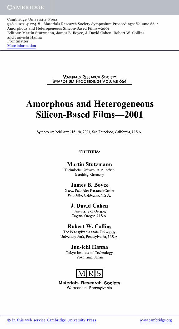
Films and Devices Deposited by HWCVD at Ultra HighDeposition Rates A3.3
A.H. Mahan, Y. Xu, E. Iwaniczko, D.L. Williamson, W. Beyer,J.D. Perkins, M. Vanecek, L.M. Gedvilas, and B.P. Nelson
Structural Characterization of SiF4, SiH4, and H2 Hot-Wire-GrownMicrocrystalline Silicon Thin Films With Large Grains A3.4
JJ. Gutierrez, C.E. Inglefield, C.P. An, M.C. DeLong,P.C. Taylor, S. Morrison, and A. Madan
T-Site Trapped Molecular Hydrogen in Hot Wire a-Si:H A3.5J. Herberg, P.A. Fedders, DJ. Leopold, R.E. Norberg, and R.E. Schropp
p-Type Window Layers for pin Solar Cells Entirely Fabricated byHot-WireCVD A3.6
Urban Weber, Markus Koob, Chandrachur Mukherjee,D. Chandrashekhar, Rajiv O. Dusane, and Bernd Schroeder
HIGH RA TE DEPOSITION
Material Properties and Growth Process of MicrocrystallineSilicon With Growth Rates in Excess of 1 nm/s A4.2
E.A.G. Hamers, A.H.M. Smets, C. Smit, J.P.M. Hoefnagels,W.M.M. Kessels, and M.C.M. van de Sanden
* High Rate Growth of Device Grade Silicon Thin Films for SolarCells A4.3
M. Kondo, S. Suzuki, Y. Nasuno, and A. Matsuda
Evaluation of Microcrystalline Silicon Films Deposited byUltrafast Thermal Plasma CVD A4.4
Yongkee Chae, Hiromasa Ohno, Keisuke Eguchi,and Toyonobu Yoshida
Properties of Large Grain-Size Poly-Si Films by CatalyticChemical Sputtering A4.5
Atsushi Masuda, Koji Kamesaki, Akira Izumi,and Hideki Matsumura
GROWTH OF SILICON ANDSILICON-ALLOY THIN FILMS
Optical Emission Spectroscopy of Germane Plasma Produced inan ECR Reactor A5.2
Matt deFreese, Vikram L. Dalai, and Julie Falter
* Invited Paper
www.cambridge.org© in this web service Cambridge University Press
Cambridge University Press978-1-107-41224-8 - Materials Research Society Symposium Proceedings: Volume 664:Amorphous and Heterogeneous Silicon-Based Films—2001Editors: Martin Stutzmann, James B. Boyce, J. David Cohen, Robert W. Collinsand Jun-ichi HannaFrontmatterMore information

Some Considerations Relating to Growth Chemistry ofAmorphous Si and (Si,Ge) Films and Devices A5.3
Vikram L. Dalai
Phase Diagrams for the Optimization of rf Plasma EnhancedChemical Vapor Deposition of a-Si:H: Variations in PlasmaPower and Substrate Temperature A5.4
Andre S. Ferlauto, Randy J. Koval, Christopher R. Wronski,and Robert W. Collins
VHF Large Area Plasma Processing on Moving Substrates A5.5J. Kuske, U. Stephan, R. Terasa, H. Brechtel, and A. Kottwitz
Cluster-Less Plasma CVD Reactor and Its Application to a-Si:HFilm Deposition A5.6
Masaharu Shiratani, Kazunori Koga, and Yukio Watanabe
Ion-Assisted Sputter Deposition of Microcrystalline Silicon FilmsWith Pulsed-DC Plasma Excitation A5.7
P. Reinig, F. Fenske, B. Selle, and W. Fuhs
The Properties of Low Hydrogen Silicon Thin Films Deposited byMesh-Type PECVD A5.8
Se-won Ryu, Do-Hyun Kwon, Sung-Gye Park,and Hyoung-June Kim
Low-Temperature (630°C) Epitaxy of Silicon on Seeded Glass byIon-Assisted Deposition A5.ll
Armin G. Aberle, Nils-Peter Harder, and Stefan Oelting
CRYSTALLIZATION
Formation of Polycrystalline Silicon Films Using Electrical-Current-Induced Joule Heating A6.2
Nobuyuki Andoh, Hiroyuki Takahashi, and Toshiyuki Sameshima
Electrical Properties of Solid Phase Crystallized Silicon Films A6.3Tadashi Watanabe, Hajime Watakabe, and Toshiyuki Sameshima
Super Poly-Si and Transistor Formed by Nickel-Induced-Lateral-Crystallization A6.4
C.F. Cheng, T.C. Leung, and M.C. Poon
A Novel Back-Reflecting UV-Assisted Metal-InducedCrystallization of Silicon on Glass A6.5
Leila Rezaee, Shamsoddin Mohajerzadeh, Ali Khakiflrooz,Saber Haji, and Ebrahim Asl Soleimani
vn
www.cambridge.org© in this web service Cambridge University Press
Cambridge University Press978-1-107-41224-8 - Materials Research Society Symposium Proceedings: Volume 664:Amorphous and Heterogeneous Silicon-Based Films—2001Editors: Martin Stutzmann, James B. Boyce, J. David Cohen, Robert W. Collinsand Jun-ichi HannaFrontmatterMore information

A New Field-Aided Germanium-Induced Lateral Crystallizationof Silicon A6.6
Kianoush Naeli, Shamsoddin Mohajerzadeh, Ali Khakifirooz,Saber Haji, and Ebrahim A. Soleimani
Directional Field Aided Lateral Crystallization of AmorphousSilicon Thin Films A6.7
Marek A.T. Izmajlowicz, Neil A. Morrison, Andrew J. Flewitt,and William I. Milne
The Effects of Cu on Field Aided Lateral Crystallization (FALC)of Amorphous Silicon (a-Si) Films A6.8
Jae-Bok Lee, Chul-Ho Kim, Se-Youl Kwon, and Duck-Kyun Choi
CW Argon-Ion Laser Crystallization of a-Si:H Thin Films A6.9A. Sunda-Meya, D. Gracin, J. Dutta, B. Vlahovic,and RJ. Nemanich
Electrical Properties and Defect States of Laser CrystallizedPolycrystalline Silicon Films A6.10
Tadashi Watanabe, Nobuyuki Andoh, and Toshiyuki Sameshima
Excimer Laser Recrystallization of Selectively Floating a-Si ActiveLayer for Large-Grained Poly-Si Film A6.ll
Cheon-Hong Kim, Juhn-Suk Yoo, In-Hyuk Song, and Min-Koo Han
HOT WIRE CVDII
The Effect of H2 Dilution on Thin Film SiN Deposited by Hot WireCVD Using SiH4 and NH3 Gas Mixtures A7.2
A.C. Dillon, L. Gedvillas, D.L. Williamson, J. Thiesen,J.D. Perkins, and A.H. Mahan
The Effect of Moderate Hydrogen Dilution on Stability andStructure of Amorphous Silicon Deposited by Hot-Wire CVD A7.3
Urban Weber and Bernd Schroeder
Large Red Shift of PL Peak Energy in High Growth Rate a-Si:HPrepared by Hot-Wire CVD A7.4
Daxing Han, Guozhen Yue, Jennifer Weinberg-Wolf,Jessica M. Owens, Yueqin Xu, and Qi Wang
High Quality Amorphous Silicon Germanium Alloy Solar CellsMade by Hot-Wire CVD at 10 A/s A7.5
Qi Wang, Eugene Iwaniczko, Jeffrey Yang, Kenneth Lord,and Subhendu Guha
Vlll
www.cambridge.org© in this web service Cambridge University Press
Cambridge University Press978-1-107-41224-8 - Materials Research Society Symposium Proceedings: Volume 664:Amorphous and Heterogeneous Silicon-Based Films—2001Editors: Martin Stutzmann, James B. Boyce, J. David Cohen, Robert W. Collinsand Jun-ichi HannaFrontmatterMore information

Properties of Nanocrystalline n-Type Silicon Films Produced byHot Wire Plasma Assisted Technique..... A7.6
I. Ferreira, F. Braz Fernandes, P. Vilarinho, E. Fortunato, andR. Martins
SILICON-BASED ALLOYS
Stress Induced Lateral Concentration Profiles in SiGe LayersGrown on Si(OOl) Non-Planar Substrates A8.3
Anat Eshed, Robert Beserman, and Klauss Dettmer
Electronic and Optical Properties of High Quality Low BandgapAmorphous (Ge, Si) Alloys A8.4
S.R. Sheng, R. Braunstein, and V.L. Dalai
Hydrogen Concentration Analysis in PECVD and RTCVD SiliconNitride Thin Films and Its Impact on Device Performance A8.5
C.Y. Wang, E.H. Lim, H. Liu, J.L. Sudijono, T.C. Ang,V.Y. Vassiliev, and J.Z. Zheng
High-Rate Deposition of a-SiNx:H Films for PhotovoltaicApplications A8.6
W.M.M. Kessels, F.J.H. van Assche, J. Hong, J.D. Moschner,T. Lauinger, D.C. Schram, and M.C.M. van de Sanden
Thermal Annealing Study of Variable Bandgap a-SiN:H Alloy Films A8.7N. Banerji, E. Faro, and J. Serra
Ge Island Evolution During Growth, In Situ Anneal, andSi Capping in an Industrial CVD Reactor A8.8
Roger Loo, Philippe Meunier-Beillard, Didier Dentel,Michael Goryll, Danielle Vanhaeren, Lili Vescan, Hugo Bender,Matty Caymax, and Wilfried Vandervorst
STRUCTURAL PROPERTIES OFHETEROGENEOUS SILICON FILMS
Microstructure Characterization of Hydrogenated AmorphousSilicon Films by Rare Gas Effusion Studies A9.2
Wolfhard Beyer
Stability and Nanostructure of Heterogeneous Amorphous SiliconThin-Film Synthesized Under High Chamber Pressure (500 to2200 mTorr) Regime of RF PECVD A9.5
A.R. Middya, S. Hamma, S. Hazra, S. Ray, and C. Longeaud
www.cambridge.org© in this web service Cambridge University Press
Cambridge University Press978-1-107-41224-8 - Materials Research Society Symposium Proceedings: Volume 664:Amorphous and Heterogeneous Silicon-Based Films—2001Editors: Martin Stutzmann, James B. Boyce, J. David Cohen, Robert W. Collinsand Jun-ichi HannaFrontmatterMore information

Nanostructured Silicon Films Produced by PECVD A9.6R. Martins, H. Aguas, V. Silva, I. Ferreira, A. Cabrita,and E. Fortunato
Effects of Hydrogen Dilution on a-Si:H and Its Solar Cells Studiedby Raman and Photoluminescence Spectroscopy A9.7
Guozhen Yue, Jessica M. Owens, Jennifer Weinberg-Wolf,Daxing Han, Jeffrey Yang, Kenneth Lord, Baojie Yan,and Subhendu Guha
Morphology, Phonon Confinement and Properties of a-Si:H Films A9.8Valeri Ligatchev
DOPANTS AND IMPURITIES
Where Oxygen Donor Lives in Microcrystalline Silicon A10.1Toshihiro Kamei, Takehito Wada, and Akihisa Matsuda
Relation Between Erbium Photoluminescence and Dangling-BondDefects in a-Si:H , A10.4
Minoru Kumeda, Hiroshi Itoh, Norio Shitakata,and Tatsuo Shimizu
AMORPHOUS SILICONSOLAR CELLS
* Towards Stabilized 10% Efficiency of Large-Area (> 5000cm2)a-Si/a-SiGe Tandem Solar Cells Using High-Rate Deposition All . l
Shingo Okamoto, Akira Terakawa, Eiji Maruyama,Wataru Shinohara, Makoto Tanaka, and Seiichi Kiyama
Higher Efficiency of n-i-p Solar Cells by Hot-Wire CVD atModerate Temperatures A11.2
Marieke K. van Veen and Ruud E.I. Schropp
Amorphous Silicon and Silicon Germanium Alloy Solar CellsDeposited by VHF at High Rates A11.3
Jeffrey Yang, Baojie Yan, Jozef Smeets, and Subhendu Guha
* Technology Transfer Challenges in the Manufacturing of a-SiTandem Solar Cells A11.4
D.E. Carlson, G. Ganguly, G. Lin, M. Gleaton, M. Bennett,and R.R. Arya
* Invited Paper
www.cambridge.org© in this web service Cambridge University Press
Cambridge University Press978-1-107-41224-8 - Materials Research Society Symposium Proceedings: Volume 664:Amorphous and Heterogeneous Silicon-Based Films—2001Editors: Martin Stutzmann, James B. Boyce, J. David Cohen, Robert W. Collinsand Jun-ichi HannaFrontmatterMore information

METASTABILITY I
Photocarrier Capture Properties of Light-Induced Defects in a-Si:H A12.1Paul Stradins, Satoshi Shimizu, Michio Kondo, and Akihisa Matsuda
New Experiments on the Relationship Between Light-InducedDefects and Photoconductivity Degradation A12.2
Stephan Heck and Howard M. Branz
Contributions of D° and Non-D° Gap States to the Kinetics ofLight Induced Degradation of Amorphous Silicon Under 1 sunIllumination A12.3
J. Pearce, X. Niu, R. Koval, G. Ganguly, D. Carlson,R.W. Collins, and C.R. Wronski
Light-Induced Creation of Defects and Lifetime Distribution ofPhotoluminescence in a-Si:H Based Films A12.4
Chisato Ogihara, Hitoshi Takemura, and Kazuo Morigaki
Light-Induced Annealing of Deep Defects in Low Ge Fractiona-Si,Ge:H Alloys: Further Insights Into the Fundamentals ofLight-Induced Degradation A12.5
J. David Cohen, Jennifer Heath, Kimon C. Palinginis,Jeffrey C. Yang, and Subhendu Guha
Changes in Hydrogenated Amorphous Silicon Upon ExtensiveLight-Soaking at Elevated Temperature A12.6
N. Hata, CM. Fortmann, and A. Matsuda
HYDROGENANDMETASTABILITY
* Diffusion and Solubility of Hydrogen in Amorphous andMicrocrystalline Si:H Films A13.1
Wolfhard Beyer
* Forms of Hydrogen and Hydrogen Diffusion in Realistic Modelsofa-Si:H A13.2
P.A. Fedders
* Hydrogen Equilibration and Metastability in Amorphous Silicon A13.3Howard M. Branz and S.B. Zhang
* Invited Paper
XI
www.cambridge.org© in this web service Cambridge University Press
Cambridge University Press978-1-107-41224-8 - Materials Research Society Symposium Proceedings: Volume 664:Amorphous and Heterogeneous Silicon-Based Films—2001Editors: Martin Stutzmann, James B. Boyce, J. David Cohen, Robert W. Collinsand Jun-ichi HannaFrontmatterMore information

METASTABILITYII
Network Rebonding Model for Metastability in AmorphousSilicon A14.1
R. Biswas, B.C. Pan, and Y. Ye
Investigation of Light-Induced Defect Depth Profile inHydrogenated Amorphous Silicon Films A14.2
S. Shimizu, P. Stradins, M. Kondo, and A. Matsuda
Illumination- and Annealing-Induced Changes in the Infrared andRaman Spectra of a-Si:H A14.3
L.-F. Arsenault, S. Lebib, E. Sacher, and A. Yelon
Is Interstitial Hydrogen Playing a Role in the Staebler-WronskiEffect? A14.4
C. Longeaud and D. Roy
The Staebler-Wronski Effect and 1/f Noise in Amorphous Silicon A14.5T. J. Belich and J. Kakalios
Defect Creation by Electron Beam Irradiation in AmorphousSilicon Nitride Films Compared With That by Light Soaking A14.6
Tatsuo Shimizu, Yuji Kawashima, and Minoru Kumeda
MICROCRYSTALLINE SILICONSOLAR CELLS
Assessment of the Use of Microcrystalline Silicon MaterialsGrown at Rates Near 15 A/s as i-Layer Material for Single andMulti-Junction Solar Cells A15.1
S.J. Jones, R. Crucet, R. Capangpangan, M. Izu, and A. Banerjee
Structural Properties of Microcrystalline Si Solar Cells A15.2M. Luysberg, C. Scholten, L. Houben, R. Carius, F. Finger,and O. Vetterl
Improved Interface Between Front TCO and MicrocrystallineSilicon p-i-n Solar Cells A15.3
E. Vallat-Sauvain, S. Fay, S. Dubail, J. Meier, J. Bailat, U. Kroll,and A. Shah
Tailoring the Structure of Low-Temperature-DepositedMicrocrystalline Silicon Films by Biasing the Substrate A15.4
Mario Birkholz, Burkhardt Selle, Walther Funs,and Don L. Williamson
xn
www.cambridge.org© in this web service Cambridge University Press
Cambridge University Press978-1-107-41224-8 - Materials Research Society Symposium Proceedings: Volume 664:Amorphous and Heterogeneous Silicon-Based Films—2001Editors: Martin Stutzmann, James B. Boyce, J. David Cohen, Robert W. Collinsand Jun-ichi HannaFrontmatterMore information

* Microcrystalline Silicon Thin-Film Solar Cells Prepared at LowTemperature A15.5
Y. Nasuno, M. Kondo, and A. Matsuda
Thin Film a-Si/poly-Si Multibandgap Tandem Solar Cells WithBoth Absorber Layers Deposited by Hot Wire CVD A15.6
R.E.I. Schropp, C.H.M. Van Der Werf, M.K. Van Veen,P.A.T.T. Van Veenendaal, R. Jimenez Zambrano, Z. Hartman,J. Loftier, and J.K. Rath
TRANSPORT IN fjc-Si
* Microscopic Aspects of Charge Transport in HydrogenatedMicrocrystalline Silicon A16.1
Antonin Fejfar, Tomas Mates, Christian Koch, Bohuslav Rezek,Vladimir Svrcek, Petr Fojtik, Ha Stuchlikova, Jiri Stuchlik,and Jan Kocka
Carrier Transport in Ultra-Thin Nano/Polycrystalline SiliconFilms andNanowires A16.2
Toshio Kamiya, Yong T. Tan, Yoshikazu Furuta,Hiroshi Mizuta, Zahid A.K. Durrani, and Haroon Ahmed
Improvement in Electrical Properties of Polycrystalline SiliconFilms by the H2O Vapor Annealing Method A16.3
Toshiyuki Sameshima, Katsumi Asada, Yoshiyuki Tsunoda,and Yoshiyasu Kaneko
Evolution of the Mobility Gap With Thickness in Hydrogen-Diluted Intrinsic Si:H Materials in the Phase Transition Regionand Its Effect on p-i-n Solar Cell Characteristics A16.4
R.J. Koval, J.M. Pearce, A.S. Ferlauto, R.W. Collins,and C.R. Wronski
Femtosecond Carrier Dynamics in Nanocrystalline Silicon Films:The Effect of the Degree of Crystallinity A16.5
K.E. Myers, Q. Wang, and S.L. Dexheimer
THIN FILM TRANSISTORS
P-Channel Polycrystalline Silicon Thin Film Transistors on SteelFoil Substrates A17.2
Ming Wu and Sigurd Wagner
* Invited Paper
www.cambridge.org© in this web service Cambridge University Press
Cambridge University Press978-1-107-41224-8 - Materials Research Society Symposium Proceedings: Volume 664:Amorphous and Heterogeneous Silicon-Based Films—2001Editors: Martin Stutzmann, James B. Boyce, J. David Cohen, Robert W. Collinsand Jun-ichi HannaFrontmatterMore information

Towards an AU-Hot-Wire TFT: Silicon Nitride and AmorphousSilicon Deposited by Hot-Wire Chemical Vapor Deposition A17.3
B. Stannowski, M.K. van Veen, and R.E.I. Schropp
Jet-Printed Fabrication of a-Si:H Thin-Film Transistors andArrays A17.4
W.S. Wong, S. Ready, R. Matusiak, S.D. White, J.-P. Lu,R. Lau, J. Ho, and R.A. Street
Nanocrystalline Silicon TFTs With 50 nm Thick DepositedChannel Layer, 10 cm2/Vs Electron Mobility and 108 On/OffCurrent Ratio A17.5
Robert B. Min and Sigurd Wagner
SENSORS
Two-Dimensional Amorphous Silicon Color Sensor Array A18.1F. Lemmi, M. Mulato, J. Ho, R. Lau, J.P. Lu, and R.A. Street
Design and Modeling of Optical Sensors in Multi-ChannelTechnology A18.2
D. Knipp, H. Stiebig, and P.G. Herzog
Mechanisms of Cross-Talk in Large Area a-Si:H ContinuousImage Sensors A18.4
M. Mulato, J.P. Lu, S.E. Ready, K. Van Schuylenbergh, J. Ho,R. Lau, J.B. Boyce, and R.A. Street
Tailored Laser Scanned Photodiodes (LSP) for Image Recognition A18.5M. Vieira, M. Fernandes, P. Louro, Y. Vygranenko, R. Schwarz,and M. Schubert
Piezoresistive Sensors on Plastic Substrates Using DopedMicrocrystalline Silicon A18.6
P. Alpuim, V. Chu, and J.P. Conde
METASTABILITY III
Model of Hydrogen-Mediated Metastable Changes in aTwo-Domain Amorphous Silicon Network A19.1
Jonathan Baugh and Daxing Han
Defect Density Profiling in Light-Soaked and AnnealedHydrogenated Amorphous Silicon Solar Cells A19.2
Richard S. Crandall, Jeffrey Yang, and Subhendu Guha
xiv
www.cambridge.org© in this web service Cambridge University Press
Cambridge University Press978-1-107-41224-8 - Materials Research Society Symposium Proceedings: Volume 664:Amorphous and Heterogeneous Silicon-Based Films—2001Editors: Martin Stutzmann, James B. Boyce, J. David Cohen, Robert W. Collinsand Jun-ichi HannaFrontmatterMore information

Laplace-Transform Transient Photocurrent Spectroscopy as aProbe of Metastable Defect Distributions in HydrogenatedAmorphous Silicon A19.3
Mariana J. Gueorguieva, Charlie Main, and Steve Reynolds
Hydrogen Distributions and Model Lineshapes of ESR Signals ofDangling Bonds in a-Si:H A19.4
P.A. Fedders
Fast Light-Induced Change in Ellipsometry Spectra ofHydrogenated Amorphous Silicon Measured Through aTransparent Substrate Upon Bias Light Illumination A19.5
N. Hata, CM. Fortmann, and A. Matsuda
Illumination Dependence of Microcrystalline PIN Diodes A19.6Torsten Brammer, Franz Birmans, Mathias Krause,Helmut Stiebig, and Heribert Wagner
Electrical Stability of a-Si:H TFTs Fabricated at 150°C A19.7H. Gleskova and S. Wagner
Structural Changes in Amorphous Silicon Annealed at LowTemperatures A19.9
Branko Pi vac, Pavo Dubcek, Ognjen Milat, and Ivan Zulim
HYDROGENATION ANDOXIDATION
Surface Derivatization of Amorphous Silicon by Grignard Reagents A20.4Takashi Ehara and Arata Maruyama
Photoluminescence Study of Self-Limiting Oxidation inNanocrystalline Silicon Quantum Dots A20.6
Kenta Arai, Junichi Omachi, Katsuhiko Nishiguchi,and Shunri Oda
THEORY AND COMPUTERMODELING
Vibrational Stretching Modes of the Si-H and Si-D Bonds inAmorphous Silicon Nitride A21.5
Shu-Ya Lin
xv
www.cambridge.org© in this web service Cambridge University Press
Cambridge University Press978-1-107-41224-8 - Materials Research Society Symposium Proceedings: Volume 664:Amorphous and Heterogeneous Silicon-Based Films—2001Editors: Martin Stutzmann, James B. Boyce, J. David Cohen, Robert W. Collinsand Jun-ichi HannaFrontmatterMore information

DEFECTS ANDDEFECT SPECTROSCOPY
Sensitization of the Holes Lifetime by the Addition of DanglingBonds in a-Si:H A22.2
L.F. Fonseca, S.Z. Weisz, and I. Balberg
Orientation-Dependence of Low-Temperature Epitaxial SiliconGrowth A22.3
Thomas A. Wagner, Lars Oberbeck, Melanie Nerding,Horst P. Strunk, and Ralf B. Bergmann
Ex Situ and In Situ Defect Density Measurements of a-Si:H byMeans of the Cavity Ring Down Absorption Technique A22.4
A.H.M. Smets, J.H. van Helden, and M.C.M. van de Sanden
Study of Defects in Hydrogenated Amorphous Silicon by ConstantPhotocurrent Method and Positron Annihilation A22.5
A. Amaral, G. Lavareda, C. Nunes de Carvalho, P. Brogueira,P.M. Gordo, V.S. Subrahmanyam, C. Lopes Gil, M. Duarte Naia,and A.P. de Lima
Effect of Experimental Noise on Recovery of the ElectronicDensity of States From Transient Photocurrent Data A22.6
Steve Reynolds, Charlie Main, and Mariana J. Gueorguieva
STRUCTURAL AND ELECTRONICPROPERTIES OF THIN SILICON FILMS
Properties of Silicon Films Deposited Under Argon Dilution A23.1C. Longeaud, D. Roy, P. Chaudhuri, N. Dutta Gupta,P. Pratim Ray, S. Vignoli, R. Meaudre, M. Meaudre,and L. Saviot
The Determination of Optoelectronic Properties of Microcrystallineand Amorphous Silicon Films A23.2
Marinus Kunst, Susanne von Aichberger, Wilhelm Thorn,and Frank Wunsch
Structural and Optical Features of Nanocrystalline Silicon FilmsPrepared by PECVD and rf Magnetron Sputter Techniques A23.3
M.-B. Park and N.-H.Cho
Electronic Transport Study of High Deposition Rate HWCVDa-Si:H by the Microwave Photomixing Technique A23.4
S.R. Sheng, R. Braunstein, B.P. Nelson, and Y. Xu
www.cambridge.org© in this web service Cambridge University Press
Cambridge University Press978-1-107-41224-8 - Materials Research Society Symposium Proceedings: Volume 664:Amorphous and Heterogeneous Silicon-Based Films—2001Editors: Martin Stutzmann, James B. Boyce, J. David Cohen, Robert W. Collinsand Jun-ichi HannaFrontmatterMore information

Study of Electrical Properties of Microcrystalline Silicon FilmsUsing AC Measurements A23.5
Ely A.T. Dirani, Alexandre M. Nardes, Adnei M. Andrade,Fernando J. Fonseca, and Reginaldo Muccillo
Increasing the Dark Conductivity Activation Energy in UndopedMicrocrystalline Silicon by Post-Growth Anneals A23.6
Jong-Hwan Yoon
Generation-Recombination Noise in Amorphous Semiconductors A23.7Charlie Main, Steve Reynolds, and Rashad I. Badran
HETEROJUNCTIONS
Charge Carrier Transport in a-Si:H/c-Si Heterojunctions A24.1Susanne von Aichberger, Frank Wunsch, and Marinus Kunst
Importance of Defect Density Near the p-i Interface for a-Si:HSolar Cell Performance A24.4
B.A. Korevaar, C. Smit, R.A.C.M.M. van Swaaij, D.C. Schram,and M.C.M. van de Sanden
Silicon Thin Film Deposition on Nano-Structured ZnO Substrates A24.5R. Konenkamp, V. Chu, J. Conde, and L. Dloczik
Optical Simulations of the Effects of Transparent ConductingOxide Interface Layers on Amorphous Silicon Solar CellPerformance A24.6
Gelio M. Ferreira, Andre S. Ferlauto, Pablo I. Rovira, Chi Chen,Hien V. Nguyen, Christopher R. Wronski, and Robert W. Collins
AMORPHOUS ANDMICROCRYSTALLINE SOLAR CELLS
Integrated Optical and Electrical Modeling of a-Si:H Based SolarCells A25.1
Miro Zeman, Rene A.C.M.M. van Swaaij, Joost J.G. van den Heuvel,and Wim Metselaar
Annealing Kinetics of Amorphous Silicon Alloy Solar Cells Madeat Various Deposition Rates A25.2
Baojie Yan, Jeffrey Yang, Kenneth Lord, and Subhendu Guha
Correlation Between Film and Cell Properties for DC PlasmaDeposited Amorphous Silicon A25.3
Jennifer Heath, Suman B. Iyer, Yoram Lubianiker,J. David Cohen, and Gautam Ganguly
xvii
www.cambridge.org© in this web service Cambridge University Press
Cambridge University Press978-1-107-41224-8 - Materials Research Society Symposium Proceedings: Volume 664:Amorphous and Heterogeneous Silicon-Based Films—2001Editors: Martin Stutzmann, James B. Boyce, J. David Cohen, Robert W. Collinsand Jun-ichi HannaFrontmatterMore information
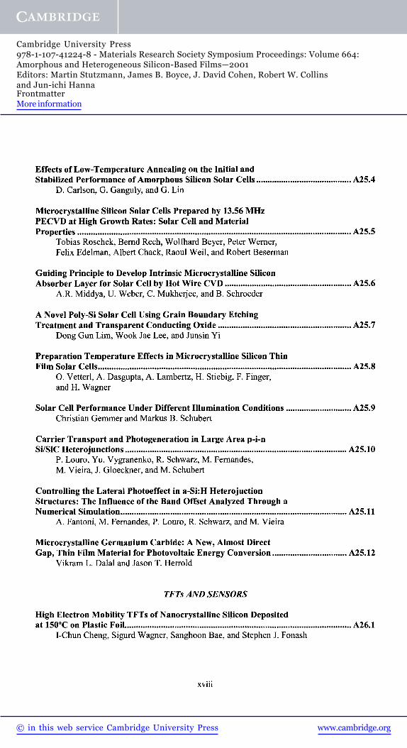
Effects of Low-Temperature Annealing on the Initial andStabilized Performance of Amorphous Silicon Solar Cells A25.4
D. Carlson, G. Ganguly, and G. Lin
Microcrystalline Silicon Solar Cells Prepared by 13.56 MHzPECVD at High Growth Rates: Solar Cell and MaterialProperties A25.5
Tobias Roschek, Bernd Rech, Wolfhard Beyer, Peter Werner,Felix Edelman, Albert Chack, Raoul Weil, and Robert Beserman
Guiding Principle to Develop Intrinsic Microcrystalline SiliconAbsorber Layer for Solar Cell by Hot Wire CVD A25.6
A.R. Middya, U. Weber, C. Mukherjee, and B. Schroeder
A Novel Poly-Si Solar Cell Using Grain Boundary EtchingTreatment and Transparent Conducting Oxide A25.7
Dong Gun Lim, Wook Jae Lee, and Junsin Yi
Preparation Temperature Effects in Microcrystalline Silicon ThinFilm Solar Cells A25.8
O. Vetterl, A. Dasgupta, A. Lambertz, H. Stiebig, F. Finger,and H. Wagner
Solar Cell Performance Under Different Illumination Conditions A25.9Christian Gemmer and Markus B. Schubert
Carrier Transport and Photogeneration in Large Area p-i-nSi/SiC Heterojunctions A25.10
P. Louro, Yu. Vygranenko, R. Schwarz, M. Fernandes,M. Vieira, J. Gloeckner, and M. Schubert
Controlling the Lateral Photoeffect in a-Si:H HeterojuctionStructures: The Influence of the Band Offset Analyzed Through aNumerical Simulation A25.ll
A. Fantoni, M. Fernandes, P. Louro, R. Schwarz, and M. Vieira
Microcrystalline Germanium Carbide: A New, Almost DirectGap, Thin Film Material for Photovoltaic Energy Conversion A25.12
Vikram L. Dalai and Jason T. Herrold
TFTs AND SENSORS
High Electron Mobility TFTs of Nanocrystalline Silicon Depositedat 150°C on Plastic Foil A26.1
I-Chun Cheng, Sigurd Wagner, Sanghoon Bae, and Stephen J. Fonash
www.cambridge.org© in this web service Cambridge University Press
Cambridge University Press978-1-107-41224-8 - Materials Research Society Symposium Proceedings: Volume 664:Amorphous and Heterogeneous Silicon-Based Films—2001Editors: Martin Stutzmann, James B. Boyce, J. David Cohen, Robert W. Collinsand Jun-ichi HannaFrontmatterMore information

Density of States in a-Si:H From SCLC and Its Application inModeling a Vertical TFT A26.2
Naser Sedghi and Bill Eccleston
Photocapacitance of Hydrogenated Amorphous SiliconPhototransistors A26.3
D. Caputo, G. de Cesare, F. Lemmi, A. Nascetti, F. Palma,F. Roca, and M. Tucci
Electromechanical Properties of Amorphous and MicrocrystallineSilicon Micromachined Structures A26.4
J. Gaspar, M. Boucinha, V. Chu, and J.P. Conde
Microcrystalline Germanium Photodetectors A26.5M. Krause, H. Stiebig, R. Carius, and H. Wagner
Hydrogenated Amorphous Silicon/ZnO Schottky Heterojunctionfor Position Sensitive Detectors A26.6
H. Aguas, P. Nunes, E. Fortunato, R. Silva, V. Silva,J. Figueiredo, F. Soares, and R. Martins
Porous Silicon Thin Film Gas Sensor A26.7I. Ferreira, E. Fortunato, and R. Martins
AMORPHOUS-TO-MICROCRYSTALLINETRANSITION
Hydrogen Diffusion During Amorphous Silicon Growth and ItsConsequences for the Transition to Nanocrystalline Growth A27.2
Richard S. Crandall and Jack Thiesen
Control of Medium Range Order in Amorphous Silicon Via Ionand Neutral Bombardment A27.3
Jennifer E. Gerbi, Paul M. Voyles, Michael M. J. Treacy,J. Murray Gibson, Wangchun Chen, Brent J. Heuser, and J.R. Abelson
* Proton NMR and Magnetic Susceptibility in a-Si:H A27.4Jonathan Baugh, Daxing Han, Alfred Kleinhammes, and Yue Wu
STRUCTURAL RELAXATION AND DIFFUSION
* Basic Mechanisms of Structural Relaxation and Diffusion inAmorphous Silicon A28.1
G.T. Barkema, Normand Mousseau, R.L.C. Vink,and Parthapratim Biswas
* Invited Paper
xix
www.cambridge.org© in this web service Cambridge University Press
Cambridge University Press978-1-107-41224-8 - Materials Research Society Symposium Proceedings: Volume 664:Amorphous and Heterogeneous Silicon-Based Films—2001Editors: Martin Stutzmann, James B. Boyce, J. David Cohen, Robert W. Collinsand Jun-ichi HannaFrontmatterMore information

Determination of the Mobile-Hydrogen Charge State inHydrogenated Amorphous Silicon A28.2
Brent P. Nelson, Yueqin Xu, Robert C. Reedy,Richard S. Crandall, A. Harv Mahan, and Howard M. Branz
Metastable Changes of the Electrical Conductivity inMicrocrystalline Silicon A28.3
N.H. Nickel and M. Rakel
Evidence for Long-Range Hydrogen Motion in a-Si:H UnderRoom-Temperature Illumination Using Raman Scattering ofAmorphous Tungsten Oxide Overlayer A28.5
Hyeonsik M. Cheong, Se-Hee Lee, Brent Nelson,Angelo Mascarenhas, and Sayten K. Deb
Author Index
Subject Index
xx
www.cambridge.org© in this web service Cambridge University Press
Cambridge University Press978-1-107-41224-8 - Materials Research Society Symposium Proceedings: Volume 664:Amorphous and Heterogeneous Silicon-Based Films—2001Editors: Martin Stutzmann, James B. Boyce, J. David Cohen, Robert W. Collinsand Jun-ichi HannaFrontmatterMore information

PREFACE
Once again, scientists and engineers from all over the world working on the physics andapplication of amorphous and microcrystalline silicon films met at Symposium A,"Amorphous and Heterogeneous Silicon-Based Films—2001," held April 16-20 at the 2001MRS Spring Meeting in San Francisco, California. Continuing the long tradition of MRSsymposia devoted to this particular field since 1982, this year's symposium attracted morethan 250 participants from universities, industry laboratories, and other research institutions.Thus, Symposium A even after all these years remains one of the largest symposia of the MRSSpring Meeting and continues to provide an important international forum for the scientificexchange in this field. It was particularly encouraging to see so many young participants whocontributed new ideas and interesting results to the presentations and discussions during theMeeting, showing that heterogeneous silicon-based films are still far from being a mature topic.The high scientific standard of their contributions was also "officially" recognized by twoGraduate Students Awards and two Best Poster Awards.
The 2001 symposium program featured 175 oral and poster presentations in 28 scientificsessions, which covered all important new developments in the field. These contributions wereselected from the more than 220 submitted abstracts by the symposium organizers togetherwith five international advisors, who were asked to help in this task because of theirinternationally recognized scientific reputation. The organizers would like to use this occasionto express their sincere gratitude to the "2001" advisors: Pere Roca i Cabarrocas, Peter A.Fedders, Gregory N. Parsons, Kazunobu Tanaka, and Sigurd Wagner for their input andsupport!
These proceedings contain 143 scientific papers which were submitted by the participantsand accepted after a careful reviewing process. Because of a general change in the publicationprocedure of MRS, the articles are not grouped in Chapters as in previous proceedings, butappear in the same order as in the symposium program and are also paginated individually bytheir program code, e.g. A25.4.1-6, etc. This does not necessarily improve the readability ofthe proceedings, but it is the price to pay for an increasingly automated publication process.
A large number of exciting new developments were presented during the Meeting. Thus, asdiscussed in the invited presentations of E.S. Aydil (UC Santa Barbara) and M. Kondo (ETL,Tsukuba), significant progress has been made in the high or even ultra-high rate deposition ofdevice quality amorphous and microcrystalline silicon, in in situ growth characterizationtechniques, and in the state-of-the-art computer modeling of deposition processes. These issuesare especially important for the successful future commercialization of silicon thin filmdevices. The latest results concerning silicon thin film solar cells were presented byS. Okamoto (Sanyo Electric Co., Osaka), D.E. Carlson (BP Solar, Toano), and Y. Nasuno(ETL, Tsukuba). a-Si:H tandem cells now approach stabilized conversion efficiencies of up to10% even for large area modules. Similarly, uc-Si solar cells deposited on optimized TCOcontacts by PECVD have reached conversion efficiencies of 9.4% on the laboratory scale. Toachieve such high efficiencies in large-scale production is still a major challenge, but also heremany improvements have been made.
Active matrix arrays for displays or sensors continue to be the second major applicationof thin silicon films, and again a lot of recent progress has been made. Thus, the status oflow-temperature poly-Si TFTs was reviewed by A. Imaya (Sharp Co., Tenri). In addition,novel concepts for the use of amorphous or microcrystalline silicon in optical sensors andbio-implants were presented by M.B. Schubert (University of Stuttgart).
Experimental and theoretical tools for the investigation of the microstructure andstructural processes in disordered silicon have become more and more sophisticated. This haslead to new insights into the intricate role of hydrogen in amorphous silicon and has also
www.cambridge.org© in this web service Cambridge University Press
Cambridge University Press978-1-107-41224-8 - Materials Research Society Symposium Proceedings: Volume 664:Amorphous and Heterogeneous Silicon-Based Films—2001Editors: Martin Stutzmann, James B. Boyce, J. David Cohen, Robert W. Collinsand Jun-ichi HannaFrontmatterMore information

provided strong evidence for the so far elusive "paracrystalline" phase as a structural precursorof nanocrystalline silicon. Hydrogen and its role in metastability were the topic of a focusedsession with invited contributions from W. Beyer (Forschungszentrum Julich), P.A. Fedders(Washington University, St. Louis), and H.M. Branz (NREL, Golden). In addition, importantaspects of structural properties in heterogeneous silicon (medium range order, structuralrelaxation, hydrogen microstructure) were highlighted by P.M. Voyles (Bell Labs, Murray Hill),G. Barkema (Utrecht University), and Y. Wu (University of North Carolina, Chapel Hill).
A full-day tutorial on the physics and technology of amorphous and microcrystallinesilicon held by R.A. Street (Xerox PARC, Palo Alto) and P. Mei (Hewlett Packard Labs., PaloAlto) preceded the symposium and was attended by more than 100 participants. Thisdemonstrates the importance of silicon thin films for an increasing number of applications.
On behalf of all participants, we would like to thank the following companies andinstitutions for their financial support, which made the organization of the symposium a loteasier: Akzo Nobel nv, Asahi Glass Co., BP Solar, dpiX LLC, Energy Conversion Devices,EPRI, Fuji Electric Co., Hewlett Packard Laboratories, MVSystems Co., NREL, PennsylvaniaState University, Sanyo Electric Co., United Solar Systems Co., Varian Medical Systems,Voltaix, and Xerox PARC. Last but not least, our very special thanks go to P. Craig Taylorand, in particular, to Mary Ann Woolf for their advice and immense help in organizing andrunning a symposium of this size! Without Mary Ann's long experience in handling, reviewing,and editing all those papers, these proceedings would never have existed.
Martin StutzmannJames B. BoyceJ. David CohenRobert W. CollinsJun-ichi Hanna
July 2001
www.cambridge.org© in this web service Cambridge University Press
Cambridge University Press978-1-107-41224-8 - Materials Research Society Symposium Proceedings: Volume 664:Amorphous and Heterogeneous Silicon-Based Films—2001Editors: Martin Stutzmann, James B. Boyce, J. David Cohen, Robert W. Collinsand Jun-ichi HannaFrontmatterMore information

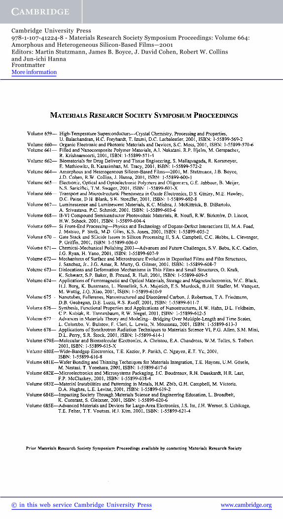
MATERIALS RESEARCH SOCIETY SYMPOSIUM PROCEEDINGS
Volume 633— Nanotubes and Related Materials, A.M. Rao, 2001, ISBN: 1-55899-543-9Volume 634— Structure and Mechanical Properties of Nanophase Materials—Theory and Computer Simulations
vs. Experiment, D. Farkas, H. Kung, M. Mayo, H. Van Swygenhoven, J. Weertman, 2001,ISBN: 1-55899-544-7
Volume 635— Anisotropic Nanoparticles—Synthesis, Characterization and Applications, S.J. Stranick, P. Searson,L.A. Lyon, CD. Keating, 2001, ISBN: 1-55899-545-5
Volume 636— Nonlithographic and Lithographic Methods of Nanofabrication—From Ultralarge-Scale Integrationto Photonics to Molecular Electronics, L. Merhari, J.A. Rogers, A. Karim, D.J. Norris, Y. Xia,2001, ISBN: 1-55899-546-3
Volume 637— Microphotonics—Materials, Physics and Applications, K. Wada, P. Wiltzius, T.F. Krauss,K. Asakawa, E.L. Thomas, 2001, ISBN: 1-55899-547-1
Volume 638— Microcrystalline and Nanocrystalline Semiconductors—2000, P.M. Fauchet, J.M. Buriak,L.T. Canham, N. Koshida, B.E. White, Jr., 2001, ISBN: 1-55899-548-X
Volume 639— GaN and Related Alloys—2000, U. Mishra, M.S. Shur, CM. Wetzel, B. Gil, K. Kishino, 2001.ISBN: 1-55899-549-8
Volume 640— Silicon Carbide—Materials, Processing and Devices, A.K. Agarwal, J.A. Cooper, Jr., E. Janzen,M. Skowronski, 2001, ISBN: 1-55899-550-1
Volume 642— Semiconductor Quantum Dots II, R. Leon, S. Fafard, D. Huffaker, R. Notzel, 2001,ISBN: 1-55899-552-8
Volume 643— Quasicyrstals—Preparation, Properties and Applications, E. Belin-Ferre, P.A. Thiel, A-P. Tsai,K. Urban, 2001, ISBN: 1-55899-553-6
Volume 644— Supercooled Liquid, Bulk Glassy and Nanocrystalline States of Alloys, A. Inoue, A.R. Yavari,W.L. Johnson, R.H. Dauskardt, 2001, ISBN: 1-55899-554-4
Volume 645E—Thermal Barrier Coatings—2000, M.A. Antelo, N.P. Padture, B. Pint, S. Sampath, D.J. Wortman,2001, ISBN: 1-55899-555-2
Volume 646— High-Temperature Ordered Intermetallic Alloys IX, J.H. Schneibel, S. Hanada, K.J. Hemker,R.D. Noebe, G. Sauthoff, 2001, ISBN: 1-55899-556-0
Volume 647— Ion Beam Synthesis and Processing of Advanced Materials, D.B. Poker, S.C. Moss, K-H. Heinig,2001, ISBN: 1-55899-557-9
Volume 648— Growth, Evolution and Properties of Surfaces, Thin Films and Self-Organized Structures,S.C Moss, 2001, ISBN: 1-55899-558-7
Volume 649— Fundamentals of Nanoindentation and Nanotribology II, S.P. Baker, R.F. Cook, S.G. Corcoran,N.R. Moody, 2001, ISBN: 1-55899-559-5
Volume 650— Microstructural Processes in Irradiated Materials—2000, G.E. Lucas, L. Snead, M.A. Kirk. Jr.,R.G. Elliman, 2001, ISBN: 1-55899-560-9
Volume 651— Dynamics in Small Confining Systems V, J.M. Drake, J. Klafter, P. Levitz, R.M. Overney,M. Urbakh, 2001, ISBN: 1-55899-561-7
Volume 652— Influences of Interface and Dislocation Behavior on Microstructure Evolution, M. Aindow, M. Asta,M.V. Glazov, D.L. Medlin, A.D. Rollet, M. Zaiser, 2001, ISBN: 1-55899-562-5
Volume 653— Multiscale Modeling of Materials—2000, L.P. Kubin, J.L. Bassani, K. Cho, H. Gao,R.L.B. Selinger, 2001, ISBN: 1-55899-563-3
Volume 654— Structure-Property Relationships of Oxide Surfaces and Interfaces, C.B. Carter, X. Pan, K. Sickafus,H.L. Tuller, T. Wood, 2001, ISBN: 1-55899-564-1
Volume 655— Ferroelectric Thin Films IX, P.C Mclntyre, S.R. Gilbert, M. Miyasaka, R.W. Schwartz,D. Wouters, 2001, ISBN: 1-55899-565-X
Volume 656E—Materials Issues for Tunable RF and Microwave Devices II, S.C Tidrow, W.D. Wilber,S. Streiffer, J. Levy, J. Talvacchio
Volume 657— Materials Science of Microelectromechanical Systems (MEMS) Devices III, M. deBoer, M. Judy,H. Kahn, S.M. Spearing, 2001, ISBN: 1-55899-567-6
Volume 658— Solid-State Chemistry of Inorganic Materials III, M.J. Geselbracht, J.E. Greedan, D.C Johnson,M.A. Subramanian, 2001, ISBN: 1-55899-568-4
www.cambridge.org© in this web service Cambridge University Press
Cambridge University Press978-1-107-41224-8 - Materials Research Society Symposium Proceedings: Volume 664:Amorphous and Heterogeneous Silicon-Based Films—2001Editors: Martin Stutzmann, James B. Boyce, J. David Cohen, Robert W. Collinsand Jun-ichi HannaFrontmatterMore information
MATERIALS RESEARCH SOCIETY SYMPOSIUM PROCEEDINGS
Volume 659— High-Temperature Superconductors—Crystal Chemistry, Processing and Properties,U. Balachandran, H.C. Freyhardt, T. Izumi, D.C. Larbalestier, 2001, ISBN: 1-55899-569-2
Volume 660— Organic Electronic and Photonic Materials and Devices, S.C. Moss, 2001, ISBN: 1-55899-570-6Volume 661— Filled and Nanocomposite Polymer Materials, A.I. Nakatani, R.P. Hjelm, M. Gerspacher,
R. Krishnamoorti, 2001, ISBN: 1-55899-571-4Volume 662— Biomaterials for Drug Delivery and Tissue Engineering, S. Mallapragada, R. Korsmeyer,
E. Mathiowitz, B. Narasimhan, M. Tracy, 2001, ISBN: 1-55899-572-2Volume 664— Amorphous and Heterogeneous Silicon-Based Films—2001, M. Stutzmann, J.B. Boyce,
J.D. Cohen, R.W. Collins, J. Hanna, 2001, ISBN: 1-55899-600-1Volume 665— Electronic, Optical and Optoelectronic Polymers and Oligomers, G.E. Jabbour, B. Meijer,
N.S. Sariciftci, T.M. Swager, 2001, ISBN: 1-55899-601-XVolume 666— Transport and Microstructural Phenomena in Oxide Electronics, D.S. Ginley, M.E. Hawley,
D.C. Paine, D.H. Blank, S.K. Streiffer, 2001, ISBN: 1-55899-602-8Volume 667— Luminescence and Luminescent Materials, K.C. Mishra, J. McKittrick, B. DiBartolo,
A. Srivastava, P.C. Schmidt, 2001, ISBN: 1-55899-603-6Volume 668— II-VI Compound Semiconductor Photovoltaic Materials, R. Noufi, R.W. Birkmire, D. Lincot,
H.W. Schock, 2001, ISBN: 1-55899-604-4Volume 669— Si Front-End Processing—Physics and Technology of Dopant-Defect Interactions III, M.A. Foad,
J. Matsuo, P. Stolk, M.D. Giles, K.S. Jones, 2001, ISBN: 1-55899-605-2Volume 670— Gate Stack and Silicide Issues in Silicon Processing II, S.A. Campbell, C.C. Hobbs, L. Clevenger,
P. Griffin, 2001, ISBN: 1-55899-606-0Volume 671— Chemical-Mechanical Polishing 2001—Advances and Future Challenges, S.V. Babu, K.C. Cadien,
J.G. Ryan, H. Yano, 2001, ISBN: 1-55899-607-9Volume 672— Mechanisms of Surface and Microstrucure Evolution in Deposited Films and Film Structures,
J. Sanchez, Jr., J.G. Amar, R. Murty, G. Gilmer, 2001, ISBN: 1-55899-608-7Volume 673— Dislocations and Deformation Mechanisms in Thin Films and Small Structures, O. Kraft,
K. Schwarz, S.P. Baker, B. Freund, R. Hull, 2001, ISBN: 1-55899-609-5Volume 674— Applications of Ferromagnetic and Optical Materials, Storage and Magnetoelectronics, W.C. Black,
H.J. Borg, K. Bussmann, L. Hesselink, S.A. Majetich, E.S. Murdock, B.J.H. Stadler, M. Vazquez,M. Wuttig, J.Q. Xiao, 2001, ISBN: 1-55899-610-9
Volume 675— Nanotubes, Fullerenes, Nanostructured and Disordered Carbon, J. Robertson, T.A. Friedmann,D.B. Geohegan, D.E. Luzzi, R.S. Ruoff, 2001, ISBN: 1-55899-611-7
Volume 676— Synthesis, Functional Properties and Applications of Nanostructures, H.W. Hahn, D.L. Feldheim,C.P. Kubiak, R. Tannenbaum, R.W. Siegel, 2001, ISBN: 1-55899-612-5
Volume 677— Advances in Materials Theory and Modeling—Bridging Over Multiple-Length and Time Scales,L. Colombo, V. Bulatov, F. Cleri, L. Lewis, N. Mousseau, 2001, ISBN: 1-55899-613-3
Volume 678— Applications of Synchrotron Radiation Techniques to Materials Science VI, P.G. Allen, S.M. Mini,D.L. Perry, S.R. Stock, 2001, ISBN: 1-55899-614-1
Volume 679E—Molecular and Biomolecular Electronics, A. Christou, E.A. Chandross, W.M. Tolles, S. Tolbert.2001, ISBN: 1-55899-615-X
Volume 680E—Wide-Bandgap Electronics, T.E. Kazior, P. Parikh, C. Nguyen, E.T. Yu, 2001,ISBN: 1-55899-616-8
Volume 68IE—Wafer Bonding and Thinning Techniques for Materials Integration, T.E. Haynes, U.M. Gosele,M. Nastasi, T. Yonehara, 2001, ISBN: 1-55899-617-6
Volume 682E—Microelectronics and Microsystems Packaging, J.C. Boudreaux, R.H. Dauskardt, H.R. Last,F.P. McCluskey, 2001, ISBN: 1-55899-618-4
Volume 683E—Material Instabilities and Patterning in Metals, H.M. Zbib, G.H. Campbell, M. Victoria,D.A. Hughes, L.E. Levine, 2001, ISBN: 1-55899-619-2
Volume 684E—Impacting Society Through Materials Science and Engineering Education, L. Broadbelt,K. Constant, S. Gleixner, 2001, ISBN: 1-55899-620-6
Volume 685E—Advanced Materials and Devices for Large-Area Electronics, J.S. Im, J.H. Werner, S. Uchikoga,T.E. Felter, T.T. Voutsas, H.J. Kim, 2001, ISBN: 1-55899-621-4
Prior Materials Research Society Symposium Proceedings available by contacting Materials Research Society
www.cambridge.org© in this web service Cambridge University Press
Cambridge University Press978-1-107-41224-8 - Materials Research Society Symposium Proceedings: Volume 664:Amorphous and Heterogeneous Silicon-Based Films—2001Editors: Martin Stutzmann, James B. Boyce, J. David Cohen, Robert W. Collinsand Jun-ichi HannaFrontmatterMore information