Embed Size (px)
Citation preview

Power and productivityfor a better world™
ABB Switzerland Ltd., Semiconductors has a long history of producing high power rectifier diodes for applications such as high current rectifiers, mainly for aluminium smelting and other metal refining applications, and input rectifiers for large AC-drives. When designing with high power rectifier diodes, there are certain issues to be con-sidered, the most important of these are addressed in this application note.
Application Note 5SYA 2029-03
High power rectifier diodes
2 High power rectifier diodes I Application Note 5SYA 2029-03
Page
1 Rectifier diode product range from ABB 3
2 Data sheet users guide 3
3 Design recommendations 8 3.1 Determining the required Diode voltage rating 8 3.2 Current sharing issues at paralleling of devices 8 3.3 Correct Diode Installation 9 3.4 Over-voltage protection through RC-snubbers 9
4 Additional notes 9 4.1 Further considerations 9 4.2 References 9
Contents
3 High power rectifier diodes I Application Note 5SYA 2029-03
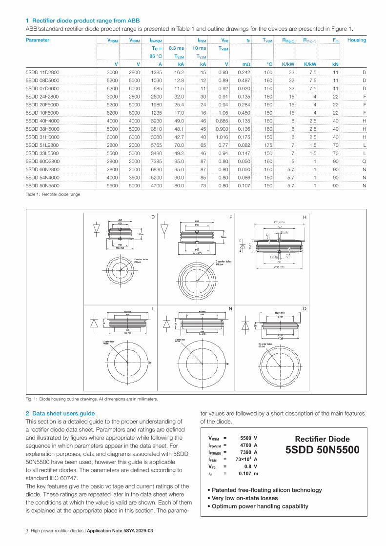
1 Rectifier diode product range from ABBABB’sstandard rectifier diode product range is presented in Table 1 and outline drawings for the devices are presented in Figure 1.
Parameter VRSM VRRM IF(AV)M IFSM VF0 rF TVJM Rth(j-c) Rth(c-h) Fm Housing
Tc = 8.3 ms 10 ms TVJM
85 °C TVJM TVJM
V V A kA kA V m °C K/kW K/kW kN
5SDD 11D2800 3000 2800 1285 16.2 15 0.93 0.242 160 32 7.5 11 D
5SDD 08D5000 5200 5000 1030 12.8 12 0.89 0.487 160 32 7.5 11 D
5SDD 07D6000 6200 6000 685 11.5 11 0.92 0.920 150 32 7.5 11 D
5SDD 24F2800 3000 2800 2600 32.0 30 0.91 0.135 160 15 4 22 F
5SDD 20F5000 5200 5000 1980 25.4 24 0.94 0.284 160 15 4 22 F
5SDD 10F6000 6200 6000 1235 17.0 16 1.05 0.450 150 15 4 22 F
5SDD 40H4000 4000 4000 3930 49.0 46 0.885 0.135 160 8 2.5 40 H
5SDD 38H5000 5000 5000 3810 48.1 45 0.903 0.136 160 8 2.5 40 H
5SDD 31H6000 6000 6000 3080 42.7 40 1.016 0.175 150 8 2.5 40 H
5SDD 51L2800 2800 2000 5765 70.0 65 0.77 0.082 175 7 1.5 70 L
5SDD 33L5500 5500 5000 3480 49.2 46 0.94 0.147 150 7 1.5 70 L
5SDD 60Q2800 2800 2000 7385 95.0 87 0.80 0.050 160 5 1 90 Q
5SDD 60N2800 2800 2000 6830 95.0 87 0.80 0.050 160 5.7 1 90 N
5SDD 54N4000 4000 3600 5200 90.0 85 0.80 0.086 150 5.7 1 90 N
5SDD 50N5500 5500 5000 4700 80.0 73 0.80 0.107 150 5.7 1 90 N
Table 1: Rectifier diode range
Fig. 1: Diode housing outline drawings. All dimensions are in millimeters.
2 Data sheet users guideThis section is a detailed guide to the proper understanding of a rectifier diode data sheet. Parameters and ratings are defined and illustrated by figures where appropriate while following the sequence in which parameters appear in the data sheet. For explanation purposes, data and diagrams associated with 5SDD 50N5500 have been used, however this guide is applicable to all rectifier diodes. The parameters are defined according to standard IEC 60747.The key features give the basic voltage and current ratings of the diode. These ratings are repeated later in the data sheet where the conditions at which the value is valid are shown. Each of them is explained at the appropriate place in this section. The parame-
ter values are followed by a short description of the main features of the diode.
• Patented free-floating silicon technology • Very low on-state losses • Optimum power handling capability
4 High power rectifier diodes I Application Note 5SYA 2029-03
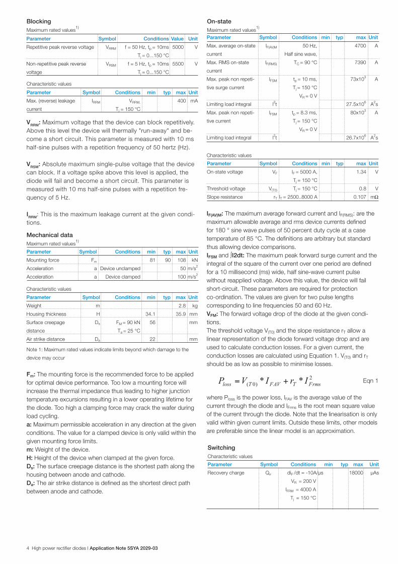
Characteristic values
Parameter Symbol Conditions min typ max Unit
Max. (reverse) leakage IRRM VRRM, 400 mA
current Tj = 150 °C
Note 1: Maximum rated values indicate limits beyond which damage to the
device may occur
Fm: The mounting force is the recommended force to be applied for optimal device performance. Too low a mounting force will increase the thermal impedance thus leading to higher junction temperature excursions resulting in a lower operating lifetime for the diode. Too high a clamping force may crack the wafer during load cycling.a: Maximum permissible acceleration in any direction at the given conditions. The value for a clamped device is only valid within the given mounting force limits.m: Weight of the device.H: Height of the device when clamped at the given force.Ds: The surface creepage distance is the shortest path along the housing between anode and cathode.Da: The air strike distance is defined as the shortest direct path between anode and cathode.
Parameter Symbol Conditions Value Unit
Repetitive peak reverse voltage VRRM f = 50 Hz, tp = 10ms 5000 V
Tj = 0...150 °C
Non-repetitive peak reverse VRSM f = 5 Hz, tp = 10ms 5500 V
voltage Tj = 0...150 °C
BlockingMaximum rated values
1)
Mechanical dataMaximum rated values
1)
Parameter Symbol Conditions min typ max Unit
Mounting force Fm 81 90 108 kN
Acceleration a Device unclamped 50 m/s2
Acceleration a Device clamped 100 m/s2
Characteristic values
Parameter Symbol Conditions min typ max Unit
Weight m 2.8 kg
Housing thickness H 34.1 35.9 mm
Surface creepage Ds FM = 90 kN 56 mm
distance Ta = 25 °C
Air strike distance Da 22 mm
On-stateMaximum rated values
1)
Parameter Symbol Conditions min typ max Unit
Max. average on-state IF(AV)M 50 Hz, 4700 A
current Half sine wave,
Max. RMS on-state IF(RMS) TC = 90 °C 7390 A
current
Max. peak non repeti- IFSM tp = 10 ms, 73x103 A
tive surge current Tj = 150 °C
VR = 0 V
Limiting load integral l2t 27.5x10⁶ A2s
Max. peak non repeti- IFSM tp = 8.3 ms, 80x103 A
tive current Tj = 150 °C
VR = 0 V
Limiting load integral l2t 26.7x10⁶ A2s
Characteristic values
Parameter Symbol Conditions min typ max Unit
On-state voltage VF IF = 5000 A, 1.34 V
Tj = 150 °C
Threshold voltage V(T0) Tj = 150 °C 0.8 V
Slope resistance rT IT = 2500..8000 A 0.107 m
SwitchingCharacteristic values
Parameter Symbol Conditions min typ max Unit
Recovery charge Qrr diF /dt = -10A/µs 18000 µAs
VR = 200 V
IFRM = 4000 A
Tj = 150 °C
VRRM: Maximum voltage that the device can block repetitively. Above this level the device will thermally "run-away" and be-come a short circuit. This parameter is measured with 10 ms half-sine pulses with a repetition frequency of 50 hertz (Hz).
VRSM: Absolute maximum single-pulse voltage that the device can block. If a voltage spike above this level is applied, the diode will fail and become a short circuit. This parameter is measured with 10 ms half-sine pulses with a repetition fre-quency of 5 Hz.
IRRM: This is the maximum leakage current at the given condi-tions.
IF(AV)M: The maximum average forward current and IF(RMS): are the maximum allowable average and rms device currents defined for 180 ° sine wave pulses of 50 percent duty cycle at a case temperature of 85 °C. The definitions are arbitrary but standard thus allowing device comparisons.IFSM and I2dt: The maximum peak forward surge current and the integral of the square of the current over one period are defined for a 10 millisecond (ms) wide, half sine-wave current pulse without reapplied voltage. Above this value, the device will fail short-circuit. These parameters are required for protection co-ordination. The values are given for two pulse lengths corresponding to line frequencies 50 and 60 Hz.VFM: The forward voltage drop of the diode at the given condi-tions.The threshold voltage V(T0) and the slope resistance rT allow a linear representation of the diode forward voltage drop and are used to calculate conduction losses. For a given current, the conduction losses are calculated using Equation 1. V(T0) and rT should be as low as possible to minimise losses. Eqn 1
where Ploss is the power loss, IFAV is the average value of the current through the diode and IFrms is the root mean square value of the current through the diode. Note that the linearisation is only valid within given current limits. Outside these limits, other models are preferable since the linear model is an approximation.

5 High power rectifier diodes I Application Note 5SYA 2029-03
Tvj: The operating junction temperature range gives the limits within which the silicon of the diode should be used. If the limits are exceeded, the ratings for the device are no longer valid and there is a risk of catastrophic failure.Tstg: The temperature interval within which the diode must be stored to ensure that the diode will be operational at a later use.
The thermal resistance junction to case, RthJC, and the thermal resistance case to heat sink, RthCH, are measures of how well the power losses can be transferred to the cooling system. The values are given both for double sided cooling, where the device is clamped between two heat sinks, and single sided cooling, where the device is clamped to only one heat sink. The tempera-ture rise of the «virtual junction» (the silicon wafer inside the diode) in relation to the heat sink is calculated using Equation 2. RthJC and RthCH should be as low as possible since the temperature of the silicon determines the current capability of the diode. Furthermore the temperature excursion of the silicon wafer deter-mines the load-cycling capability and thus the life expectancy of the diode. Eqn 2
where TJH is the temperature difference between the silicon wafer and the heat sink.
The transient thermal impedance emulates the rise of junction temperature versus time when a constant power is dissipated in the junction. This function can either be specified as a curve or as an analytic function with the superposition of four exponential terms. The analytic expression is particularly useful for computer calculations.
ThermalMaximum rated values
1)
Parameter Symbol Conditions min typ max Unit
Operating junction Tvj 0 150 °C
temperature range
Storage temperature Tstg -40 150 °C
range
Characteristic values
Parameter Symbol Conditions min typ max Unit
Thermal resistance Rth(j-c) Double-side 5.7 K/kW
junction to case cooled
Fm = 81...108kN
Rth(j-c)A Anode-side 11.4 K/kW
cooled
Fm = 81...108kN
Rth(j-c)C Cathode-side 11.4 K/kW
cooled
Fm = 81...108kN
Thermal resistance Rth(c-h) Double-side 1 K/kW
case to heatsink cooled
Fm = 81...108kN
Rth(c-h) Single-side 2 K/kW
cooled
Fm = 81...108kN
Fig. 2: Definitions for the turn-off parameters for the Diode
Fig. 1: Transient thermal impedance junction-to-case
Analytical function for transient thermal impedance:
Qrr: Reverse recovery charge. This is the integral over time of the reverse current during commutation at the given conditions starting at the 0-crossing of the reverse current and ending when the reverse current goes back to 0 including the tail-current. See figure 2.
6 High power rectifier diodes I Application Note 5SYA 2029-03
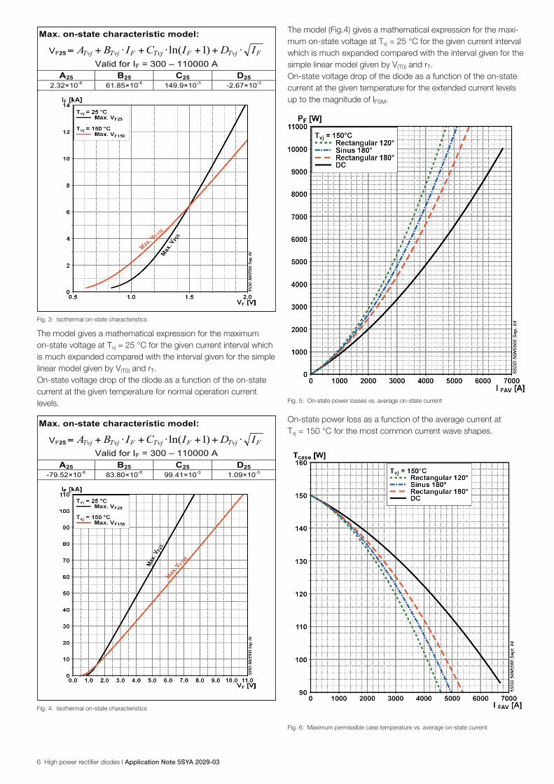
The model gives a mathematical expression for the maximum on-state voltage at Tvj = 25 °C for the given current interval which is much expanded compared with the interval given for the simple linear model given by V(T0) and rT.On-state voltage drop of the diode as a function of the on-state current at the given temperature for normal operation current levels.
Fig. 3: Isothermal on-state characteristics
Fig. 4: Isothermal on-state characteristics
The model (Fig.4) gives a mathematical expression for the maxi-mum on-state voltage at Tvj = 25 °C for the given current interval which is much expanded compared with the interval given for the simple linear model given by V(T0) and rT.On-state voltage drop of the diode as a function of the on-state current at the given temperature for the extended current levels up to the magnitude of IFSM.
Fig. 5: On-state power losses vs. average on-state current
On-state power loss as a function of the average current at Tvj = 150 °C for the most common current wave shapes.
Fig. 6: Maximum permissible case temperature vs. average on-state current
7 High power rectifier diodes I Application Note 5SYA 2029-03
Maximum permissible case temperature as a function of the average current for the most common current wave shapes (Fig.6). Exceeding the average current at a given case tem-perature and current wave shape will lead to overheating of the device.
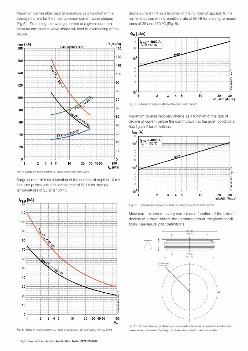
Surge current limit and the surge current integral for half-sine pulses of different pulse widths for starting temperatures of 25 and 150 °C.
Surge current limit as a function of the number of applied 10 ms half-sine pulses with a repetition rate of 50 Ht for starting temperatures of 25 and 150 °C.
Fig. 7: Surge on-state current vs. pulse length, half-sine wave
Fig. 8: Surge on-state current vs. number of pulses, half-sine wave, 10 ms, 50Hz
Fig. 9: Recovery charge vs. decay rate of on-state current
Fig. 10: Peak reverse recovery current vs. decay rate of on-state current
Maximum reverse recovery current as a function of the rate of decline of current before the commutation at the given condi-tions. See figure 2 for definitions.
Maximum reverse recovery charge as a function of the rate of decline of current before the commutation at the given conditions. See figure 2 for definitions.
Surge current limit as a function of the number of applied 10 ms half-sine pulses with a repetition rate of 50 Ht for starting tempera-tures of 25 and 150 °C (Fig. 8).
Fig. 11: Outline drawing; all dimensions are in millimeters and represent nominal values
unless stated otherwise. The height is given in the table for mechanical data.
8 High power rectifier diodes I Application Note 5SYA 2029-03
A list of applicable documents in included at the end of the data sheet.
3 Design recommendations3.1 Determining the required Diode voltage ratingDue to the over-voltage transients that occur on a supply network, especially in an industrial environment, the diode must be carefully chosen to handle most over-voltages without the need of expensive external over-voltage protection. For detailed explanations about the voltage dimensioning and the recom-mended device voltages for a given supply voltage see document 5SYA2051.
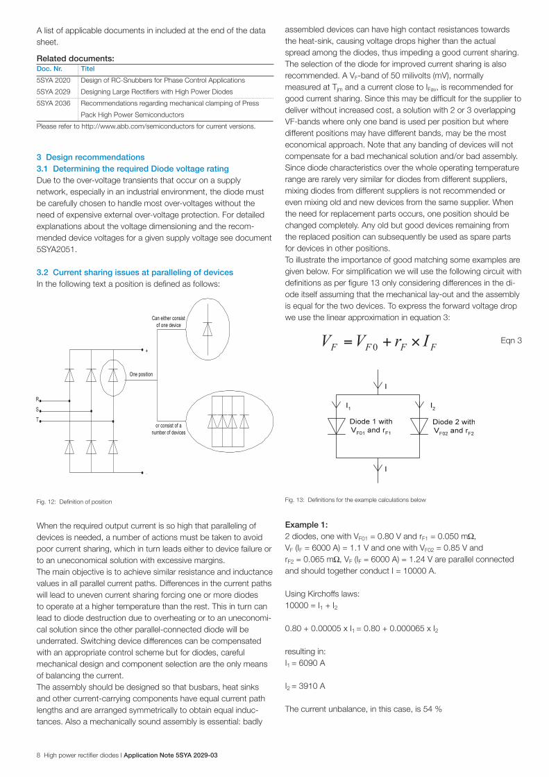
3.2 Current sharing issues at paralleling of devicesIn the following text a position is defined as follows:
When the required output current is so high that paralleling of devices is needed, a number of actions must be taken to avoid poor current sharing, which in turn leads either to device failure or to an uneconomical solution with excessive margins.The main objective is to achieve similar resistance and inductance values in all parallel current paths. Differences in the current paths will lead to uneven current sharing forcing one or more diodes to operate at a higher temperature than the rest. This in turn can lead to diode destruction due to overheating or to an uneconomi-cal solution since the other parallel-connected diode will be underrated. Switching device differences can be compensated with an appropriate control scheme but for diodes, careful mechanical design and component selection are the only means of balancing the current.The assembly should be designed so that busbars, heat sinks and other current-carrying components have equal current path lengths and are arranged symmetrically to obtain equal induc-tances. Also a mechanically sound assembly is essential: badly
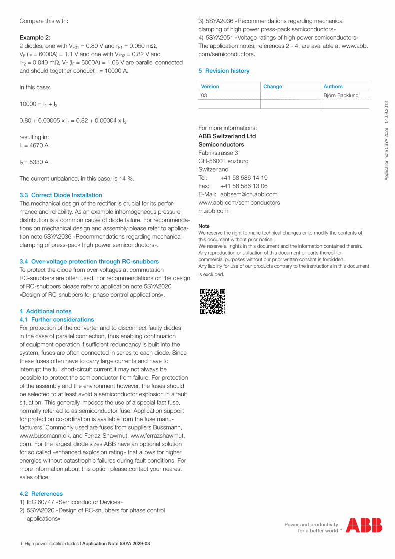
assembled devices can have high contact resistances towards the heat-sink, causing voltage drops higher than the actual spread among the diodes, thus impeding a good current sharing.The selection of the diode for improved current sharing is also recommended. A VF-band of 50 milivolts (mV), normally measured at Tjm and a current close to IFav, is recommended for good current sharing. Since this may be difficult for the supplier to deliver without increased cost, a solution with 2 or 3 overlapping VF-bands where only one band is used per position but where different positions may have different bands, may be the most economical approach. Note that any banding of devices will not compensate for a bad mechanical solution and/or bad assembly.Since diode characteristics over the whole operating temperature range are rarely very similar for diodes from different suppliers, mixing diodes from different suppliers is not recommended or even mixing old and new devices from the same supplier. When the need for replacement parts occurs, one position should be changed completely. Any old but good devices remaining from the replaced position can subsequently be used as spare parts for devices in other positions.To illustrate the importance of good matching some examples are given below. For simplification we will use the following circuit with definitions as per figure 13 only considering differences in the di-ode itself assuming that the mechanical lay-out and the assembly is equal for the two devices. To express the forward voltage drop we use the linear approximation in equation 3: Eqn 3
Example 1:2 diodes, one with VF01 = 0.80 V and rF1 = 0.050 m , VF (IF = 6000 A) = 1.1 V and one with VF02 = 0.85 V and rF2 = 0.065 m , VF (IF = 6000 A) = 1.24 V are parallel connected and should together conduct I = 10000 A.
Using Kirchoffs laws:10000 = I1 + I2
0.80 + 0.00005 x I1 = 0.80 + 0.000065 x I2
resulting in:I1 = 6090 A
I2 = 3910 A
The current unbalance, in this case, is 54 %
Fig. 12: Definition of position
Doc. Nr. Titel
5SYA 2020 Design of RC-Snubbers for Phase Control Applications
5SYA 2029 Designing Large Rectifiers with High Power Diodes
5SYA 2036 Recommendations regarding mechanical clamping of Press
Pack High Power Semiconductors
Please refer to http://www.abb.com/semiconductors for current versions.
Related documents:
Fig. 13: Definitions for the example calculations below
App
licat
ion
note
5S
YA 2
029
04
.09.
2013
For more informations:ABB Switzerland LtdSemiconductorsFabrikstrasse 3CH-5600 LenzburgSwitzerlandTel: +41 58 586 14 19Fax: +41 58 586 13 06E-Mail: [email protected]/semiconductorsm.abb.com
NoteWe reserve the right to make technical changes or to modify the contents of this document without prior notice.We reserve all rights in this document and the information contained therein. Any reproduction or utilisation of this document or parts thereof forcommercial purposes without our prior written consent is forbidden.Any liability for use of our products contrary to the instructions in this document
is excluded.
9 High power rectifier diodes I Application Note 5SYA 2029-03
Compare this with:
Example 2:2 diodes, one with VF01 = 0.80 V and rF1 = 0.050 m , VF (IF = 6000A) = 1.1 V and one with VF02 = 0.82 V and rF2 = 0.040 m , VF (IF = 6000A) = 1.06 V are parallel connected and should together conduct I = 10000 A.
In this case: 10000 = I1 + I2
0.80 + 0.00005 x I1 = 0.82 + 0.00004 x I2
resulting in:I1 = 4670 A
I2 = 5330 A
The current unbalance, in this case, is 14 %.
3.3 Correct Diode InstallationThe mechanical design of the rectifier is crucial for its perfor-mance and reliability. As an example inhomogeneous pressure distribution is a common cause of diode failure. For recommenda-tions on mechanical design and assembly please refer to applica-tion note 5SYA2036 «Recommendations regarding mechanical clamping of press-pack high power semiconductors».
3.4 Over-voltage protection through RC-snubbersTo protect the diode from over-voltages at commutation RC-snubbers are often used. For recommendations on the design of RC-snubbers please refer to application note 5SYA2020 «Design of RC-snubbers for phase control applications».
4 Additional notes4.1 Further considerationsFor protection of the converter and to disconnect faulty diodes in the case of parallel connection, thus enabling continuation of equipment operation if sufficient redundancy is built into the system, fuses are often connected in series to each diode. Since these fuses often have to carry large currents and have to interrupt the full short-circuit current it may not always be possible to protect the semiconductor from failure. For protection of the assembly and the environment however, the fuses should be selected to at least avoid a semiconductor explosion in a fault situation. This generally imposes the use of a special fast fuse, normally referred to as semiconductor fuse. Application support for protection co-ordination is available from the fuse manu-facturers. Commonly used are fuses from suppliers Bussmann, www.bussmann.dk, and Ferraz-Shawmut, www.ferrazshawmut.com. For the largest diode sizes ABB have an optional solution for so called «enhanced explosion rating» that allows for higher energies without catastrophic failures during fault conditions. For more information about this option please contact your nearest sales office.
4.2 References1) IEC 60747 «Semiconductor Devices»2) 5SYA2020 «Design of RC-snubbers for phase control applications»
Version Change Authors
03 Björn Backlund
3) 5SYA2036 «Recommendations regarding mechanical clamping of high power press-pack semiconductors»4) 5SYA2051 «Voltage ratings of high power semiconductors»The application notes, references 2 - 4, are available at www.abb.com/semiconductors.
5 Revision history
Power and productivityfor a better world™