Embed Size (px)
Citation preview
E3065/05/1ELECTRONIC CONTROL DEVICES (PART I)
ELECTRONIC CONTROL DEVICES (PART I)
OBJECTIVES
General objective : To apply the concept of electronic control devices.
Specific objectives : At the end of the unit you should be able to: Identify the power of diodes Define the symbol of diodes List the types of diodes Define the characteristics of diodes Define the application of diodes Draw the construction of diodes Identify the power transistor concept
UNIT 5
E3065/05/2ELECTRONIC CONTROL DEVICES (PART I)
5.1 INTRODUCTION OF POWER DIODE
A diode is a component that allows current to freely flow through it in one direction but essentially stops any current from flowing in the reverse direction. Power diodes can be assumed as ideal switches for most applications but practical diodes differ from the ideal characteristics and have certain limitations. The power diodes are similar to pn-junction signal diodes.
5.2 PRINCIPLE AND CONSTRUCTION OF DIODE
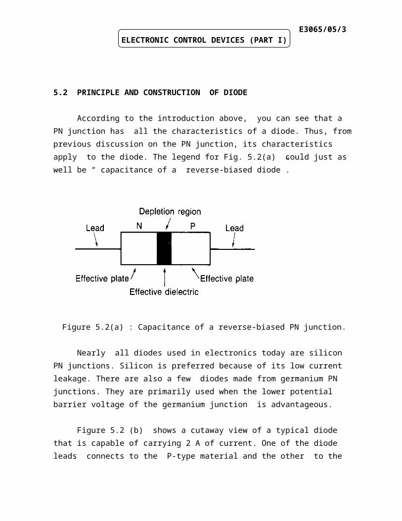
According to the introduction above, you can see that a PN junction has all the characteristics of a diode. Thus, from previous discussion on the PN junction, its characteristics apply to the diode. The legend for Fig. 5.2(a) could just as well be “ capacitance of a reverse-biased diode”.
INPUT
E3065/05/3ELECTRONIC CONTROL DEVICES (PART I)
Figure 5.2(a) : Capacitance of a reverse-biased PN junction.
Nearly all diodes used in electronics today are silicon PN junctions. Silicon is preferred because of its low current leakage. There are also a few diodes made from germanium PN junctions. They are primarily used when the lower potential barrier voltage of the germanium junction is advantageous.
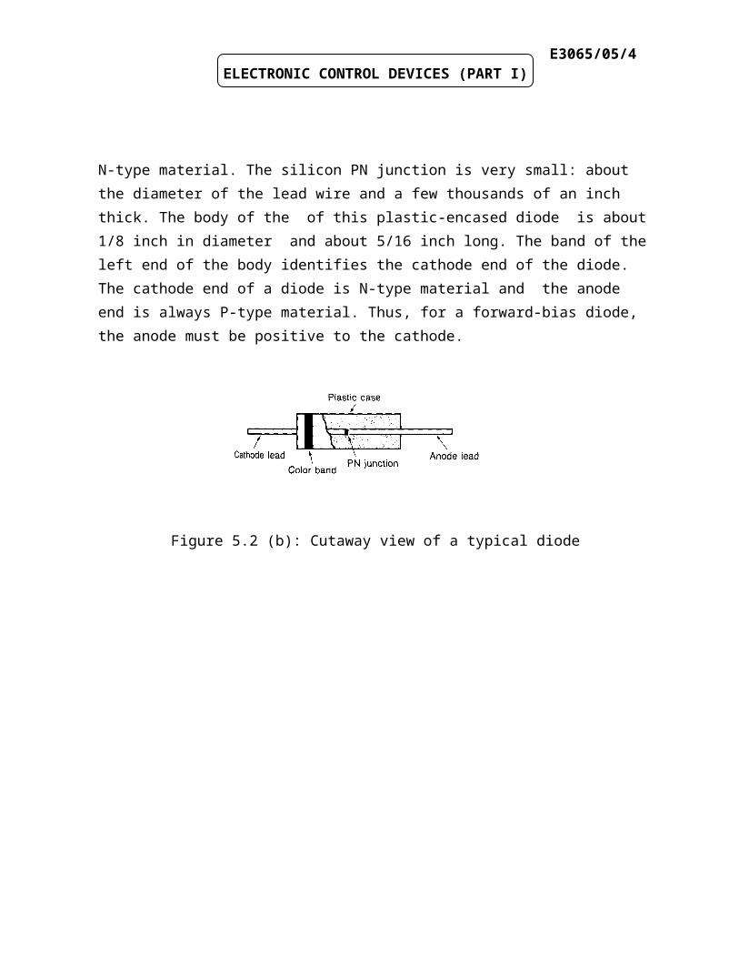
Figure 5.2 (b) shows a cutaway view of a typical diode that is capable of carrying 2 A of current. One of the diode leads connects to the P-type material and the other to the N-type material. The silicon PN junction is very small: about the diameter of the lead wire and a few thousands of an inch thick. The body of the of this plastic-encased diode is about 1/8 inch in diameter and about 5/16 inch long. The band of the left end of the body identifies the cathode end of the diode. The cathode end of a diode is N-type material and the anode end is always P-type material. Thus, for a forward-bias diode, the anode must be positive to the cathode.
Figure 5.2 (b): Cutaway view of a typical diode
E3065/05/4ELECTRONIC CONTROL DEVICES (PART I)
Activity 5A
TEST YOUR UNDERSTANDING BEFORE YOU CONTINUE WITH THE NEXT INPUT…!
5.1. Describe briefly what a diode is.
5.2. Draw a cutaway view of a typical diode.
5.3. Why are silicon diodes preferred over germanium diodes?
Hii !!!!!…..Good Luck and Try your best ….

E3065/05/5ELECTRONIC CONTROL DEVICES (PART I)
Feedback To Activity 5A
5.1. A diode is a component that allows current to freely flow through it in one direction but essentially stops any current from flowing in the reverse direction.
5.2.
Cutaway view of a typical diode
5.3. Silicon diodes are more prevalent because they have less current leakage.

E3065/05/6ELECTRONIC CONTROL DEVICES (PART I)
5.3 SYMBOL OF DIODES.
The schematic symbol for diode is shown in figure 5. 3 (a). The cathode is represented by the vertical straight line and the anode by the triangle. Figure 5.3 (b) and 5.3 (c) illustrate forward-biasing and reverse-biasing respectively.
Figure 5.3 : Schematic symbol for a diode
INPUT
E3065/05/7ELECTRONIC CONTROL DEVICES (PART I)
5.4 TYPES OF POWER DIODES
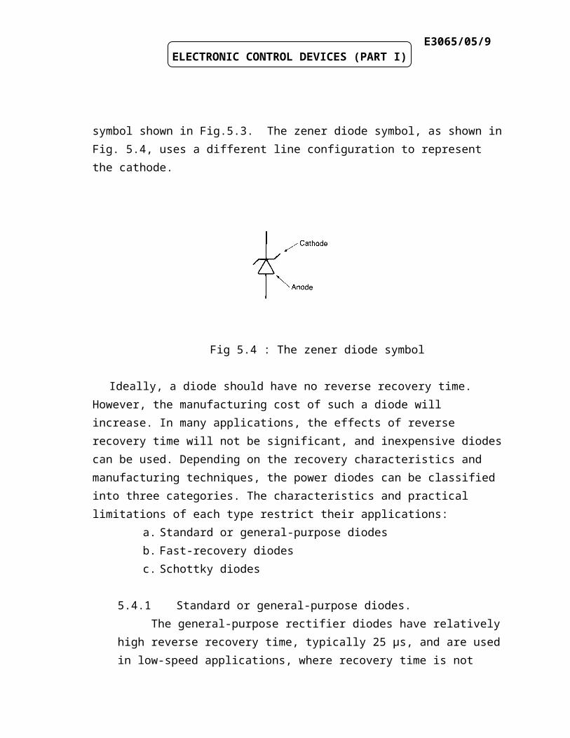
A number of specific types of diodes are manufactured for specific applications in electricity and electronics. Some of the more common types are rectifier diodes, zener diodes, varactor diodes, switching diodes and signal diodes. All of these diodes except the zener diode are represented by the symbol shown in Fig.5.3. The zener diode symbol, as shown in Fig. 5.4, uses a different line configuration to represent the cathode.
Fig 5.4 : The zener diode symbol
Ideally, a diode should have no reverse recovery time. However, the manufacturing cost of such a diode will increase. In many applications, the effects of reverse recovery time will not be significant, and inexpensive diodes can be used. Depending on the recovery characteristics and manufacturing techniques, the power diodes can be classified into three categories. The characteristics and practical limitations of each type restrict their applications:
a. Standard or general-purpose diodesb. Fast-recovery diodes c. Schottky diodes
5.4.1 Standard or general-purpose diodes.The general-purpose rectifier diodes have relatively high reverse recovery
time, typically 25 µs, and are used in low-speed applications, where recovery time is

E3065/05/8ELECTRONIC CONTROL DEVICES (PART I)
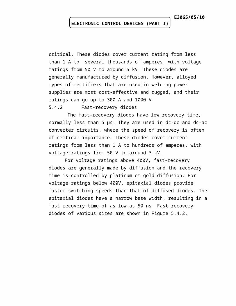
not critical. These diodes cover current rating from less than 1 A to several thousands of amperes, with voltage ratings from 50 V to around 5 kV. These diodes are generally manufactured by diffusion. However, alloyed types of rectifiers that are used in welding power supplies are most cost-effective and rugged, and their ratings can go up to 300 A and 1000 V. 5.4.2 Fast-recovery diodes
The fast-recovery diodes have low recovery time, normally less than 5 µs. They are used in dc-dc and dc-ac converter circuits, where the speed of recovery is often of critical importance. These diodes cover current ratings from less than 1 A to hundreds of amperes, with voltage ratings from 50 V to around 3 kV.
For voltage ratings above 400V, fast-recovery diodes are generally made by diffusion and the recovery time is controlled by platinum or gold diffusion. For voltage ratings below 400V, epitaxial diodes provide faster switching speeds than that of diffused diodes. The epitaxial diodes have a narrow base width, resulting in a fast recovery time of as low as 50 ns. Fast-recovery diodes of various sizes are shown in Figure 5.4.2.
E3065/05/9ELECTRONIC CONTROL DEVICES (PART I)
Figure 5.4.2: Fast-recovery diodes.
5.4.3 Schottky diodes The charge storage problem of a pn-junction can be eliminated (or minimized)
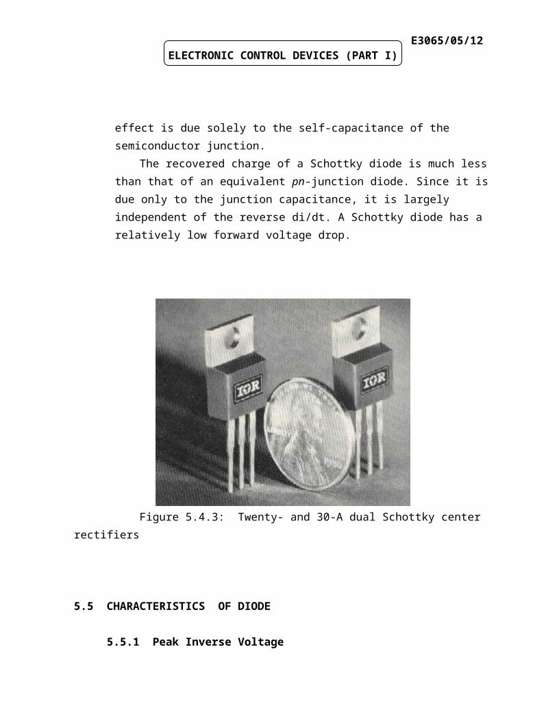
in a Schottky diode. It is accomplished by setting up a “ barrier potential” with a contact between a metal and a semiconductor. A layer of metal is deposited on a thin epitaxial layer of n-type silicon. The potential barrier simulates the behavior of a pn-junction. The rectifying action depends on the majority carriers only, and as a result there are no excess minority carriers to recombine. The recovery effect is due solely to the self-capacitance of the semiconductor junction.
The recovered charge of a Schottky diode is much less than that of an equivalent pn-junction diode. Since it is due only to the junction capacitance, it is largely independent of the reverse di/dt. A Schottky diode has a relatively low forward voltage drop.
Figure 5.4.3: Twenty- and 30-A dual Schottky center rectifiers
E3065/05/10ELECTRONIC CONTROL DEVICES (PART I)
5.5 CHARACTERISTICS OF DIODE
5.5.1 Peak Inverse VoltageA diode can withstand only so much inverse voltage before it breaks down.
The peak inverse voltage (PIV) ranges from 50 V to 4000 V, depending of the construction. If the rated PIV is exceeded, the diode begins to conduct in reverse and in many cases, is immediately destroyed.
5.5.2 Maximum Average CurrentThere is also a limit to the average current a diode can carry. The maximum
current may range from a few hundred milliamperes to over 4000 A, depending of construction and size of the diode. The nominal current rating depends upon the temperature of the diode, which, in turn, depend upon the way it is mounted and how it is cooled.
5.5.3 Maximum Temperature The voltage across a diode times the current it carries is equal to the power lost,
which is entirely converted into heat. The resulting temperature rise of the diode must never exceed the permissible limits, otherwise the diode will be destroyed.
5.6 APPLICATION OF DIODES.
Diodes have many applications, some of which are found again and again, in one form or another, in electronic power circuit. In the sections that follow, we will analyze a few circuit that involve only diodes. They will illustrate the methodology of power circuit analysis while revealing some basic principles common to many industrial applications. Examples of the applications are :
a. battery changer with series resistorb. battery changer with series inductorc. single-phase bridge rectifierd. filter

E3065/05/11ELECTRONIC CONTROL DEVICES (PART I)
e. three-phase, 3-pulse diode rectifierf. three-phase, 6-pulse diode rectifierg. effective line current: fundamental line currenth. distortion power factori. displacement power factorj. harmonic content
Activity 5B
TEST YOUR UNDERSTANDING BEFORE YOU CONTINUE WITH THE NEXT INPUT…!
5.4. Draw a schematic symbol of a diode.
5.5. List FOUR types of diodes.
5.6 List THREE characteristics of a diode.
E3065/05/12ELECTRONIC CONTROL DEVICES (PART I)
Feedback To Activity 5B
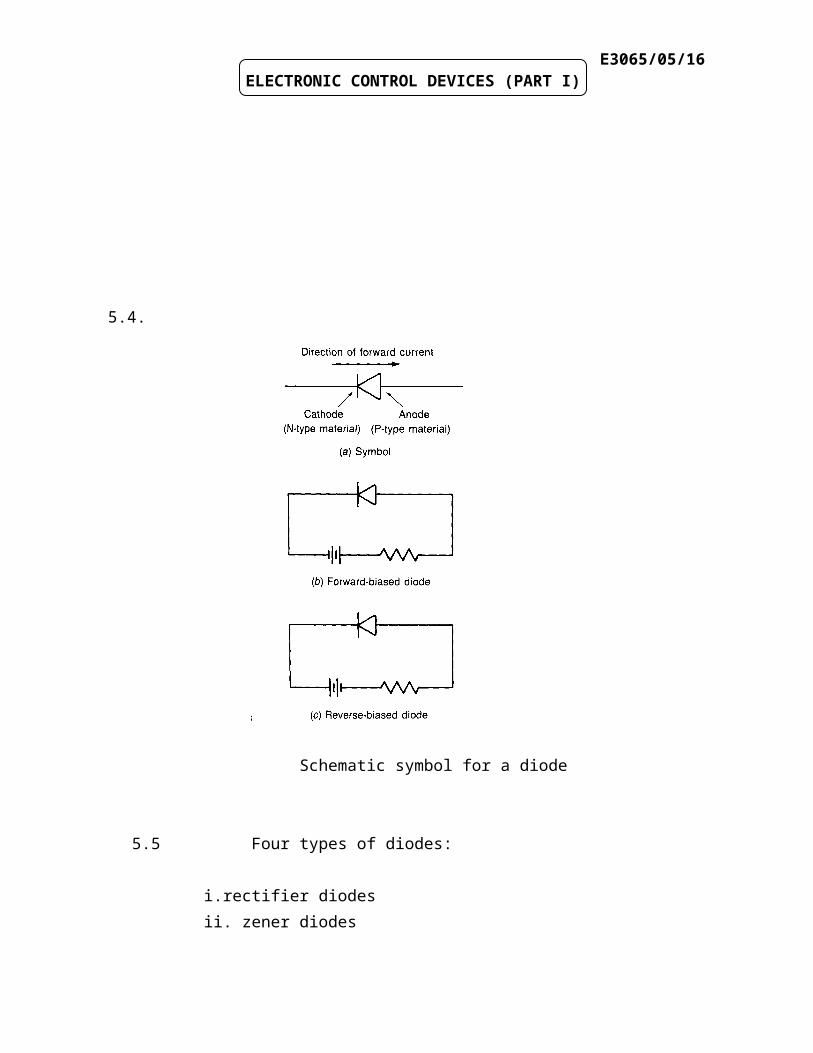
5.4.
E3065/05/13ELECTRONIC CONTROL DEVICES (PART I)
Schematic symbol for a diode
5.5 Four types of diodes:
i.rectifier diodesii. zener diodesiii. varactor diodesiv. switching diodes
5.6 The three characteristics of diode:a.Peak Inverse Voltageb.Maximum Average Currentc.Maximum Temperature
CONGRATULATIONS!!!!…..May success be with you always….
E3065/05/14ELECTRONIC CONTROL DEVICES (PART I)
5.7 POWER TRANSISTORS
Power transistors have controlled turn-on and turn-off characteristics. The transistors, which are used as switching elements, are operated in the saturation region, resulting in a low on-state voltage drop. The switching speed of modern transistors is much higher than that of thyristors and they are extensively employed in dc-dc and dc-ac converters, with inverse parallel-connected diodes to provide bidirectional current flow. However, their voltage and current ratings are lower than those of thyristors and transistors are normally used in low to medium power applications. The power transistors can be classified broadly into four categories:
1. Bipolar junction transistors (BJTs)2. Metal-oxide-semiconductor field-effect transistors (MOSFET)3. Static induction transistors (SITs)4. Insulated-gate bipolar transistors (IGBTs)
BJTs or MOSFETs, SITs or IGBTs, can be assumed as ideal switches to explain the power conversion techniques. A transistor switch is much simpler than a forced-commutated
INPUT
E3065/05/15ELECTRONIC CONTROL DEVICES (PART I)
thyristor switch. However, the choice between a BJT and a MOSFET in the converter circuits is not obvious, but either of them can replace a thyristor, provided that their voltage and current ratings meet the output requirements of the converter. Practical transistors differ from ideal devices. The transistors have certain limitations and are restricted to some applications. The characteristics and ratings of each type should be examined to determine its suitability to a particular application.
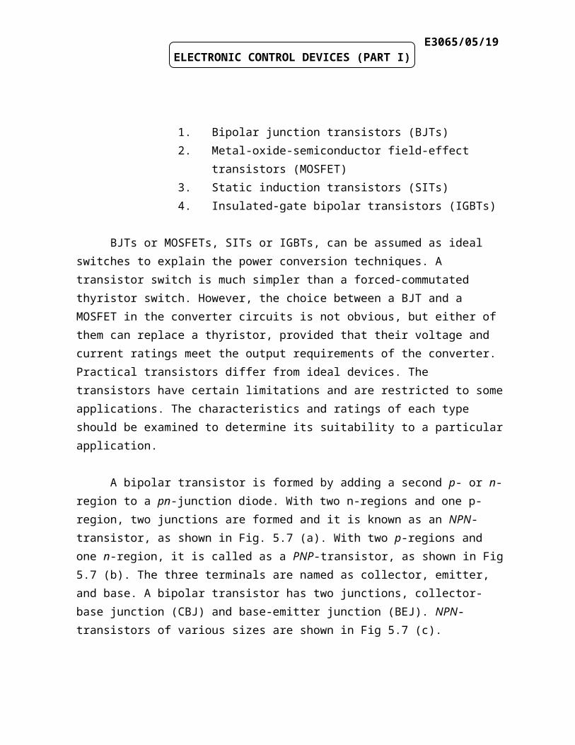
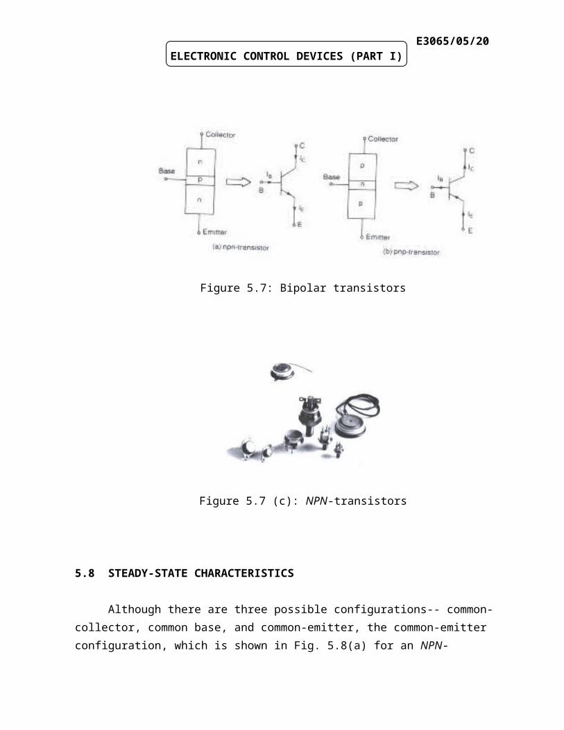
A bipolar transistor is formed by adding a second p- or n-region to a pn-junction diode. With two n-regions and one p-region, two junctions are formed and it is known as an NPN-transistor, as shown in Fig. 5.7 (a). With two p-regions and one n-region, it is called as a PNP-transistor, as shown in Fig 5.7 (b). The three terminals are named as collector, emitter, and base. A bipolar transistor has two junctions, collector-base junction (CBJ) and base-emitter junction (BEJ). NPN-transistors of various sizes are shown in Fig 5.7 (c).
Figure 5.7: Bipolar transistors
E3065/05/16ELECTRONIC CONTROL DEVICES (PART I)
Figure 5.7 (c): NPN-transistors
5.8 STEADY-STATE CHARACTERISTICS
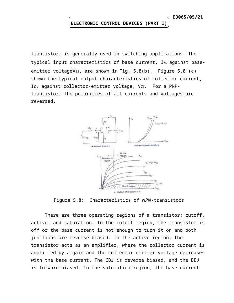
Although there are three possible configurations-- common-collector, common base, and common-emitter, the common-emitter configuration, which is shown in Fig. 5.8(a) for an NPN-transistor, is generally used in switching applications. The typical input characteristics of base current, IB, against base-emitter voltageVBE, are shown in Fig. 5.8(b). Figure 5.8 (c) shown the typical output characteristics of collector current, Ic, against collector-emitter voltage, VcE. For a PNP-transistor, the polarities of all currents and voltages are reversed.
Figure 5.8: Characteristics of NPN-transistors
There are three operating regions of a transistor: cutoff, active, and saturation. In the cutoff region, the transistor is off or the base current is not enough to turn it on and both junctions are reverse biased. In the active region, the transistor acts as an amplifier, where the collector current is amplified by a gain and the collector-emitter voltage decreases with the base current. The CBJ is reverse biased, and the BEJ is forward biased. In the saturation region, the base current is sufficiently high so that the collector-emitter voltage is low, and the
E3065/05/17ELECTRONIC CONTROL DEVICES (PART I)
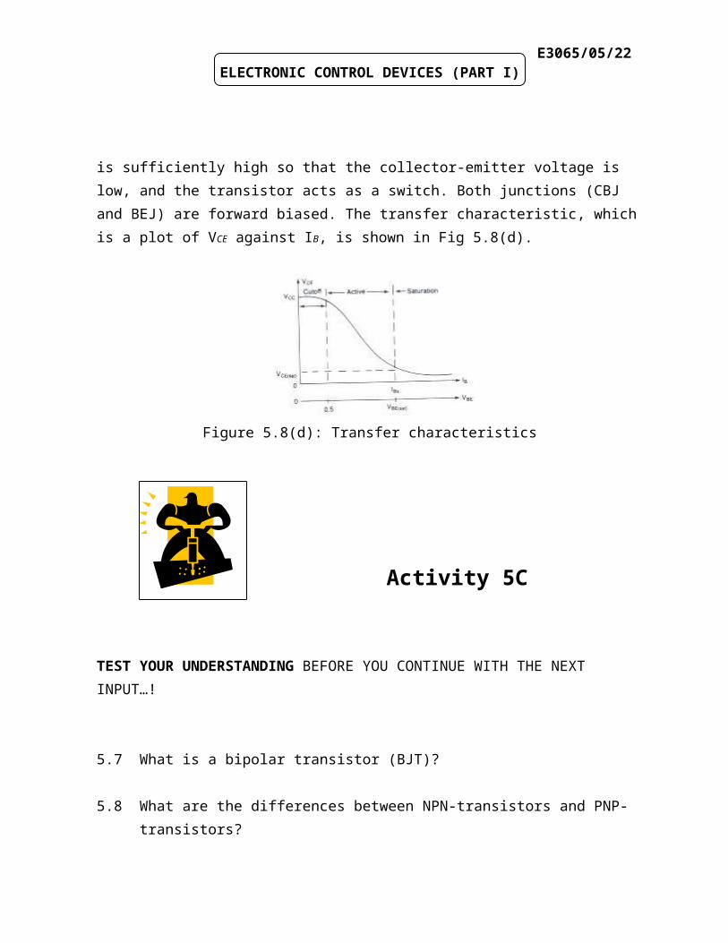
transistor acts as a switch. Both junctions (CBJ and BEJ) are forward biased. The transfer characteristic, which is a plot of VCE against IB, is shown in Fig 5.8(d).
Figure 5.8(d): Transfer characteristics
Activity 5C
TEST YOUR UNDERSTANDING BEFORE YOU CONTINUE WITH THE NEXT INPUT…!
5.7 What is a bipolar transistor (BJT)?
5.8 What are the differences between NPN-transistors and PNP-transistors?
5.9 What are the input characteristics of NPN-transistors?
E3065/05/18ELECTRONIC CONTROL DEVICES (PART I)
Feedback To Activity 5C
5.7 A bipolar transistor is formed by adding as second p- or n-region to a pn-junction diode.
5.8 NPN-transistor with two n-regions and one p-region, two junctions are formed and the PNP-transistor with two p-regions and one n-region.
5.9 The NPN-transistor input characteristics of base current, IB against base-emitter voltage, VBE.
CONGRATULATIONS!!!!…..May success be with you always….
E3065/05/19ELECTRONIC CONTROL DEVICES (PART I)
SELF-ASSESSMENT
You are approaching success. Try all the questions in this self-assessment section and check your answers with those given in the Feedback on Self-Assessment 5 given on the next page. If you face any problems, discuss it with your lecturer. Good luck.
Question 5-1
a. Describe briefly a diode and draw the cutaway view of a typical diode.
b. For reverse-bias a diode, should the anode be negative or positive with respect to the cathode?
c. Why are silicon diodes more prevalent than germanium diodes?
d. Draw a schematic symbol of a diode.
E3065/05/20ELECTRONIC CONTROL DEVICES (PART I)
e. List FOUR types of diodes and shown the zener diode symbol.
f. List THREE types of diodes and briefly describe the characteristics of each type of diode.
g. List FIVE applications of diode.
Question 5-2
a. What are power transistors?
b. What are the output characteristics of NPN-transistors?
c. What are the three regions of operation for BJTs?
Feedback To Self-Assessment
Answer 5-1
(a). A diode is a component that allows current to freely flow through it in one direction but essentially stops any current from flowing in the reverse direction
E3065/05/21ELECTRONIC CONTROL DEVICES (PART I)
Cutaway view of a typical diode
(b). Negative
(c). Silicon diodes are more prevalent because they have less current leakage
(d). The schematic symbol for a diode
E3065/05/22ELECTRONIC CONTROL DEVICES (PART I)
Schematic symbol for a diode
(e). Four types of diodes are:i.rectifier diodesii. zener diodesiii. varactor diodesiv. switching diodes
Zener diode symbol
(f) Three and briefly characteristics of diode.
a. Peak Inverse VoltageA diode can withstand only so much inverse voltage before it breaks down.
The peak inverse voltage (PIV) ranges from 50 V to 4000 V, depends on the construction. If the rated PIV is exceeded, the diode begins to conduct in reverse and in many cases, is immediately destroyed.
b. Maximum Average CurrentThere is also a limit to the average current a diode can carry. The maximum
current may range from a few hundred milliamperes to over 4000 A, depending of on the construction and the size of the diode. The nominal current rating depends upon the temperature of the diode, which, in turn, depend upon the way it is mounted and how it is cooled.

E3065/05/23ELECTRONIC CONTROL DEVICES (PART I)
c. Maximum Temperature The voltage across a diode times the current is carries is equal to a power loss
which is entirely converted into heat. The resulting temperature rise of the diode must never exceed the permissible limits, otherwise the diode will be destroyed.
(g). FIVE applications of a diode:
1. battery changer with series resistor.2. battery changer with series inductor3. single-phase bridge rectifier4. filter5. three-phase, 3-pulse diode rectifier
Answer 5-2
(a) Power transistors have controlled turn-on and turn-off characteristics. The transistors, which are used as switching elements, are operated in the saturation region, resulting in a low on-state voltage drop. The switching speed of modern transistors is much higher than that of thyristors and they are extensively employed in dc-dc and dc-ac converters, with inverse parallel-connected diodes to provide bidirectional current flow.
(b) The output characteristics of NPN-transistors are collector current, Ic, against collector-emitter voltage,VcE.
(c) The three regions of operation for BJTs are cutoff, active, and saturation.
E3065/05/24ELECTRONIC CONTROL DEVICES (PART I)
CONGRATULATIONS!!!!…..May success be with you always….