Embed Size (px)
Citation preview
High Performance Microwave Integrated Filters for 5G Applications
by
Jiacheng Zhang
A thesis submitted to the Faculty of Graduate and Postdoctoral Affairs in partial fulfillment of the requirements for the degree of
Master of Applied Science
in
Electrical and Computer Engineering
Carleton University
Ottawa, Ontario
© 2019
Jiacheng Zhang
ii
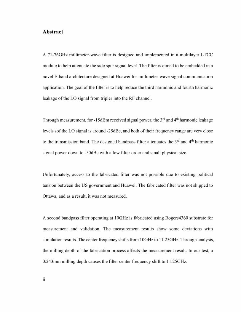
Abstract
A 71-76GHz millimeter-wave filter is designed and implemented in a multilayer LTCC
module to help attenuate the side spur signal level. The filter is aimed to be embedded in a
novel E-band architecture designed at Huawei for millimeter-wave signal communication
application. The goal of the filter is to help reduce the third harmonic and fourth harmonic
leakage of the LO signal from tripler into the RF channel.
Through measurement, for -15dBm received signal power, the 3rd and 4th harmonic leakage
levels sof the LO signal is around -25dBc, and both of their frequency range are very close
to the transmission band. The designed bandpass filter attenuates the 3rd and 4th harmonic
signal power down to -50dBc with a low filter order and small physical size.
Unfortunately, access to the fabricated filter was not possible due to existing political
tension between the US government and Huawei. The fabricated filter was not shipped to
Ottawa, and as a result, it was not measured.
A second bandpass filter operating at 10GHz is fabricated using Rogers4360 substrate for
measurement and validation. The measurement results show some deviations with
simulation results. The center frequency shifts from 10GHz to 11.25GHz. Through analysis,
the milling depth of the fabrication process affects the measurement result. In our test, a
0.243mm milling depth causes the filter center frequency shift to 11.25GHz.

iii
Acknowledgments
First, I’d like to thank professor Rony Amaya and professor Jim Wight. As my supervisor
and co-supervisor, they make a great contribution to my graduate study. I still remember
when I took professor Jim Wight’s PLL class, and I was fascinated by the way he teaches.
So, at that time, I decided to become a research-based student. I must thank professor
Amaya for providing me the funding and the chance to work in Huawei. As a Chinese
citizen, I am so happy and very proud to work in this world-famous Chinese company.
I must thank Morris Repeta and Wenyao Zhai. Morris, as my manager in Huawei, assisted
me in solving many problems from the start of my internship to the end. Wenyao, as my
colleague and a former student of Carleton University, gives me a lot of guidance on filter
design.
I want to thank Kerwin Johnson for reviewing my paper and giving me a lot of guidance.
Besides that, I admire his attitude towards life very much. I am really impressed that he has
never used a mobile phone in his life. It is not easy to live a quiet and undisturbed life today,
but he did it.
There are also many other people I must give my thanks to. I must thank all the millimeter-
wave team member for their kindness help. This made me understand the importance of
the team. Trying to ask for help is sometimes the right choice.
最后我要感谢我的父母, 感谢你们对我的教育,定不负厚望。

iv
Table of Contents
Abstract .............................................................................................................................. ii
Table of Contents ............................................................................................................. iv
List of Tables .................................................................................................................... vi
List of Figures .................................................................................................................. vii
List of Abbreviations and Symbols ................................................................................ xi Chapter 1: Introduction ............................................................................................................. 12
1.1 Motivation and Overview ........................................................................................ 12
1.2 Thesis Contribution .................................................................................................. 15
1.3 Organization ............................................................................................................. 15
Chapter 2: Background knowledge .......................................................................................... 17
2.1 E-band System Architecture..................................................................................... 17
2.2 Spurious signals effect ............................................................................................. 22
2.3 Microwave Component Design ................................................................................ 27
2.4 Resonator design ...................................................................................................... 30
2.5 Summary .................................................................................................................. 33
Chapter 3: Filter design ............................................................................................................ 34
3.1 General description .................................................................................................. 34
3.2 Filter classes ............................................................................................................. 36
3.3 Filter Synthesis ......................................................................................................... 41
3.4 Summary .................................................................................................................. 49
Chapter 4: Filter Implementation ............................................................................................. 51
4.1 Resonator Design ..................................................................................................... 52
4.2 Extract External Quality Factor ................................................................................ 53

v
4.3 Extract Coupling Coefficient ................................................................................... 55
4.4 Filter design and simulation ..................................................................................... 60
4.5 Monte Carlo Analysis .............................................................................................. 63
4.6 Summary .................................................................................................................. 66
Chapter 5: Measurement ........................................................................................................... 67
5.1 Fabrication and measurement .................................................................................. 67
5.2 Analysis of performance .......................................................................................... 70
Chapter 6: Conclusion .............................................................................................................. 75
6.1 Summary .................................................................................................................. 75
6.2 Thesis Contribution .................................................................................................. 75
6.3 Future work .............................................................................................................. 76
Reference ......................................................................................................................... 78
vi
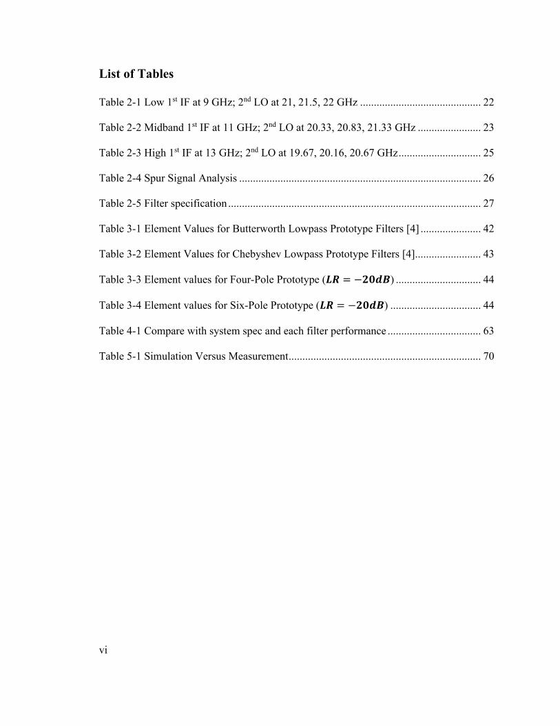
List of Tables
Table 2-1 Low 1st IF at 9 GHz; 2nd LO at 21, 21.5, 22 GHz ............................................ 22
Table 2-2 Midband 1st IF at 11 GHz; 2nd LO at 20.33, 20.83, 21.33 GHz ....................... 23
Table 2-3 High 1st IF at 13 GHz; 2nd LO at 19.67, 20.16, 20.67 GHz .............................. 25
Table 2-4 Spur Signal Analysis ........................................................................................ 26
Table 2-5 Filter specification ............................................................................................ 27
Table 3-1 Element Values for Butterworth Lowpass Prototype Filters [4] ...................... 42
Table 3-2 Element Values for Chebyshev Lowpass Prototype Filters [4] ........................ 43
Table 3-3 Element values for Four-Pole Prototype (𝑳𝑳𝑳𝑳 = −𝟐𝟐𝟐𝟐𝟐𝟐𝟐𝟐) ............................... 44
Table 3-4 Element values for Six-Pole Prototype (𝑳𝑳𝑳𝑳 = −𝟐𝟐𝟐𝟐𝟐𝟐𝟐𝟐) ................................. 44
Table 4-1 Compare with system spec and each filter performance .................................. 63
Table 5-1 Simulation Versus Measurement ...................................................................... 70
vii
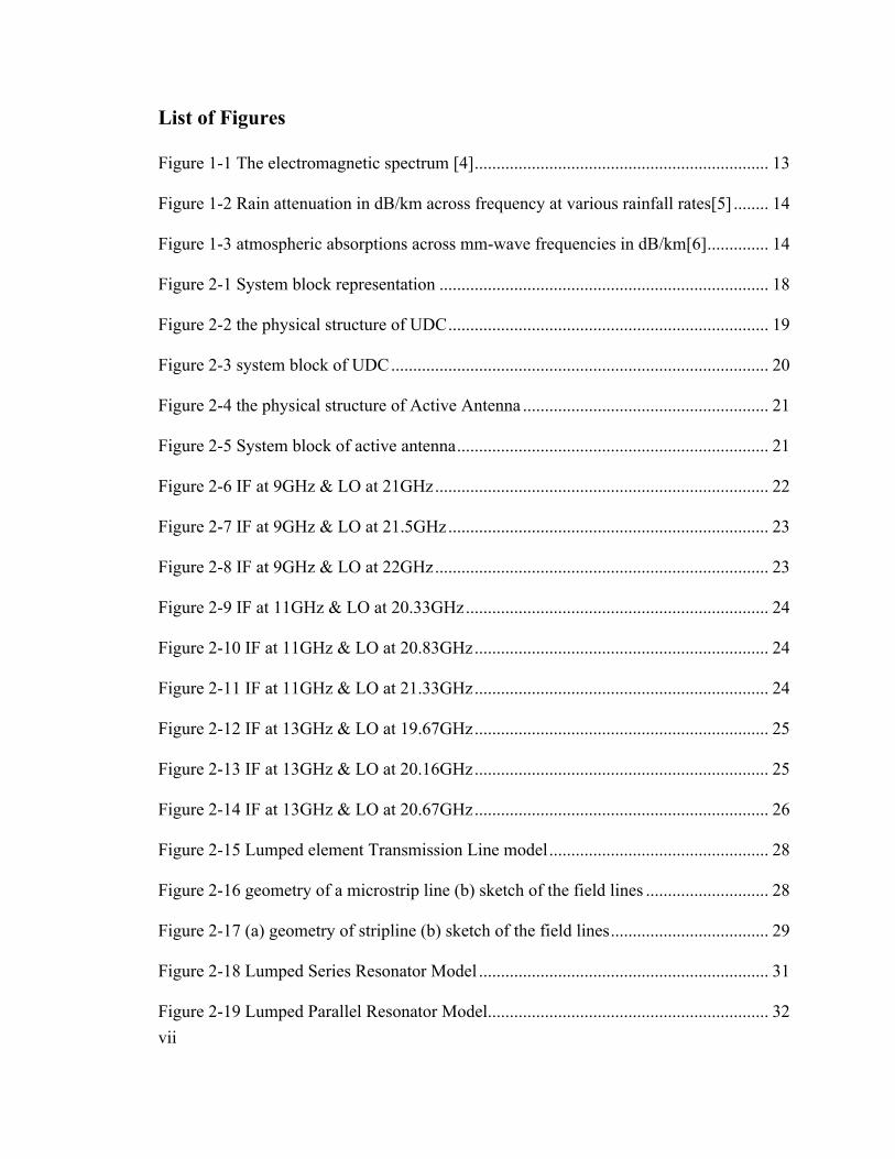
List of Figures
Figure 1-1 The electromagnetic spectrum [4] ................................................................... 13
Figure 1-2 Rain attenuation in dB/km across frequency at various rainfall rates[5] ........ 14
Figure 1-3 atmospheric absorptions across mm-wave frequencies in dB/km[6] .............. 14
Figure 2-1 System block representation ........................................................................... 18
Figure 2-2 the physical structure of UDC ......................................................................... 19
Figure 2-3 system block of UDC ...................................................................................... 20
Figure 2-4 the physical structure of Active Antenna ........................................................ 21
Figure 2-5 System block of active antenna ....................................................................... 21
Figure 2-6 IF at 9GHz & LO at 21GHz ............................................................................ 22
Figure 2-7 IF at 9GHz & LO at 21.5GHz ......................................................................... 23
Figure 2-8 IF at 9GHz & LO at 22GHz ............................................................................ 23
Figure 2-9 IF at 11GHz & LO at 20.33GHz ..................................................................... 24
Figure 2-10 IF at 11GHz & LO at 20.83GHz ................................................................... 24
Figure 2-11 IF at 11GHz & LO at 21.33GHz ................................................................... 24
Figure 2-12 IF at 13GHz & LO at 19.67GHz ................................................................... 25
Figure 2-13 IF at 13GHz & LO at 20.16GHz ................................................................... 25
Figure 2-14 IF at 13GHz & LO at 20.67GHz ................................................................... 26
Figure 2-15 Lumped element Transmission Line model .................................................. 28
Figure 2-16 geometry of a microstrip line (b) sketch of the field lines ............................ 28
Figure 2-17 (a) geometry of stripline (b) sketch of the field lines .................................... 29
Figure 2-18 Lumped Series Resonator Model .................................................................. 31
Figure 2-19 Lumped Parallel Resonator Model ................................................................ 32
viii
Figure 2-20 Transmission Line Terminated at an open-end ............................................. 32
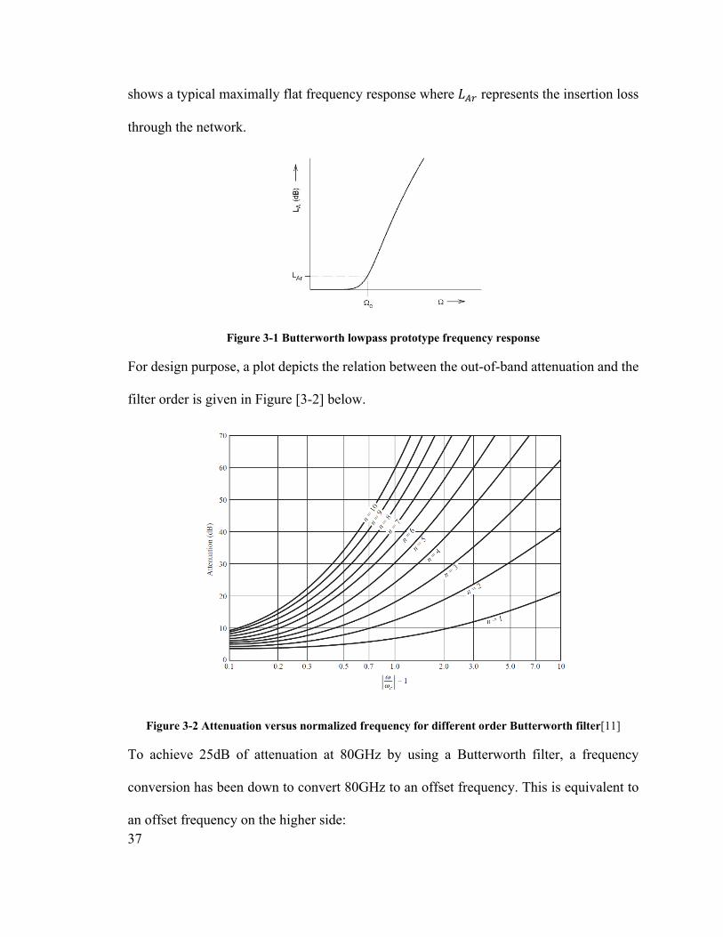
Figure 3-1 Butterworth lowpass prototype frequency response ....................................... 37
Figure 3-2 Attenuation versus normalized frequency for different order Butterworth
filter[11] ............................................................................................................................ 37
Figure 3-3 Chebyshev lowpass prototype frequency response ......................................... 38
Figure 3-4 Attenuation versus normalized frequency for Chebyshev filter[11] ............... 39
Figure 3-5 Elliptic lowpass prototype frequency response ............................................... 40
Figure 3-6 Compare with Chebyshev and the filter with a signal pair of attenuation pole at
finite frequency.[15] ......................................................................................................... 41
Figure 3-7 Lowpass prototype for Butterworth and Chebyshev filter .............................. 42
Figure 3-8 Lowpass prototype for quasi-elliptic filter[13] ............................................... 43
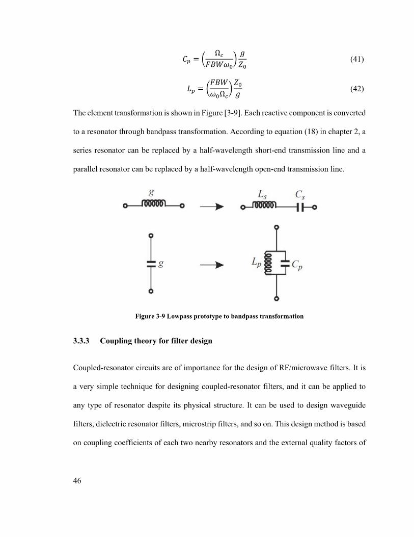
Figure 3-9 Lowpass prototype to bandpass transformation .............................................. 46
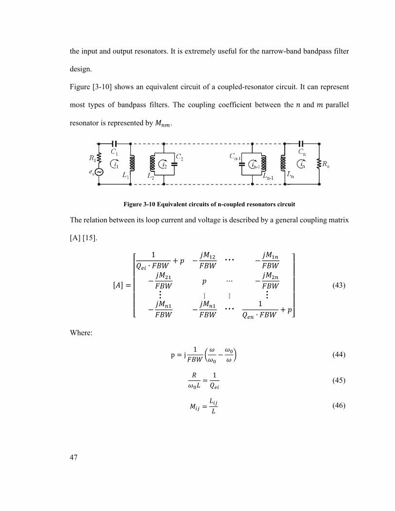
Figure 3-10 Equivalent circuits of n-coupled resonators circuit ....................................... 47
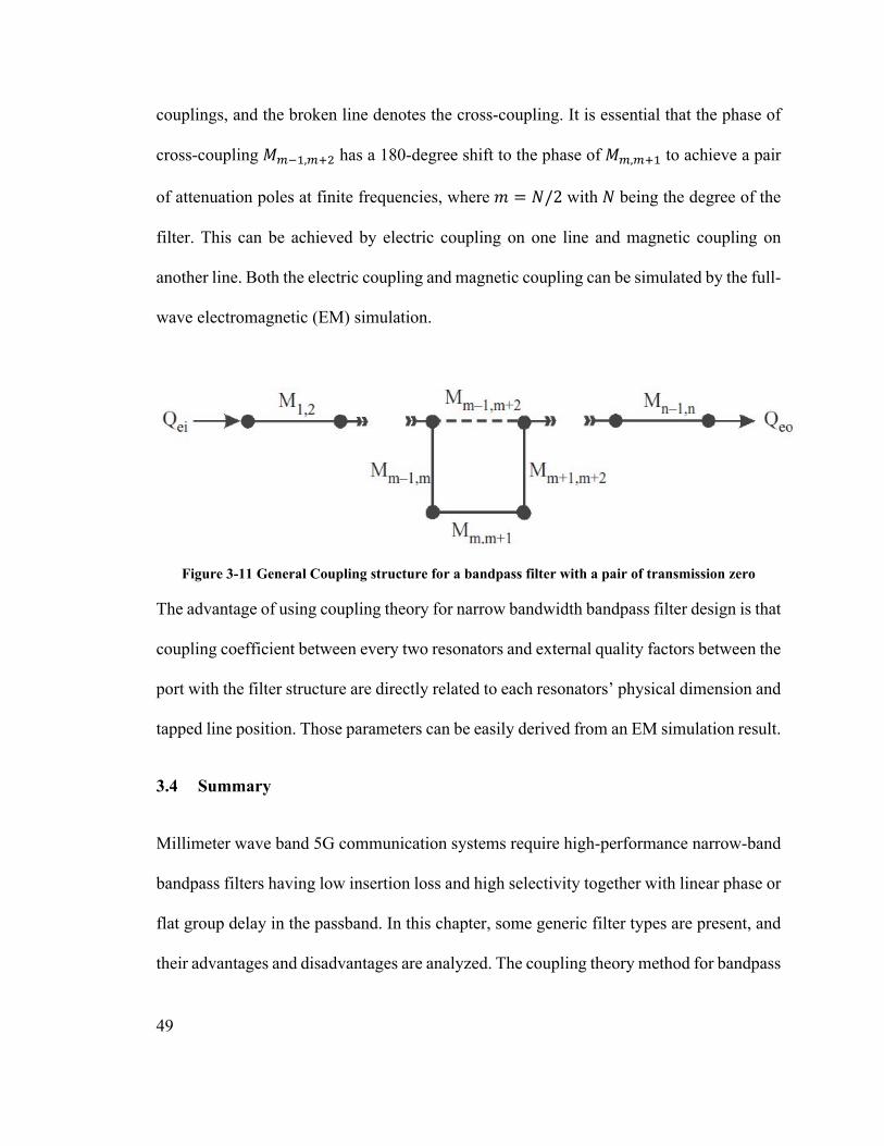
Figure 3-11 General Coupling structure for a bandpass filter with a pair of transmission
zero .................................................................................................................................... 49
Figure 4-1 Four pole filter ................................................................................................. 51
Figure 4-2 six-pole filter structure .................................................................................... 51
Figure 4-3 LTCC substrate structure ................................................................................ 53
Figure 4-4 folded half-wavelength resonator .................................................................... 53
Figure 4-5 tapped-line coupling structure ......................................................................... 54
Figure 4-6 (a) phase response of 𝑺𝑺𝑺𝑺𝑺𝑺 (b) External Q ....................................................... 55
Figure 4-7 Electrical couplings ......................................................................................... 56
Figure 4-8 (a) frequency response; (b) Coupling Coefficient ........................................... 57
ix
Figure 4-9 Magnetic Coupling .......................................................................................... 58
Figure 4-10 (a) Frequency Response of Magnetic Coupling ; (b) Coupling Coefficient
versus distance .................................................................................................................. 59
Figure 4-11 Mixed Coupling ............................................................................................ 60
Figure 4-12 The coupling coefficient of Mix Coupling .................................................... 60
Figure 4-13 Four pole filter............................................................................................... 61
Figure 4-14 Frequency response of Four Pole Filter ........................................................ 61
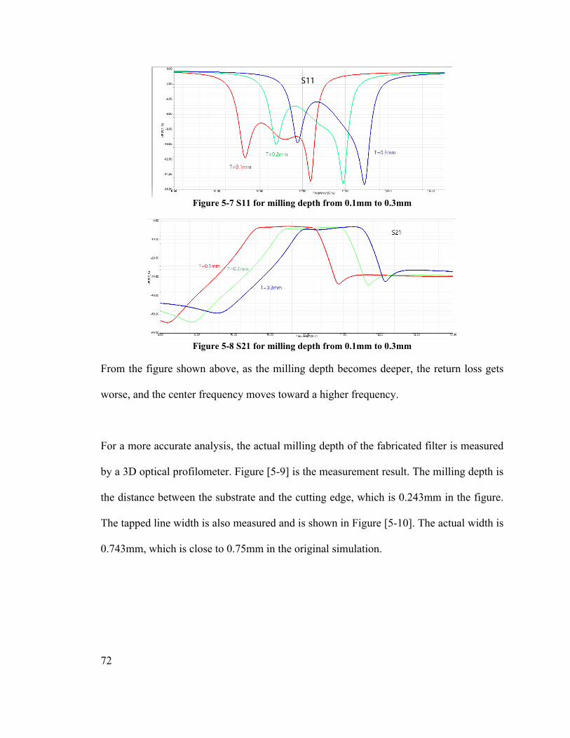
Figure 4-15 six-pole filter structure .................................................................................. 62
Figure 4-16 Frequency response of Six Pole Filter .......................................................... 63
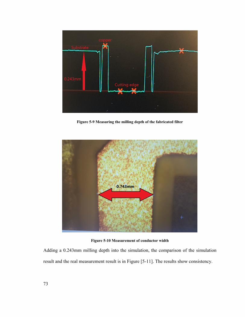
Figure 4-17 Monte Carlo analysis of the fourth-order filter ............................................. 64
Figure 4-18 100 trials of a fourth-order filter Monte Carlo analysis ................................ 65
Figure 4-19 Monte Carlo Analysis for the sixth order filter ............................................. 65
Figure 4-20 100 trials of sixth-order filter Monte Carlo analysis ..................................... 66
Figure 5-1 10GHz Planar Filter ........................................................................................ 67
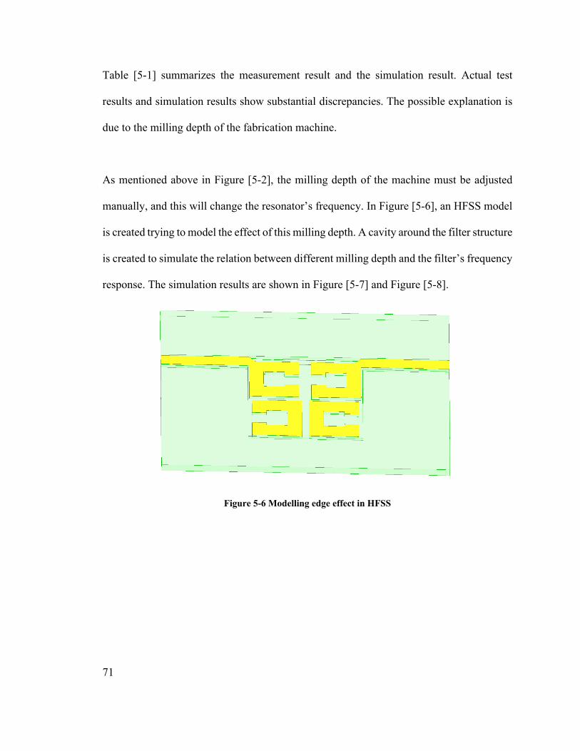
Figure 5-2 LPFK Protomat S100 ...................................................................................... 68
Figure 5-3 Fabricated 10GHz filter ................................................................................... 69
Figure 5-4 Test equipment and calibration module .......................................................... 69
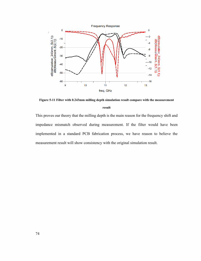
Figure 5-5 Simulation Versus Measurement .................................................................... 70
Figure 5-6 Modelling edge effect in HFSS ....................................................................... 71
Figure 5-7 S11 for milling depth from 0.1mm to 0.3mm ................................................. 72
Figure 5-8 S21 for milling depth from 0.1mm to 0.3mm ................................................. 72
Figure 5-9 Measuring the milling depth of the fabricated filter ....................................... 73
Figure 5-10 Measurement of conductor width.................................................................. 73
x
Figure 5-11 0.243mm milling depth simulation result compare with the measurement result
........................................................................................................................................... 74
Figure 6-1 cascade of two fourth-order filters .................................................................. 77
Figure 6-2 Frequency response of the filter with two pair of transmission zero .............. 77

xi
List of Abbreviations and Symbols
5G The fifth generation of wireless communication
AA Active Antenna
ADS Advanced Design Software
Fn Characteristic Function of filter prototype
FBW Fractional bandwidth
gn Reactive component of a lowpass prototype
kE Electrical Coupling Coefficient
kM Magnetic Coupling Coefficient
LA Insertion Loss of two-port filter
LR Return Loss of two-port filter
LNA Low Noise Amplifier
LTCC Low-Temperature Co-fired Ceramic
PA Power Amplifier
Q Quality Factor of Resonator
RF Radio Frequency
SIW Substrate Integrated Waveguide
UDC Up and Down Converter
Zin Input impedance
Zo Characteristic Impedance
ω0 Center frequency of Resonator
Ωa Transmission zero location
12
Chapter 1: Introduction
1.1 Motivation and Overview
The fifth-generation (5G) wireless standard has already become a reality. Based on recent
VNI report and forecast, in just a decade, the amount of IP data handled by the wireless
network will have increased by well over a factor of 100, from under 3 exabytes in 2010
to over 190 exabytes by 2018, on pace to exceed 500 exabytes by 2020[1]. In addition to
the sheer volume of data, the number of devices and the data rates will continue to grow
exponentially. The number of devices could reach the tens or even hundreds of billions by
the time 5G comes to fruition, due to many new applications beyond personal
communications[2]. Such a rapid increase in mobile data growth and the use of
smartphones are creating unprecedented challenges for wireless service providers to
overcome a global bandwidth shortage.
1.1.1 Millimeter-Wave
The global bandwidth shortage facing wireless carriers has motivated the exploration of
the underutilized millimeter wave frequency spectrum[3] for future broadband cellular
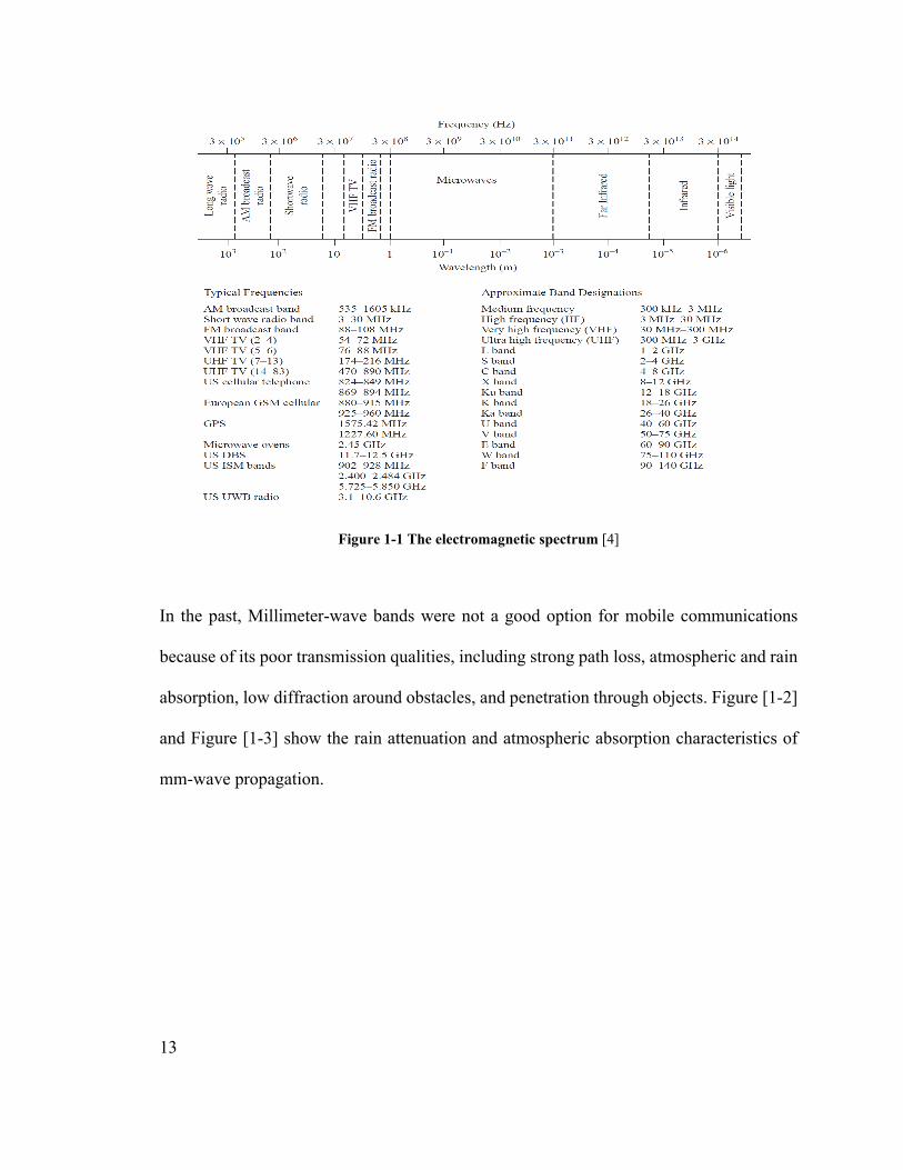
communication networks. Figure [1-1] shows the location of the RF and millimeter-wave
frequency bands in the electromagnetic spectrum and their typical applications. The
millimeter-wave frequency range is between 30GHz to 300GHz, where the wavelength is
from 1-10mm.
13
Figure 1-1 The electromagnetic spectrum [4]
In the past, Millimeter-wave bands were not a good option for mobile communications
because of its poor transmission qualities, including strong path loss, atmospheric and rain
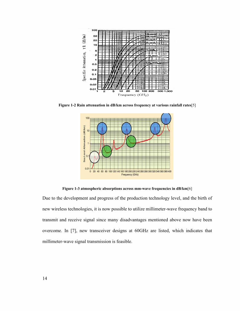
absorption, low diffraction around obstacles, and penetration through objects. Figure [1-2]
and Figure [1-3] show the rain attenuation and atmospheric absorption characteristics of
mm-wave propagation.
14
Figure 1-2 Rain attenuation in dB/km across frequency at various rainfall rates[5]
Figure 1-3 atmospheric absorptions across mm-wave frequencies in dB/km[6]
Due to the development and progress of the production technology level, and the birth of
new wireless technologies, it is now possible to utilize millimeter-wave frequency band to
transmit and receive signal since many disadvantages mentioned above now have been
overcome. In [7], new transceiver designs at 60GHz are listed, which indicates that
millimeter-wave signal transmission is feasible.
15
1.2 Thesis Contribution
Communicating through millimeter-wave frequencies requires a new transceiver
architecture, which includes all circuit components design such as LNA, mixers, filters,
and PA. In this thesis, two different order bandpass filters operating at 71-76GHz are
designed and implemented in an LTCC module, one is forth order, and one is sixth order.
The size of the fourth-order filter is 0.6mm x 0.6mm, and the size of the six-order filter is
1.2mm x 0.6mm. Both filters provide more than 25dB attenuation at 0.1 offset frequency
normalized to the cutoff frequency at 1. The in-band insertion loss is around 5dB, mainly
due to the high conductor loss at 70GHz.
However, the fabricated filters cannot be shipped back to Ottawa for measurement. As a
substitution, another filter fabricated with Rogers 4360G2 materials operating at 10GHz
using the same technology is fabricated and measured for design validation.
1.3 Organization
Chapter 2 presents all the necessary background knowledge. A novel transceiver
architecture transmitting and receiving the EM signal through E-band frequency is first
described on system level. The transceiver structure divides into two parts, the up and down
converter (UDC) and the active antenna (AA). Detail structures of each part are described.
The design equations for microstrip and stripline structure design are given for
transmission line resonator design purpose.
16
Chapter 3 covers the background of the bandpass filter design. Starting from a general
transfer function description, through lowpass prototype synthesis, frequency
transformation, and circuit network equalization, a bandpass filter structure can be
constructed and implemented through coupling theory. Coupling theory is a very useful
filter design method, especially for narrow bandwidth bandpass filter design. It converts
all design parameters into two parameters: the external quality factor and coupling
coefficients. These two parameters are directly related to the physical structure of the filter
and can be simulated through an EM simulator.
Chapter 4 is the detailed procedure for filter design with the assistance of commercial EM
simulator. The design includes how to extract the external quality factor by changing the
tapped line position and how to extract the electric and magnetic coupling coefficient by
changing the gap distance between two resonators. Full-EM simulation software is
necessary for this parameter extraction.
In chapter 5, a planar filter operating at 10 GHz is designed and fabricated for measurement
and validation. Since the processing technology is relatively old, the accuracy of the
produced filter cannot be guaranteed. There is a signification deviation between the test
result and the simulation result. We analyzed the causes of these deviations and made a
conclusion.
17
Chapter 2: Background knowledge
In order to meet the 5G standard and the data transmitting rate requirement, millimeter-
wave communication is now a mainstream research direction. A new type of transceiver
designed by Huawei Technology can transmit a signal at the E-band (71-76GHz) frequency
and use array antenna technology to enhance signal strength and reduce signal interference.
2.1 E-band System Architecture
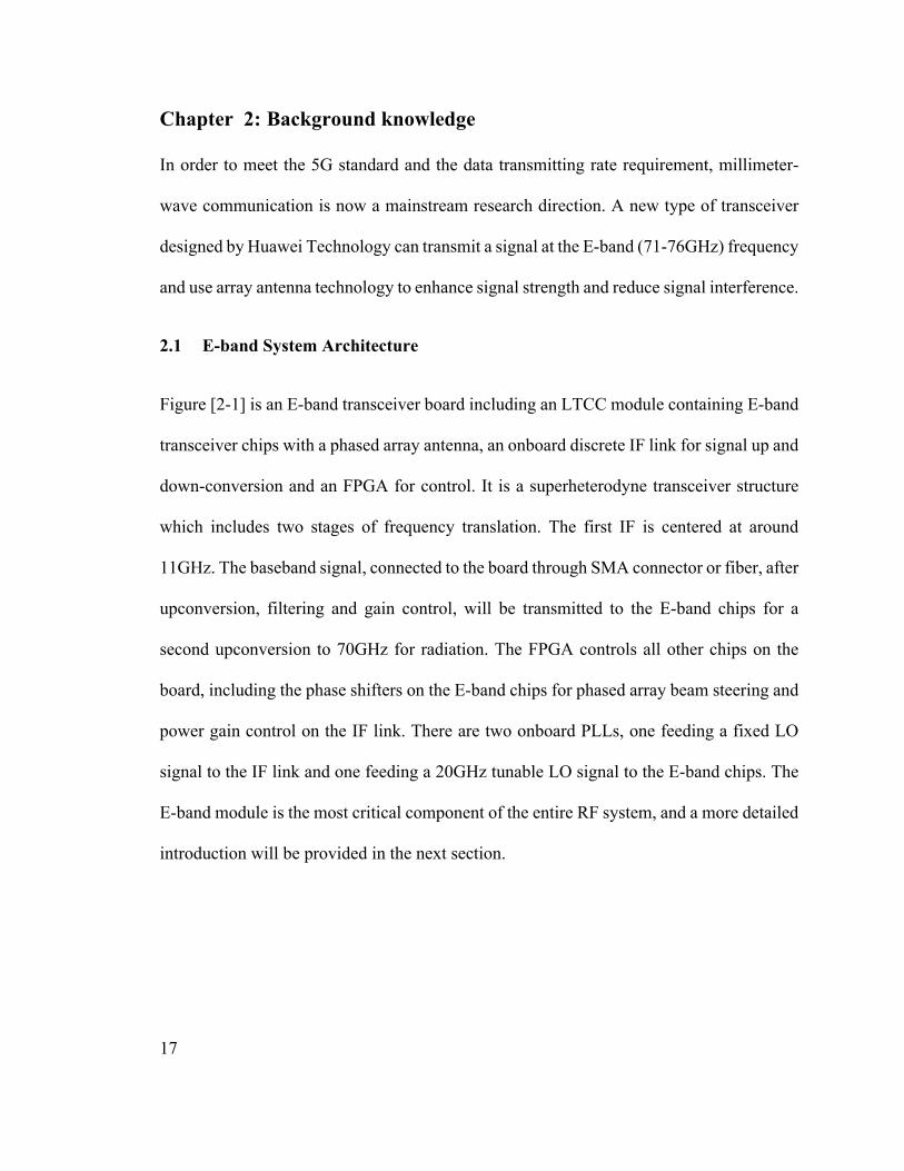
Figure [2-1] is an E-band transceiver board including an LTCC module containing E-band
transceiver chips with a phased array antenna, an onboard discrete IF link for signal up and
down-conversion and an FPGA for control. It is a superheterodyne transceiver structure
which includes two stages of frequency translation. The first IF is centered at around
11GHz. The baseband signal, connected to the board through SMA connector or fiber, after
upconversion, filtering and gain control, will be transmitted to the E-band chips for a
second upconversion to 70GHz for radiation. The FPGA controls all other chips on the
board, including the phase shifters on the E-band chips for phased array beam steering and
power gain control on the IF link. There are two onboard PLLs, one feeding a fixed LO
signal to the IF link and one feeding a 20GHz tunable LO signal to the E-band chips. The
E-band module is the most critical component of the entire RF system, and a more detailed
introduction will be provided in the next section.
18
Figure 2-1 System block representation
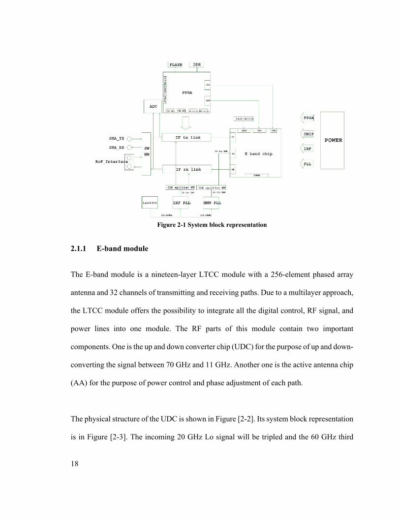
2.1.1 E-band module
The E-band module is a nineteen-layer LTCC module with a 256-element phased array
antenna and 32 channels of transmitting and receiving paths. Due to a multilayer approach,
the LTCC module offers the possibility to integrate all the digital control, RF signal, and
power lines into one module. The RF parts of this module contain two important
components. One is the up and down converter chip (UDC) for the purpose of up and down-
converting the signal between 70 GHz and 11 GHz. Another one is the active antenna chip
(AA) for the purpose of power control and phase adjustment of each path.
The physical structure of the UDC is shown in Figure [2-2]. Its system block representation
is in Figure [2-3]. The incoming 20 GHz Lo signal will be tripled and the 60 GHz third
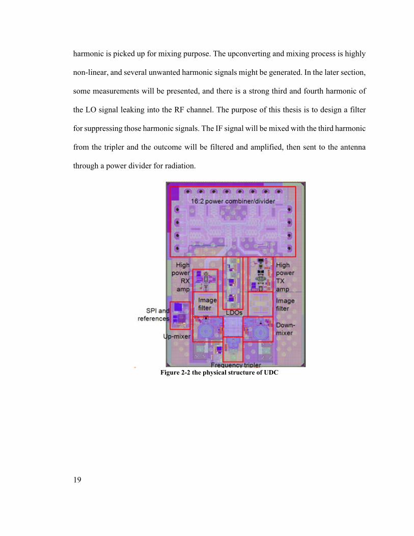
19
harmonic is picked up for mixing purpose. The upconverting and mixing process is highly
non-linear, and several unwanted harmonic signals might be generated. In the later section,
some measurements will be presented, and there is a strong third and fourth harmonic of
the LO signal leaking into the RF channel. The purpose of this thesis is to design a filter
for suppressing those harmonic signals. The IF signal will be mixed with the third harmonic
from the tripler and the outcome will be filtered and amplified, then sent to the antenna
through a power divider for radiation.
Figure 2-2 the physical structure of UDC
20
Figure 2-3 system block of UDC
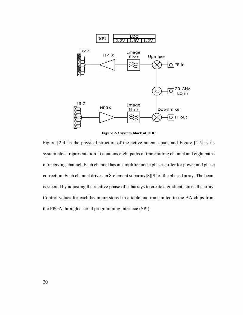
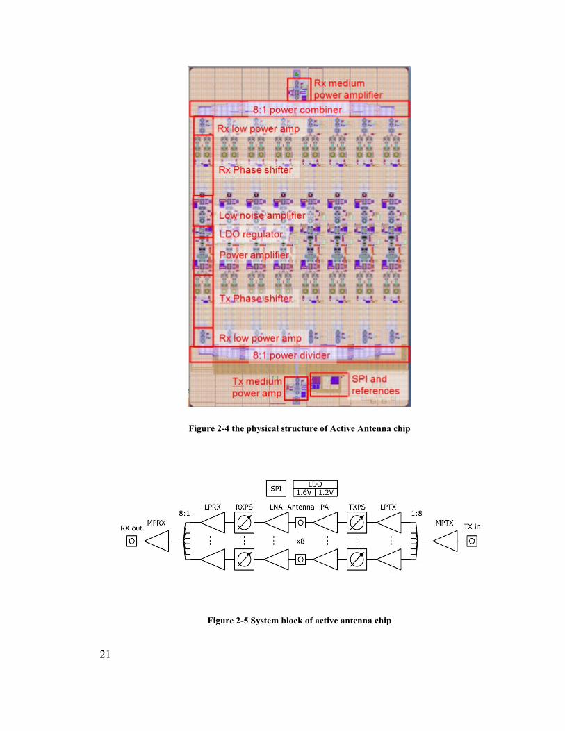
Figure [2-4] is the physical structure of the active antenna part, and Figure [2-5] is its
system block representation. It contains eight paths of transmitting channel and eight paths
of receiving channel. Each channel has an amplifier and a phase shifter for power and phase
correction. Each channel drives an 8-element subarray[8][9] of the phased array. The beam
is steered by adjusting the relative phase of subarrays to create a gradient across the array.
Control values for each beam are stored in a table and transmitted to the AA chips from
the FPGA through a serial programming interface (SPI).
21
Figure 2-4 the physical structure of Active Antenna chip
Figure 2-5 System block of active antenna chip
22
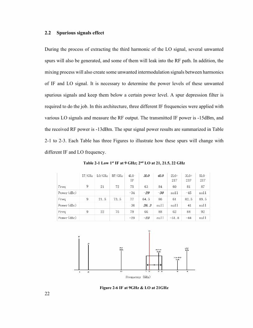
2.2 Spurious signals effect
During the process of extracting the third harmonic of the LO signal, several unwanted
spurs will also be generated, and some of them will leak into the RF path. In addition, the
mixing process will also create some unwanted intermodulation signals between harmonics
of IF and LO signal. It is necessary to determine the power levels of these unwanted
spurious signals and keep them below a certain power level. A spur depression filter is
required to do the job. In this architecture, three different IF frequencies were applied with
various LO signals and measure the RF output. The transmitted IF power is -15dBm, and
the received RF power is -13dBm. The spur signal power results are summarized in Table
2-1 to 2-3. Each Table has three Figures to illustrate how these spurs will change with
different IF and LO frequency.
Table 2-1 Low 1st IF at 9 GHz; 2nd LO at 21, 21.5, 22 GHz
Figure 2-6 IF at 9GHz & LO at 21GHz
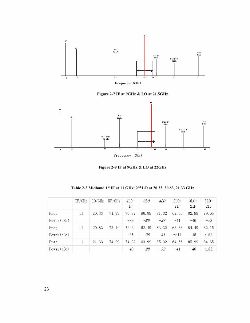
23
Figure 2-7 IF at 9GHz & LO at 21.5GHz
Figure 2-8 IF at 9GHz & LO at 22GHz
Table 2-2 Midband 1st IF at 11 GHz; 2nd LO at 20.33, 20.83, 21.33 GHz
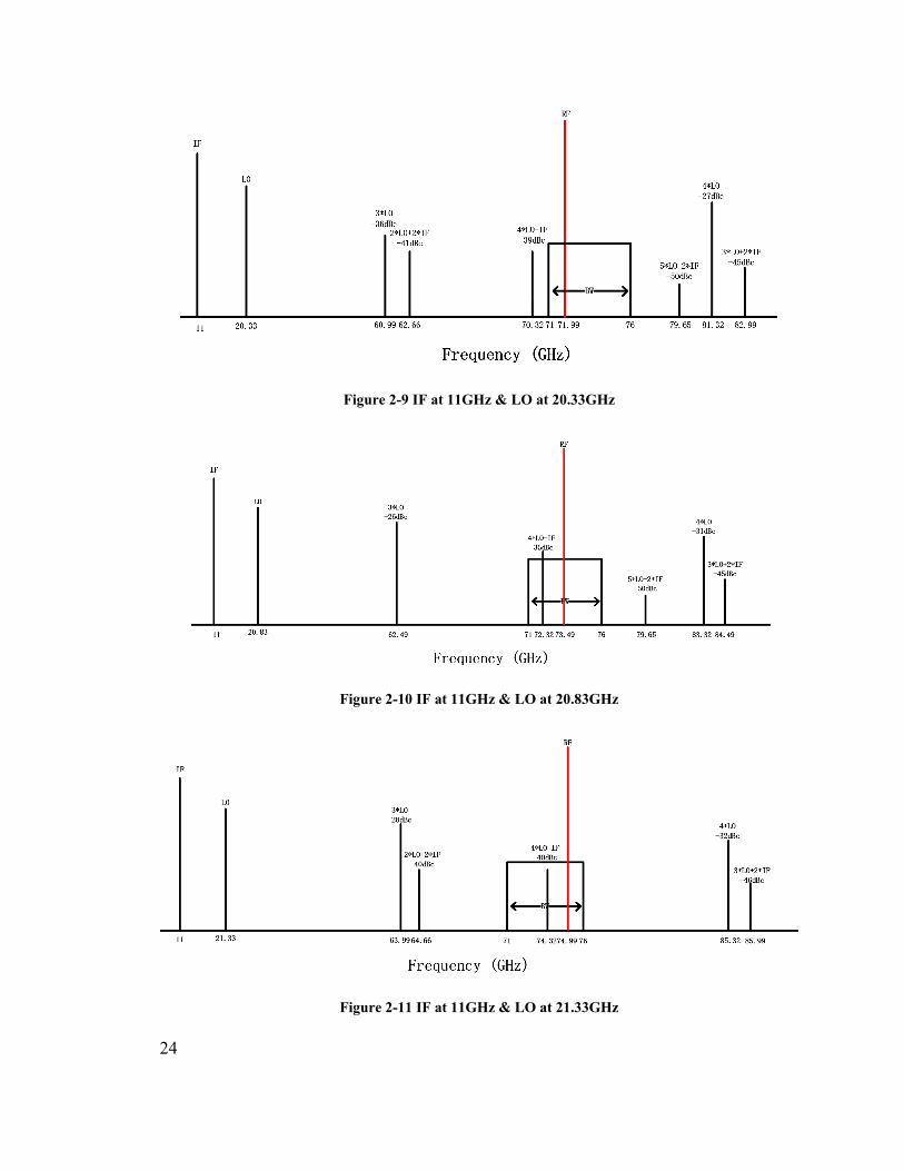
24
Figure 2-9 IF at 11GHz & LO at 20.33GHz
Figure 2-10 IF at 11GHz & LO at 20.83GHz
Figure 2-11 IF at 11GHz & LO at 21.33GHz
25
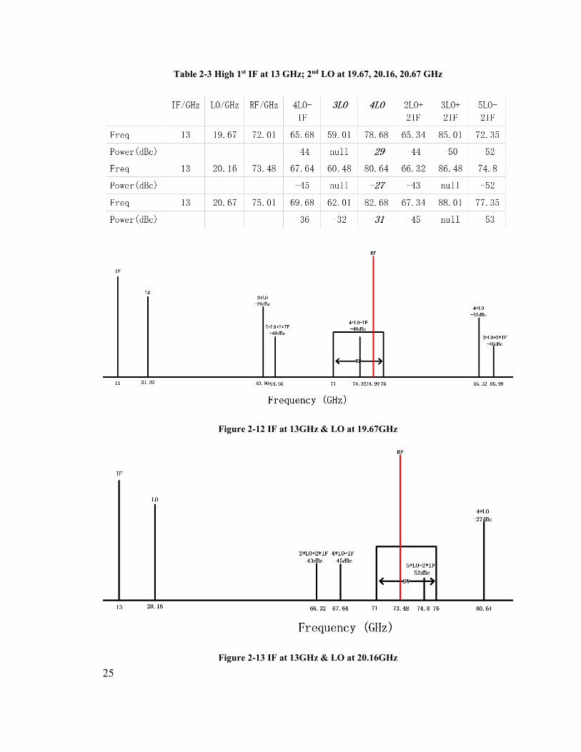
Table 2-3 High 1st IF at 13 GHz; 2nd LO at 19.67, 20.16, 20.67 GHz
Figure 2-12 IF at 13GHz & LO at 19.67GHz
Figure 2-13 IF at 13GHz & LO at 20.16GHz
26
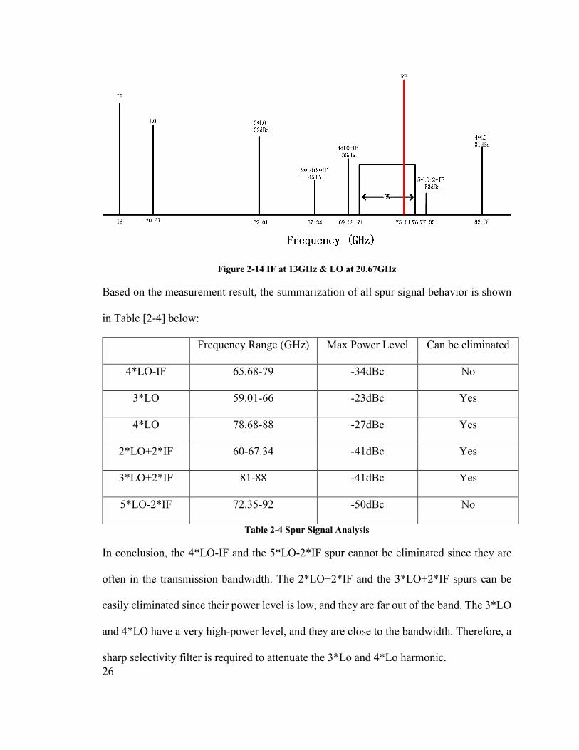
Figure 2-14 IF at 13GHz & LO at 20.67GHz
Based on the measurement result, the summarization of all spur signal behavior is shown
in Table [2-4] below:
Frequency Range (GHz) Max Power Level Can be eliminated
4*LO-IF 65.68-79 -34dBc No
3*LO 59.01-66 -23dBc Yes
4*LO 78.68-88 -27dBc Yes
2*LO+2*IF 60-67.34 -41dBc Yes
3*LO+2*IF 81-88 -41dBc Yes
5*LO-2*IF 72.35-92 -50dBc No
Table 2-4 Spur Signal Analysis
In conclusion, the 4*LO-IF and the 5*LO-2*IF spur cannot be eliminated since they are
often in the transmission bandwidth. The 2*LO+2*IF and the 3*LO+2*IF spurs can be
easily eliminated since their power level is low, and they are far out of the band. The 3*LO
and 4*LO have a very high-power level, and they are close to the bandwidth. Therefore, a
sharp selectivity filter is required to attenuate the 3*Lo and 4*Lo harmonic.
27
Based on these measurement results, we want to attenuate the spur signal power level down
to below -50dBc. Based on this number, a system spec of the filter is given in Table [2-5]
below:
Center frequency 73.45 GHz
Passband 71-76 GHz
FBW 6.8 %
In-band Return Loss <-15 dB
Insertion Loss <5 dB
Out-of-band attenuation -25 dB @68GHz & 80GHz
Table 2-5 Filter specification
A planar filter designed in the LTCC module at this frequency will suffer from a very high
conductor loss and 5dB is a normal value. However, if the filter is designed by a substrate
integrated waveguide (SIW) structure, the insertion loss can be improved down to 2dB or
3dB since conductor losses will be reduced.
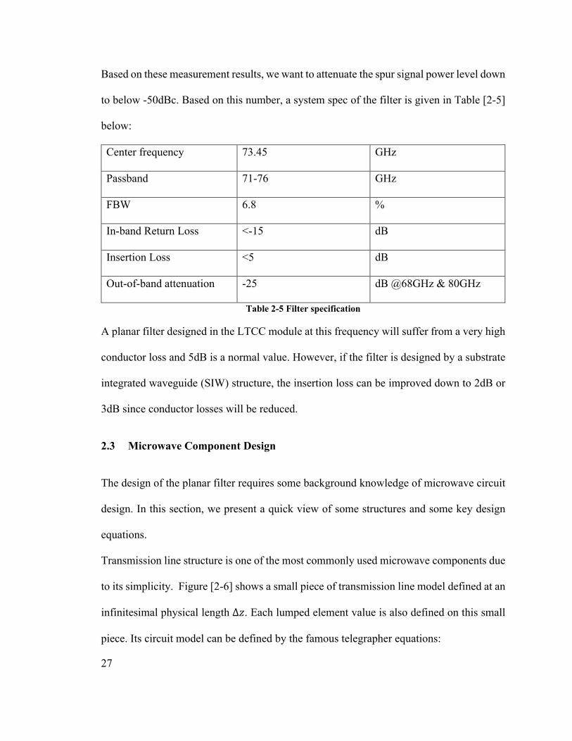
2.3 Microwave Component Design
The design of the planar filter requires some background knowledge of microwave circuit
design. In this section, we present a quick view of some structures and some key design
equations.
Transmission line structure is one of the most commonly used microwave components due
to its simplicity. Figure [2-6] shows a small piece of transmission line model defined at an
infinitesimal physical length ∆𝑧𝑧. Each lumped element value is also defined on this small
piece. Its circuit model can be defined by the famous telegrapher equations:
28
𝜕𝜕𝜕𝜕(𝑧𝑧, 𝑡𝑡)𝜕𝜕𝑧𝑧
= −𝑅𝑅𝑅𝑅(𝑧𝑧, 𝑡𝑡) − 𝐿𝐿𝜕𝜕𝑅𝑅(𝑧𝑧, 𝑡𝑡)𝜕𝜕𝑡𝑡
(1)
𝜕𝜕𝑅𝑅(𝑧𝑧, 𝑡𝑡)𝜕𝜕𝑧𝑧
= −𝐺𝐺𝑅𝑅(𝑧𝑧, 𝑡𝑡) − 𝐶𝐶𝜕𝜕𝑅𝑅(𝑧𝑧, 𝑡𝑡)𝜕𝜕𝑡𝑡
(2)
Figure 2-15 Lumped element Transmission Line model
The important design parameter characteristic impedance 𝑍𝑍𝑜𝑜 is defined as:
𝑍𝑍𝑜𝑜 =𝑅𝑅 + 𝑗𝑗𝑗𝑗𝐿𝐿
𝛾𝛾= �
𝑅𝑅 + 𝑗𝑗𝑗𝑗𝐿𝐿𝐺𝐺 + 𝑗𝑗𝑗𝑗𝐶𝐶
(3)
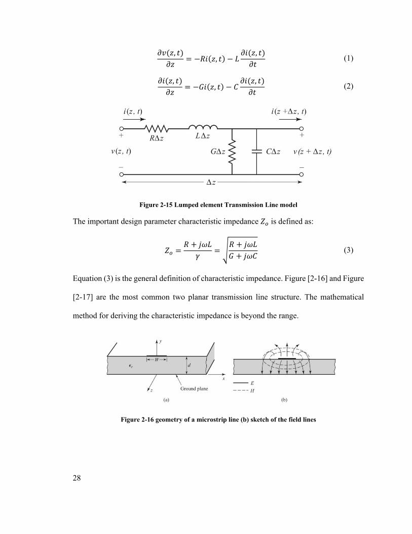
Equation (3) is the general definition of characteristic impedance. Figure [2-16] and Figure
[2-17] are the most common two planar transmission line structure. The mathematical
method for deriving the characteristic impedance is beyond the range.
Figure 2-16 geometry of a microstrip line (b) sketch of the field lines
29
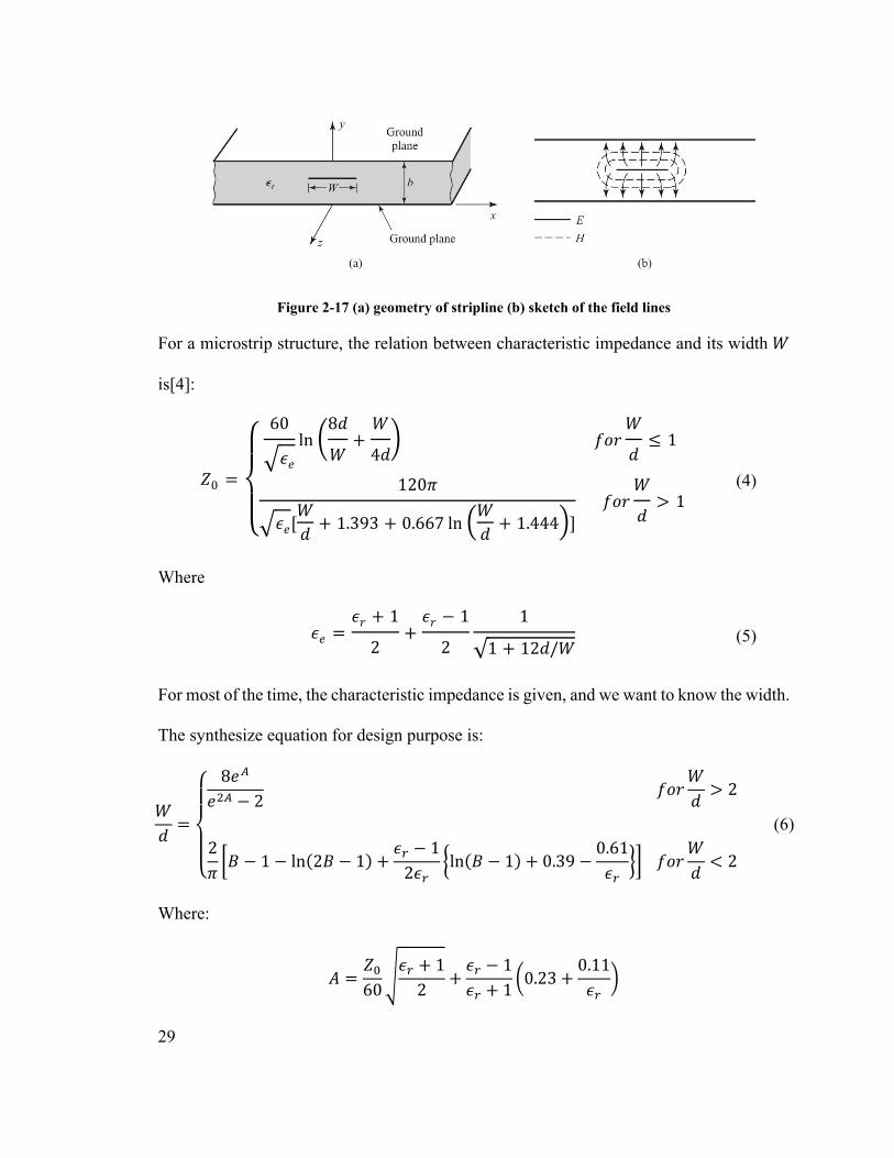
Figure 2-17 (a) geometry of stripline (b) sketch of the field lines
For a microstrip structure, the relation between characteristic impedance and its width 𝑊𝑊
is[4]:
𝑍𝑍0 =
⎩⎪⎨
⎪⎧
60
�𝜖𝜖𝑒𝑒ln �
8𝑑𝑑
𝑊𝑊+𝑊𝑊
4𝑑𝑑� 𝑓𝑓𝑓𝑓𝑓𝑓
𝑊𝑊
𝑑𝑑≤ 1
120𝜋𝜋
�𝜖𝜖𝑒𝑒[𝑊𝑊𝑑𝑑 + 1.393 + 0.667 ln �𝑊𝑊𝑑𝑑 + 1.444�]
𝑓𝑓𝑓𝑓𝑓𝑓𝑊𝑊
𝑑𝑑> 1
(4)
Where
𝜖𝜖𝑒𝑒 =𝜖𝜖𝑓𝑓 + 1
2+𝜖𝜖𝑓𝑓 − 1
2
1
√1 + 12𝑑𝑑/𝑊𝑊 (5)
For most of the time, the characteristic impedance is given, and we want to know the width.
The synthesize equation for design purpose is:
𝑊𝑊𝑑𝑑
=
⎩⎪⎨
⎪⎧ 8𝑒𝑒𝐴𝐴
𝑒𝑒2𝐴𝐴 − 2 𝑓𝑓𝑓𝑓𝑓𝑓
𝑊𝑊𝑑𝑑
> 2
2𝜋𝜋�𝐵𝐵 − 1 − ln(2𝐵𝐵 − 1) +
𝜖𝜖𝑟𝑟 − 12𝜖𝜖𝑟𝑟
�ln(𝐵𝐵 − 1) + 0.39 −0.61𝜖𝜖𝑟𝑟
�� 𝑓𝑓𝑓𝑓𝑓𝑓𝑊𝑊𝑑𝑑
< 2
(6)
Where:
𝐴𝐴 =𝑍𝑍060
�𝜖𝜖𝑟𝑟 + 12
+𝜖𝜖𝑟𝑟 − 1𝜖𝜖𝑟𝑟 + 1 �
0.23 +0.11𝜖𝜖𝑟𝑟
�
30
𝐵𝐵 =377𝜋𝜋
2𝑍𝑍0√𝜖𝜖𝑟𝑟
For a stripline structure in Figure [2-8], the relation between characteristic impedance and
conductor width is[4]:
𝑍𝑍0 =30𝜋𝜋√𝜇𝜇𝑟𝑟
𝑏𝑏𝑊𝑊𝑒𝑒 + 0.441𝑏𝑏
(7)
Where
𝑊𝑊𝑒𝑒
𝑏𝑏=𝑊𝑊
𝑏𝑏− �
0 𝑓𝑓𝑓𝑓𝑓𝑓𝑊𝑊
𝑏𝑏> 0.35
�0.35 −𝑊𝑊
𝑏𝑏�
2
𝑓𝑓𝑓𝑓𝑓𝑓𝑊𝑊
𝑏𝑏< 0.35
The synthesize equation for design purpose is:
𝑊𝑊𝑏𝑏
= �𝑥𝑥 𝑓𝑓𝑓𝑓𝑓𝑓 �𝜖𝜖𝑟𝑟𝑍𝑍0 < 120Ω 0.85 − √0.6 − 𝑥𝑥 𝑓𝑓𝑓𝑓𝑓𝑓 �𝜖𝜖𝑟𝑟𝑍𝑍0 > 120Ω
(8)
Where
𝑥𝑥 =30𝜋𝜋√𝜖𝜖𝑟𝑟𝑍𝑍0
− 0.441
2.4 Resonator design
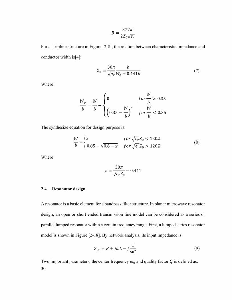
A resonator is a basic element for a bandpass filter structure. In planar microwave resonator
design, an open or short ended transmission line model can be considered as a series or
parallel lumped resonator within a certain frequency range. First, a lumped series resonator
model is shown in Figure [2-18]. By network analysis, its input impedance is:
𝑍𝑍𝑖𝑖𝑖𝑖 = 𝑅𝑅 + 𝑗𝑗𝑗𝑗𝐿𝐿 − 𝑗𝑗1𝑗𝑗𝐶𝐶
(9)
Two important parameters, the center frequency 𝑗𝑗0 and quality factor 𝑄𝑄 is defined as:
31
𝑗𝑗0 =1
√𝐿𝐿𝐶𝐶
(10)
𝑄𝑄 =𝑗𝑗0𝐿𝐿𝑅𝑅
=1
𝑗𝑗0𝑅𝑅𝐶𝐶 (11)
Applying mathematic manipulation, and assuming that ∆𝑗𝑗 is within a small percentage,
the input impedance can be rewritten as:
𝑍𝑍𝑖𝑖𝑖𝑖 = 𝑅𝑅 + 𝑗𝑗2𝑅𝑅𝑄𝑄∆𝑗𝑗𝑗𝑗0
(12)
Figure 2-18 Lumped Series Resonator Model
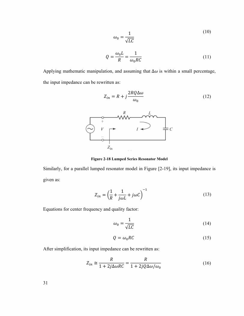
Similarly, for a parallel lumped resonator model in Figure [2-19], its input impedance is
given as:
𝑍𝑍𝑖𝑖𝑖𝑖 = �1𝑅𝑅
+1𝑗𝑗𝑗𝑗𝐿𝐿
+ 𝑗𝑗𝑗𝑗𝐶𝐶�−1
(13)
Equations for center frequency and quality factor:
𝑗𝑗0 =1
√𝐿𝐿𝐶𝐶 (14)
𝑄𝑄 = 𝑗𝑗0𝑅𝑅𝐶𝐶 (15)
After simplification, its input impedance can be rewritten as:
𝑍𝑍𝑖𝑖𝑖𝑖 ≅𝑅𝑅
1 + 2𝑗𝑗∆𝑗𝑗𝑅𝑅𝐶𝐶=
𝑅𝑅1 + 2𝑗𝑗𝑄𝑄∆𝑗𝑗/𝑗𝑗0
(16)
32
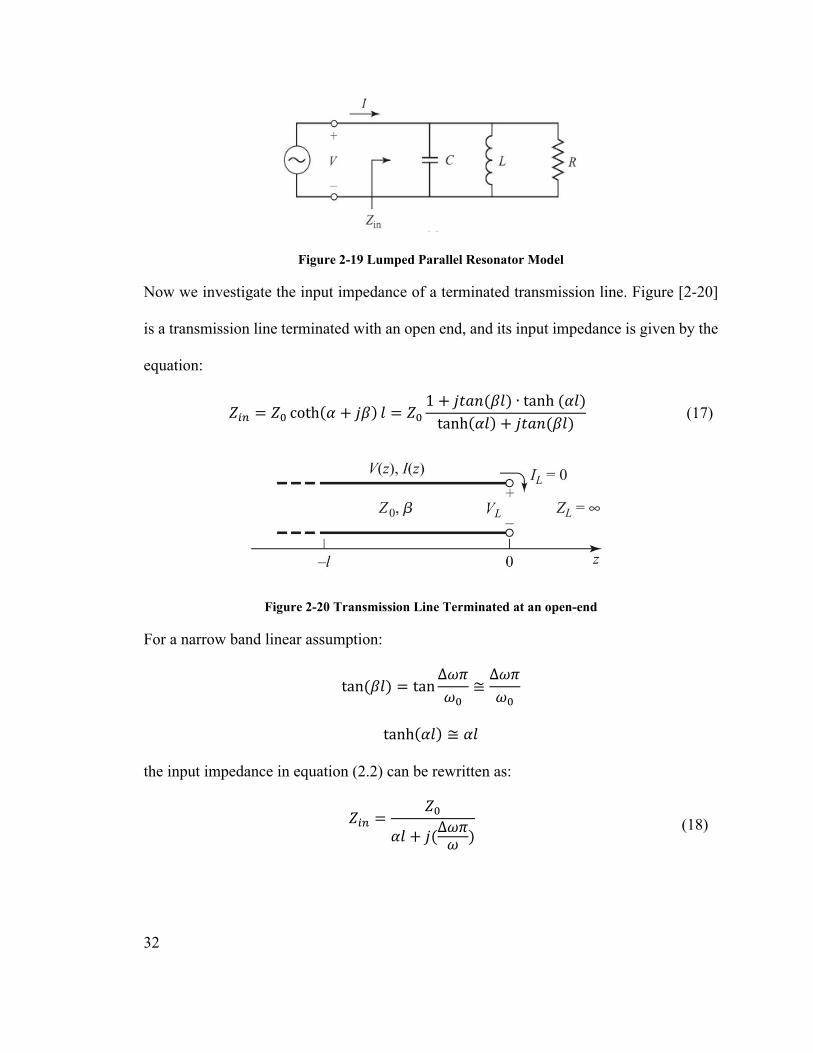
Figure 2-19 Lumped Parallel Resonator Model
Now we investigate the input impedance of a terminated transmission line. Figure [2-20]
is a transmission line terminated with an open end, and its input impedance is given by the
equation:
𝑍𝑍𝑖𝑖𝑖𝑖 = 𝑍𝑍0 coth(𝛼𝛼 + 𝑗𝑗𝑗𝑗) 𝑙𝑙 = 𝑍𝑍01 + 𝑗𝑗𝑡𝑡𝑗𝑗𝑗𝑗(𝑗𝑗𝑙𝑙) ∙ tanh (𝛼𝛼𝑙𝑙)
tanh(𝛼𝛼𝑙𝑙) + 𝑗𝑗𝑡𝑡𝑗𝑗𝑗𝑗(𝑗𝑗𝑙𝑙) (17)
Figure 2-20 Transmission Line Terminated at an open-end
For a narrow band linear assumption:
tan(𝑗𝑗𝑙𝑙) = tan∆𝑗𝑗𝜋𝜋𝑗𝑗0
≅∆𝑗𝑗𝜋𝜋𝑗𝑗0
tanh(𝛼𝛼𝑙𝑙) ≅ 𝛼𝛼𝑙𝑙
the input impedance in equation (2.2) can be rewritten as:
𝑍𝑍𝑖𝑖𝑖𝑖 =𝑍𝑍0
𝛼𝛼𝑙𝑙 + 𝑗𝑗(∆𝑗𝑗𝜋𝜋𝑗𝑗 ) (18)
33
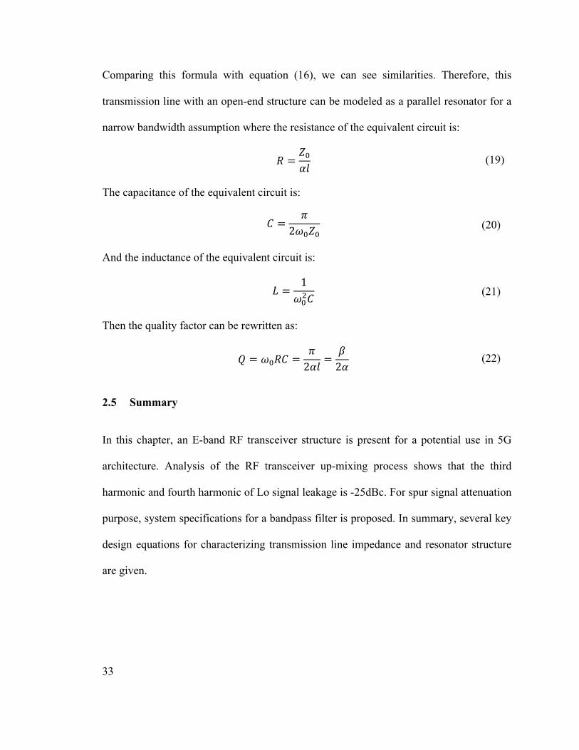
Comparing this formula with equation (16), we can see similarities. Therefore, this
transmission line with an open-end structure can be modeled as a parallel resonator for a
narrow bandwidth assumption where the resistance of the equivalent circuit is:
𝑅𝑅 =𝑍𝑍0𝛼𝛼𝑙𝑙
(19)
The capacitance of the equivalent circuit is:
𝐶𝐶 =𝜋𝜋
2𝑗𝑗0𝑍𝑍0 (20)
And the inductance of the equivalent circuit is:
𝐿𝐿 =1
𝑗𝑗02𝐶𝐶 (21)
Then the quality factor can be rewritten as:
𝑄𝑄 = 𝑗𝑗0𝑅𝑅𝐶𝐶 =𝜋𝜋
2𝛼𝛼𝑙𝑙=
𝑗𝑗2𝛼𝛼
(22)
2.5 Summary
In this chapter, an E-band RF transceiver structure is present for a potential use in 5G
architecture. Analysis of the RF transceiver up-mixing process shows that the third
harmonic and fourth harmonic of Lo signal leakage is -25dBc. For spur signal attenuation
purpose, system specifications for a bandpass filter is proposed. In summary, several key
design equations for characterizing transmission line impedance and resonator structure
are given.
34
Chapter 3: Filter design
3.1 General description
A filter is a two-port network used to control the frequency response at a certain point in
an RF or microwave system by providing transmission at frequencies within the passband
of the filter and attenuation in the stopband of the filter. Typical frequency responses
include low-pass, high-pass, bandpass, and band-reject characteristics. Applications can be
found in virtually any type of RF or microwave communication, radar, or test and
measurement system.
3.1.1 Transfer Functions
An amplitude-squared function for a lossless passive filter network is defined as:
|𝑆𝑆21(𝑗𝑗Ω)|2 =1
1 + 𝜀𝜀2𝐹𝐹𝑖𝑖2(Ω) (23)
Where 𝜀𝜀 is the in-band ripple constant. 𝐹𝐹𝑖𝑖 represents a filtering or characteristic function,
and Ω represents a radian frequency variable of a lowpass prototype filter that has a cut-off
frequency normalized at Ωc = 1
3.1.2 Poles and Zeros
For stability purposes, pole and zeros locations of a transfer function must be checked. For
a linear time-invariant network, equation (23) can be defined as a rational transfer function:
𝑆𝑆21(𝑠𝑠) =𝑁𝑁(𝑠𝑠)𝐷𝐷(𝑠𝑠)
(24)
35
This rational transfer function is defined on the 𝑠𝑠 plane where 𝑠𝑠 = 𝜎𝜎 + 𝑗𝑗Ω. Roots of 𝑁𝑁(𝑠𝑠)
are zeros of the filter and roots of 𝐷𝐷(𝑠𝑠) are poles of the filter. These poles are the natural
frequencies of the filter whose response is described by 𝑆𝑆21(𝑠𝑠). For the filter to be stable,
these natural frequencies must lie in the left half of the p-plane, or on the imaginary axis.
If this were not so, the oscillations would be of exponentially increasing magnitude with
respect to time, a condition that is impossible in a passive network. The zeros of 𝑁𝑁(𝑠𝑠) are
called finite-frequency transmission zeros of the filter.
3.1.3 Filter Specifications
For a given transfer function in Eq. (23), the insertion loss response of the filter can be
computed by:
𝐿𝐿𝐴𝐴(Ω) = 10 log1
|𝑆𝑆21(𝑗𝑗Ω)|2 𝑑𝑑𝐵𝐵 (25)
For a lossless passive two-port network, since there is no power dissipation through the
network, the return loss response of the filter can be computed by:
𝐿𝐿𝑅𝑅(Ω) = 10 log[1 − |𝑆𝑆21(𝑗𝑗Ω)|2]𝑑𝑑𝐵𝐵 (26)
For an ideal filter power response, the in-band insertion loss is 0 dB, and out-of-band return
loss is 0 dB, this means that all in-band signal power is transmitted through the network
and all out-of-band signal is reflected.
The phase Response based on Eq. (24) can be derived as:
∅21(Ω) = 𝐴𝐴𝑓𝑓𝐴𝐴𝑆𝑆21(𝑗𝑗Ω) (27)
The group delay response of this network can then be calculated by:
36
𝜏𝜏𝑑𝑑(Ω) = −𝑑𝑑∅21(Ω)𝑑𝑑Ω
𝑠𝑠 (28)
Phase delay is the time delay for a steady sinusoidal signal; it represents the time it takes
for a carrier signal to travel through the network. The group delay response represents the
true signal delay and needs to be considered since a nonlinear group delay means that an
early transmitting signal might pass through the network after a later transmitting signal.
A flat in-band phase delay is desired for an equal group delay of signals.
3.2 Filter classes
The most common three filter classes are Butterworth, Chebyshev, and Elliptic[11]. We
first introduce each of their transfer function, discuss its advantage and disadvantage. In
the end, another type of filter structure will be presented.
3.2.1 Butterworth, Chebyshev, and Elliptic
Butterworth filter is the simplest filter class. It is quite easy to be designed and implemented.
But it also suffers from poor selectivity, and sometimes even with a higher-order, it can not
meet the required specs. For a Butterworth filter, the characteristic function and the transfer
function are defined as:
𝐹𝐹𝑖𝑖 = Ω2𝑖𝑖
|𝑆𝑆21(𝑗𝑗Ω)|2 =1
1 + Ω2𝑖𝑖
(29)
(30)
where n is the degree or the order of the filter, and the 3dB cut-off frequency is normalized
at Ωc = 1. This structure could provide a maximum in-band flat response. Figure [3-1]
37
shows a typical maximally flat frequency response where 𝐿𝐿𝐴𝐴𝑟𝑟 represents the insertion loss
through the network.
Figure 3-1 Butterworth lowpass prototype frequency response
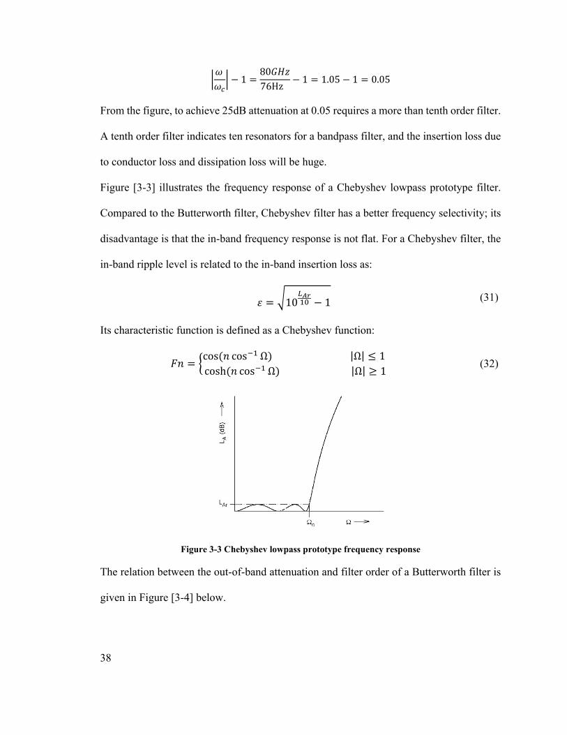
For design purpose, a plot depicts the relation between the out-of-band attenuation and the
filter order is given in Figure [3-2] below.
Figure 3-2 Attenuation versus normalized frequency for different order Butterworth filter[11]
To achieve 25dB of attenuation at 80GHz by using a Butterworth filter, a frequency
conversion has been down to convert 80GHz to an offset frequency. This is equivalent to
an offset frequency on the higher side:
38
�𝑗𝑗
𝑗𝑗𝑐𝑐� − 1 =
80𝐺𝐺𝐺𝐺𝑧𝑧76Hz
− 1 = 1.05 − 1 = 0.05
From the figure, to achieve 25dB attenuation at 0.05 requires a more than tenth order filter.
A tenth order filter indicates ten resonators for a bandpass filter, and the insertion loss due
to conductor loss and dissipation loss will be huge.
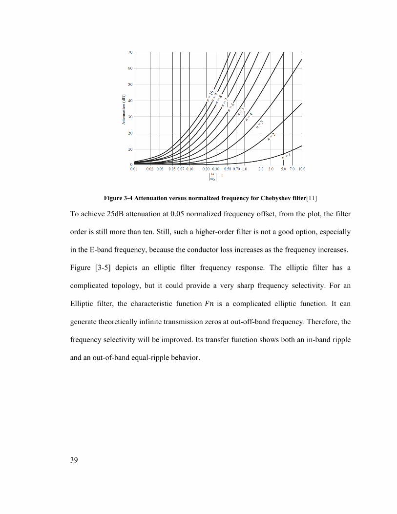
Figure [3-3] illustrates the frequency response of a Chebyshev lowpass prototype filter.
Compared to the Butterworth filter, Chebyshev filter has a better frequency selectivity; its
disadvantage is that the in-band frequency response is not flat. For a Chebyshev filter, the
in-band ripple level is related to the in-band insertion loss as:
𝜀𝜀 = �10𝐿𝐿𝐴𝐴𝐴𝐴10 − 1 (31)
Its characteristic function is defined as a Chebyshev function:
𝐹𝐹𝑗𝑗 = �cos(𝑗𝑗 cos−1 Ω) |Ω| ≤ 1 cosh(𝑗𝑗 cos−1 Ω) |Ω| ≥ 1
(32)
Figure 3-3 Chebyshev lowpass prototype frequency response
The relation between the out-of-band attenuation and filter order of a Butterworth filter is
given in Figure [3-4] below.
39
Figure 3-4 Attenuation versus normalized frequency for Chebyshev filter[11]
To achieve 25dB attenuation at 0.05 normalized frequency offset, from the plot, the filter
order is still more than ten. Still, such a higher-order filter is not a good option, especially
in the E-band frequency, because the conductor loss increases as the frequency increases.
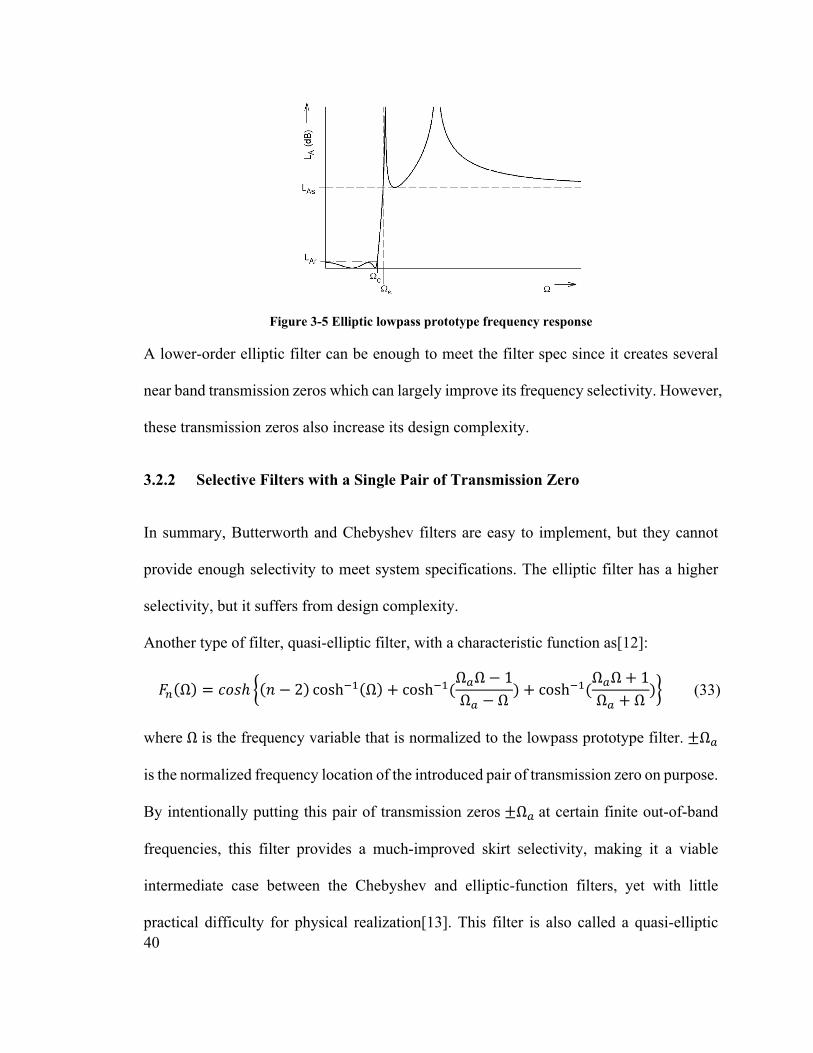
Figure [3-5] depicts an elliptic filter frequency response. The elliptic filter has a
complicated topology, but it could provide a very sharp frequency selectivity. For an
Elliptic filter, the characteristic function 𝐹𝐹𝑗𝑗 is a complicated elliptic function. It can
generate theoretically infinite transmission zeros at out-off-band frequency. Therefore, the
frequency selectivity will be improved. Its transfer function shows both an in-band ripple
and an out-of-band equal-ripple behavior.
40
Figure 3-5 Elliptic lowpass prototype frequency response
A lower-order elliptic filter can be enough to meet the filter spec since it creates several
near band transmission zeros which can largely improve its frequency selectivity. However,
these transmission zeros also increase its design complexity.
3.2.2 Selective Filters with a Single Pair of Transmission Zero
In summary, Butterworth and Chebyshev filters are easy to implement, but they cannot
provide enough selectivity to meet system specifications. The elliptic filter has a higher
selectivity, but it suffers from design complexity.
Another type of filter, quasi-elliptic filter, with a characteristic function as[12]:
𝐹𝐹𝑖𝑖(Ω) = 𝑐𝑐𝑓𝑓𝑠𝑠ℎ �(𝑗𝑗 − 2) cosh−1(Ω) + cosh−1(Ω𝑎𝑎Ω − 1Ω𝑎𝑎 − Ω
) + cosh−1(Ω𝑎𝑎Ω + 1Ω𝑎𝑎 + Ω
)� (33)
where Ω is the frequency variable that is normalized to the lowpass prototype filter. ±Ω𝑎𝑎
is the normalized frequency location of the introduced pair of transmission zero on purpose.
By intentionally putting this pair of transmission zeros ±Ω𝑎𝑎 at certain finite out-of-band
frequencies, this filter provides a much-improved skirt selectivity, making it a viable
intermediate case between the Chebyshev and elliptic-function filters, yet with little
practical difficulty for physical realization[13]. This filter is also called a quasi-elliptic

41
filter since it has only one pair of transmission zeros on finite frequency compared with
real elliptic filter. Some reference[14] also provides the design of this type of filter with
transmission zeros at both real and imaginary frequencies so it can improve both skirt
selectivity and flat in-band group delay.
Figure 3-6 Compare with Chebyshev and the filter with a signal pair of attenuation pole at finite
frequency.[15]
Figure [3-6] shows some typical frequency response of this type of filters for n = 6 and
LR = −20𝑑𝑑𝐵𝐵, with transmission zero at different offset frequency, as compared to that of
the same order Chebyshev filter. As can be seen, the improvement in selectivity over the
Chebyshev filter is evident. The closer the attenuation poles to the cut-off frequency, the
sharper the filter skirt, and the higher the selectivity.
3.3 Filter Synthesis
3.3.1 Lowpass prototype
A lowpass prototype circuit is a circuit network synthesized from the desired transfer
function. It provides the same frequency response as the transfer function mentioned above
42
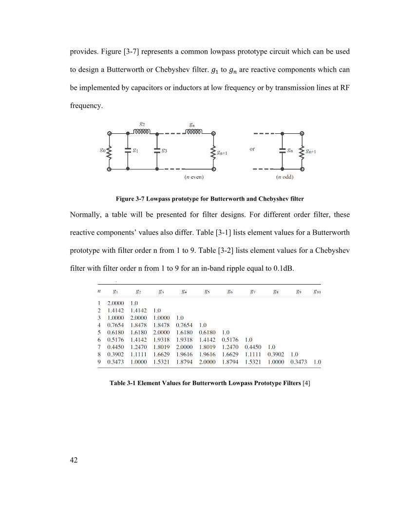
provides. Figure [3-7] represents a common lowpass prototype circuit which can be used
to design a Butterworth or Chebyshev filter. 𝐴𝐴1 to 𝐴𝐴𝑖𝑖 are reactive components which can
be implemented by capacitors or inductors at low frequency or by transmission lines at RF
frequency.
Figure 3-7 Lowpass prototype for Butterworth and Chebyshev filter
Normally, a table will be presented for filter designs. For different order filter, these
reactive components’ values also differ. Table [3-1] lists element values for a Butterworth
prototype with filter order n from 1 to 9. Table [3-2] lists element values for a Chebyshev
filter with filter order n from 1 to 9 for an in-band ripple equal to 0.1dB.
Table 3-1 Element Values for Butterworth Lowpass Prototype Filters [4]
43
Table 3-2 Element Values for Chebyshev Lowpass Prototype Filters [4]
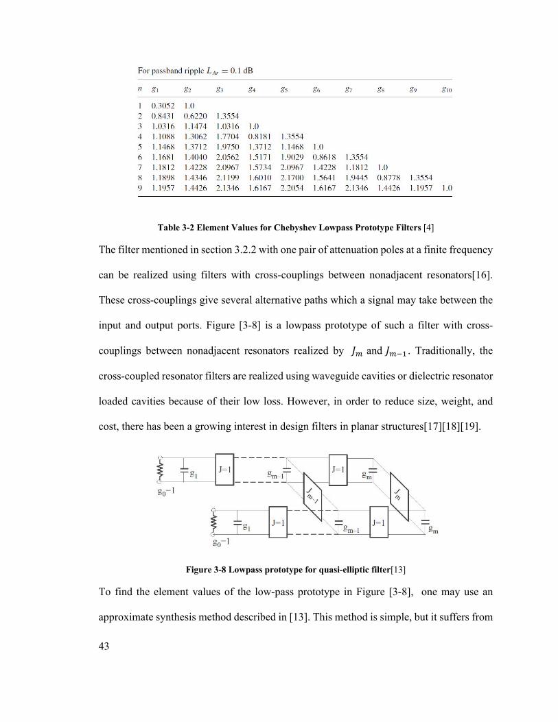
The filter mentioned in section 3.2.2 with one pair of attenuation poles at a finite frequency
can be realized using filters with cross-couplings between nonadjacent resonators[16].
These cross-couplings give several alternative paths which a signal may take between the
input and output ports. Figure [3-8] is a lowpass prototype of such a filter with cross-
couplings between nonadjacent resonators realized by 𝐽𝐽𝑚𝑚 and 𝐽𝐽𝑚𝑚−1 . Traditionally, the
cross-coupled resonator filters are realized using waveguide cavities or dielectric resonator
loaded cavities because of their low loss. However, in order to reduce size, weight, and
cost, there has been a growing interest in design filters in planar structures[17][18][19].
Figure 3-8 Lowpass prototype for quasi-elliptic filter[13]
To find the element values of the low-pass prototype in Figure [3-8], one may use an
approximate synthesis method described in [13]. This method is simple, but it suffers from
44
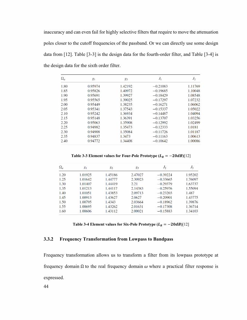
inaccuracy and can even fail for highly selective filters that require to move the attenuation
poles closer to the cutoff frequencies of the passband. Or we can directly use some design
data from [12]. Table [3-3] is the design data for the fourth-order filter, and Table [3-4] is
the design data for the sixth order filter.
Table 3-3 Element values for Four-Pole Prototype (𝑳𝑳𝑳𝑳 = −𝟐𝟐𝟐𝟐𝟐𝟐𝟐𝟐)[12]
Table 3-4 Element values for Six-Pole Prototype (𝑳𝑳𝑳𝑳 = −𝟐𝟐𝟐𝟐𝟐𝟐𝟐𝟐)[12]
3.3.2 Frequency Transformation from Lowpass to Bandpass
Frequency transformation allows us to transform a filter from its lowpass prototype at
frequency domain Ω to the real frequency domain 𝑗𝑗 where a practical filter response is
expressed.
45
Through frequency transformation, a lowpass filter prototype with normalized frequency
Ω can be transformed to the desired bandpass filter centered at 𝑗𝑗0 by equation:
Ω =1
𝐹𝐹𝐵𝐵𝑊𝑊(𝑗𝑗𝑗𝑗0
−𝑗𝑗0
𝑗𝑗) (34)
in which 𝑗𝑗 is the frequency variable of the bandpass filter, and 𝐹𝐹𝐵𝐵𝑊𝑊 is the fractional
bandwidth of the bandpass filter. 𝐹𝐹𝐵𝐵𝑊𝑊 and 𝑗𝑗0 can be defined by the equation:
𝐹𝐹𝐵𝐵𝑊𝑊 =𝑗𝑗2 − 𝑗𝑗1𝑗𝑗0
(35)
𝑗𝑗0 = �𝑗𝑗1𝑗𝑗2 (36)
𝑗𝑗1 and 𝑗𝑗2 are the lower and higher edge of the bandpass filter.
For the quasi-elliptic filter lowpass prototype, the transmission zero ±Ω𝑎𝑎 are mapped to
two real frequency zeros by:
𝑗𝑗𝑎𝑎1 = 𝑗𝑗0−Ω𝑎𝑎𝐹𝐹𝐵𝐵𝑊𝑊 + �(Ω𝑎𝑎𝐹𝐹𝐵𝐵𝑊𝑊)2 + 4
2 (37)
𝑗𝑗𝑎𝑎2 = 𝑗𝑗0Ω𝑎𝑎𝐹𝐹𝐵𝐵𝑊𝑊 + �(Ω𝑎𝑎𝐹𝐹𝐵𝐵𝑊𝑊)2 + 4
2 (38)
The inductive/capacitive element g in the lowpass prototype will transform to a
series/parallel LC resonant circuit in the bandpass filter. The elements for the series LC
resonator in the bandpass filter are:
𝐿𝐿𝑠𝑠 = �Ω𝑐𝑐
𝐹𝐹𝐵𝐵𝑊𝑊𝑗𝑗0�𝑍𝑍0𝐴𝐴 (39)
𝐶𝐶𝑠𝑠 = �𝐹𝐹𝐵𝐵𝑊𝑊𝑗𝑗0Ω𝑐𝑐
�1𝑍𝑍0𝐴𝐴
(40)
And the elements for the parallel LC resonator in the bandpass filter are:
46
𝐶𝐶𝑝𝑝 = �Ω𝑐𝑐
𝐹𝐹𝐵𝐵𝑊𝑊𝑗𝑗0�𝐴𝐴𝑍𝑍0
(41)
𝐿𝐿𝑝𝑝 = �𝐹𝐹𝐵𝐵𝑊𝑊𝑗𝑗0Ω𝑐𝑐
�𝑍𝑍0𝐴𝐴
(42)
The element transformation is shown in Figure [3-9]. Each reactive component is converted
to a resonator through bandpass transformation. According to equation (18) in chapter 2, a
series resonator can be replaced by a half-wavelength short-end transmission line and a
parallel resonator can be replaced by a half-wavelength open-end transmission line.
Figure 3-9 Lowpass prototype to bandpass transformation
3.3.3 Coupling theory for filter design
Coupled-resonator circuits are of importance for the design of RF/microwave filters. It is
a very simple technique for designing coupled-resonator filters, and it can be applied to
any type of resonator despite its physical structure. It can be used to design waveguide
filters, dielectric resonator filters, microstrip filters, and so on. This design method is based
on coupling coefficients of each two nearby resonators and the external quality factors of
47
the input and output resonators. It is extremely useful for the narrow-band bandpass filter
design.
Figure [3-10] shows an equivalent circuit of a coupled-resonator circuit. It can represent
most types of bandpass filters. The coupling coefficient between the 𝑗𝑗 and 𝑚𝑚 parallel
resonator is represented by 𝑀𝑀𝑖𝑖𝑚𝑚.
Figure 3-10 Equivalent circuits of n-coupled resonators circuit
The relation between its loop current and voltage is described by a general coupling matrix
[A] [15].
[𝐴𝐴] =
⎣⎢⎢⎢⎢⎢⎢⎡
1𝑄𝑄𝑒𝑒𝑖𝑖 ∙ 𝐹𝐹𝐵𝐵𝑊𝑊
+ 𝑝𝑝 −𝑗𝑗𝑀𝑀12
𝐹𝐹𝐵𝐵𝑊𝑊⋯ −
𝑗𝑗𝑀𝑀1𝑖𝑖
𝐹𝐹𝐵𝐵𝑊𝑊
−𝑗𝑗𝑀𝑀21
𝐹𝐹𝐵𝐵𝑊𝑊𝑝𝑝 ⋯ −
𝑗𝑗𝑀𝑀2𝑖𝑖
𝐹𝐹𝐵𝐵𝑊𝑊⋮ ⋮ ⋮ ⋮
−𝑗𝑗𝑀𝑀𝑖𝑖1
𝐹𝐹𝐵𝐵𝑊𝑊−𝑗𝑗𝑀𝑀𝑖𝑖1
𝐹𝐹𝐵𝐵𝑊𝑊⋯ 1
𝑄𝑄𝑒𝑒𝑖𝑖 ∙ 𝐹𝐹𝐵𝐵𝑊𝑊 + 𝑝𝑝
⎦⎥⎥⎥⎥⎥⎥⎤
(43)
Where:
p = j1
𝐹𝐹𝐵𝐵𝑊𝑊�𝑗𝑗𝑗𝑗0
−𝑗𝑗0
𝑗𝑗� (44)
𝑅𝑅𝑗𝑗0𝐿𝐿
=1𝑄𝑄𝑒𝑒𝑖𝑖
(45)
𝑀𝑀𝑖𝑖𝑖𝑖 =𝐿𝐿𝑖𝑖𝑖𝑖𝐿𝐿
(46)
48
For any type of bandpass filter, this general coupling matrix can be derived, and it can fully
describe the filter performance. Also, each parameter in the coupling matrix can be
obtained from the filter’s lowpass prototype parameters.
For Butterworth and Chebyshev lowpass prototypes, the relation between the coupling
matrix and the lowpass prototype components are:
𝑄𝑄𝑒𝑒𝑖𝑖 =𝐴𝐴0𝐴𝐴1𝐹𝐹𝐵𝐵𝑊𝑊
(47)
𝑄𝑄𝑒𝑒𝑖𝑖 =𝐴𝐴𝑖𝑖𝐴𝐴𝑖𝑖+1𝐹𝐹𝐵𝐵𝑊𝑊
(48)
𝑀𝑀𝑖𝑖,𝑖𝑖+1 =𝐹𝐹𝐵𝐵𝑊𝑊�𝐴𝐴𝑖𝑖𝐴𝐴𝑖𝑖+1
(49)
𝑄𝑄𝑒𝑒𝑖𝑖 and 𝑄𝑄𝑒𝑒𝑖𝑖 are called external quality factors. It represents the coupling strength between
the circuit network and I/O ports. 𝑀𝑀𝑖𝑖,𝑖𝑖+1 represents the coupling coefficient between every
two resonators. For a quasi-elliptic filter, the relationship of the coupling matrix and a
lowpass prototype is given by:
𝑄𝑄𝑒𝑒1 = 𝑄𝑄𝑒𝑒𝑗𝑗 =𝐴𝐴1
𝐹𝐹𝐵𝐵𝑊𝑊 (50)
𝑀𝑀𝑖𝑖,𝑖𝑖+1 = 𝑀𝑀𝑖𝑖−𝑖𝑖,𝑖𝑖−𝑖𝑖+1 =𝐹𝐹𝐵𝐵𝑊𝑊�𝐴𝐴𝑖𝑖𝐴𝐴𝑖𝑖+1
𝑓𝑓𝑓𝑓𝑓𝑓 𝑅𝑅 = 1 𝑡𝑡𝑓𝑓 𝑚𝑚− 1,𝑚𝑚 =𝑗𝑗2
(51)
𝑀𝑀𝑚𝑚,𝑚𝑚+1 =𝐹𝐹𝐵𝐵𝑊𝑊 ∗ 𝐽𝐽𝑚𝑚
𝐴𝐴𝑚𝑚 (52)
𝑀𝑀𝑚𝑚−1,𝑚𝑚+2 =𝐹𝐹𝐵𝐵𝑊𝑊 ∗ 𝐽𝐽𝑚𝑚−1
𝐴𝐴𝑚𝑚−1 (53)
A general coupling structure for the quasi-elliptic filter is depicted in Figure [3-11], where
each node represents a resonator in Figure [3-10], the full lines indicate the main path
49
couplings, and the broken line denotes the cross-coupling. It is essential that the phase of
cross-coupling 𝑀𝑀𝑚𝑚−1,𝑚𝑚+2 has a 180-degree shift to the phase of 𝑀𝑀𝑚𝑚,𝑚𝑚+1 to achieve a pair
of attenuation poles at finite frequencies, where 𝑚𝑚 = 𝑁𝑁/2 with 𝑁𝑁 being the degree of the
filter. This can be achieved by electric coupling on one line and magnetic coupling on
another line. Both the electric coupling and magnetic coupling can be simulated by the full-
wave electromagnetic (EM) simulation.
Figure 3-11 General Coupling structure for a bandpass filter with a pair of transmission zero
The advantage of using coupling theory for narrow bandwidth bandpass filter design is that
coupling coefficient between every two resonators and external quality factors between the
port with the filter structure are directly related to each resonators’ physical dimension and
tapped line position. Those parameters can be easily derived from an EM simulation result.
3.4 Summary
Millimeter wave band 5G communication systems require high-performance narrow-band
bandpass filters having low insertion loss and high selectivity together with linear phase or
flat group delay in the passband. In this chapter, some generic filter types are present, and
their advantages and disadvantages are analyzed. The coupling theory method for bandpass

50
filter design is also presented. The next chapter will present filter designs that are
constructed by this method.
51
Chapter 4: Filter Implementation
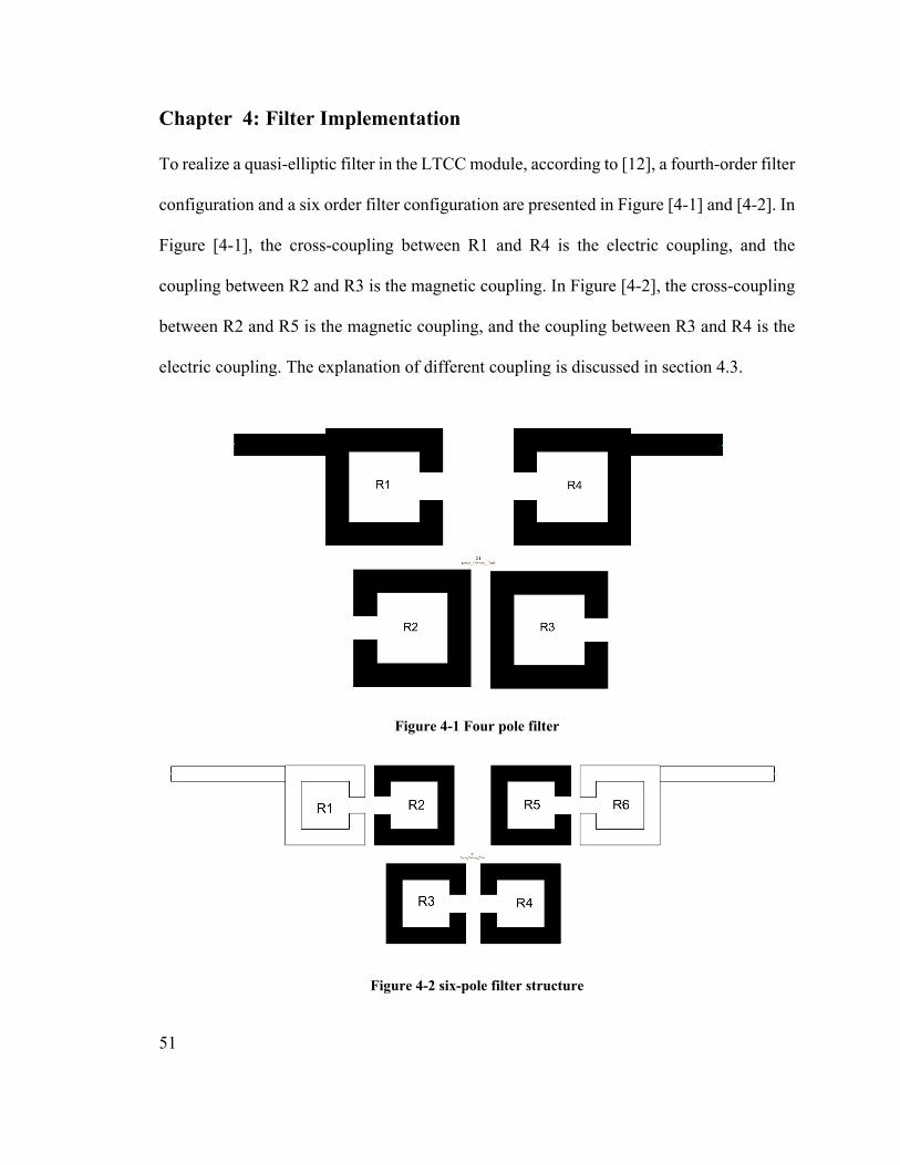
To realize a quasi-elliptic filter in the LTCC module, according to [12], a fourth-order filter
configuration and a six order filter configuration are presented in Figure [4-1] and [4-2]. In
Figure [4-1], the cross-coupling between R1 and R4 is the electric coupling, and the
coupling between R2 and R3 is the magnetic coupling. In Figure [4-2], the cross-coupling
between R2 and R5 is the magnetic coupling, and the coupling between R3 and R4 is the
electric coupling. The explanation of different coupling is discussed in section 4.3.
Figure 4-1 Four pole filter
Figure 4-2 six-pole filter structure
52
Design parameters for these two filters can be derived from system specs from Table [2-
5]. Based on these specs, a quasi-elliptic lowpass prototype is first chosen from Table [3-
3] and Table [3-4]. Here a four-pole lowpass prototype with transmission zero Ω𝑎𝑎 = 1.8
and a six-pole lowpass prototype with transmission zero Ω𝑎𝑎 = 1.2 are selected. Equation
(50)-(53) convert these lowpass prototype parameters into external quality factors and
coupling coefficients.
Design parameters for four pole filter:
𝑀𝑀1,2 = 𝑀𝑀3,4 = 0.06 (54)
𝑀𝑀2,3 = 0.055 (55)
𝑀𝑀1,4= − 0.015 (56)
𝑄𝑄𝑒𝑒𝑖𝑖 = 𝑄𝑄𝑒𝑒𝑜𝑜 = 13 (57)
Design parameters for six pole filter:
𝑀𝑀1,2 = 𝑀𝑀5,6 = 0.058 (58)
𝑀𝑀2,3 = 𝑀𝑀4,5 = 0.041 (59)
𝑀𝑀3,4 = 0.047 (60)
𝑀𝑀2,5 = −.0.007 (61)
𝑄𝑄𝑒𝑒𝑖𝑖 = 𝑄𝑄𝑒𝑒𝑜𝑜 = 14 (62)
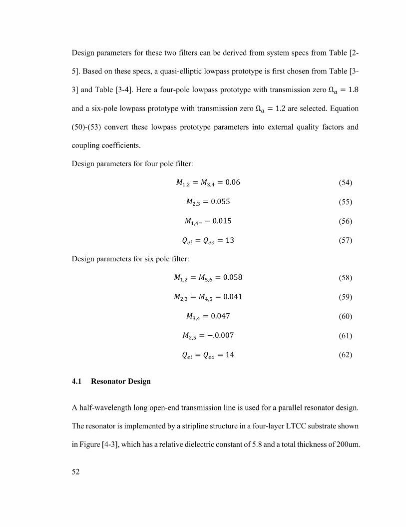
4.1 Resonator Design
A half-wavelength long open-end transmission line is used for a parallel resonator design.
The resonator is implemented by a stripline structure in a four-layer LTCC substrate shown
in Figure [4-3], which has a relative dielectric constant of 5.8 and a total thickness of 200um.
53
The conductor metal thickness is 10um. Figure [4-4] shows a folded half-wavelength
square loop.
Figure 4-3 LTCC substrate structure
Figure 4-4 folded half-wavelength resonator
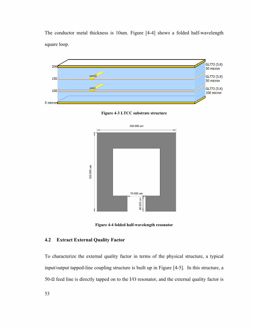
4.2 Extract External Quality Factor
To characterize the external quality factor in terms of the physical structure, a typical
input/output tapped-line coupling structure is built up in Figure [4-5]. In this structure, a
50-Ω feed line is directly tapped on to the I/O resonator, and the external quality factor is
54
controlled by the tapping position T. As the distance gets shorter, the tapped line is closer
to the virtual ground of the resonator.
Figure 4-5 tapped-line coupling structure
By performing a network analysis and making a narrow band approximation, the relation
between external quality factor and return loss 𝑆𝑆11 can be derived[15]:
𝑆𝑆11 =1 − 𝑗𝑗𝑄𝑄𝑒𝑒 ∙ (2∆𝑗𝑗/𝑗𝑗0) 1 + 𝑗𝑗𝑄𝑄𝑒𝑒 ∙ (2∆𝑗𝑗/𝑗𝑗0)
(63)
Assume that the resonator is lossless, the phase response of 𝑆𝑆11 vary with frequency. Figure
[4-6(a)] shows that the phase response of 𝑆𝑆11 is a function of ∆𝑗𝑗/𝑗𝑗0. When the phase is
±90𝑜𝑜 the corresponding value of ∆𝑗𝑗 is found to be:
2𝑄𝑄𝑒𝑒∆𝑗𝑗±
𝑗𝑗𝑜𝑜= ∓1 (64)
And the external quality factor can be extracted from the relation:
Qe =ω0
∆ω±90o (65)
By adjusting the tapped-line position and measuring each phase response, the relation
between external quality factor and tapped line position is depicted in Figure [4-6(b)].
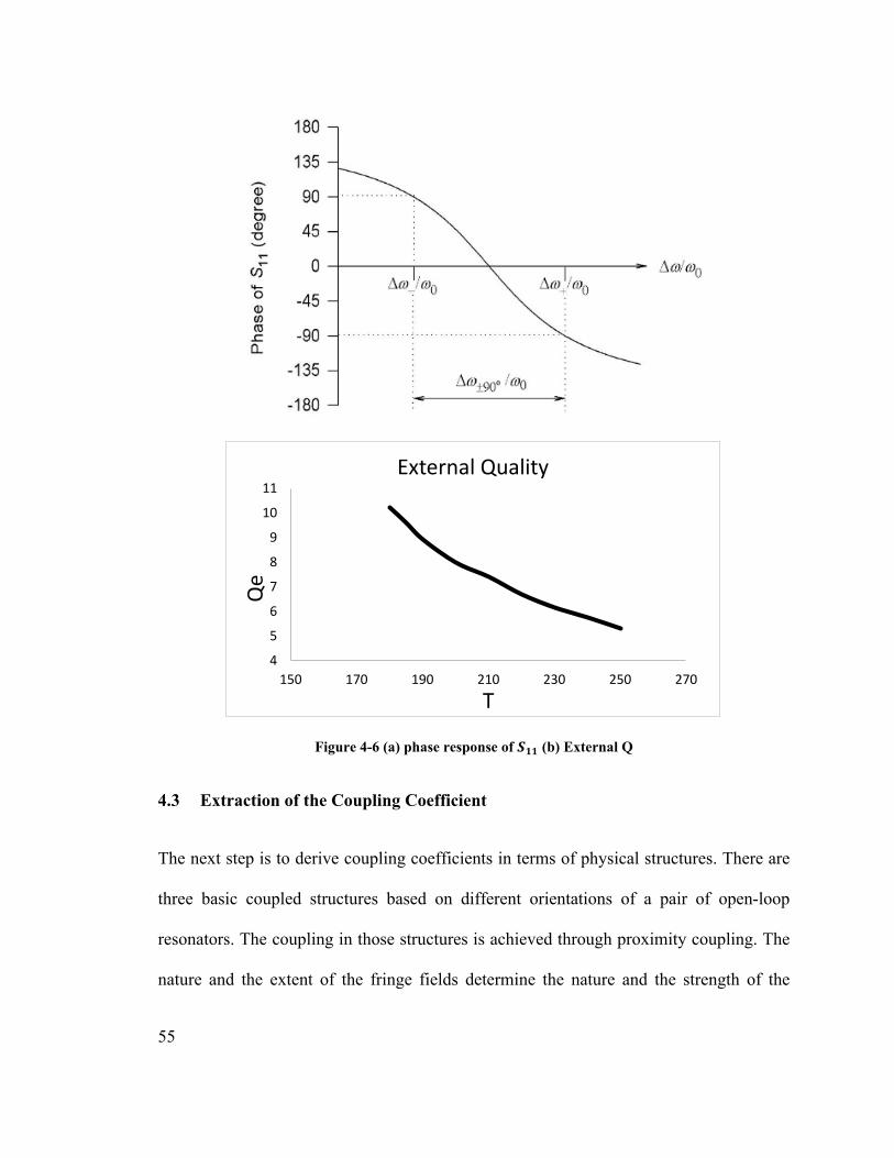
55
Figure 4-6 (a) phase response of 𝑺𝑺𝑺𝑺𝑺𝑺 (b) External Q
4.3 Extraction of the Coupling Coefficient
The next step is to derive coupling coefficients in terms of physical structures. There are
three basic coupled structures based on different orientations of a pair of open-loop
resonators. The coupling in those structures is achieved through proximity coupling. The
nature and the extent of the fringe fields determine the nature and the strength of the
4
5
6
7
8
9
10
11
150 170 190 210 230 250 270
Qe
T
External Quality
56
coupling effect. Because the fringe field exhibits an exponentially decaying character
outside the region, the electric fringe fields are stronger near the side with maximum
electric field distribution, whereas the magnetic fringe field is stronger near the side having
the maximum magnetic field distribution[15]. The coupling coefficient can be extracted
from its frequency response through an EM simulation.
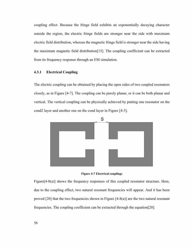
4.3.1 Electrical Coupling
The electric coupling can be obtained by placing the open sides of two coupled resonators
closely, as in Figure [4-7]. The coupling can be purely planar, or it can be both planar and
vertical. The vertical coupling can be physically achieved by putting one resonator on the
cond2 layer and another one on the cond layer in Figure [4-3].
Figure 4-7 Electrical couplings
Figure[4-8(a)] shows the frequency responses of this coupled resonator structure. Here,
due to the coupling effect, two natural resonant frequencies will appear. And it has been
proved [20] that the two frequencies shown in Figure [4-8(a)] are the two natural resonant
frequencies. The coupling coefficient can be extracted through the equation[20]:
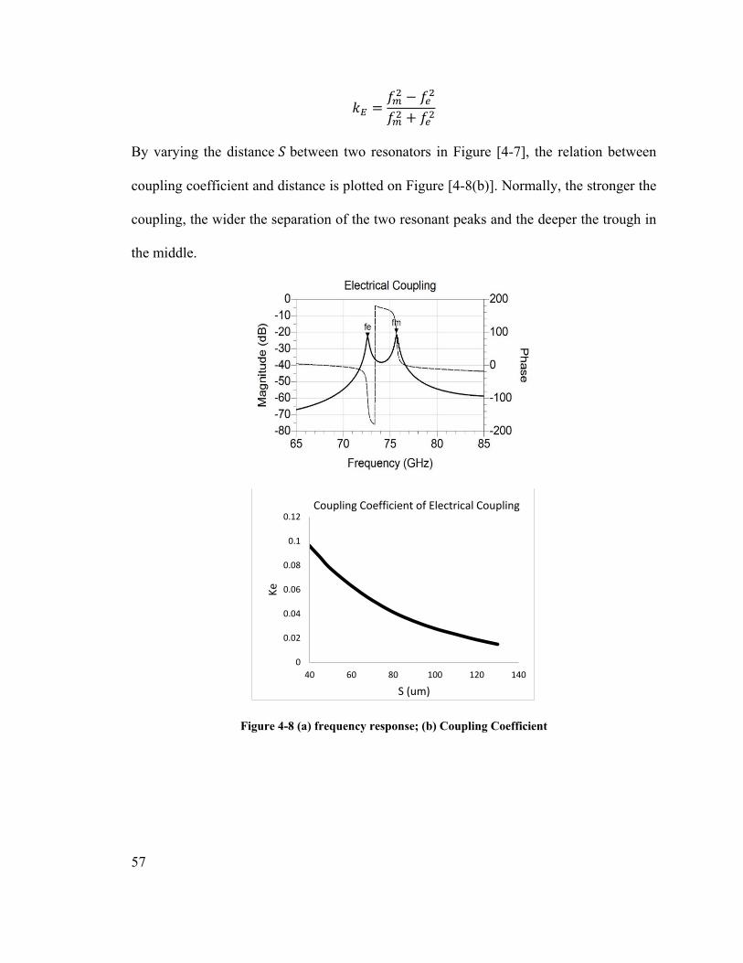
57
𝑘𝑘𝐸𝐸 =𝑓𝑓𝑚𝑚2 − 𝑓𝑓𝑒𝑒2
𝑓𝑓𝑚𝑚2 + 𝑓𝑓𝑒𝑒2
By varying the distance 𝑆𝑆 between two resonators in Figure [4-7], the relation between
coupling coefficient and distance is plotted on Figure [4-8(b)]. Normally, the stronger the
coupling, the wider the separation of the two resonant peaks and the deeper the trough in
the middle.
Figure 4-8 (a) frequency response; (b) Coupling Coefficient
0
0.02
0.04
0.06
0.08
0.1
0.12
40 60 80 100 120 140
Ke
S (um)
Coupling Coefficient of Electrical Coupling
58
4.3.2 Magnetic Coupling
Like the electric coupling, the magnetic coupling can also be obtained by placing the
maximum magnetic field sides of two coupled resonators closely, as shown in Figure [4-
9]. The equation used to extract the coupling coefficient is:
𝑘𝑘𝑀𝑀 =𝑓𝑓𝑒𝑒2 − 𝑓𝑓𝑚𝑚2
𝑓𝑓𝑒𝑒2 + 𝑓𝑓𝑚𝑚2
Figure 4-9 Magnetic Coupling
Figure[4-10(a)] is the frequency response of this coupled resonator structure, and the
relation between coupling coefficient and distance is extracted in Figure [4-10(b)]. By
comparing the phase responses of Figures [4-8(a)] and Figure [4-10(a)], it can be observed
that these two structures phase response in Figure [4-8(a)] and Figure [4-10(a)] are indeed
out of phase.
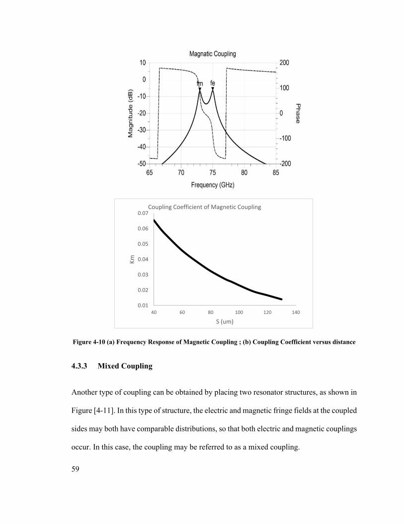
59
Figure 4-10 (a) Frequency Response of Magnetic Coupling ; (b) Coupling Coefficient versus distance
4.3.3 Mixed Coupling
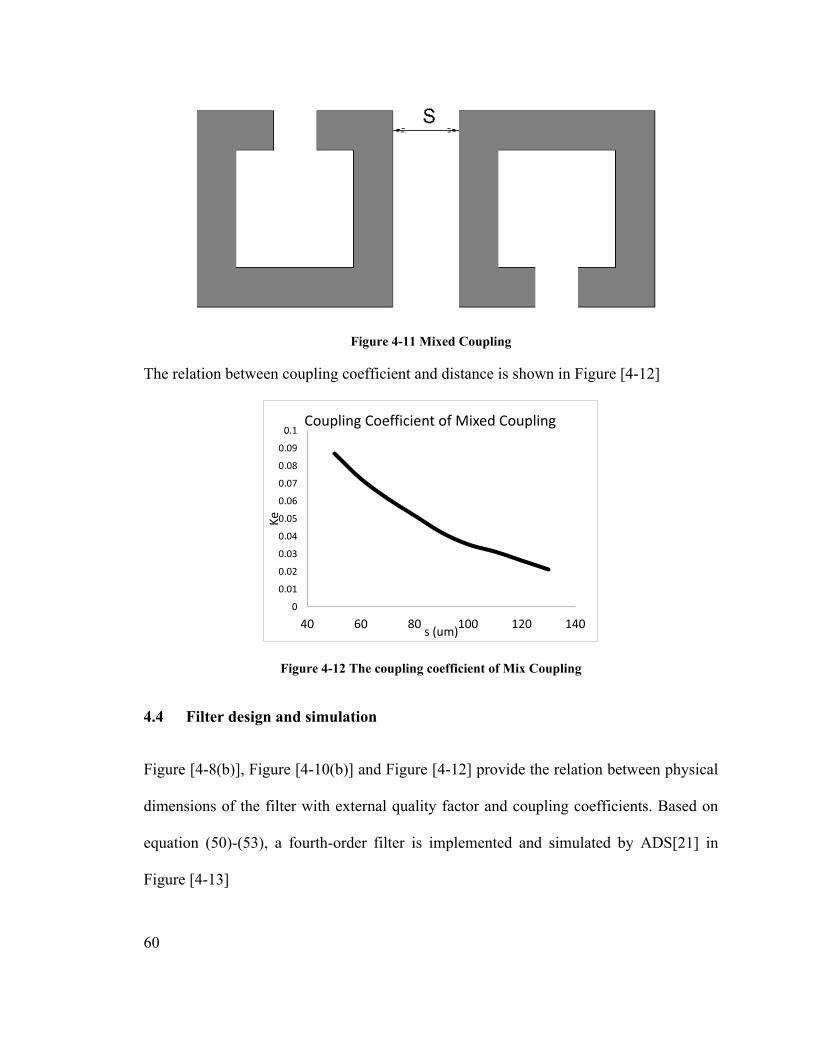
Another type of coupling can be obtained by placing two resonator structures, as shown in
Figure [4-11]. In this type of structure, the electric and magnetic fringe fields at the coupled
sides may both have comparable distributions, so that both electric and magnetic couplings
occur. In this case, the coupling may be referred to as a mixed coupling.
0.01
0.02
0.03
0.04
0.05
0.06
0.07
40 60 80 100 120 140
Km
S (um)
Coupling Coefficient of Magnetic Coupling
60
Figure 4-11 Mixed Coupling
The relation between coupling coefficient and distance is shown in Figure [4-12]
Figure 4-12 The coupling coefficient of Mix Coupling
4.4 Filter design and simulation
Figure [4-8(b)], Figure [4-10(b)] and Figure [4-12] provide the relation between physical
dimensions of the filter with external quality factor and coupling coefficients. Based on
equation (50)-(53), a fourth-order filter is implemented and simulated by ADS[21] in
Figure [4-13]
0
0.01
0.02
0.03
0.04
0.05
0.06
0.07
0.08
0.09
0.1
40 60 80 100 120 140
Ke
s (um)
Coupling Coefficient of Mixed Coupling
61
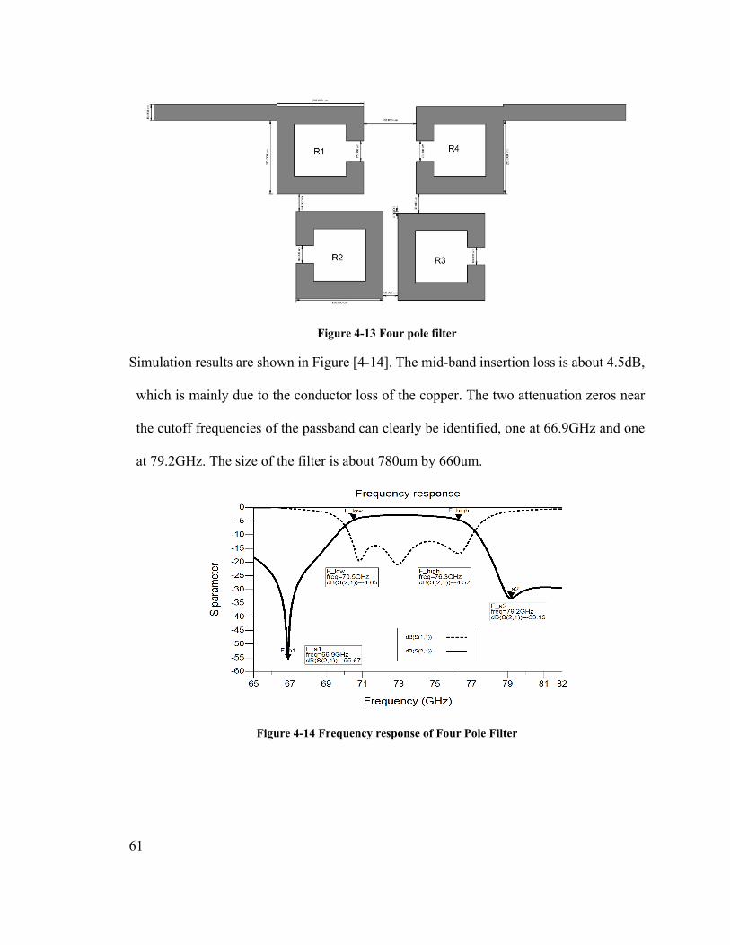
Figure 4-13 Four pole filter
Simulation results are shown in Figure [4-14]. The mid-band insertion loss is about 4.5dB,
which is mainly due to the conductor loss of the copper. The two attenuation zeros near
the cutoff frequencies of the passband can clearly be identified, one at 66.9GHz and one
at 79.2GHz. The size of the filter is about 780um by 660um.
Figure 4-14 Frequency response of Four Pole Filter
62
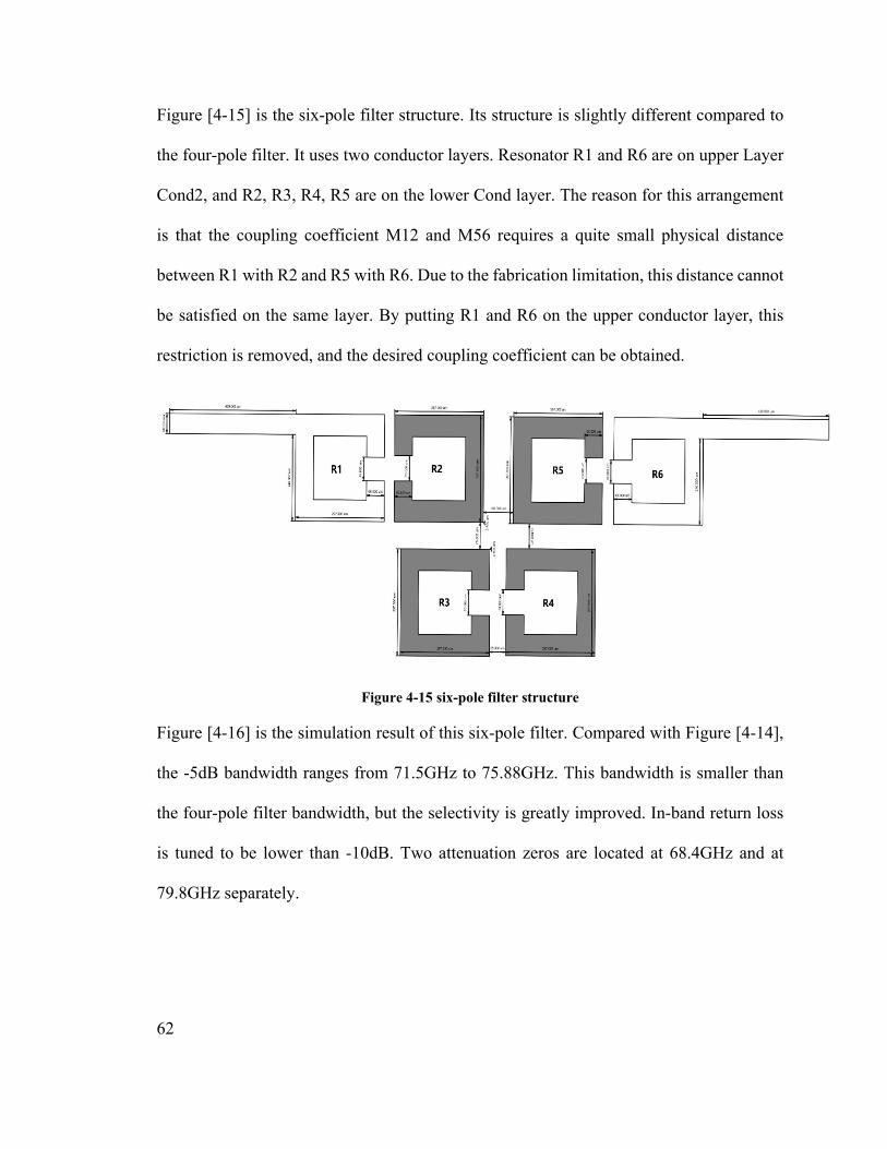
Figure [4-15] is the six-pole filter structure. Its structure is slightly different compared to
the four-pole filter. It uses two conductor layers. Resonator R1 and R6 are on upper Layer
Cond2, and R2, R3, R4, R5 are on the lower Cond layer. The reason for this arrangement
is that the coupling coefficient M12 and M56 requires a quite small physical distance
between R1 with R2 and R5 with R6. Due to the fabrication limitation, this distance cannot
be satisfied on the same layer. By putting R1 and R6 on the upper conductor layer, this
restriction is removed, and the desired coupling coefficient can be obtained.
Figure 4-15 six-pole filter structure
Figure [4-16] is the simulation result of this six-pole filter. Compared with Figure [4-14],
the -5dB bandwidth ranges from 71.5GHz to 75.88GHz. This bandwidth is smaller than
the four-pole filter bandwidth, but the selectivity is greatly improved. In-band return loss
is tuned to be lower than -10dB. Two attenuation zeros are located at 68.4GHz and at
79.8GHz separately.
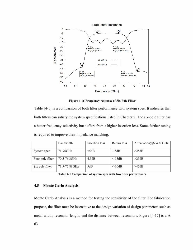
63
Figure 4-16 Frequency response of Six Pole Filter
Table [4-1] is a comparison of both filter performance with system spec. It indicates that
both filters can satisfy the system specifications listed in Chapter 2. The six-pole filter has
a better frequency selectivity but suffers from a higher insertion loss. Some further tuning
is required to improve their impedance matching.
Bandwidth Insertion loss Return loss Attenuation@68&80GHz
System spec 71-76GHz <5dB -15dB >25dB
Four pole filter 70.5-76.3GHz 4.5dB <-15dB >25dB
Six pole filter 71.5-75.88GHz 5dB <-10dB >45dB
Table 4-1 Comparison of system spec with two filter performance
4.5 Monte Carlo Analysis
Monte Carlo Analysis is a method for testing the sensitivity of the filter. For fabrication
purpose, the filter must be insensitive to the design variation of design parameters such as
metal width, resonator length, and the distance between resonators. Figure [4-17] is a A
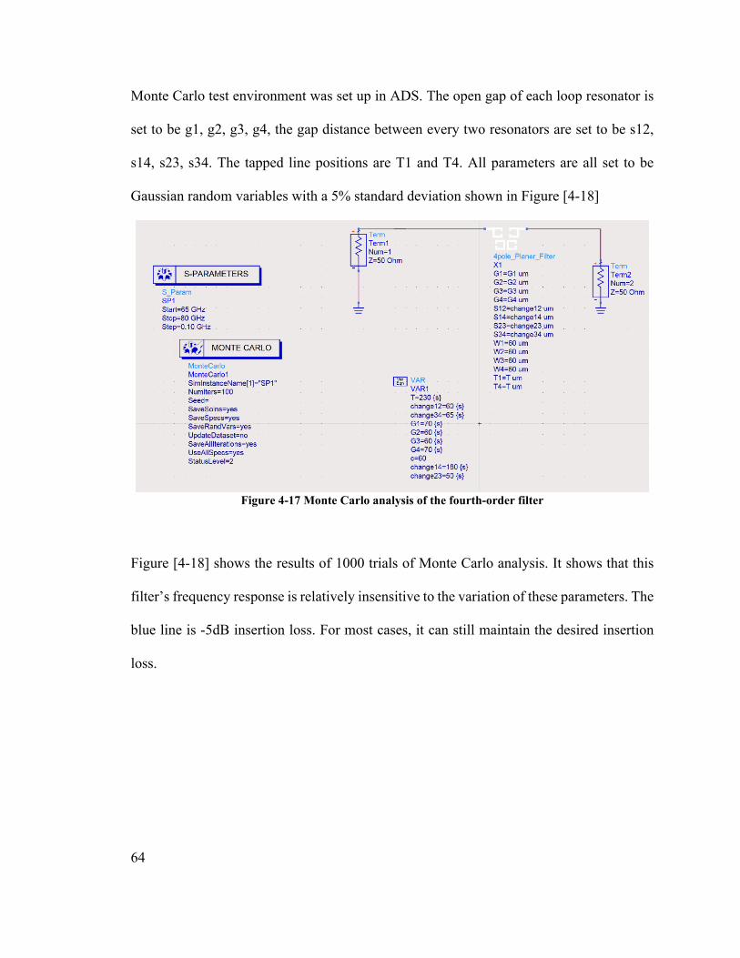
64
Monte Carlo test environment was set up in ADS. The open gap of each loop resonator is
set to be g1, g2, g3, g4, the gap distance between every two resonators are set to be s12,
s14, s23, s34. The tapped line positions are T1 and T4. All parameters are all set to be
Gaussian random variables with a 5% standard deviation shown in Figure [4-18]
Figure 4-17 Monte Carlo analysis of the fourth-order filter
Figure [4-18] shows the results of 1000 trials of Monte Carlo analysis. It shows that this
filter’s frequency response is relatively insensitive to the variation of these parameters. The
blue line is -5dB insertion loss. For most cases, it can still maintain the desired insertion
loss.
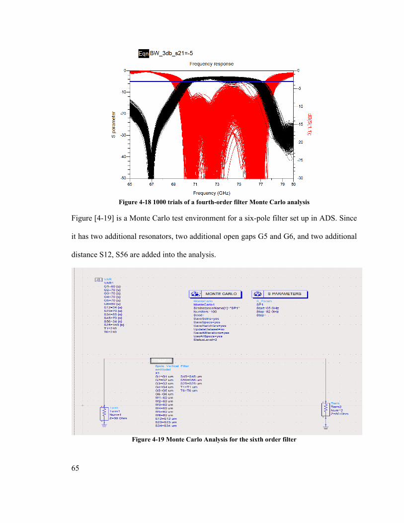
65
Figure 4-18 1000 trials of a fourth-order filter Monte Carlo analysis
Figure [4-19] is a Monte Carlo test environment for a six-pole filter set up in ADS. Since
it has two additional resonators, two additional open gaps G5 and G6, and two additional
distance S12, S56 are added into the analysis.
Figure 4-19 Monte Carlo Analysis for the sixth order filter
66
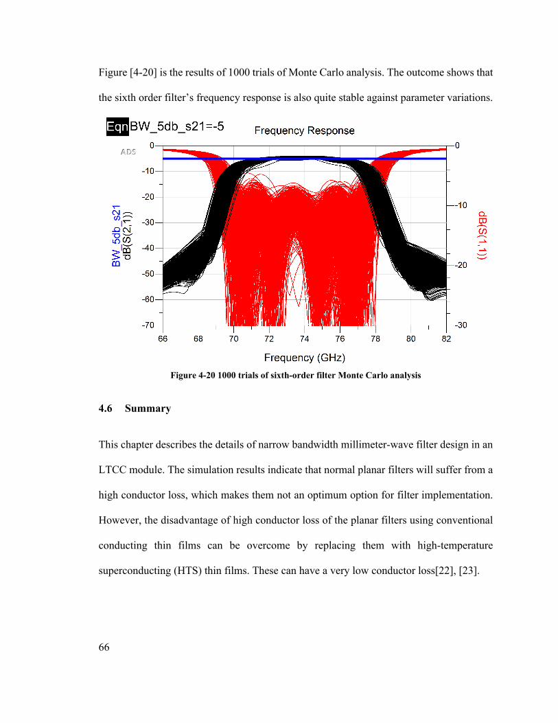
Figure [4-20] is the results of 1000 trials of Monte Carlo analysis. The outcome shows that
the sixth order filter’s frequency response is also quite stable against parameter variations.
Figure 4-20 1000 trials of sixth-order filter Monte Carlo analysis
4.6 Summary
This chapter describes the details of narrow bandwidth millimeter-wave filter design in an
LTCC module. The simulation results indicate that normal planar filters will suffer from a
high conductor loss, which makes them not an optimum option for filter implementation.
However, the disadvantage of high conductor loss of the planar filters using conventional
conducting thin films can be overcome by replacing them with high-temperature
superconducting (HTS) thin films. These can have a very low conductor loss[22], [23].
67
Chapter 5: Measurement
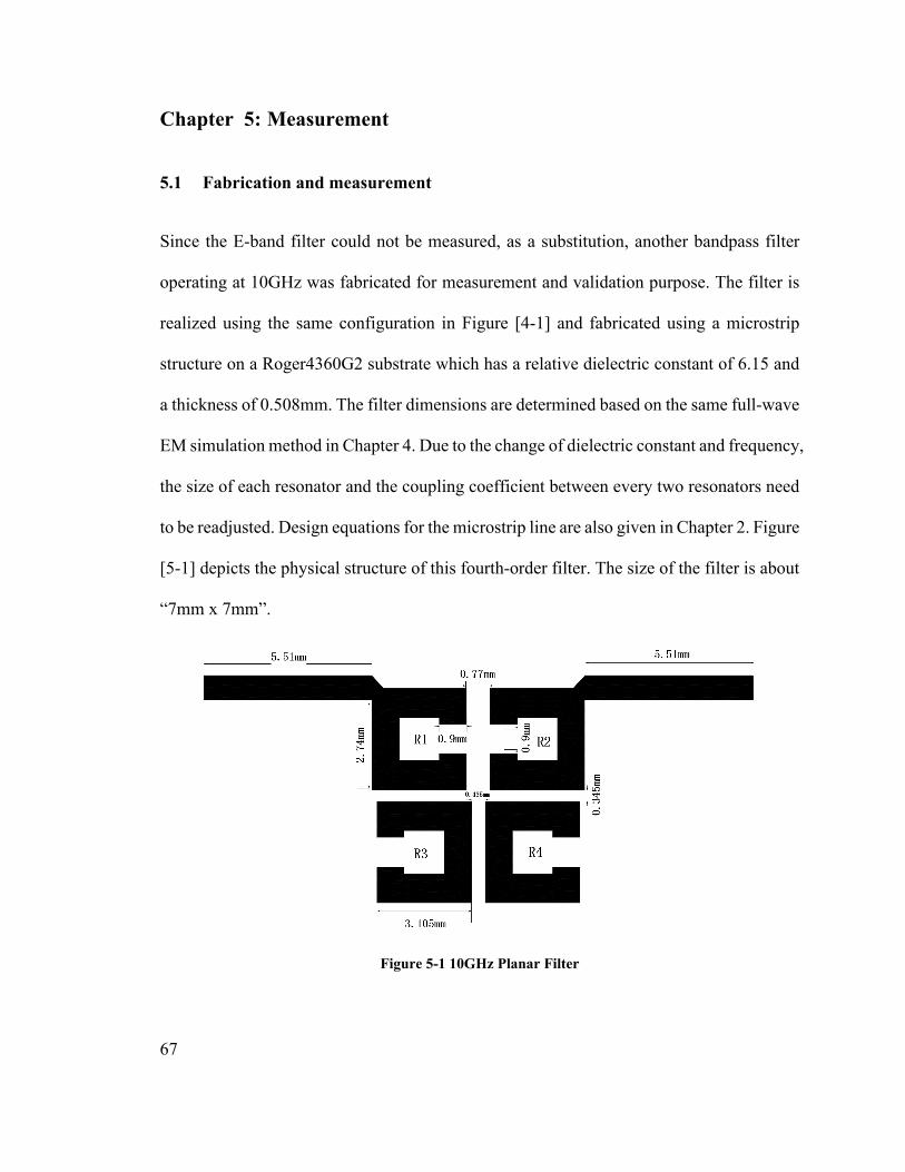
5.1 Fabrication and measurement
Since the E-band filter could not be measured, as a substitution, another bandpass filter
operating at 10GHz was fabricated for measurement and validation purpose. The filter is
realized using the same configuration in Figure [4-1] and fabricated using a microstrip
structure on a Roger4360G2 substrate which has a relative dielectric constant of 6.15 and
a thickness of 0.508mm. The filter dimensions are determined based on the same full-wave
EM simulation method in Chapter 4. Due to the change of dielectric constant and frequency,
the size of each resonator and the coupling coefficient between every two resonators need
to be readjusted. Design equations for the microstrip line are also given in Chapter 2. Figure
[5-1] depicts the physical structure of this fourth-order filter. The size of the filter is about
“7mm x 7mm”.
Figure 5-1 10GHz Planar Filter
68
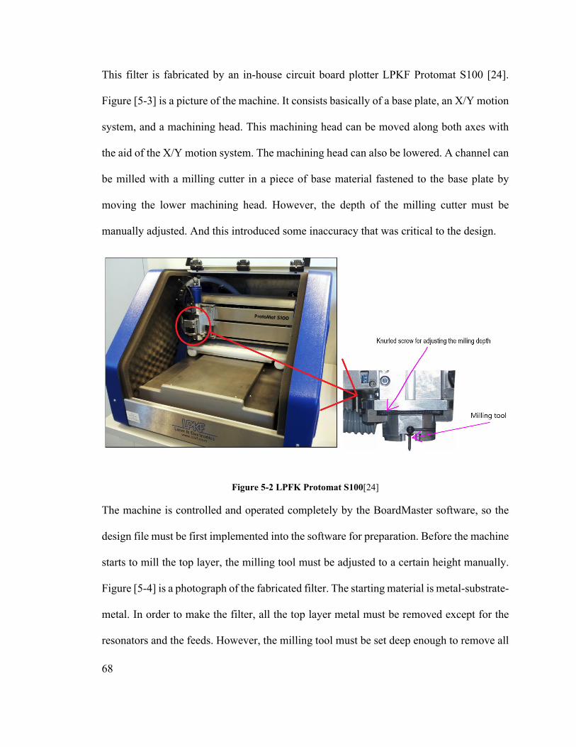
This filter is fabricated by an in-house circuit board plotter LPKF Protomat S100 [24].
Figure [5-3] is a picture of the machine. It consists basically of a base plate, an X/Y motion
system, and a machining head. This machining head can be moved along both axes with
the aid of the X/Y motion system. The machining head can also be lowered. A channel can
be milled with a milling cutter in a piece of base material fastened to the base plate by
moving the lower machining head. However, the depth of the milling cutter must be
manually adjusted. And this introduced some inaccuracy that was critical to the design.
Figure 5-2 LPFK Protomat S100[24]
The machine is controlled and operated completely by the BoardMaster software, so the
design file must be first implemented into the software for preparation. Before the machine
starts to mill the top layer, the milling tool must be adjusted to a certain height manually.
Figure [5-4] is a photograph of the fabricated filter. The starting material is metal-substrate-
metal. In order to make the filter, all the top layer metal must be removed except for the
resonators and the feeds. However, the milling tool must be set deep enough to remove all
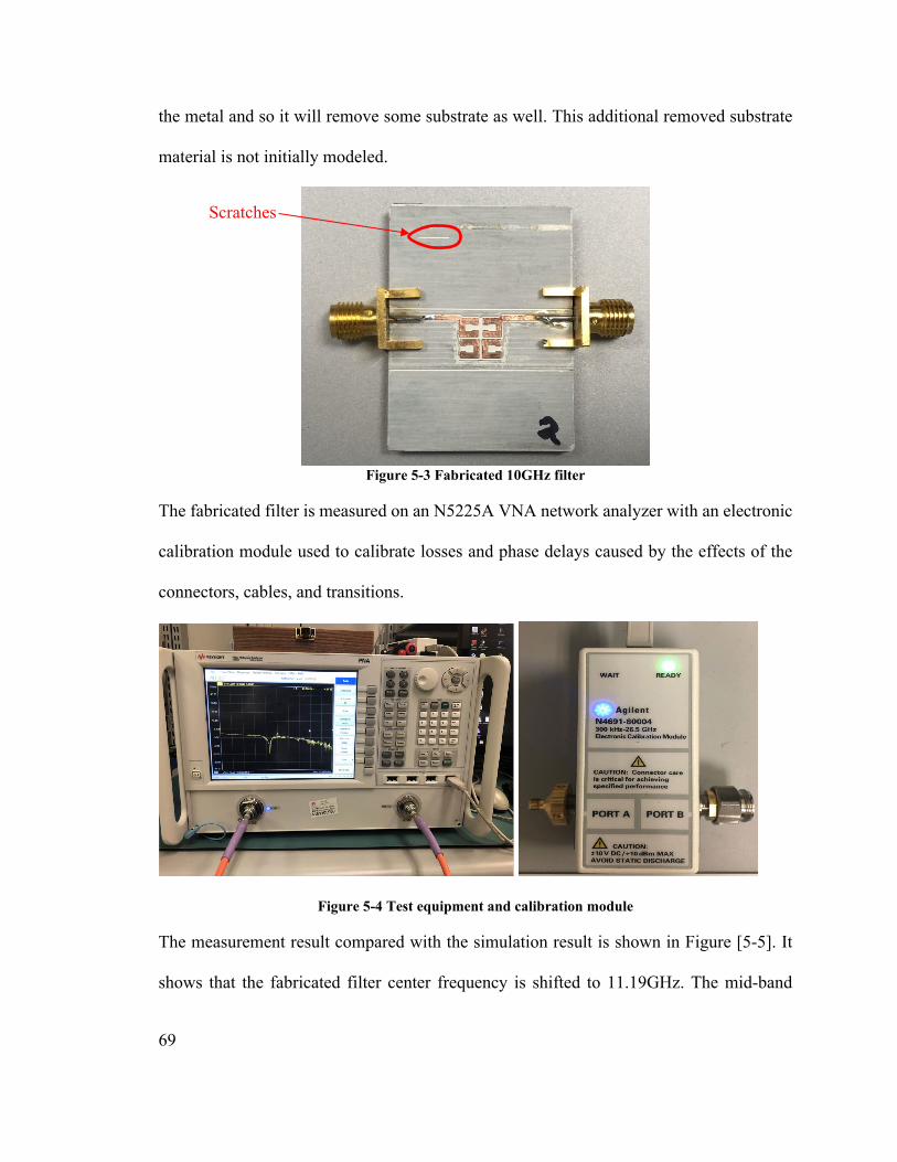
69
Scratches
the metal and so it will remove some substrate as well. This additional removed substrate
material is not initially modeled.
Figure 5-3 Fabricated 10GHz filter
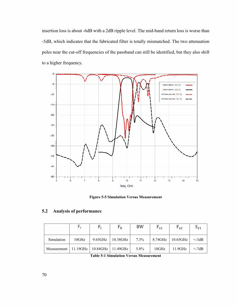
The fabricated filter is measured on an N5225A VNA network analyzer with an electronic
calibration module used to calibrate losses and phase delays caused by the effects of the
connectors, cables, and transitions.
Figure 5-4 Test equipment and calibration module
The measurement result compared with the simulation result is shown in Figure [5-5]. It
shows that the fabricated filter center frequency is shifted to 11.19GHz. The mid-band
70
insertion loss is about -6dB with a 2dB ripple level. The mid-band return loss is worse than
-5dB, which indicates that the fabricated filter is totally mismatched. The two attenuation
poles near the cut-off frequencies of the passband can still be identified, but they also shift
to a higher frequency.
Figure 5-5 Simulation Versus Measurement
5.2 Analysis of performance
Fc Fl Fh BW Fz1 Fz2 S21
Simulation 10GHz 9.65GHz 10.38GHz 7.3% 8.74GHz 10.65GHz <-3dB
Measurement 11.19GHz 10.84GHz 11.49GHz 5.8% 10GHz 11.9GHz <-7dB
Table 5-1 Simulation Versus Measurement
71
Table [5-1] summarizes the measurement result and the simulation result. Actual test
results and simulation results show substantial discrepancies. The possible explanation is
due to the milling depth of the fabrication machine.
As mentioned above in Figure [5-2], the milling depth of the machine must be adjusted
manually, and this will change the resonator’s frequency. In Figure [5-6], an HFSS model
is created trying to model the effect of this milling depth. A cavity around the filter structure
is created to simulate the relation between different milling depth and the filter’s frequency
response. The simulation results are shown in Figure [5-7] and Figure [5-8].
Figure 5-6 Modelling edge effect in HFSS
72
Figure 5-7 S11 for milling depth from 0.1mm to 0.3mm
Figure 5-8 S21 for milling depth from 0.1mm to 0.3mm
From the figure shown above, as the milling depth becomes deeper, the return loss gets
worse, and the center frequency moves toward a higher frequency.
For a more accurate analysis, the actual milling depth of the fabricated filter is measured
by a 3D optical profilometer. Figure [5-9] is the measurement result. The milling depth is
the distance between the substrate and the cutting edge, which is 0.243mm in the figure.
The tapped line width is also measured and is shown in Figure [5-10]. The actual width is
0.743mm, which is close to 0.75mm in the original simulation.
73
Figure 5-9 Measuring the milling depth of the fabricated filter
Figure 5-10 Measurement of conductor width
Adding a 0.243mm milling depth into the simulation, the comparison of the simulation
result and the real measurement result is in Figure [5-11]. The results show consistency.
74
Figure 5-11 Filter with 0.243mm milling depth simulation result compare with the measurement
result
This proves our theory that the milling depth is the main reason for the frequency shift and
impedance mismatch observed during measurement. If the filter would have been
implemented in a standard PCB fabrication process, we have reason to believe the
measurement result will show consistency with the original simulation result.
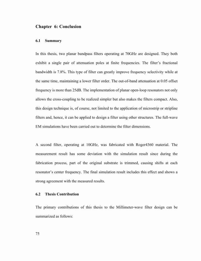
75
Chapter 6: Conclusion
6.1 Summary
In this thesis, two planar bandpass filters operating at 70GHz are designed. They both
exhibit a single pair of attenuation poles at finite frequencies. The filter’s fractional
bandwidth is 7.8%. This type of filter can greatly improve frequency selectivity while at
the same time, maintaining a lower filter order. The out-of-band attenuation at 0.05 offset
frequency is more than 25dB. The implementation of planar open-loop resonators not only
allows the cross-coupling to be realized simpler but also makes the filters compact. Also,
this design technique is, of course, not limited to the application of microstrip or stripline
filters and, hence, it can be applied to design a filter using other structures. The full-wave
EM simulations have been carried out to determine the filter dimensions.
A second filter, operating at 10GHz, was fabricated with Roger4360 material. The
measurement result has some deviation with the simulation result since during the
fabrication process, part of the original substrate is trimmed, causing shifts at each
resonator’s center frequency. The final simulation result includes this effect and shows a
strong agreement with the measured results.
6.2 Thesis Contribution
The primary contributions of this thesis to the Millimeter-wave filter design can be
summarized as follows:
76
Presented a novel vertical coupling structure of the six-order filter indicates
that multilayer technology can be applied to overcome the fabrication limit on
the planar filter. By putting two resonators on two different layers in an LTCC
module, the required distance to get the coupling coefficient can be achieved
with no horizontal limitation.
The design and fabrication of a 10GHz filter which uses Rogers material have
been presented. The measurement result is not matched with the simulation
result since the thickness of the substrate has been trimmed during the
fabrication process. Simulation result with the trimmed substrate is in strong
agreement with the measurement result.
Experimental validation indicates that the planar filter in an LTCC module can
be achieved at E-band frequency. The insertion loss is normally around 4-5dB,
which is mainly due to conductor loss. The thickness of the substrate will
influence filter performance and need to be treated carefully.
6.3 Future work
There are several areas left for future improvement. First, the conductor loss of the planar
filter can be reduced by the substitution of substrate integrated waveguide (SIW).[25] The
conductor loss would increase as the frequency goes higher. At E-band frequency, the
dissipation loss through a conductor is much higher compared with dielectric loss. By
substituting conductor to SIW, there will be no surface current, and this would largely
decrease the insertion loss.
77
Another improvement is to design a cascade of the filter in Figure [4-1]. Each fourth-order
filter can be considered as a basic unit. By cascading each of them one by one, several out-
of-band transmission zeros could be achieved to further improve the filter selectivity.
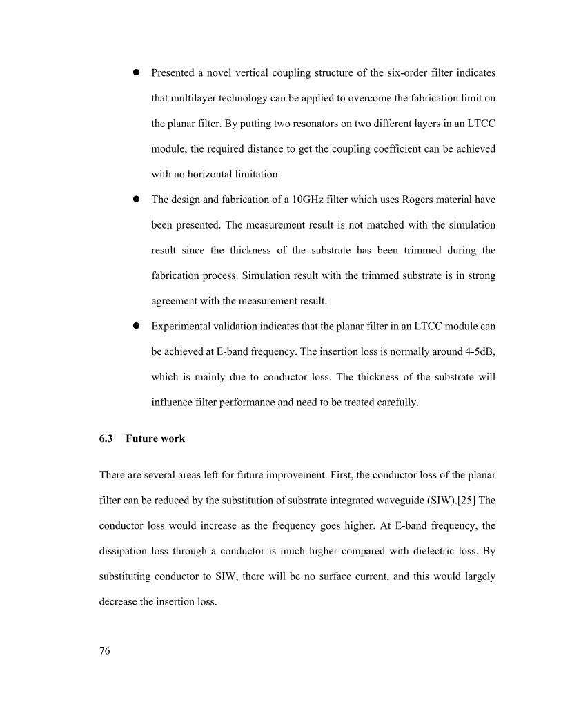
Figure 6-1 cascade of two fourth-order filters Figure [6-1] is a cascade structure of two four-order filters. Two pair of transmission zeros
could be achieved. Figure [6-2] is the frequency response of this filter. Two pair of
transmission zeros next to the passband could further improve the filter selectivity. The
disadvantage of this structure is that the conductor loss would increase due to the higher
filter order.
Figure 6-2 Frequency response of the filter with two pair of transmission zero
78
Reference
[1] “Cisco visual networking index (VNI) global mobile data traffic,” white Pap.
Cisco.com, 2014.
[2] J. G. Andrews et al., “What will 5G be?” IEEE J. Sel. Areas Commun., vol. 32, no.
6, pp. 1065–1082, 2014.
[3] W. Roh et al., “Millimeter-Wave Beamforming As An Enabling Technology For 5g
Cellular Communications: Theoretical feasibility and prototype results,” IEEE
Commun. Mag., vol. 52, no. 2, pp. 106–113, 2014.
[4] D. M. Pozar, Microwave Engineering, 4th ed. 2012.
[5] Z. Qingling and J. Li, “Rain Attenuation in Millimeter Wave Ranges,” IEEE, 2007.
[6] S. Rangan, T. S. Rappaport, and E. Erkip, “Millimeter-Wave Cellular Wireless
Networks: Potentials And Challenges,” Proc. IEEE, vol. 102, no. 3, pp. 366–385,
2014.
[7] F. Gutierrez and S. M. Ieee, “State of the Art in 60-GHz Integrated Circuits and
Systems for Wireless Communications,” Proc. IEEE (Volume99 , Issue 8 ), vol. 99,
no. 8, 2015.
[8] V. Miraftab, W. Zhai, and M. Repeta, “A Wideband Low-Cost E-Band Siw Antenna
Array For High Capacity Mmwave Radio,” 2015 IEEE MTT-S Int. Microw. Symp.
IMS, 2015, pp. 1–3, 2015.
[9] W. Zhai, M. Repeta, D. Wessel, and W. Tong, “Mm-Wave Large-Scale Phased
Array Based On Randomly Tiled Rectangular Sub-Arrays For 5G Communications,”
IEEE MTT-S Int. Microw. Symp. Dig., pp. 1895–1898, 2017.
79
[10] K. Nishikawa, T. Seki, I. Toyoda, and S. Kubota, “Compact 60-GHz LTCC Stripline
Parallel-Coupled Bandpass Filter With Parasitic Elements For Millimeter-Wave
System-On-Package.” in IEEE MTT-S International Microwave Symposium Digest,
2007.
[11] Geroge. L. Matthaei, l. Young, and e. M. T. Jones, Microwave Filters, Impedance-
Matching Networks, and Coupling Structures. 2000.
[12] J. S. Hong and M. J. Lancaster, “Design of Highly Selective Microstrip Bandpass
Filters with a Single Pair of Attenuation Poles at Finite Frequencies,” IEEE Trans.
Microw. Theory Tech., vol. 48, no. 7 PART 1, pp. 1098–1107, 2000.
[13] R. Levy, “Filters with Single Transmission Zeros at Real or Imaginary Frequencies,”
IEEE Trans. Microw. Theory Tech., vol. 24, no. 4, pp. 172–181, 1976.
[14] K. T. Jokela, “Narrow-band Stripline or Microstrip Filters with Transmission Zeros
at Real and Imaginary Frequencies,” IEEE Trans. Microw. Theory Tech., vol. M.
No. 6, pp. 542–547, 1980.
[15] Jia-sheng Hong, Microstrip Filters for RF/Microwave Applications.
[16] R. Levy and S. B. Cohn, “A History of Microwave Filter Research, Design, and
Development,” IEEE Trans. Microw. Theory Tech., vol. 32, no. 9, pp. 1055–1067,
1984.
[17] M. J. Lancaster and J. S. Hong, “Realisation of quasielliptic function filter using
dual-mode microstrip square loop resonators,” Electron. Lett., vol. 31, no. 24, pp.
2085–2086, 2002.
80
[18] S. J. Yao, R. R. Bonetti, and A. E. Williams, “Generalized Dual-Plane Multicoupled
Line Filters,” IEEE Trans. Microw. Theory Tech., vol. 41, no. 12, pp. 2182–2189,
1993.
[19] Rony. E. Amaya, A. Momciu, and I. Haroun, “High-performance, compact quasi-
elliptic bandpass filters for V-band high data rate radios,” IEEE Trans. Components,
Package. Manuf. Technol., vol. 3, no. 3, pp. 411–416, 2013.
[20] J.-S. Hong and M. J. Lancaster, “Coupling of Microstrip Open-Loop Resonators for
Cross-Coupled Planar Microwave Filters,” Ieee Trans. Microw. Theory Tech., vol.
44, no. 12, pp. 2099–2109, 1996.
[21] Advanced Design System: ADS2009U1-Momentum, Agilent Technologies, Santa
Clara, Ca, 2009
[22] S. J. Hedges, W. H. Road, G. Baddow, R. G. Humphreys, E. Division, and G.
Malvern, “An Extracted Pole Microstrip Elliptic Function Filter Using High-
Temperature Superconductors” in 24th European Microwave Conference, 1994, vol.
189, no. 1986, pp. 517–521.
[23] G. L. Matthaei and G. L. Hey-Shipton, “Novel Staggered Resonator Array
Superconducting 2.3-GHz Bandpass Filter,” IEEE Trans. Microw. Theory Tech., vol.
41, no. 12, pp. 2345–2352, 1993.
[24] LPKF: Manual ProtoMat S100, LPKF Laser & Electronics AG, 2006
[25] T. Martin, A. Ghiotto, F. Lotz, and T. P. Vuong, “Air-Filled SIW Filters for K-to E-
Band Substrate Integrated Systems,” 2018 IEEE MTT-S Int. Conf. Numer.
Electromagn. Multiphysics Model. Optim. NEMO, 2018, no. 4, pp. 4–6, 2018.