Embed Size (px)
Citation preview

High-level State Machines & RTL Design
Prof. Usagi

• Clock -- Pulsing signal for enabling latches; ticks like a clock • The clock's period must be longer than the longest delay from the state register's output to
the state register's input, known as the critical path. • Synchronous circuit: sequential circuit with a clock • Clock period: time between pulse starts
• Above signal: period = 20 ns • Clock cycle: one such time interval
• Above signal shows 3.5 clock cycles • Clock duty cycle: time clock is high
• 50% in this case • Clock frequency: 1/period
• Above : freq = 1 / 20ns = 50MHz;
2
Recap: Clock signal
0ns 10ns 20ns 30ns 40ns 50ns 60ns 70ns 80ns 90ns
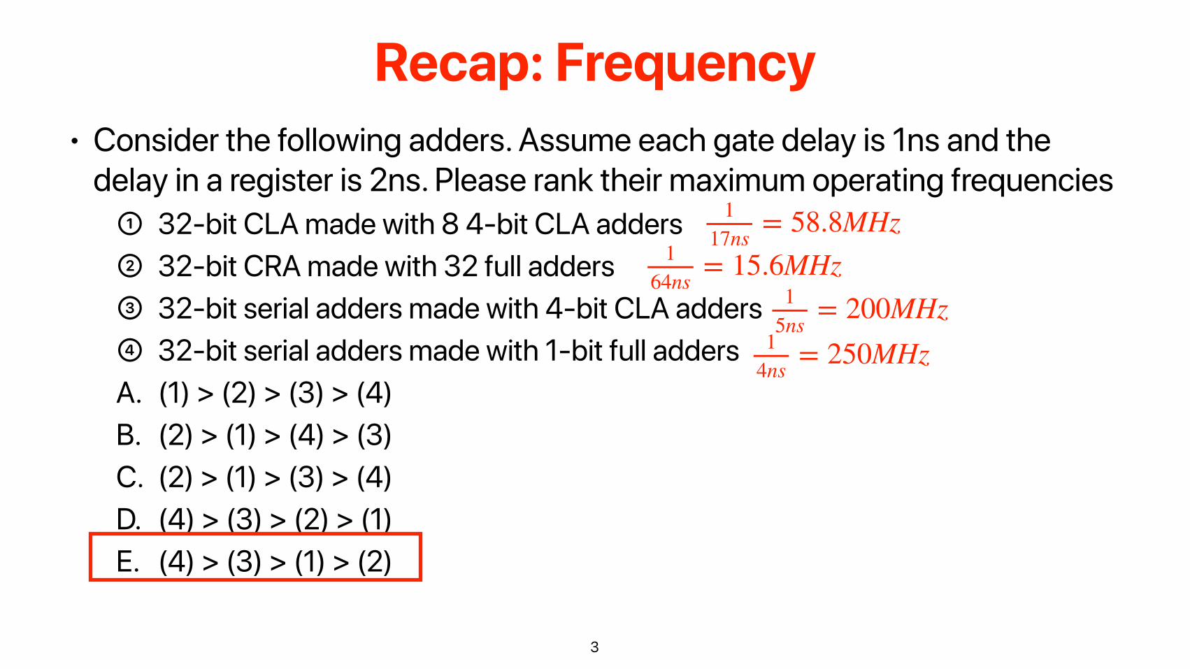
• Consider the following adders. Assume each gate delay is 1ns and the delay in a register is 2ns. Please rank their maximum operating frequencies ① 32-bit CLA made with 8 4-bit CLA adders ② 32-bit CRA made with 32 full adders ③ 32-bit serial adders made with 4-bit CLA adders ④ 32-bit serial adders made with 1-bit full adders A. (1) > (2) > (3) > (4) B. (2) > (1) > (4) > (3) C. (2) > (1) > (3) > (4) D. (4) > (3) > (2) > (1) E. (4) > (3) > (1) > (2)
3
Recap: Frequency
117ns = 58.8MHz
164ns
= 15.6MHz1
5ns= 200MHz
14ns = 250MHz

• Consider the following adders? ① 32-bit CLA made with 8 4-bit CLA adders ② 32-bit CRA made with 32 full adders ③ 32-bit serial adders made with 4-bit CLA adders ④ 32-bit serial adders made with 1-bit full adders A. Area: (1) > (2) > (3) > (4) Delay: (1) < (2) < (3) < (4) B. Area: (1) > (3) > (2) > (4) Delay: (1) < (3) < (2) < (4) C. Area: (1) > (3) > (4) > (2) Delay: (1) < (3) < (4) < (2) D. Area: (1) > (2) > (3) > (4) Delay: (1) < (3) < (2) < (4) E. Area: (1) > (3) > (2) > (4) Delay: (1) < (3) < (4) < (2)
4
Recap: Area/Delay of adders
Each CLA — 2-gate delay — 8*2+1 ~ 17Each carry — 2-gate delay — 64
Each CLA — (3-gate delay + 2-gate delay)*8 cycles — 5*8+1 = 41Each CLA — (2-gate delay + 2-gate delay)*32 cycles — 4*32 = 128
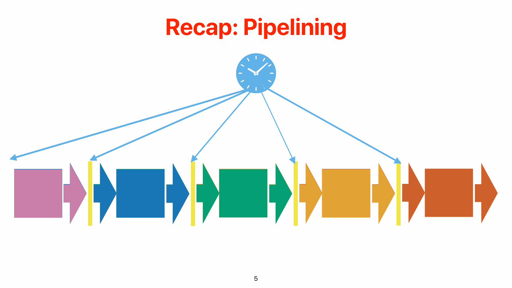
Recap: Pipelining
5
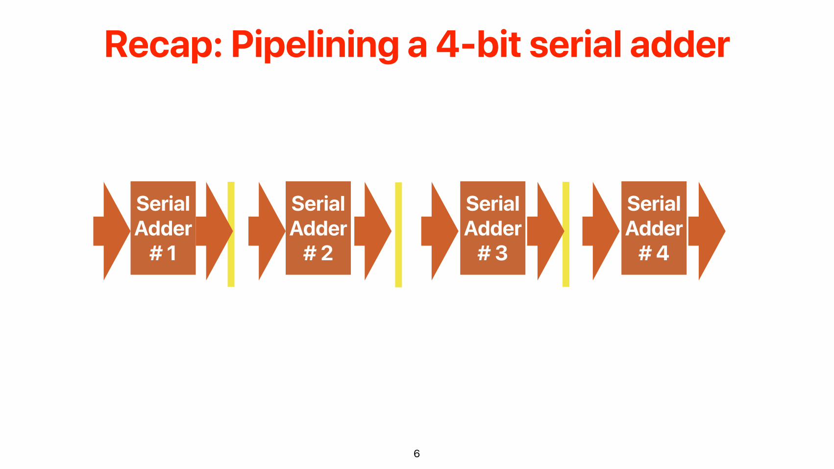
Recap: Pipelining a 4-bit serial adder
6
Serial Adder
# 1
Serial Adder
# 2
Serial Adder
# 3
Serial Adder
# 4

Recap: Pipelining a 4-bit serial adder
7
add a, b add c, d add e, f add g, h add i, j add k, l add m, n add o, p add q, r add s, t add u, v
1st 2nd 1st
3rd 2nd 1st
4th 3rd 2nd 1st
4th 3rd 2nd 1st
4th 3rd 2nd 1st
4th 3rd 2nd 1st
4th 3rd 2nd 1st
4th 3rd 2nd 1st
4th 3rd 2nd 1st
4th 3rd 2nd 1st
4th 3rd 4th 2nd 3rd 4th
t
After this point, we are completing an add operation each cycle!
CyclesAdd
= 1

Recap: Array style
8
b0
b1
b2
b3
a0 a1 a2 a3
5-bit adder
0 0
6-bit adder
00 0
0
7-bit adder
000
p7 p6 p5 p4 p3 p2 p1 p0

• What’s the estimated gate-delay of a 32-bit multiplier? (Assume adders are composed of 4-bit CLAs)
A. 0 — 100 B. 100 — 500 C. 500 — 1000 D. 1000 — 1500 E. > 1500
9
Recap: Gate-delays of 32-bit array-style multipliers
We need 33-64 bit adders33 - 36 -bit adders —> (9*2+1) gate delays *4
37 - 40 -bit adders —> (10*2+1) gate delays *441 - 44 -bit adders —> (11*2+1) gate delays *4
45 - 48 -bit adders —> (12*2+1) gate delays *449 - 52 -bit adders —> (13*2+1) gate delays *453 - 56 -bit adders —> (14*2+1) gate delays *457 - 60 -bit adders —> (15*2+1) gate delays *461 - 64 -bit adders —> (16*2+1) gate delays *4
4*2*(9+10+11+12+13+14+15+16+1) = 808
Each n-bit adder is roundup(n/4)*2+1
• More multipliers • HLSM • RTL Design • Designing a simple “microprocessor”
10
Outline
More on multipliers
11
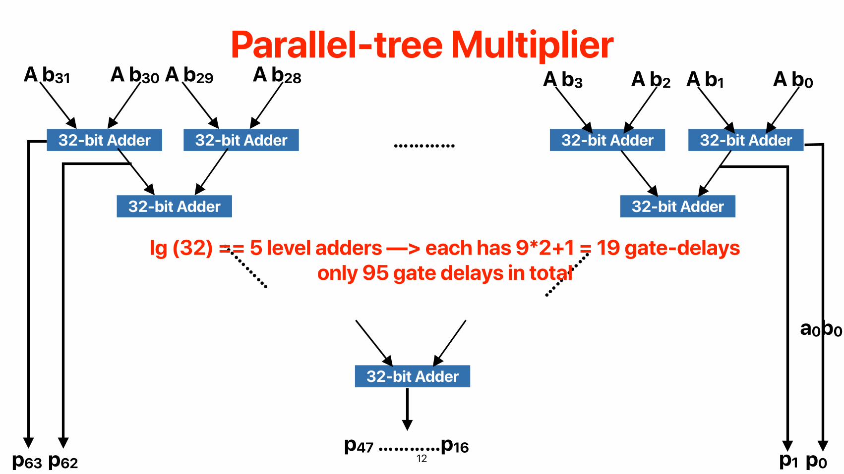
Parallel-tree Multiplier
12
32-bit Adder 32-bit Adder 32-bit Adder 32-bit Adder
32-bit Adder32-bit Adder
A b0
a0b0
p0
A b1
p1
A b2A b3A b28A b29A b30A b31
p63 p62
…………
32-bit Adder
……………………
p47 …………p16
lg (32) == 5 level adders —> each has 9*2+1 = 19 gate-delays only 95 gate delays in total

Sequential Logic based Multiplier!
13
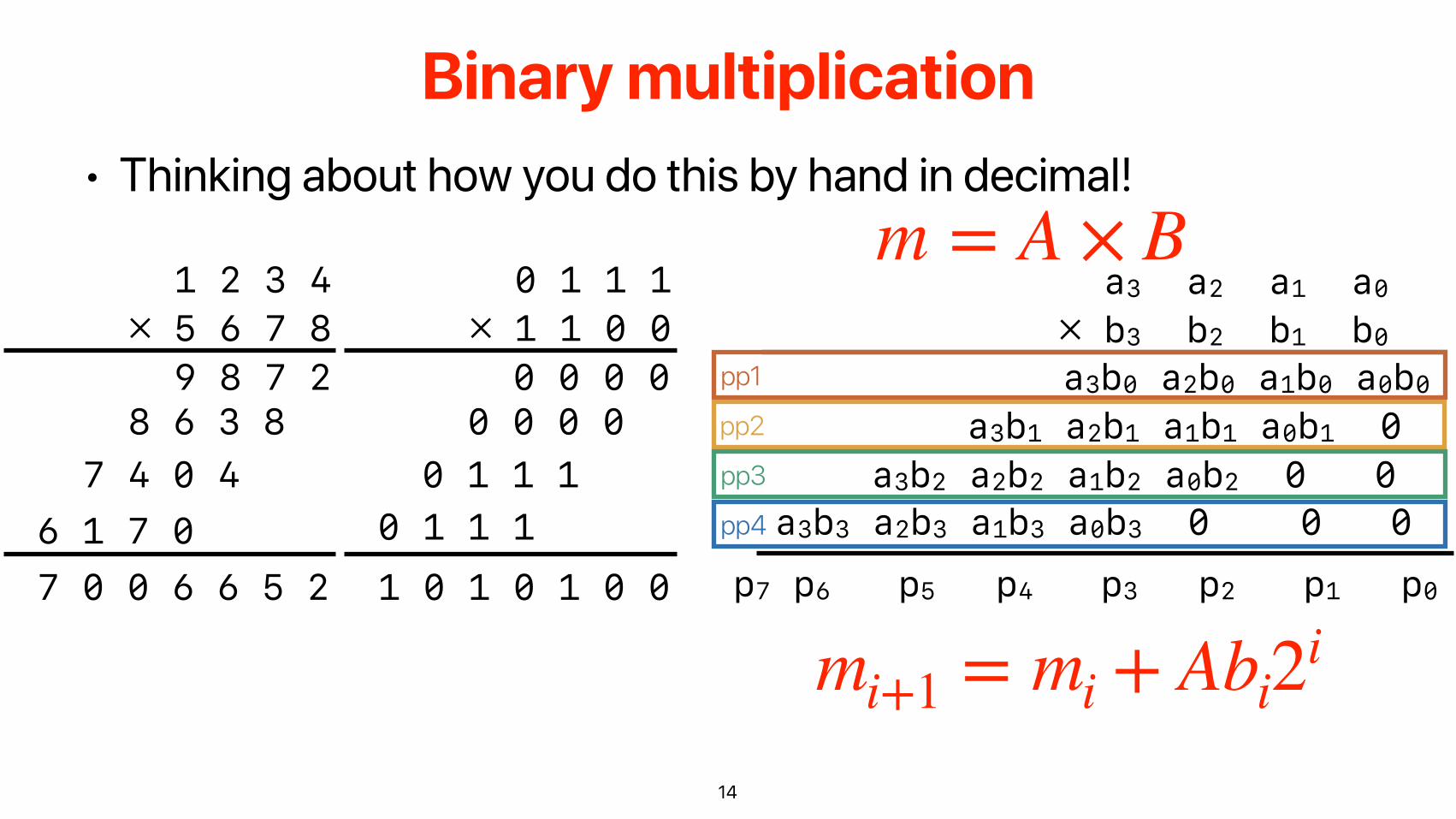
• Thinking about how you do this by hand in decimal!
14
Binary multiplication
1 2 3 4× 5 6 7 8
9 8 7 28 6 3 8
7 4 0 46 1 7 07 0 0 6 6 5 2
0 1 1 1× 1 1 0 00 0 0 0
0 0 0 00 1 1 1
0 1 1 11 0 1 0 1 0 0
a3 a2 a1 a0× b3 b2 b1 b0a3b0 a2b0 a1b0 a0b0
a3b1 a2b1 a1b1 a0b1 0a3b2 a2b2 a1b2 a0b2 0 0
a3b3 a2b3 a1b3 a0b3 0 0 0p7 p6 p5 p4 p3 p2 p1 p0
pp1
pp2
pp3
pp4
m = A × B
mi+1 = mi + Abi2i
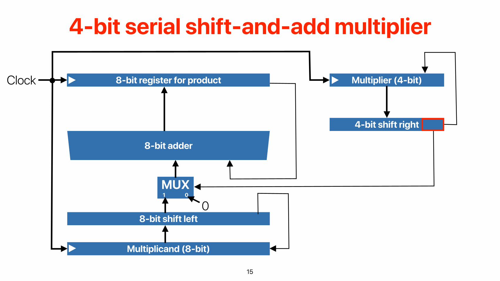
4-bit serial shift-and-add multiplier
15
8-bit register for product Multiplier (4-bit)
Multiplicand (8-bit)
MUX 1 0
8-bit adder
Clock
8-bit shift left
4-bit shift right
0

4-bit serial shift-and-add multiplier
16
8-bit register for product Multiplier (4-bit)
Multiplicand (8-bit)
MUX 1 0
8-bit adder
Clock
8-bit shift left
4-bit shift right
0
+5
+4
+2
+2
+2 +2
+4
— 13 gate delays
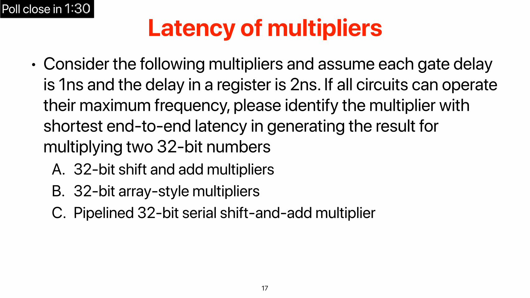
• Consider the following multipliers and assume each gate delay is 1ns and the delay in a register is 2ns. If all circuits can operate their maximum frequency, please identify the multiplier with shortest end-to-end latency in generating the result for multiplying two 32-bit numbers
A. 32-bit shift and add multipliers B. 32-bit array-style multipliers C. Pipelined 32-bit serial shift-and-add multiplier
17
Latency of multipliersPoll close in
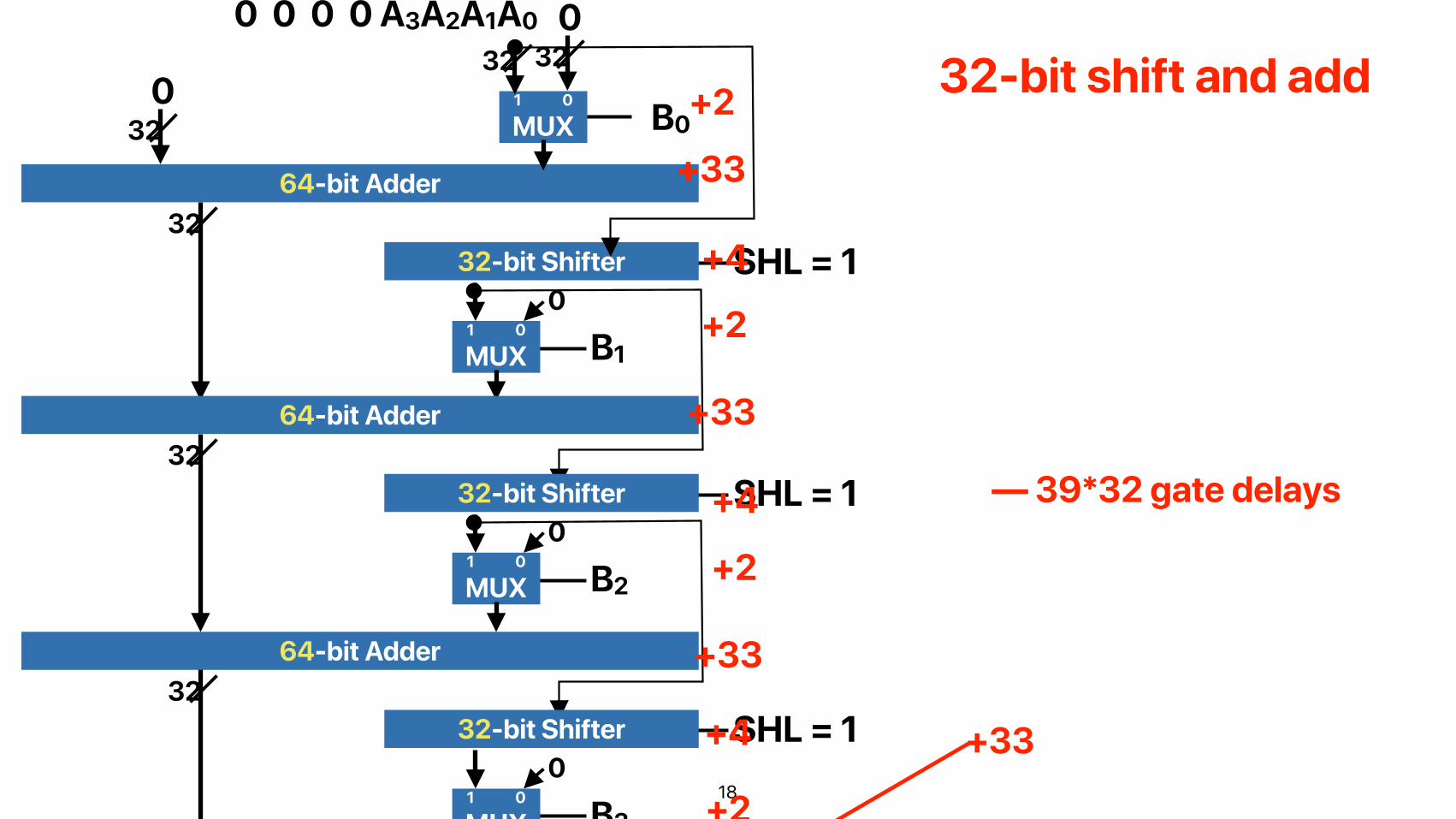
32-bit shift and add
18
B0
0 0 0 0 A3A2A1A0
32-bit Shifter SHL = 1
64-bit Adder
0 1 0
MUX32
320
32
32
1 0
MUX B1
0
64-bit Adder
32-bit Shifter SHL = 132
1 0
MUX B2
0
64-bit Adder
32-bit Shifter SHL = 132
1 0
MUX B3
0
+33
+2
+2
+4
+33
+2
+4
+33
+2
+4 +33
— 39*32 gate delays

• Which is the critical path of the multiplier?
19
32-bit serial shift-and-add multiplier
64-bit register for product Multiplier (32-bit)
Multiplicand (32-bit)
MUX 1 0
64-bit adder
Clock
32-bit shift left
32-bit shift right
0
AB C
D
E
Poll close in
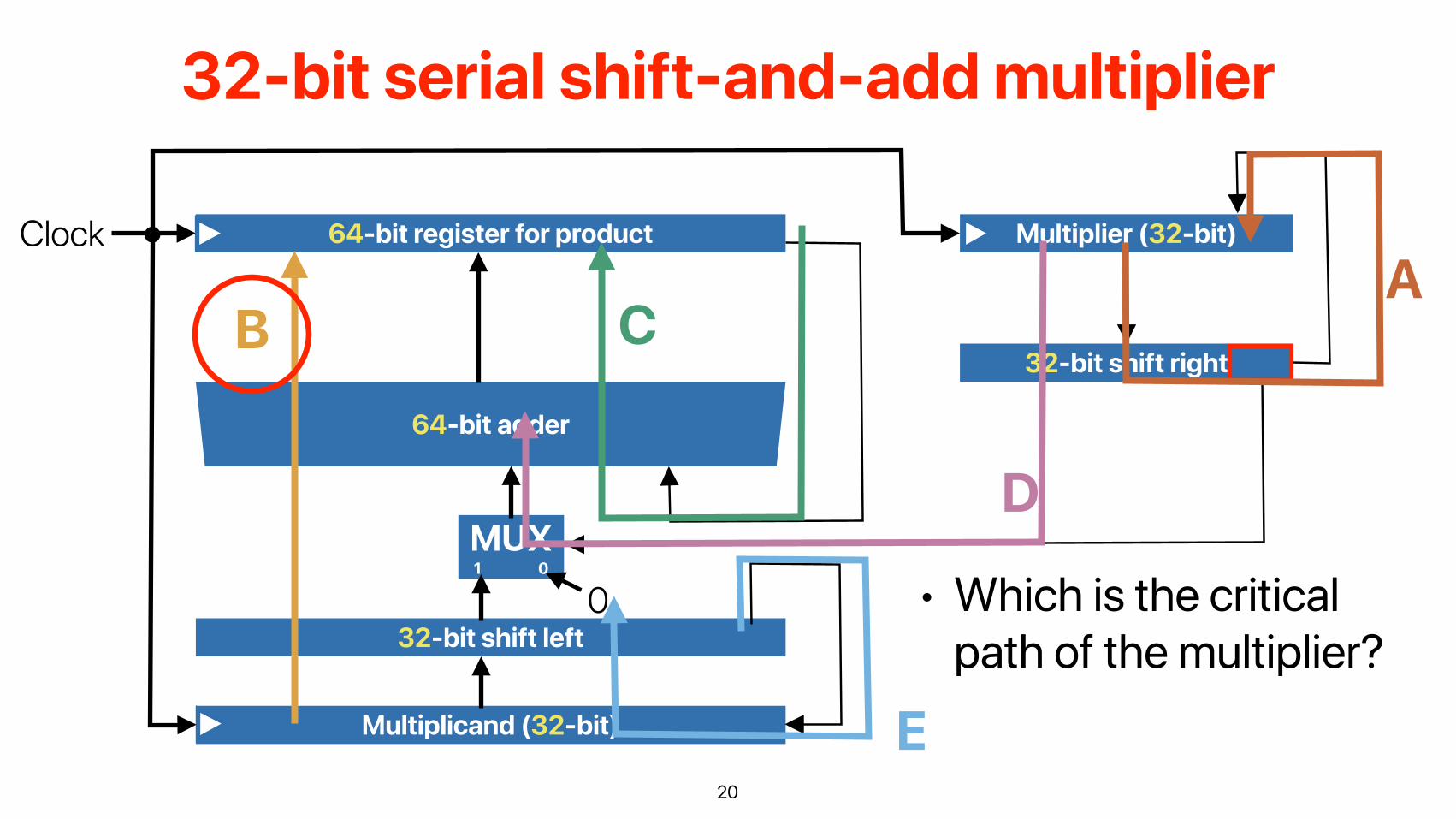
• Which is the critical path of the multiplier?
20
32-bit serial shift-and-add multiplier
64-bit register for product Multiplier (32-bit)
Multiplicand (32-bit)
MUX 1 0
64-bit adder
Clock
32-bit shift left
32-bit shift right
0
AB C
D
E

32-bit serial shift-and-add multiplier
21
64-bit register for product Multiplier (32-bit)
Multiplicand (32-bit)
MUX 1 0
64-bit adder
Clock
32-bit shift left
32-bit shift right
0
+33
+4
+2
+2
+2 +2
+4
— 41 gate delays
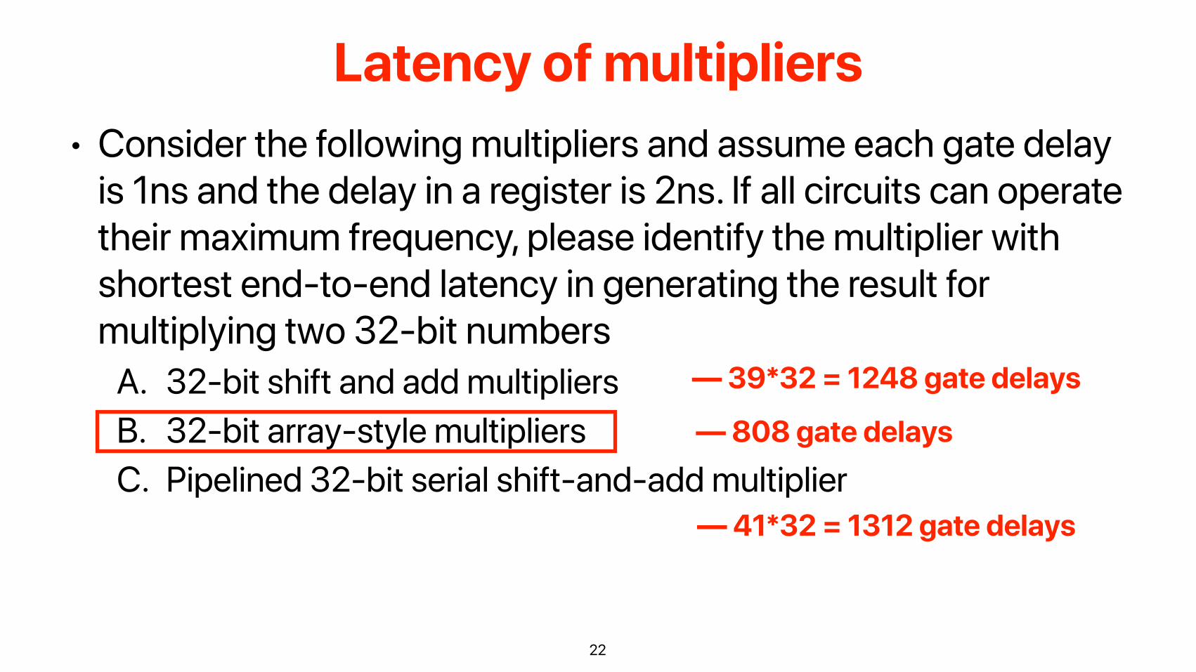
• Consider the following multipliers and assume each gate delay is 1ns and the delay in a register is 2ns. If all circuits can operate their maximum frequency, please identify the multiplier with shortest end-to-end latency in generating the result for multiplying two 32-bit numbers
A. 32-bit shift and add multipliers B. 32-bit array-style multipliers C. Pipelined 32-bit serial shift-and-add multiplier
22
Latency of multipliers
— 39*32 = 1248 gate delays
— 808 gate delays
— 41*32 = 1312 gate delays
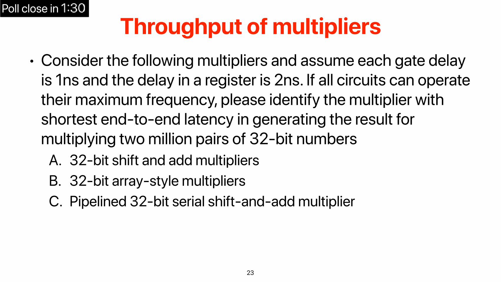
• Consider the following multipliers and assume each gate delay is 1ns and the delay in a register is 2ns. If all circuits can operate their maximum frequency, please identify the multiplier with shortest end-to-end latency in generating the result for multiplying two million pairs of 32-bit numbers
A. 32-bit shift and add multipliers B. 32-bit array-style multipliers C. Pipelined 32-bit serial shift-and-add multiplier
23
Throughput of multipliersPoll close in
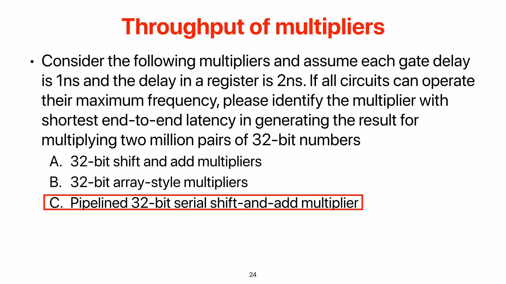
• Consider the following multipliers and assume each gate delay is 1ns and the delay in a register is 2ns. If all circuits can operate their maximum frequency, please identify the multiplier with shortest end-to-end latency in generating the result for multiplying two million pairs of 32-bit numbers
A. 32-bit shift and add multipliers B. 32-bit array-style multipliers C. Pipelined 32-bit serial shift-and-add multiplier
24
Throughput of multipliers

• We have learned all datapath components for an ALU! • Register • Shifter • Adders • Multiplier
• Processor has only one clock generator • Each datapath component has a different latency • We have make some of the above “serial” • How to control?
25
Let’s put all things together!
HLSM — High-Level State Machine
26

• Some behaviors may be too complex to describe by using classical FSMs
• Soda dispenser • c: bit input, 1 when coin deposited • a: 8-bit input: value of the
deposited coin • s: 8-bit input: cost of a soda • d: bit output, processor sets it to 1
when total value of deposited coins equals or exceeds cost of a soda
27
High-Level State Machine
Soda Dispenser
as
c
d
• How does the HLSM differ from the FSM for this problem? A. The HLSM stores multibit data, but the FSM doesn’t B. The FSM stores the state but the HLSM doesn’t C. Implementing HLSM and FSM requires multibit data registers D. All of the above E. None of the above
28
HLSMs v.s. FSMsPoll close in

• How does the HLSM differ from the FSM for this problem? A. The HLSM stores multibit data, but the FSM doesn’t B. The FSM stores the state but the HLSM doesn’t C. Implementing HLSM and FSM requires multibit data registers D. All of the above E. None of the above
29
HLSMs v.s. FSMs

• Which of the following are common between HLSMs and FSMs?
A. Transitions happen at the edge of a clock B. They both have external complex data C. All of the above D. None of the above
30
HLSMs v.s. FSMsPoll close in

• Which of the following are common between HLSMs and FSMs?
A. Transitions happen at the edge of a clock B. They both have external complex data C. All of the above D. None of the above
31
HLSMs v.s. FSMs

• High-level state machine (HLSM) extends FSM with:
• Multi-bit input/output • Local storage • Arithmetic operations
• Conventions • Each transition is implicitly ANDed with
a rising edge of the clock • Any bit output not explicitly assigned a
value in a state is implicitly assigned to 0. This convention does not apply for multibit outputs
• Every HLSM multibit output is registered
32
Benefits of HLSMs
Soda Dispenser
a (8-bit)s (8-bit)
c
d
Init WaitAdd
Disp.
c
tot:=tot+a
tot:=0d:=‘0’
c’*(tot<s) c’*(tot<s)’
d:=‘1’
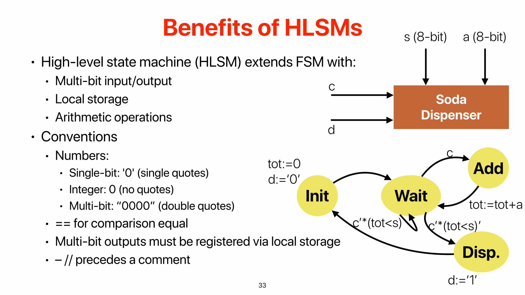
• High-level state machine (HLSM) extends FSM with: • Multi-bit input/output • Local storage • Arithmetic operations
• Conventions • Numbers:
• Single-bit: '0' (single quotes) • Integer: 0 (no quotes) • Multi-bit: “0000” (double quotes)
• == for comparison equal • Multi-bit outputs must be registered via local storage • – // precedes a comment
33
Benefits of HLSMs
Soda Dispenser
a (8-bit)s (8-bit)
c
d
Init WaitAdd
Disp.
c
tot:=tot+a
tot:=0d:=‘0’
c’*(tot<s) c’*(tot<s)’
d:=‘1’
RTL(Register Transfer Level) Design
34
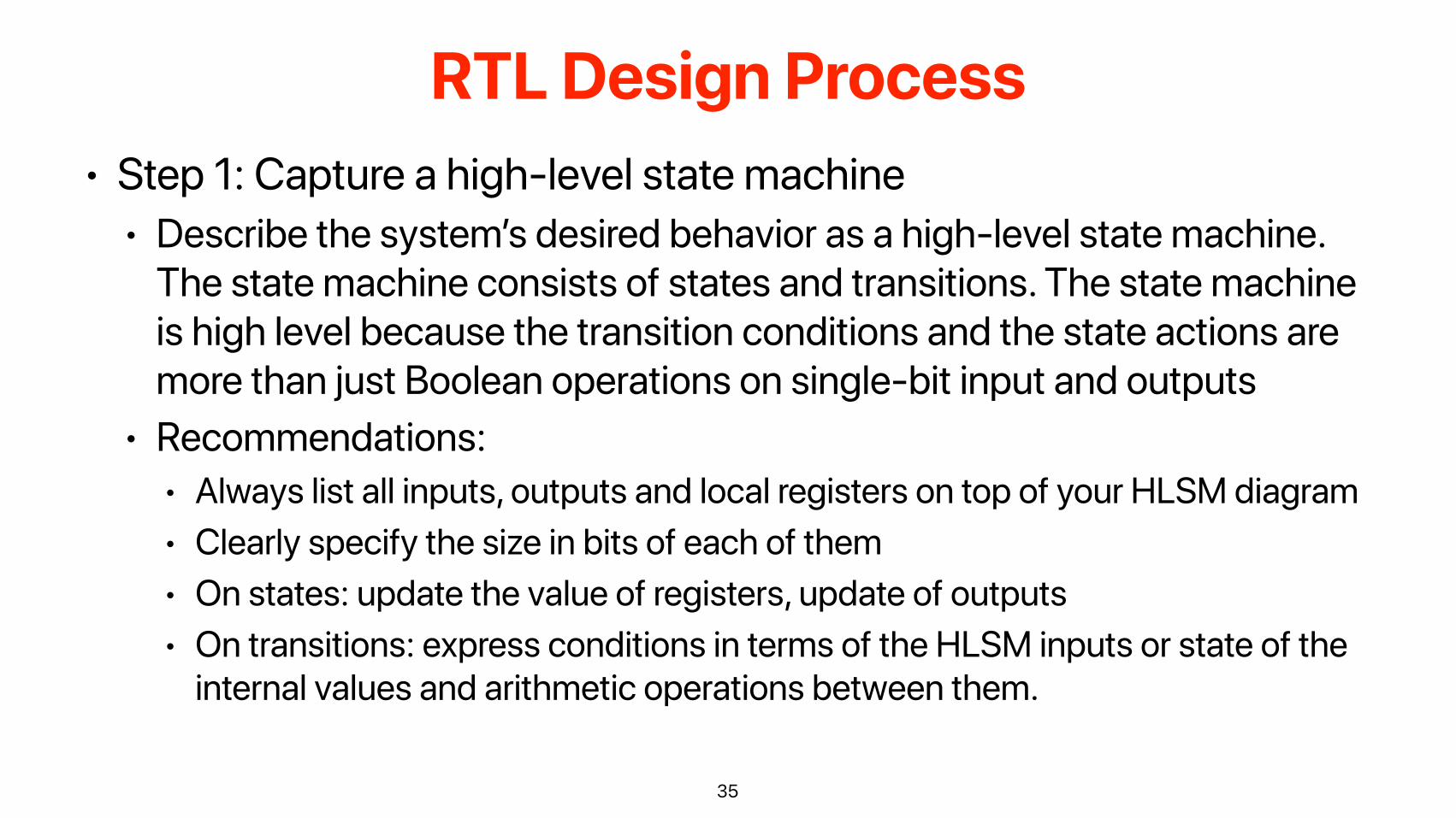
• Step 1: Capture a high-level state machine • Describe the system’s desired behavior as a high-level state machine.
The state machine consists of states and transitions. The state machine is high level because the transition conditions and the state actions are more than just Boolean operations on single-bit input and outputs
• Recommendations: • Always list all inputs, outputs and local registers on top of your HLSM diagram • Clearly specify the size in bits of each of them • On states: update the value of registers, update of outputs • On transitions: express conditions in terms of the HLSM inputs or state of the
internal values and arithmetic operations between them.
35
RTL Design Process
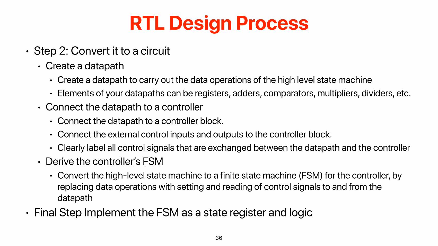
• Step 2: Convert it to a circuit • Create a datapath
• Create a datapath to carry out the data operations of the high level state machine • Elements of your datapaths can be registers, adders, comparators, multipliers, dividers, etc.
• Connect the datapath to a controller • Connect the datapath to a controller block. • Connect the external control inputs and outputs to the controller block. • Clearly label all control signals that are exchanged between the datapath and the controller
• Derive the controller’s FSM • Convert the high-level state machine to a finite state machine (FSM) for the controller, by
replacing data operations with setting and reading of control signals to and from the datapath
• Final Step Implement the FSM as a state register and logic
36
RTL Design Process

• Capture the behavior with HLSM • Convertit to a circuit
• High-level architecture (datapath and control path) • Datapath capable of HLSM's data operations • Design controller to control the datapath
37
RTL Design Summary

• Register: tot • Comparator: to compare tot
and s • Adder: to update tot = tot + a • Connect datapath elements • I/O interface
38
Create Datapath for Soda Dispenser
Init WaitAdd
Disp.
c
tot:=tot+a
tot:=0d:=‘0’
c’*(tot<s) c’*(tot<s)’d:=‘1’
tot ldclr
8-bit <
8-bit adder
a
tot < s
s

• iEval — Capture your screenshot and you will receive a full credit assignment • Lab 6 is up — due on 6/2
• Watch the video and read the instruction BEFORE your session • There are links on both course webpage and iLearn lab section • Submit through iLearn > Labs
• Office Hours • All office hours share the same meeting instance — if you have registered once, you cannot do it
again. • Zoom does not resend registration confirmation and does not allow us to “re-approve” if you have
registered • The only way is to dig out the e-mail from Zoom
• Final exam will be held during the campus scheduled period to avoid conflicts • 6/11 11:30am — 2:59:59pm • About the same format as midterm, but longer • Will have a final review on 6/6 to help you prepare
39
Announcement

つづく
ElectricalComputerEngineering
Science 120A