Embed Size (px)
Citation preview
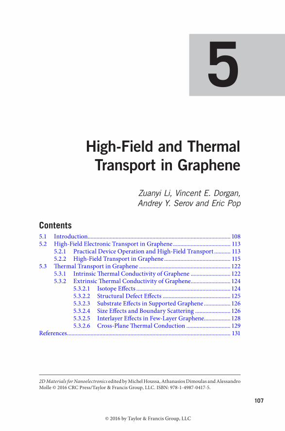
107
5High-Field and Thermal Transport in Graphene
Zuanyi Li, Vincent E. Dorgan, Andrey Y. Serov and Eric Pop
Contents5.1 Introduction................................................................................................. 1085.2 High-Field Electronic Transport in Graphene ....................................... 113
5.2.1 Practical Device Operation and High-Field Transport ........... 1135.2.2 High-Field Transport in Graphene ............................................. 115
5.3 Thermal Transport in Graphene .............................................................. 1225.3.1 Intrinsic Thermal Conductivity of Graphene ........................... 1225.3.2 Extrinsic Thermal Conductivity of Graphene ........................... 124
5.3.2.1 Isotope Effects ................................................................ 1245.3.2.2 Structural Defect Effects .............................................. 1255.3.2.3 Substrate Effects in Supported Graphene .................. 1265.3.2.4 Size Effects and Boundary Scattering ........................ 1265.3.2.5 Interlayer Effects in Few-Layer Graphene.................. 1285.3.2.6 Cross-Plane Thermal Conduction .............................. 129
References ............................................................................................................... 131
2D Materials for Nanoelectronics edited by Michel Houssa, Athanasios Dimoulas and Alessandro Molle © 2016 CRC Press/Taylor & Francis Group, LLC. ISBN: 978-1-4987-0417-5.
K24702_Book.indb 107 19-02-2016 14:26:25
© 2016 by Taylor & Francis Group, LLC
108
2D Materials for nanoelectronics
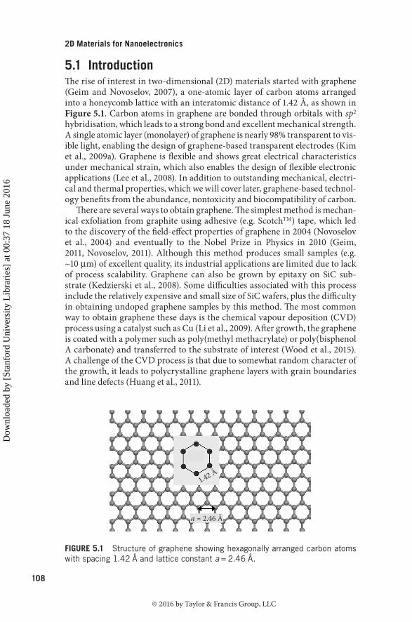
5.1 introductionThe rise of interest in two-dimensional (2D) materials started with graphene (Geim and Novoselov, 2007), a one-atomic layer of carbon atoms arranged into a honeycomb lattice with an interatomic distance of 1.42 Å, as shown in Figure 5.1. Carbon atoms in graphene are bonded through orbitals with sp2 hybridisation, which leads to a strong bond and excellent mechanical strength. A single atomic layer (monolayer) of graphene is nearly 98% transparent to vis-ible light, enabling the design of graphene-based transparent electrodes (Kim et al., 2009a). Graphene is flexible and shows great electrical characteristics under mechanical strain, which also enables the design of flexible electronic applications (Lee et al., 2008). In addition to outstanding mechanical, electri-cal and thermal properties, which we will cover later, graphene-based technol-ogy benefits from the abundance, nontoxicity and biocompatibility of carbon.
There are several ways to obtain graphene. The simplest method is mechan-ical exfoliation from graphite using adhesive (e.g. ScotchTM) tape, which led to the discovery of the field-effect properties of graphene in 2004 (Novoselov et al., 2004) and eventually to the Nobel Prize in Physics in 2010 (Geim, 2011, Novoselov, 2011). Although this method produces small samples (e.g. ~10 μm) of excellent quality, its industrial applications are limited due to lack of process scalability. Graphene can also be grown by epitaxy on SiC sub-strate (Kedzierski et al., 2008). Some difficulties associated with this process include the relatively expensive and small size of SiC wafers, plus the difficulty in obtaining undoped graphene samples by this method. The most common way to obtain graphene these days is the chemical vapour deposition (CVD) process using a catalyst such as Cu (Li et al., 2009). After growth, the graphene is coated with a polymer such as poly(methyl methacrylate) or poly(bisphenol A carbonate) and transferred to the substrate of interest (Wood et al., 2015). A challenge of the CVD process is that due to somewhat random character of the growth, it leads to polycrystalline graphene layers with grain boundaries and line defects (Huang et al., 2011).
a = 2.46 Å
1.42 Å
FiGUrE 5.1 Structure of graphene showing hexagonally arranged carbon atoms with spacing 1.42 Å and lattice constant a = 2.46 Å.
K24702_Book.indb 108 19-02-2016 14:26:25
© 2016 by Taylor & Francis Group, LLC
Dow
nloa
ded
by [
Stan
ford
Uni
vers
ity L
ibra
ries
] at
00:
37 1
8 Ju
ne 2
016
109
high-Field and thermal transport in Graphene
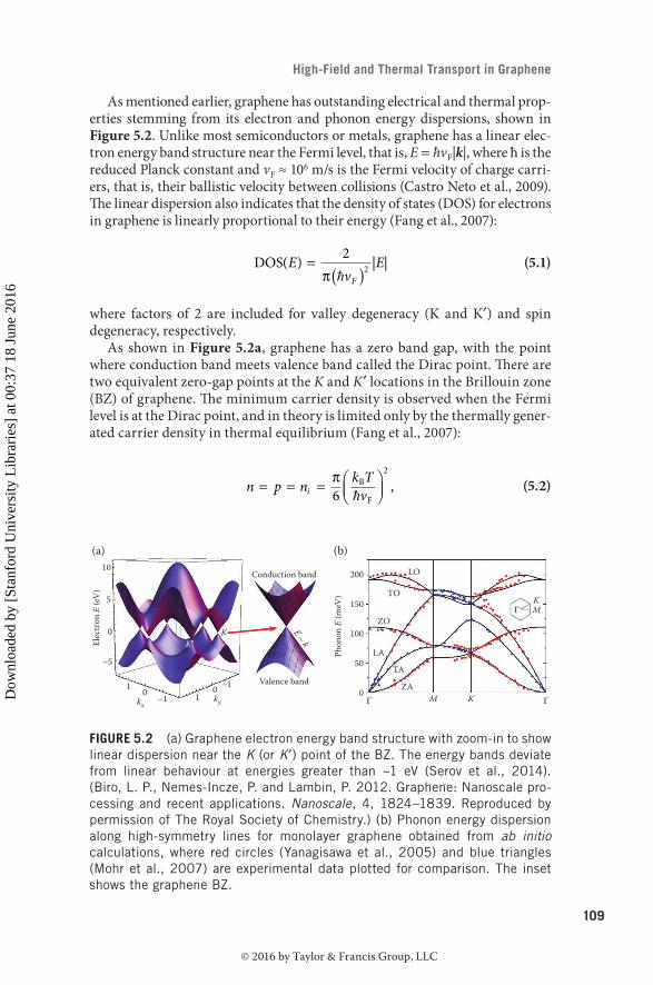
As mentioned earlier, graphene has outstanding electrical and thermal prop-erties stemming from its electron and phonon energy dispersions, shown in Figure 5.2. Unlike most semiconductors or metals, graphene has a linear elec-tron energy band structure near the Fermi level, that is, E = ħvF|k|, where ħ is the reduced Planck constant and vF ≈ 106 m/s is the Fermi velocity of charge carri-ers, that is, their ballistic velocity between collisions (Castro Neto et al., 2009). The linear dispersion also indicates that the density of states (DOS) for electrons in graphene is linearly proportional to their energy (Fang et al., 2007):
DOS | |( )E
vE
F
=( )
22π �
(5.1)
where factors of 2 are included for valley degeneracy (K and K′) and spin degeneracy, respectively.
As shown in Figure 5.2a, graphene has a zero band gap, with the point where conduction band meets valence band called the Dirac point. There are two equivalent zero-gap points at the K and K′ locations in the Brillouin zone (BZ) of graphene. The minimum carrier density is observed when the Fermi level is at the Dirac point, and in theory is limited only by the thermally gener-ated carrier density in thermal equilibrium (Fang et al., 2007):
n p n k T
vi= = =
π6
2B
F�,
(5.2)
200 LO
TO
ZO
LA
TA
ZA
KM
M K
150
100
50
Γ Γ
Γ
0
10Conduction band
Valence band
KK′
E ~ k
(a) (b)
0
Elec
tron
E (e
V)
5
Phon
on E
(meV
)
–5
1 –1010
kxky–1
FiGUrE 5.2 (a) Graphene electron energy band structure with zoom-in to show linear dispersion near the K (or K′) point of the BZ. The energy bands deviate from linear behaviour at energies greater than ~1 eV (Serov et al., 2014). (Biro, L. P., Nemes-Incze, P. and Lambin, P. 2012. Graphene: Nanoscale pro-cessing and recent applications. Nanoscale, 4, 1824–1839. Reproduced by permission of The Royal Society of Chemistry.) (b) Phonon energy dispersion along high-symmetry lines for monolayer graphene obtained from ab initio calculations, where red circles (Yanagisawa et al., 2005) and blue triangles (Mohr et al., 2007) are experimental data plotted for comparison. The inset shows the graphene BZ.
K24702_Book.indb 109 19-02-2016 14:26:27
© 2016 by Taylor & Francis Group, LLC
Dow
nloa
ded
by [
Stan
ford
Uni
vers
ity L
ibra
ries
] at
00:
37 1
8 Ju
ne 2
016
110
2D Materials for nanoelectronics
where kB is the Boltzmann constant and T is the temperature. However, in reality, various ionised impurities can induce local changes in the Dirac point, so-called ‘potential energy puddles’, which also increase the minimum carrier density (Zhang et al., 2009, Li et al., 2011a).
The fact that we cannot effectively decrease the carrier density means that graphene field-effect transistors (FETs) are difficult to switch off, mak-ing it challenging to utilise graphene for applications in digital electronics. Although a band gap can be introduced by quantum confinement, that is, pat-terning graphene into nanoribbons (GNRs), the GNR width corresponding to a reasonable band gap of ~0.5 eV is around just a few nanometers (Son et al., 2006, Han et al., 2007, Li et al., 2008, Huang et al., 2009), making the edges and associated edge roughness a significant part of the device. In reality, the mobility in narrow GNRs is typically lower than in pristine graphene even for 10–20-nm-wide devices (Jiao et al., 2009, Behnam et al., 2012). High mobility and good current density in large-scale graphene can be utilised in analogue applications and interconnects (Lin et al., 2010, Behnam et al., 2012, Wu et al., 2012), where off-state leakage is less important, while high on-current and transconductance (gain) are crucial. These applications as well as potential high-performance digital electronics require careful thermal management, where graphene can also play a role due to high thermal conductivity (k) (Balandin, 2011, Pop et al., 2012, Xu et al., 2014b).
The thermal properties of graphene can be better understood by inspect-ing the phonon dispersion, as shown in Figure 5.2b. Phonons, that is, the quantised lattice vibrations of single-layer graphene (SLG) have six branches corresponding to two atoms in the elementary cell: three acoustic modes (transverse TA, longitudinal LA and flexural ZA) and three optical modes (transverse TO, longitudinal LO and flexural ZO). Transverse and longitudi-nal acoustic modes have high sound velocity vLA ≈ 21 km/s and vTA ≈ 14 km/s (Pop et al., 2012), which leads to a strong contribution to thermal conductiv-ity. Flexural ZA and ZO modes correspond to out-of-plane vibrations. Unlike linear LA and TA modes, ZA has a quadratic dependence of frequency ω on wave vector q: ω ≈ αq2, which leads to the high DOS and big contribution to the thermal conductivity for suspended samples (Lindsay et al., 2010), which could exceed 2000 W/m/K at room temperature (Balandin, 2011, Pop et al., 2012, Xu et al., 2014b). For samples on a substrate (e.g. SiO2), ZA modes are suppressed by the interaction with the substrate (Seol et al., 2010, Ong and Pop, 2011), which leads to lower but still great thermal conductivity of sup-ported samples k ≈ 600 W/m/K (Seol et al., 2010). The thermal transport in graphene will be discussed in detail in Section 5.3.
Now, we first return to the electrical properties of graphene. Suspended samples with exfoliated graphene allow probing of intrinsic electrical prop-erties and exhibit charge carrier mobility as high as ~100,000 cm2/V/s albeit at low temperature (~5 K) and low carrier density n ~ 1010–1011 cm−2 (Bolotin et al., 2008). Such a high low-field mobility in suspended graphene can be explained by weak electron–phonon coupling, especially at lower carrier densities due to relatively high energy of optical phonons (ħωOP ≈ 200 meV) and intervalley acoustic phonons (ħωAC,i ≈ 140 meV) (Balandin, 2011,
K24702_Book.indb 110 19-02-2016 14:26:27
© 2016 by Taylor & Francis Group, LLC
Dow
nloa
ded
by [
Stan
ford
Uni
vers
ity L
ibra
ries
] at
00:
37 1
8 Ju
ne 2
016
111
high-Field and thermal transport in Graphene
Pop et al., 2012). As the energy of these phonons is much higher than kBT ≈ 26 meV at room temperature, the number of carriers which can emit these phonons is very low for equilibrium Fermi–Dirac distribution. On the other hand, the probability to absorb a high-energy phonon is limited by the nature of the Bose–Einstein distribution for phonons. The reasoning provided here is valid only in near-equilibrium conditions (low field), as it is much easier to emit optical phonons for non-equilibrium high-energy so-called ‘hot’ carriers (Serov et al., 2014).
Although suspended graphene devices exhibit outstanding electrical prop-erties, their utilisation for realistic electronics is very limited. First, the manu-facturing of suspended devices is a challenging process with low throughput (Bolotin et al., 2008, Dorgan et al., 2013). Second, it is difficult to modulate charge carrier density in suspended samples because of very weak capaci-tive coupling between graphene and the gate through the air or vacuum gap. Therefore, in order to make devices and circuits, graphene is most commonly placed on substrates compatible with conventional CMOS (complementary metal–oxide–semiconductor) processing, for example, Si/SiO2, Al2O3 or HfO2. However, when graphene is placed on a substrate, its electrical characteris-tics degrade quite significantly, with the low-field mobility typically less than 10,000 cm2/V/s. Such steep degradation of the low-filed mobility is related to various substrate-induced scattering mechanisms such as ionised impurity scattering and surface phonon scattering (Adam et al., 2009, Zhu et al., 2009, Perebeinos and Avouris, 2010, Ong and Fischetti, 2012c, Serov et al., 2014).
As graphene could be targeted towards interconnects and analogue appli-cations, the understanding of electrical transport at high electric fields can be beneficial for device analysis and optimisation. High-field transport in gra-phene has been studied both theoretically and experimentally. Experimental analysis is usually performed on a four-point structure or in multi-finger Hall configuration to exclude the effect of the contact resistance (Barreiro et al., 2009, DaSilva et al., 2010, Dorgan et al., 2010). It is usually observed that the current in graphene tends to saturate at higher electric field but does not reach ‘true’ saturation with output conductance gd = dId/dVd nearly zero (Barreiro et al., 2009, DaSilva et al., 2010, Dorgan et al., 2010). However, despite the lack of current saturation, it is possible to observe velocity saturation, albeit accompanied by the rising device temperature due to self-heating (Dorgan et al., 2010).
From the theoretical side, the velocity saturation in graphene is not an easy problem to solve, mostly due to the complicated nature of interaction of charge carriers in graphene with the substrate. The first theoretical studies of velocity saturation in graphene focussed on intrinsic graphene behaviour, therefore, mostly neglecting the substrate effect (Akturk and Goldsman, 2008, Shishir and Ferry, 2009). The tool of choice in this case is usually the Monte-Carlo method in momentum space, which naturally provides a simulation scheme for multiple scattering mechanisms (Jacoboni and Reggiani, 1983). The hydrodynamic model can also be used for modelling of high-field effects and has some advantages (Bistritzer and MacDonald, 2009, Svintsov et al., 2012, Serov et al., 2014).
K24702_Book.indb 111 19-02-2016 14:26:27
© 2016 by Taylor & Francis Group, LLC
Dow
nloa
ded
by [
Stan
ford
Uni
vers
ity L
ibra
ries
] at
00:
37 1
8 Ju
ne 2
016
112
2D Materials for nanoelectronics
Earlier theoretical studies on intrinsic graphene exhibit quite different results for velocity saturation: for example, one study demonstrated carrier-density-dependent saturation velocity vsat in the range between 0.3vF and 0.45vF using the ensemble Monte-Carlo method (Shishir and Ferry, 2009). Another study showed almost no carrier-density dependence in velocity satu-ration with much lower bound for vsat around 0.1vF (Bistritzer and MacDonald, 2009). The main difference between the two models lies in values for deforma-tion potentials for acoustic and optical phonons employed.
Later investigations (Li et al., 2010, 2011b, Perebeinos and Avouris, 2010), which incorporated the role of the substrate, pointed to the importance of interfacial substrate phonon modes and self-heating. However, the treatment of the substrate phonons was first performed with relatively simplistic models including no screening or static screening. A Monte-Carlo study involving substrate phonons (with static screening, but no substrate impurities) showed the velocity saturation between 0.4vF and 0.6vF (Li et al., 2010). The same group performed a similar study with self-heating taken into account and found carrier-density-dependent velocity saturation with vsat ranging between 0.15vF and 0.5vF (Li et al., 2011b). Similar results were shown using Monte-Carlo methods by another group, where substrate phonons were treated without screening yielding very high values for vsat between 0.4vF and 0.8vF depend-ing on the substrate material (between 0.4vF and 0.5vF for intrinsic graphene) (Perebeinos and Avouris, 2010). However, a recent detailed pseudo-potential-based Monte-Carlo study (with dynamic screening theory but without self-heating) pointed to lower numbers about 0.2vF to 0.3vF at room temperature (Fischetti et al., 2013). A more comprehensive study (Serov et al., 2014) using a hydrodynamic model considered self-heating and thermal coupling to the substrate, scattering with ionised impurities, graphene phonons, dynamically screened interfacial plasmon–phonon (IPP) modes and various substrates. It found that the high-field behaviour is determined by scattering with IPP modes and a small contribution of graphene phonons, and the drift velocity was benchmarked with available experimental data (Dorgan et al., 2010).
High-field effects in graphene are important not only in static (DC) regimes, but can also lead to a variety of interesting physical transient effects, especially at higher frequencies (Sekwao and Leburton, 2013). These effects render inter-esting features of electron–electron and electron–phonon interactions in zero band gap graphene. Up to this point, we have been discussing the charac-terisation of material properties of graphene usually performed experimen-tally in specialised test structures or in simulation with complicated methods such as the Monte Carlo or hydrodynamic model. A simpler characterisation usually involves a lumped compact model and basic extraction of transport coefficients such as mobility and contact resistance on a simple three- or four- terminal metal–oxide–semiconductor field-effect transistor (MOSFET) device. In order to bring together material properties and real device geom-etry, other methods such as the drift-diffusion model can be used to assist with device analysis. For instance, current saturation in graphene devices is an important topic because it is related to the analogue transistor gain, with better saturation resulting in higher gain (= gm/gd, where gm = ∂ID/∂VGS is the
K24702_Book.indb 112 19-02-2016 14:26:27
© 2016 by Taylor & Francis Group, LLC
Dow
nloa
ded
by [
Stan
ford
Uni
vers
ity L
ibra
ries
] at
00:
37 1
8 Ju
ne 2
016
113
high-Field and thermal transport in Graphene
transconductance and gd is the output conductance defined earlier). However, current saturation is not only caused by velocity saturation but also can be assisted electrostatically similar to the pinch-off effect in silicon MOSFETs, which can be captured by the Poisson equation in the drift-diffusion scheme. Other physical effects occurring alongside current saturation are band-to-band carrier generation and impact ionisation (Winzer et al., 2010, Girdhar and Leburton, 2011, Pirro et al., 2012). Despite the drift-diffusion method proving its merit for bulk semiconductors, relatively fewer efforts had assessed the applicability of drift-diffusion techniques to graphene (Ancona, 2010, Bae et al., 2011, Jimenez, 2011, Islam et al., 2013). In the next section, we will mainly discuss high-field electronic transport in graphene.
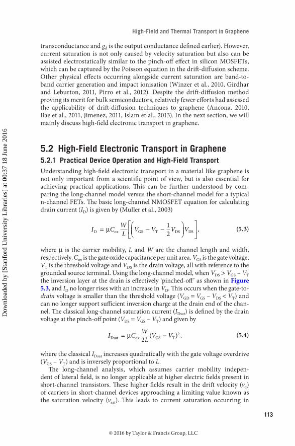
5.2 high-Field Electronic transport in Graphene5.2.1 Practical Device operation and high-Field transportUnderstanding high-field electronic transport in a material like graphene is not only important from a scientific point of view, but is also essential for achieving practical applications. This can be further understood by com-paring the long-channel model versus the short-channel model for a typical n-channel FETs. The basic long-channel NMOSFET equation for calculating drain current (ID) is given by (Muller et al., 2003)
I C W
LV V V VD ox GS T DS DS= − −
µ 1
2,
(5.3)
where μ is the carrier mobility, L and W are the channel length and width, respectively, Cox is the gate oxide capacitance per unit area, VGS is the gate voltage, VT is the threshold voltage and VDS is the drain voltage, all with reference to the grounded source terminal. Using the long-channel model, when VDS > VGS – VT the inversion layer at the drain is effectively ‘pinched-off’ as shown in Figure 5.3, and ID no longer rises with an increase in VD. This occurs when the gate-to-drain voltage is smaller than the threshold voltage (VGD = VGS – VDS < VT) and can no longer support sufficient inversion charge at the drain end of the chan-nel. The classical long-channel saturation current (IDsat) is defined by the drain voltage at the pinch-off point (VDS = VGS – VT) and given by
I C W
L V VDsat ox GS T= −µ 22( ) ,
(5.4)
where the classical IDsat increases quadratically with the gate voltage overdrive (VGS – VT) and is inversely proportional to L.
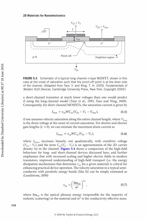
The long-channel analysis, which assumes carrier mobility indepen-dent of lateral field, is no longer applicable at higher electric fields present in short-channel transistors. These higher fields result in the drift velocity (vd) of carriers in short-channel devices approaching a limiting value known as the saturation velocity (vsat). This leads to current saturation occurring in
K24702_Book.indb 113 19-02-2016 14:26:29
© 2016 by Taylor & Francis Group, LLC
Dow
nloa
ded
by [
Stan
ford
Uni
vers
ity L
ibra
ries
] at
00:
37 1
8 Ju
ne 2
016
114
2D Materials for nanoelectronics
a short-channel transistor at much lower voltages than one would predict if using the long-channel model (Taur et al., 1993, Taur and Ning, 2009). Consequently, for short-channel MOSFETs, the saturation current is given by
I v WC V V VDsat sat ox GS T Dsat≈ − −( ), (5.5)
if one assumes velocity saturation along the entire channel length, where VDsat is the drain voltage at the onset of current saturation. For shorter and shorter gate lengths (L → 0), we can estimate the maximum drain current as
I v WC V VDmax sat ox GS T= −( ), (5.6)
where IDmax increases linearly, not quadratically, with overdrive voltage (VGS – VT) and the term Cox(VG – VT) is an approximation of the 2D carrier density (n) in the channel. Figure 5.4 shows a comparison of the high-field behaviour for long- and short-channel devices discussed here, and further emphasises that with increased scaling and higher electric fields in modern transistors, improved understanding of high-field transport (i.e. the energy dissipation mechanisms that determine vsat for a given material) is critical for enhancing practical device operation. The velocity saturation in a typical semi-conductor with parabolic energy bands (like Si) can be simply estimated as (Lundstrom, 2000)
v
msatOP≈
�ω*
/
,1 2
(5.7)
where ħωOP is the optical phonon energy (responsible for the majority of inelastic scattering) in the material and m* is the conductivity effective mass.
VGS > VT
VBS
VDS = VDsat
Depletion region
n+n+
p-Si Pinch-off
tOX
L
S DG
FiGUrE 5.3 Schematic of a typical long-channel n-type MOSFET, shown in this case at the onset of saturation such that the pinch-off point is at the drain side of the channel. (Adapted from Taur, Y. and Ning, T. H. 2009. Fundamentals of Modern VLSI Devices. Cambridge University Press, New York. Copyright 2009.)
K24702_Book.indb 114 19-02-2016 14:26:32
© 2016 by Taylor & Francis Group, LLC
Dow
nloa
ded
by [
Stan
ford
Uni
vers
ity L
ibra
ries
] at
00:
37 1
8 Ju
ne 2
016
115
high-Field and thermal transport in Graphene
vsat ≈ 107 cm/s in Si for both electrons and holes (Jacoboni et al., 1977). However, as we will see, this expression does not hold for graphene, where the energy bands near the Fermi level have a linear dispersion relationship.
Detailed knowledge of the coupling of high-field transport with self-heat-ing is also necessary when discussing practical device operation, since the ability to effectively remove heat from integrated circuits is a limiting factor for future scaling. At high fields, the charge carriers (e.g. electrons in conduc-tion band) accelerate and gain energy, or ‘heat up’. Mechanisms that may limit electron transport include electron scattering with other electrons, phonons, interfaces, defects and impurities. These scattering events not only determine vsat, but also when electrons scatter with phonons, electrons can lose energy to the lattice and effectively raise the temperature of the lattice (i.e. Joule heating or self-heating) (Pop et al., 2005, Pop and Goodson, 2006, Pop et al., 2006b). Consequently, it is important to account for self-heating effects when investi-gating high-field transport, as the electronic properties of a material may vary drastically with temperature. For example, the saturation velocity in Si shows a slight decrease with rising temperature due to an increase in phonon scat-tering (Jacoboni et al., 1977).
5.2.2 high-Field transport in GrapheneFor high-field transport in graphene, our discussion here is primarily con-cerned with monolayer graphene under steady-state transport. First, we focus on simulation results for ideal graphene and then include analysis of substrate effects and experimental data.
16
12
Long-channelbehaviour
VG = 2.5 Vto ∞
Without velocity saturationIDsat ∝ 1/L
IDmax = WCoxVsat(VG – VT)
With velocity saturation
Channel length LVDS (V)
VG = 2.5 V2.0 V1.5 V1.0 V0.5 V
0.25 μmNMOSFET
8
4
00
(a) (b)I D
S (m
A)
Satu
ratio
n dr
ain
curr
ent I
Dsa
t
1 2 3
FiGUrE 5.4 (a) Current–voltage characteristics for a Si NMOSFET with L = 0.25 μm and W = 9.5 μm. The solid lines are experimental curves, whereas the dashed line is the long-channel approximation with velocity saturation effects ignored. (Adapted from Taur, Y. et al. 1993. Solid-State Electron., 36, 1085–1087.) (b) Model predictions for MOSFET saturation current versus channel length without velocity saturation (dashed) and with velocity saturation (solid). (Adapted from Muller, R. S. et al. 2003. Device Electronics for Integrated Circuits. John Wiley & Sons, New York.)
K24702_Book.indb 115 19-02-2016 14:26:32
© 2016 by Taylor & Francis Group, LLC
Dow
nloa
ded
by [
Stan
ford
Uni
vers
ity L
ibra
ries
] at
00:
37 1
8 Ju
ne 2
016
116
2D Materials for nanoelectronics
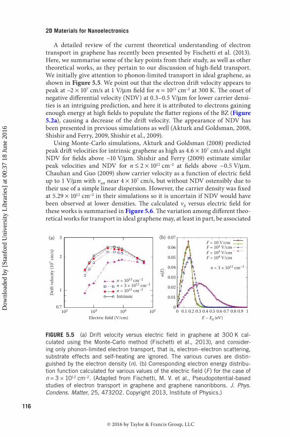
A detailed review of the current theoretical understanding of electron transport in graphene has recently been presented by Fischetti et al. (2013). Here, we summarise some of the key points from their study, as well as other theoretical works, as they pertain to our discussion of high-field transport. We initially give attention to phonon-limited transport in ideal graphene, as shown in Figure 5.5. We point out that the electron drift velocity appears to peak at ~2 × 107 cm/s at 1 V/μm field for n = 1013 cm−2 at 300 K. The onset of negative differential velocity (NDV) at 0.3–0.5 V/μm for lower carrier densi-ties is an intriguing prediction, and here it is attributed to electrons gaining enough energy at high fields to populate the flatter regions of the BZ (Figure 5.2a), causing a decrease of the drift velocity. The appearance of NDV has been presented in previous simulations as well (Akturk and Goldsman, 2008, Shishir and Ferry, 2009, Shishir et al., 2009).
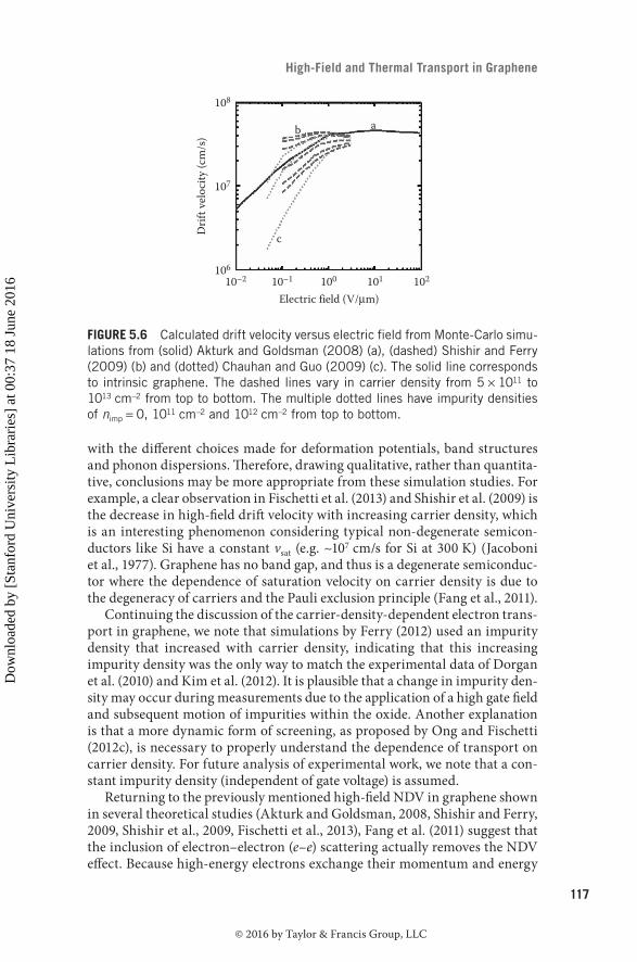
Using Monte-Carlo simulations, Akturk and Goldsman (2008) predicted peak drift velocities for intrinsic graphene as high as 4.6 × 107 cm/s and slight NDV for fields above ~10 V/μm. Shishir and Ferry (2009) estimate similar peak velocities and NDV for n ≤ 2 × 1012 cm−2 at fields above ~0.5 V/μm. Chauhan and Guo (2009) show carrier velocity as a function of electric field up to 1 V/μm with vsat near 4 × 107 cm/s, but without NDV ostensibly due to their use of a simple linear dispersion. However, the carrier density was fixed at 5.29 × 1012 cm−2 in their simulations so it is uncertain if NDV would have been observed at lower densities. The calculated vd versus electric field for these works is summarised in Figure 5.6. The variation among different theo-retical works for transport in ideal graphene may, at least in part, be associated
3 0.07
0.06
0.05
0.04
0.03
0.02
0.01
0
(a) (b)
2
1
0.7102 103
Electric field (V/cm)104
n = 1013 cm–2
n = 3 × 1012 cm–2
n = 3 × 1012 cm–2
F = 10 V/cmF = 102 V/cmF = 103 V/cmF = 104 V/cm
n = 1012 cm–2
Intrinsic
105 0 0.1 0.2 0.3 0.4 0.5E – E0 (eV)
0.6 0.7 0.8 0.9 1
Drif
t vel
ocity
(107 c
m/s
)
n(E)
FiGUrE 5.5 (a) Drift velocity versus electric field in graphene at 300 K cal-culated using the Monte-Carlo method (Fischetti et al., 2013), and consider-ing only phonon-limited electron transport, that is, electron–electron scattering, substrate effects and self-heating are ignored. The various curves are distin-guished by the electron density (n). (b) Corresponding electron energy distribu-tion function calculated for various values of the electric field (F) for the case of n = 3 × 1012 cm−2. (Adapted from Fischetti, M. V. et al., Pseudopotential-based studies of electron transport in graphene and graphene nanoribbons. J. Phys. Condens. Matter, 25, 473202. Copyright 2013, Institute of Physics.)
K24702_Book.indb 116 19-02-2016 14:26:32
© 2016 by Taylor & Francis Group, LLC
Dow
nloa
ded
by [
Stan
ford
Uni
vers
ity L
ibra
ries
] at
00:
37 1
8 Ju
ne 2
016
117
high-Field and thermal transport in Graphene
with the different choices made for deformation potentials, band structures and phonon dispersions. Therefore, drawing qualitative, rather than quantita-tive, conclusions may be more appropriate from these simulation studies. For example, a clear observation in Fischetti et al. (2013) and Shishir et al. (2009) is the decrease in high-field drift velocity with increasing carrier density, which is an interesting phenomenon considering typical non-degenerate semicon-ductors like Si have a constant vsat (e.g. ~107 cm/s for Si at 300 K) (Jacoboni et al., 1977). Graphene has no band gap, and thus is a degenerate semiconduc-tor where the dependence of saturation velocity on carrier density is due to the degeneracy of carriers and the Pauli exclusion principle (Fang et al., 2011).
Continuing the discussion of the carrier-density-dependent electron trans-port in graphene, we note that simulations by Ferry (2012) used an impurity density that increased with carrier density, indicating that this increasing impurity density was the only way to match the experimental data of Dorgan et al. (2010) and Kim et al. (2012). It is plausible that a change in impurity den-sity may occur during measurements due to the application of a high gate field and subsequent motion of impurities within the oxide. Another explanation is that a more dynamic form of screening, as proposed by Ong and Fischetti (2012c), is necessary to properly understand the dependence of transport on carrier density. For future analysis of experimental work, we note that a con-stant impurity density (independent of gate voltage) is assumed.
Returning to the previously mentioned high-field NDV in graphene shown in several theoretical studies (Akturk and Goldsman, 2008, Shishir and Ferry, 2009, Shishir et al., 2009, Fischetti et al., 2013), Fang et al. (2011) suggest that the inclusion of electron–electron (e–e) scattering actually removes the NDV effect. Because high-energy electrons exchange their momentum and energy
108
b a
c
Electric field (V/μm)
107
Drif
t vel
ocity
(cm
/s)
106
10–2 10–1 100 101 102
FiGUrE 5.6 Calculated drift velocity versus electric field from Monte-Carlo simu-lations from (solid) Akturk and Goldsman (2008) (a), (dashed) Shishir and Ferry (2009) (b) and (dotted) Chauhan and Guo (2009) (c). The solid line corresponds to intrinsic graphene. The dashed lines vary in carrier density from 5 × 10¹¹ to 1013 cm−2 from top to bottom. The multiple dotted lines have impurity densities of nimp = 0, 1011 cm−2 and 1012 cm−2 from top to bottom.
K24702_Book.indb 117 19-02-2016 14:26:32
© 2016 by Taylor & Francis Group, LLC
Dow
nloa
ded
by [
Stan
ford
Uni
vers
ity L
ibra
ries
] at
00:
37 1
8 Ju
ne 2
016
118
2D Materials for nanoelectronics
with low-energy electrons, e–e scattering weakens the backscattering effect that would lead to NDV (Fang et al., 2011). Another effect not yet discussed is carrier multiplication due to interband tunnelling and e–e scattering (Winzer et al., 2010, Girdhar and Leburton, 2011, Pirro et al., 2012). If the Fermi level is near the Dirac point, we could expect Zener tunnelling and/or impact ioni-sation to generate electrons and holes, especially at high fields, and increase the carrier concentration. Experimental studies have shown that it is very difficult to obtain saturation of high-field current in graphene transistors (Meric et al., 2008, Barreiro et al., 2009, DaSilva et al., 2010, Dorgan et al., 2010, Meric et al., 2011), a characteristic credited to the lack of a band gap in graphene, which facilitates ambipolar transport and the easy transition from electron- dominated to hole-dominated transport (or vice versa) during high-field operation.
We now turn to substrate effects, a necessary discussion in light of the fact that a majority of the experimental work on graphene has been performed with graphene on solid insulating substrates (e.g. SiO2/Si). An additional scattering process that limits electrical transport in supported graphene is scattering with charged impurities (Chen et al., 2008) and ‘remote’ substrate phonons (Serov et al., 2014). Substrate impurities that remain after the fabrication of graphene transistors (Martin et al., 2008, Deshpande et al., 2009, Zhang et al., 2009) play a significant role in limiting the low-field mobility of graphene transistors (Adam et al., 2007), but do not significantly affect high-field transport (Perebeinos and Avouris, 2010, Meric et al., 2011). In addition, we expect that if a graphene transistor is used in the future for nanoscale electronics, then it will most likely be a top- or multi-gated transistor with thin high-k insulator as the gate dielectric (Kim et al., 2009b, Zou et al., 2010). Detailed models have been provided for analysing the effect of charged impurity scattering and its dependence on the surrounding dielectric environment (Chen et al., 2009a, Ponomarenko et al. 2009, Ong and Fischetti, 2012a, 2013b), but as we are primarily con-cerned with high-field transport here, we will move on to a more relevant scattering process.
For insulators like SiO2 and HfO2, there are bulk dipoles associated with the ionicity of the metal–oxide bonds. These dipoles generate fringing fields on the substrate surface such that the frequencies of the dipoles are typically determined by the bulk LO phonons of the insulator. Electrons in close prox-imity to the substrate surface may interact with these surface optical (SO) phonons via a process commonly referred to as remote-phonon scattering. For Si inversion layers, remote-phonon scattering has been investigated (Hess and Vogl, 1979, Moore and Ferry, 1980), where it was found to have a small effect on the drift velocity in the regime just beyond Ohmic transport, but it was not strong enough to affect the saturation velocity (Leburton and Dorda, 1981), which is determined by the bulk Si optical phonons. In supported gra-phene, it is reasonable to consider electrons interacting strongly with SO pho-nons, considering electrons are essentially confined to the graphene sheet and the van der Waals gap between the graphene and substrate is small, ~0.3 nm (Ishigami et al., 2007). Furthermore, recent work shows that graphene may
K24702_Book.indb 118 19-02-2016 14:26:33
© 2016 by Taylor & Francis Group, LLC
Dow
nloa
ded
by [
Stan
ford
Uni
vers
ity L
ibra
ries
] at
00:
37 1
8 Ju
ne 2
016
119
high-Field and thermal transport in Graphene
even emit longitudinal out-of-plane acoustic phonons into the substrate, rep-resenting an energy dissipation mechanism in the vertical direction (Chen et al., 2014).
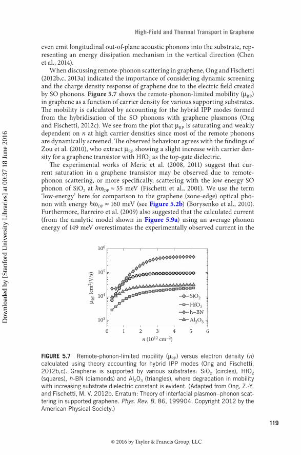
When discussing remote-phonon scattering in graphene, Ong and Fischetti (2012b,c, 2013a) indicated the importance of considering dynamic screening and the charge density response of graphene due to the electric field created by SO phonons. Figure 5.7 shows the remote-phonon-limited mobility (μRP) in graphene as a function of carrier density for various supporting substrates. The mobility is calculated by accounting for the hybrid IPP modes formed from the hybridisation of the SO phonons with graphene plasmons (Ong and Fischetti, 2012c). We see from the plot that μRP is saturating and weakly dependent on n at high carrier densities since most of the remote phonons are dynamically screened. The observed behaviour agrees with the findings of Zou et al. (2010), who extract μRP showing a slight increase with carrier den-sity for a graphene transistor with HfO2 as the top-gate dielectric.
The experimental works of Meric et al. (2008, 2011) suggest that cur-rent saturation in a graphene transistor may be observed due to remote-phonon scattering, or more specifically, scattering with the low-energy SO phonon of SiO2 at ħωOP ≈ 55 meV (Fischetti et al., 2001). We use the term ‘low-energy’ here for comparison to the graphene (zone-edge) optical pho-non with energy ħωOP ≈ 160 meV (see Figure 5.2b) (Borysenko et al., 2010). Furthermore, Barreiro et al. (2009) also suggested that the calculated current (from the analytic model shown in Figure 5.9a) using an average phonon energy of 149 meV overestimates the experimentally observed current in the
106
105
SiO2
HfO2h–BNAl2O3
104
103
0 1 2n (1012 cm–2)
μ RP (c
m2 /
V/s)
3 4 5 6
FiGUrE 5.7 Remote-phonon-limited mobility (μRP) versus electron density (n) calculated using theory accounting for hybrid IPP modes (Ong and Fischetti, 2012b,c). Graphene is supported by various substrates: SiO2 (circles), HfO2 (squares), h-BN (diamonds) and Al2O3 (triangles), where degradation in mobility with increasing substrate dielectric constant is evident. (Adapted from Ong, Z.-Y. and Fischetti, M. V. 2012b. Erratum: Theory of interfacial plasmon–phonon scat-tering in supported graphene. Phys. Rev. B, 86, 199904. Copyright 2012 by the American Physical Society.)
K24702_Book.indb 119 19-02-2016 14:26:33
© 2016 by Taylor & Francis Group, LLC
Dow
nloa
ded
by [
Stan
ford
Uni
vers
ity L
ibra
ries
] at
00:
37 1
8 Ju
ne 2
016
120
2D Materials for nanoelectronics
high-field limit. Unfortunately, these works do not account for self-heating effects in their analysis, which we know is evident in graphene transistors at high currents and high fields (Chae et al., 2009, Freitag et al. 2009, Bae et al., 2010, 2011, Berciaud et al., 2010) and appears necessary to explain high-field transport in graphene (DaSilva et al., 2010, Perebeinos and Avouris, 2010, Li et al., 2011b, Islam et al., 2013).
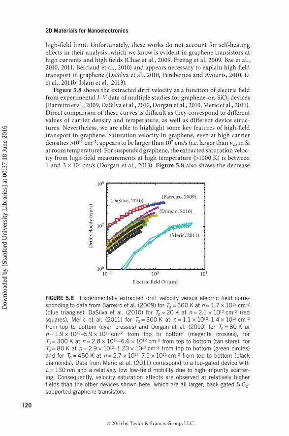
Figure 5.8 shows the extracted drift velocity as a function of electric field from experimental I–V data of multiple studies for graphene-on-SiO2 devices (Barreiro et al., 2009, DaSilva et al., 2010, Dorgan et al., 2010, Meric et al., 2011). Direct comparison of these curves is difficult as they correspond to different values of carrier density and temperature, as well as different device struc-tures. Nevertheless, we are able to highlight some key features of high-field transport in graphene. Saturation velocity in graphene, even at high carrier densities >1013 cm−2, appears to be larger than 107 cm/s (i.e. larger than vsat in Si at room temperature). For suspended graphene, the extracted saturation veloc-ity from high-field measurements at high temperature (>1000 K) is between 1 and 3 × 107 cm/s (Dorgan et al., 2013). Figure 5.8 also shows the decrease
108
(DaSilva, 2010)(Barreiro, 2009)
(Dorgan, 2010)
(Meric, 2011)
Electric field (V/μm)
107
Drif
t vel
ocity
(cm
/s)
10610–1 100 101
FiGUrE 5.8 Experimentally extracted drift velocity versus electric field corre-sponding to data from Barreiro et al. (2009) for T0 = 300 K at n ≈ 1.7 × 1012 cm−2 (blue triangles), DaSilva et al. (2010) for T0 = 20 K at n ≈ 2.1 × 1012 cm−2 (red squares), Meric et al. (2011) for T0 = 300 K at n ≈ 1.1 × 10¹²–1.4 × 1012 cm−2 from top to bottom (cyan crosses) and Dorgan et al. (2010) for T0 = 80 K at n ≈ 1.9 × 10¹²–5.9 × 1012 cm−2 from top to bottom (magenta crosses), for T0 = 300 K at n ≈ 2.8 × 10¹²–6.6 × 1012 cm−2 from top to bottom (tan stars), for T0 = 80 K at n ≈ 2.9 × 10¹²–1.23 × 1013 cm−2 from top to bottom (green circles) and for T0 = 450 K at n ≈ 2.7 × 10¹²–7.5 × 1012 cm−2 from top to bottom (black diamonds). Data from Meric et al. (2011) correspond to a top-gated device with L = 130 nm and a relatively low low-field mobility due to high-impurity scatter-ing. Consequently, velocity saturation effects are observed at relatively higher fields than the other devices shown here, which are all larger, back-gated SiO2-supported graphene transistors.
K24702_Book.indb 120 19-02-2016 14:26:33
© 2016 by Taylor & Francis Group, LLC
Dow
nloa
ded
by [
Stan
ford
Uni
vers
ity L
ibra
ries
] at
00:
37 1
8 Ju
ne 2
016
121
high-Field and thermal transport in Graphene
in high-field drift velocity with increasing carrier density, as mentioned above and shown in previous theoretical works. Similarly, the high-field drift veloc-ity decreases with increasing temperature, which is an expected trend if we assume high-field transport is limited by emission of optical phonons.
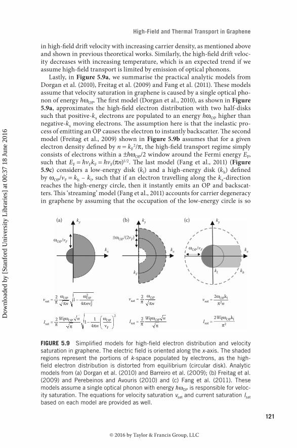
Lastly, in Figure 5.9a, we summarise the practical analytic models from Dorgan et al. (2010), Freitag et al. (2009) and Fang et al. (2011). These models assume that velocity saturation in graphene is caused by a single optical pho-non of energy ħωOP. The first model (Dorgan et al., 2010), as shown in Figure 5.9a, approximates the high-field electron distribution with two half-disks such that positive-kx electrons are populated to an energy ħωOP higher than negative-kx moving electrons. The assumption here is that the inelastic pro-cess of emitting an OP causes the electron to instantly backscatter. The second model (Freitag et al., 2009) shown in Figure 5.9b assumes that for a given electron density defined by n = kF
2/π, the high-field transport regime simply consists of electrons within a ±ħωOP/2 window around the Fermi energy EF, such that EF = ħvFkF = ħvF(πn)1/2. The last model (Fang et al., 2011) (Figure 5.9c) considers a low-energy disk (kl) and a high-energy disk (kh) defined by ωOP/vF = kh – kl, such that if an electron travelling along the kx-direction reaches the high-energy circle, then it instantly emits an OP and backscat-ters. This ‘streaming’ model (Fang et al., 2011) accounts for carrier degeneracy in graphene by assuming that the occupation of the low-energy circle is so
ky(a) (b) (c)ky ky
kx
kF
kx kx
khkl
ωOP/vF
ωOP/vF
±ωOP/(2vF)
vsat = vsat = vsat =
Isat = Isat = Isat = vF
ωOP ωOP 2ωOPkl
2WqωOPklωOPWqωOP WqωOP
ω2OP
πn πn π2n
π2
4πnv2F
π ππ
21n n2
π2
π2
π21–
1–4πn
FiGUrE 5.9 Simplified models for high-field electron distribution and velocity saturation in graphene. The electric field is oriented along the x-axis. The shaded regions represent the portions of k-space populated by electrons, as the high-field electron distribution is distorted from equilibrium (circular disk). Analytic models from (a) Dorgan et al. (2010) and Barreiro et al. (2009); (b) Freitag et al. (2009) and Perebeinos and Avouris (2010) and (c) Fang et al. (2011). These models assume a single optical phonon with energy ħωOP is responsible for veloc-ity saturation. The equations for velocity saturation vsat and current saturation Isat based on each model are provided as well.
K24702_Book.indb 121 19-02-2016 14:26:33
© 2016 by Taylor & Francis Group, LLC
Dow
nloa
ded
by [
Stan
ford
Uni
vers
ity L
ibra
ries
] at
00:
37 1
8 Ju
ne 2
016
122
2D Materials for nanoelectronics
full that the Pauli exclusion principle prohibits an electron with energy less than Eh = ħvFkh to emit an OP, which forces the distribution function to be squeezed and elongated along the direction of the electric field.
We emphasise that these analytic models are more suited for empirical fitting and compact modelling of transistors. It is known that even small changes in the electron distribution can significantly affect charge transport, and thus, these models most likely oversimplify the distribution of carriers during high-field operation. Nevertheless, the compact models give the cor-rect dependence of velocity saturation on carrier density and the magnitude of the phonon responsible (assuming that a single phonon energy is dominant). For example, Dorgan et al. (2010) fit against experimental data using a domi-nant phonon of ~81 meV, which is a value between that of the SiO2 substrate phonon and the intrinsic graphene OP, suggesting that both maybe playing a role – a scenario examined in more depth by Serov et al. (2014).
5.3 thermal transport in Graphene5.3.1 intrinsic thermal Conductivity of GrapheneWe now turn to the discussion of thermal transport in graphene, with impli-cations both for transistors and interconnects. First, we focus on the ‘intrinsic’ thermal conductivity (k) of SLG. Here, by ‘intrinsic’, we mean isolated gra-phene without impurities, defects, interfaces and edge scattering, so its ther-mal conductivity is only limited by intrinsic phonon–phonon scattering due to crystal anharmonicity (Balandin, 2011) and electron–phonon scattering. In experiments, suspended, micrometer scale graphene samples have properties close to intrinsic ones. We thus first summarise current experimental obser-vations of k in suspended SLG.
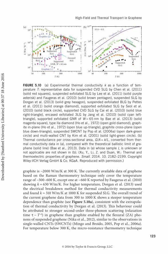
Using the Raman thermometry technique (Balandin, 2011, Xu et al., 2014b), suspended micro-scale graphene flakes obtained by both exfoliation from graphite (Balandin et al., 2008, Ghosh et al., 2008, 2009, 2010, Faugeras et al., 2010; Lee et al., 2011) and CVD growth (Cai et al., 2010, Chen et al., 2011, 2012a,b, Vlassiouk et al., 2011) have been measured at room temperature and above. Some representative data versus temperature from these studies are shown in Figure 5.10a. The obtained in-plane thermal conductivity val-ues of suspended SLG generally fall in the range of ~2000–4000 W/m/K at room temperature, and decrease with increasing temperature, reaching about 700–1500 W/m/K at 500 K. The variation of obtained values could be attrib-uted to different choices of graphene optical absorbance (in the analysis of the Raman data), thermal contact resistance, different sample geometries, sizes and qualities.
For comparison, we also plot the experimental thermal conductivity of diamond (Ho et al., 1972), graphite (Ho et al., 1972) and carbon nanotubes (CNTs) (Kim et al., 2001, Pop et al., 2006a) in Figure 5.10a. It is clear that sus-pended graphene has thermal conductivity as high as these carbon allotropes near room temperature, even higher than its three-dimensional counterpart, graphite, whose in-plane thermal conductivity in highly oriented pyrolytic
K24702_Book.indb 122 19-02-2016 14:26:33
© 2016 by Taylor & Francis Group, LLC
Dow
nloa
ded
by [
Stan
ford
Uni
vers
ity L
ibra
ries
] at
00:
37 1
8 Ju
ne 2
016
123
high-Field and thermal transport in Graphene
graphite is ~2000 W/m/K at 300 K. The currently available data of graphene based on the Raman thermometry technique only cover the temperature range of ~300–600 K, except one at ~660 K reported by Faugeras et al. (2010) showing k ≈ 630 W/m/K. For higher temperature, Dorgan et al. (2013) used the electrical breakdown method for thermal conductivity measurements and found k ≈ 310 W/m/K at 1000 K for suspended SLG. The overall trend of the current graphene data from 300 to 1000 K shows a steeper temperature dependence than graphite (see Figure 5.10a), consistent with the extrapola-tion of thermal conductivity by Dorgan et al. (2013). This behaviour could be attributed to stronger second-order three-phonon scattering (relaxation time τ ~ T −2) in graphene than graphite enabled by the flexural (ZA) pho-nons of suspended graphene (Nika et al., 2012), similar to the observations in single-walled CNTs (SWCNTs) (Mingo and Broido, 2005, Pop et al., 2006a). For temperature below 300 K, the micro-resistance thermometry technique
104
1010
109
108
107
Diamond
103
(a) (b)
102
SuspendedBLG
SuspendedSLG
Suspended BLGSuspended
SLGEncased3LG
SupportedSLG
G/A = k/L
T1.5 T–1
T 2
SupportedGNR, W ≈ 65 nm
50 100 300T (K) T (K)
1000 40 100 300 1000
Supported GNR, W ≈ 65 nm
SupportedSLG
k (W
m–1
K–1)
G/A
(Wm
–2K–1
)
101
Graphite (||) Graphene G ball/A
Graphite (⊥)
MWCNT
MWCNT
SWCNT SWCNT
FiGUrE 5.10 (a) Experimental thermal conductivity k as a function of tem-perature T: representative data for suspended CVD SLG by Chen et al. (2011) (solid red squares), suspended exfoliated SLG by Lee et al. (2011) (solid purple asterisk) and Faugeras et al. (2010) (solid brown pentagon), suspended SLG by Dorgan et al. (2013) (solid grey hexagon), suspended exfoliated BLG by Pettes et al. (2011) (solid orange diamond), supported exfoliated SLG by Seol et al. (2010) (solid black circle), supported CVD SLG by Cai et al. (2010) (solid blue right-triangle), encased exfoliated 3LG by Jang et al. (2010) (solid cyan left-triangle), supported exfoliated GNR of W ≈ 65 nm by Bae et al. (2013) (solid magenta square), type IIa diamond (Ho et al., 1972) (open gold diamond), graph-ite in-plane (Ho et al., 1972) (open blue up-triangle), graphite cross-plane (open blue down-triangle), suspended SWCNT by Pop et al. (2006a) (open dark-green circle) and multi-walled CNT by Kim et al. (2001) (solid light-green circle). (b) Thermal conductance per cross-sectional area, G/A = k/L, converted from ther-mal conductivity data in (a), compared with the theoretical ballistic limit of gra-phene (solid line) (Bae et al., 2013). Data in (a) whose sample L is unknown or not applicable are not shown in (b). (Xu, Y., Li, Z. and Duan, W.: Thermal and thermoelectric properties of graphene. Small. 2014. 10. 2182–2199. Copyright Wiley-VCH Verlag GmbH & Co. KGaA. Reproduced with permission.)
K24702_Book.indb 123 19-02-2016 14:26:34
© 2016 by Taylor & Francis Group, LLC
Dow
nloa
ded
by [
Stan
ford
Uni
vers
ity L
ibra
ries
] at
00:
37 1
8 Ju
ne 2
016
124
2D Materials for nanoelectronics
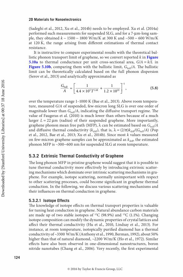
(Sadeghi et al., 2012, Xu et al., 2014b) needs to be employed. Xu et al. (2014a) performed such measurements for suspended SLG, and for a 7-μm-long sam-ple, they obtained k ~ 1500 − 1800 W/m/K at 300 K and ~500 − 600 W/m/K at 120 K, the range arising from different estimations of thermal contact resistance.
It is instructive to compare experimental results with the theoretical bal-listic phonon transport limit of graphene, so we convert reported k in Figure 5.10a to thermal conductance per unit cross-sectional area, G/A = k/L in Figure 5.10b, comparing them with the ballistic limit, Gball/A. The ballistic limit can be theoretically calculated based on the full phonon dispersion (Serov et al., 2013) and analytically approximated as
GA Tball ≈
×+
×
−14 4 10
11 2 105 1 68 10
1
. .,.
(5.8)
over the temperature range 1–1000 K (Bae et al., 2013). Above room tempera-ture, measured G/A of suspended, few-micron long SLG is over one order of magnitude lower than Gball/A, indicating the diffusive transport regime. The value of Faugeras et al. (2010) is much lower than others because of a much larger L = 22 μm (radius) of their suspended graphene. More importantly, graphene phonon mean free path (MFP), λ can be estimated based on Gball/A and diffusive thermal conductivity (kdiff), that is, λ = (2/π)kdiff/(Gball/A) (Pop et al., 2012, Bae et al., 2013; Xu et al., 2014b). Since most k values measured on few-micron graphene samples can be approximated as kdiff, the estimated phonon MFP is ~300−600 nm for suspended SLG at room temperature.
5.3.2 Extrinsic thermal Conductivity of GrapheneThe long phonon MFP in pristine graphene would suggest that it is possible to tune thermal conductivity more effectively by introducing extrinsic scatter-ing mechanisms which dominate over intrinsic scattering mechanisms in gra-phene. For example, isotope scattering, normally unimportant with respect to other scattering processes, could become significant in graphene thermal conduction. In the following, we discuss various scattering mechanisms and their influences on thermal conduction in graphene.
5.3.2.1 isotope EffectsThe knowledge of isotope effects on thermal transport properties is valuable for tuning heat conduction in graphene. Natural abundance carbon materials are made up of two stable isotopes of 12C (98.9%) and 13C (1.1%). Changing isotope composition can modify the dynamic properties of crystal lattices and affect their thermal conductivity (Hu et al., 2010, Lindsay et al., 2013). For instance, at room temperature, isotopically purified diamond has a thermal conductivity of ~3300 W/m/K (Anthony et al., 1990, Berman, 1992), about 50% higher than that of natural diamond, ~2200 W/m/K (Ho et al., 1972). Similar effects have also been observed in one-dimensional nanostructures, boron nitride nanotubes (Chang et al., 2006). Very recently, the first experimental
K24702_Book.indb 124 19-02-2016 14:26:35
© 2016 by Taylor & Francis Group, LLC
Dow
nloa
ded
by [
Stan
ford
Uni
vers
ity L
ibra
ries
] at
00:
37 1
8 Ju
ne 2
016
125
high-Field and thermal transport in Graphene
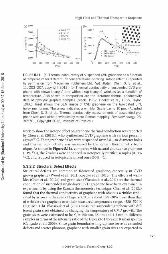
work to show the isotope effect on graphene thermal conduction was reported by Chen et al. (2012b), who synthesized CVD graphene with various percent-ages of 13C. Their graphene flakes were suspended over 2.8-μm-diameter holes and thermal conductivity was measured by the Raman thermometry tech-nique. As shown in Figure 5.11a, compared with natural abundance graphene (1.1% 13C), the k values were enhanced in isotopically purified samples (0.01% 13C), and reduced in isotopically mixed ones (50% 13C).
5.3.2.2 Structural Defect EffectsStructural defects are common in fabricated graphene, especially in CVD grown graphene (Wood et al., 2011, Koepke et al., 2013). The effects of wrin-kles (Chen et al., 2012a) and grain size (Vlassiouk et al., 2011) on the thermal conduction of suspended single-layer CVD graphene have been examined in experiments by using the Raman thermometry technique. Chen et al. (2012a) found that the thermal conductivity of graphene with obvious wrinkles (indi-cated by arrows in the inset of Figure 5.11b) is about 15%–30% lower than that of wrinkle-free graphene over their measured temperature range, ~330–520 K (Figure 5.11b). Vlassiouk et al. (2011) measured suspended graphene with dif-ferent grain sizes obtained by changing the temperature of CVD growth. The grain sizes were estimated to be ℓG = 150 nm, 38 nm and 1.3 nm in different samples in terms of the intensity ratio of the G peak to D peak in Raman spectra (Cançado et al., 2006). Since grain boundaries in graphene serve as extended defects and scatter phonons, graphene with smaller grain sizes are expected to
6000
50004000
3000
2000
1000
00 100 200 300 400 500 600
(a) (b)0.01% 13C1.1% 13C50% 13C99.2% 13C
PG-HookerPG24-Slack With wrinkle
Without wrinkle
PG-Taylor
3000
4000
2000
1000
300 350 400 450T (K) T (K)
500 550 600 650
k (W
m–1
K–1)
k (W
m–1
K–1)
FiGUrE 5.11 (a) Thermal conductivity of suspended CVD graphene as a function of temperature for different 13C concentrations, showing isotope effect. (Reprinted by permission from Macmillan Publishers Ltd. Nat. Mater., Chen, S. S. et al., 11, 203–207, copyright 2012.) (b) Thermal conductivity of suspended CVD gra-phene with (down-triangle) and without (up-triangle) wrinkles as a function of temperature. Also shown in comparison are the literature thermal conductivity data of pyrolytic graphite samples (Slack, 1962, Hooker et al., 1965, Taylor, 1966). Inset shows the SEM image of CVD graphene on the Au-coated SiNx holey membrane. The arrow indicates a wrinkle. Scale bar is 10 μm. (Adapted from Chen, S. S. et al., Thermal conductivity measurements of suspended gra-phene with and without wrinkles by micro-Raman mapping, Nanotechnology, 23, 365701, Copyright 2012, Institute of Physics.)
K24702_Book.indb 125 19-02-2016 14:26:35
© 2016 by Taylor & Francis Group, LLC
Dow
nloa
ded
by [
Stan
ford
Uni
vers
ity L
ibra
ries
] at
00:
37 1
8 Ju
ne 2
016
126
2D Materials for nanoelectronics
suffer more frequent phonon scattering. Their measured thermal conductiv-ity shows the expected decrease for smaller grain sizes, indicating the grain boundary effect on thermal conduction. The dependence on the grain size shows a weak power law, k ~ ℓG
1/3, for which there is no theoretical explana-tion yet (Vlassiouk et al., 2011). However, for SiO2-supported graphene, recent theoretical work based on the NEGF method showed a similar but stronger dependence of k on the grain size ℓG in the range of ℓG < 1 μm (Serov et al., 2013). Further experimental studies are required to reveal the grain size effects on the thermal transport of both suspended and supported graphene.
5.3.2.3 Substrate Effects in Supported GrapheneFor practical applications, graphene is usually in contact with a substrate in electronic and optoelectronic devices, so it is important to understand sub-strate effects on the thermal properties of supported graphene (Ong and Pop, 2011, Guo et al., 2012, Xu and Buehler, 2012, Chen et al., 2013). Seol et al. (2010, 2011) measured exfoliated SLG on a 300-nm-thick SiO2 membrane by using the micro-resistance thermometry technique. The observed thermal conductivity is k ~ 600 W/m/K near room temperature (solid black circles in Figure 5.10a). This value is much lower than those reported for freely suspended SLG via the Raman thermometry technique, but is still relatively high compared with those of bulk silicon (~150 W/m/K) and copper (~400 W/m/K). Another study by Cai et al. (2010) showed CVD SLG supported on Au also has a decreased thermal conductivity, ~370 W/m/K, and this lower value could be caused by grain boundary scattering (Serov et al., 2013). If using 600 W/m/K as kdiff, phonon MFP for SiO2-supported graphene is estimated to be ~90 nm at room temperature (Pop et al., 2012, Bae et al., 2013, Xu et al., 2014b). The thermal conductivity reduction in supported graphene is attributed to substrate scat-tering, which strongly affects the out-of-plane flexural (ZA) mode of graphene (Seol et al., 2010, Ong and Pop, 2011, Qiu and Ruan, 2012). This effect becomes stronger in encased graphene, where graphene is sandwiched between bottom and top SiO2. Jang et al. (2010) measured such SiO2-encased graphene sam-ples using the micro-resistance thermometry technique. The obtained k for encased SLG is reported to be below 160 W/m/K, and that for encased three-layer graphene (3LG) is shown as cyan triangles in Figure 5.10a. For encased graphene, besides the phonon scattering by bottom and top oxides, the depo-sition of the top SiO2 layer could cause defects in graphene, which can further lower thermal conductivity. Knowing the thermal conductivity of supported and encased graphene is useful for analysing heat dissipation in graphene transistors and interconnects.
5.3.2.4 Size Effects and Boundary ScatteringIn macroscopic bulk materials, thermal conductance satisfies Fourier’s scal-ing law in the diffusive region, G = kA/L, where the thermal conductivity k is an intrinsic material property, independent of system size. This scaling law can break down in nanostructures through two mechanisms: (i) non-diffusive (quasi-ballistic) thermal transport and (ii) boundary effects become important. For non-diffusive transport, k becomes length dependent. It is proportional to
K24702_Book.indb 126 19-02-2016 14:26:35
© 2016 by Taylor & Francis Group, LLC
Dow
nloa
ded
by [
Stan
ford
Uni
vers
ity L
ibra
ries
] at
00:
37 1
8 Ju
ne 2
016
127
high-Field and thermal transport in Graphene
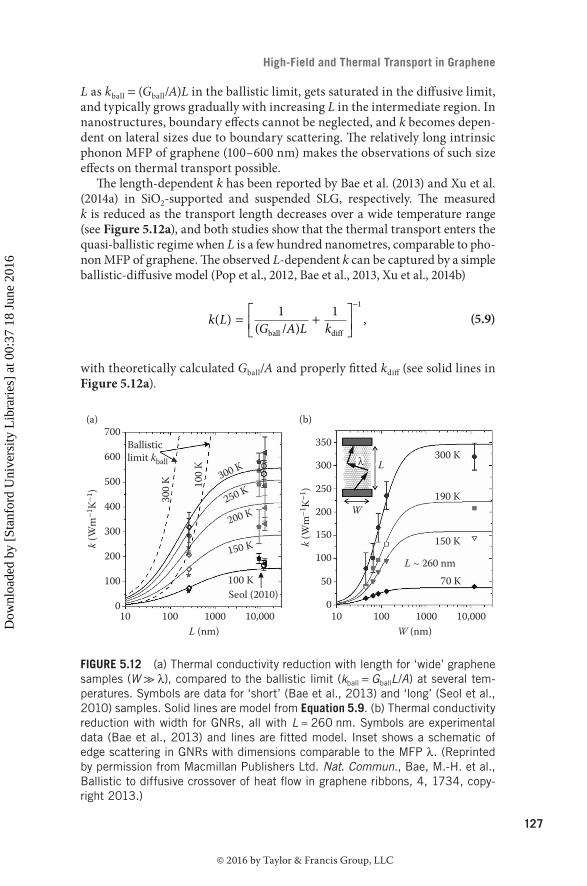
L as kball = (Gball/A)L in the ballistic limit, gets saturated in the diffusive limit, and typically grows gradually with increasing L in the intermediate region. In nanostructures, boundary effects cannot be neglected, and k becomes depen-dent on lateral sizes due to boundary scattering. The relatively long intrinsic phonon MFP of graphene (100–600 nm) makes the observations of such size effects on thermal transport possible.
The length-dependent k has been reported by Bae et al. (2013) and Xu et al. (2014a) in SiO2-supported and suspended SLG, respectively. The measured k is reduced as the transport length decreases over a wide temperature range (see Figure 5.12a), and both studies show that the thermal transport enters the quasi-ballistic regime when L is a few hundred nanometres, comparable to pho-non MFP of graphene. The observed L-dependent k can be captured by a simple ballistic-diffusive model (Pop et al., 2012, Bae et al., 2013, Xu et al., 2014b)
k L
G A L k( )
( ),= +
−1 1
1
ball diff/ (5.9)
with theoretically calculated Gball/A and properly fitted kdiff (see solid lines in Figure 5.12a).
700350
300
250
200
150
100
50
0
(a) (b)
600Ballisticlimit kball
500
400
300
200
100
300 K
250 K
200 K
150 K
0
k (W
m–1
K–1)
k (W
m–1
K–1)
W
Lλ
300
K 100
K
100 K
300 K
190 K
150 K
L ~ 260 nm70 K
Seol (2010)
10 100L (nm)
1000 10,000 10 100W (nm)
1000 10,000
FiGUrE 5.12 (a) Thermal conductivity reduction with length for ‘wide’ graphene samples (W ≫ λ), compared to the ballistic limit (kball = GballL/A) at several tem-peratures. Symbols are data for ‘short’ (Bae et al., 2013) and ‘long’ (Seol et al., 2010) samples. Solid lines are model from Equation 5.9. (b) Thermal conductivity reduction with width for GNRs, all with L ≈ 260 nm. Symbols are experimental data (Bae et al., 2013) and lines are fitted model. Inset shows a schematic of edge scattering in GNRs with dimensions comparable to the MFP λ. (Reprinted by permission from Macmillan Publishers Ltd. Nat. Commun., Bae, M.-H. et al., Ballistic to diffusive crossover of heat flow in graphene ribbons, 4, 1734, copy-right 2013.)
K24702_Book.indb 127 19-02-2016 14:26:36
© 2016 by Taylor & Francis Group, LLC
Dow
nloa
ded
by [
Stan
ford
Uni
vers
ity L
ibra
ries
] at
00:
37 1
8 Ju
ne 2
016
128
2D Materials for nanoelectronics
The lateral size effects, that is, width-dependence of graphene ther-mal transport has also been measured by Bae et al. (2013) on GNRs with W ~ 45–130 nm, implemented by developing a substrate-supported ther-mometry platform (Li et al., 2014). The significant decrease of k is observed when W < 200 nm (see Figure 5.12b), due to increased edge scattering in nar-rower GNRs (see inset of Figure 5.12b). Through electrical breakdown mea-surements, Liao et al. (2011) were able to estimate k of CNT-unzipped GNRs (Jiao et al., 2009). Although the obtained values are slightly higher than those of Bae et al. (2013) for similar widths, considering that CNT-unzipped GNRs have smoother edges (Jiao et al., 2009, Kosynkin et al., 2009) (less edge rough-ness scattering), the two studies are essentially consistent.
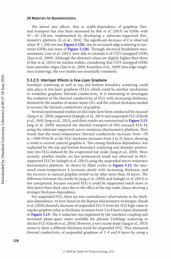
5.3.2.5 interlayer Effects in Few-Layer GrapheneInterlayer scattering as well as top and bottom boundary scattering could take place in few-layer graphene (FLG), which could be another mechanism to modulate graphene thermal conductivity. It is interesting to investigate the evolution of the thermal conductivity of FLG with increasing thickness, denoted by the number of atomic layers (N), and the critical thickness needed to recover the thermal conductivity of graphite.
Several experimental studies on this topic have been conducted for encased (Jang et al., 2010), supported (Sadeghi et al., 2013) and suspended FLG (Ghosh et al., 2010, Jang et al., 2013), and their results are summarised in Figure 5.13. Jang et al. (2010) measured the thermal transport of SiO2-encased FLG by using the substrate-supported, micro-resistance thermometry platform. They found that the room-temperature thermal conductivity increases from ~50 to ~1000 W/m/K as the FLG thickness increases from 2 to 21 layers, showing a trend to recover natural graphite k. This strong thickness dependence was explained by the top and bottom boundary scattering and disorder penetra-tion into FLG induced by the evaporated top oxide (Jang et al., 2010). More recently, another similar yet less pronounced trend was observed in SiO2-supported FLG by Sadeghi et al. (2013) using the suspended micro-resistance thermometry platform. As shown by filled circles in Figure 5.13, the mea-sured room-temperature k increases slowly with increasing thickness, and the recovery to natural graphite would occur after more than 34 layers. The difference between the results by Jang et al. (2010) and Sadeghi et al. (2013) is not unexpected, because encased FLG k could be suppressed much more in thin layers than thick ones due to the effect of the top oxide, hence showing a stronger thickness dependence.
For suspended FLG, there are two contradictory observations in the thick-ness dependence. At first, based on the Raman thermometry technique, Ghosh et al. (2010) showed a decrease of suspended FLG k from the SLG high value to regular graphite value as thickness increases from 2 to 8 layers (open diamonds in Figure 5.13). The k reduction was explained by the interlayer coupling and increased phase-space states available for phonon Umklapp scattering in thicker FLG (Ghosh et al., 2010). However, a very recent study (Jang et al., 2013) seems to show a different thickness trend for suspended FLG. They measured thermal conductivity of suspended graphene of 2–4 and 8 layers by using a
K24702_Book.indb 128 19-02-2016 14:26:36
© 2016 by Taylor & Francis Group, LLC
Dow
nloa
ded
by [
Stan
ford
Uni
vers
ity L
ibra
ries
] at
00:
37 1
8 Ju
ne 2
016
129
high-Field and thermal transport in Graphene
modified T-bridge micro-resistance thermometry technique. The obtained room-temperature k for 2–4 layers is about 300–400 W/m/K with no apparent thickness dependence, whereas k for 8-layer shows an increase to ~600 W/m/K (open squares in Figure 5.13). Surprisingly, this trend is qualitatively in agree-ment with that of Sadeghi et al. (2013) for supported FLG; both show simi-lar increasing amounts of k from 2 to 8 layers (Figure 5.13), despite a small decrease from 2 to 4 layers in the former, which could arise from different sample qualities and measurement uncertainty. Given the opposite thickness trends of Ghosh et al. (2010) and Jang et al. (2013), further experiments are required to clarify the real thickness-dependent k in suspended FLG.
5.3.2.6 Cross-Plane thermal ConductionA remarkable feature of graphite and graphene is that their thermal proper-ties are highly anisotropic. Despite high thermal conductivity along the in-plane direction, heat flow along the cross-plane direction (c-axis) is hundreds of times weaker, limited by weak van der Waals interactions between lay-ers (for graphite) or with adjacent materials (for graphene). For example, the
1000
SuspendedJang et al.
1 10Number of layers
SuspendedGhosh et al.
Natural graphite
SupportedSadeghi et al.
EncasedJang et al.
T ~ 300 K
100
k (W
m–1
K–1)
FiGUrE 5.13 Experimental in-plane thermal conductivity near room temperature as a function of the number of layers N for suspended graphene by Ghosh et al. (2010) (open diamond) and Jang et al. (2013) (open square), SiO2-supported gra-phene by Seol et al. (2010) (open circle) and Sadeghi et al. (2013) (solid circle) and SiO2-encased graphene by Jang et al. (2010) (solid black triangle). The data show a trend to recover the value (dashed line) measured by Sadeghi et al. (2013) for natural graphite source used to exfoliate graphene. The grey-shaded area shows the highest reported k values of pyrolytic graphite (Slack, 1962, Hooker et al., 1965, Taylor, 1966). (Sadeghi, M. M., Jo, I. and Shi, L. Phonon-interface scattering in multilayer graphene on an amorphous support. Proc. Natl. Acad. Sci. USA, 110, 16321–16326, Copyright 2013 National Academy of Sciences, U.S.A.)
K24702_Book.indb 129 19-02-2016 14:26:36
© 2016 by Taylor & Francis Group, LLC
Dow
nloa
ded
by [
Stan
ford
Uni
vers
ity L
ibra
ries
] at
00:
37 1
8 Ju
ne 2
016
130
2D Materials for nanoelectronics
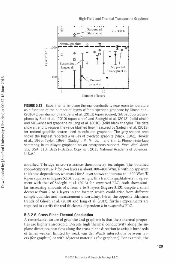
thermal conductivity along the c-axis of pyrolytic graphite is only ~6 W/m/K at room temperature (Ho et al., 1972) (Figure 5.10a). For graphene, as it is often attached to a substrate or embedded in a medium, heat conduction in the cross-plane direction is characterised by the thermal interface resistance (or conductance, G⊥) with adjacent materials, which could become a limiting dissipation bottleneck in highly scaled graphene devices and interconnects (Bae et al., 2010, 2011, Behnam et al., 2012, Pop et al., 2012, Islam et al., 2013).
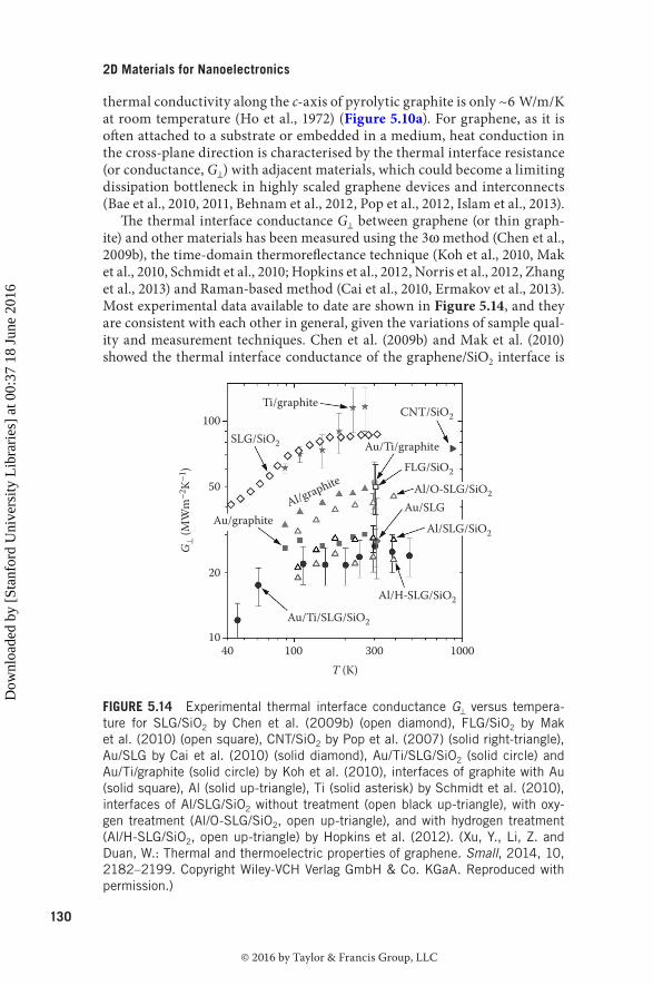
The thermal interface conductance G⊥ between graphene (or thin graph-ite) and other materials has been measured using the 3ω method (Chen et al., 2009b), the time-domain thermoreflectance technique (Koh et al., 2010, Mak et al., 2010, Schmidt et al., 2010; Hopkins et al., 2012, Norris et al., 2012, Zhang et al., 2013) and Raman-based method (Cai et al., 2010, Ermakov et al., 2013). Most experimental data available to date are shown in Figure 5.14, and they are consistent with each other in general, given the variations of sample qual-ity and measurement techniques. Chen et al. (2009b) and Mak et al. (2010) showed the thermal interface conductance of the graphene/SiO2 interface is
100
50
Ti/graphiteCNT/SiO2
Au/Ti/graphiteFLG/SiO2
SLG/SiO2
Au/graphite
G⊥
(MW
m–2
K–1)
Al/graphite Al/O-SLG/SiO2Au/SLG
Al/SLG/SiO2
Al/H-SLG/SiO2
Au/Ti/SLG/SiO2
20
1040 100 300
T (K)1000
FiGUrE 5.14 Experimental thermal interface conductance G⊥ versus tempera-ture for SLG/SiO2 by Chen et al. (2009b) (open diamond), FLG/SiO2 by Mak et al. (2010) (open square), CNT/SiO2 by Pop et al. (2007) (solid right-triangle), Au/SLG by Cai et al. (2010) (solid diamond), Au/Ti/SLG/SiO2 (solid circle) and Au/Ti/graphite (solid circle) by Koh et al. (2010), interfaces of graphite with Au (solid square), Al (solid up-triangle), Ti (solid asterisk) by Schmidt et al. (2010), interfaces of Al/SLG/SiO2 without treatment (open black up-triangle), with oxy-gen treatment (Al/O-SLG/SiO2, open up-triangle), and with hydrogen treatment (Al/H-SLG/SiO2, open up-triangle) by Hopkins et al. (2012). (Xu, Y., Li, Z. and Duan, W.: Thermal and thermoelectric properties of graphene. Small, 2014, 10, 2182–2199. Copyright Wiley-VCH Verlag GmbH & Co. KGaA. Reproduced with permission.)
K24702_Book.indb 130 19-02-2016 14:26:37
© 2016 by Taylor & Francis Group, LLC
Dow
nloa
ded
by [
Stan
ford
Uni
vers
ity L
ibra
ries
] at
00:
37 1
8 Ju
ne 2
016
131
high-Field and thermal transport in Graphene
G⊥ ~ 50–100 MW/m2/K at room temperature, with no strong dependence on the FLG thickness. Their values are close to that of CNT/SiO2 (Pop et al., 2007), reflecting the similarity between graphene and CNT. Schmidt et al. (2010) measured G⊥ of graphite–metal interfaces, including Au, Cr, Al and Ti. Among them, the graphite–Ti interface has the highest G⊥ ~ 120 MW/m2/K and the graphite–Au interface has the lowest G⊥ ~ 30 MW/m2/K near room temperature. The G⊥ of graphite–Au is consistent with the value by Norris et al. (2012) and values of SLG–Au by Cai et al. (2010) and FLG/Au by Ermakov et al. (2013). Koh et al. (2010) later measured heat flow across the Au/Ti/N-LG/SiO2 interfaces with the layer number N = 1 − 10. Their observed room-tem-perature G⊥ was ~25 MW/m2/K, which shows a very weak dependence on the layer number N and is equivalent to the total thermal conductance of Au–Ti–graphite and graphene–SiO2 interfaces acting in series. This indicates that the thermal resistance of two interfaces between graphene and its environ-ment dominates over that between graphene layers. Interestingly, Hopkins et al. (2012) showed the thermal conduction across the Al–SLG–SiO2 interface could be manipulated by introducing chemical adsorbates between the Al and SLG. As shown in Figure 5.14, their measured G⊥ of untreated Al/SLG/SiO2 is ~30 MW/m2/K at room temperature, in agreement with Zhang et al. (2013). The G⊥ increases to ~42 MW/m2/K for oxygen-functionalised gra-phene (O-SLG), and decreases to ~23 MW/m2/K for hydrogen-functionalised graphene (H-SLG). These effects were attributed to changes in chemical bond-ing between the metal and graphene, and are consistent with the observed enhancement in G⊥ from the Al/diamond (Stoner et al., 1992) to Al/O-diamond interfaces (Collins et al., 2010).
referencesAdam, S., Hwang, E. H., Galitski, V. M. and Das Sarma, S. 2007. A self-consistent
theory for graphene transport. Proc. Natl. Acad. Sci. USA, 104, 18392–18397.Adam, S., Hwang, E. H., Rossi, E. and Sarma, S. D. 2009. Theory of charged impurity
scattering in two-dimensional graphene. Solid State Commun., 149, 1072–1079.Akturk, A. and Goldsman, N. 2008. Electron transport and full-band electron–pho-
non interactions in graphene. J. Appl. Phys., 103, 053702.Ancona, M. G. 2010. Electron transport in graphene from a diffusion-drift perspec-
tive. IEEE Trans. Electron Devices, 57, 681–689.Anthony, T. R., Banholzer, W. F., Fleischer, J. F., Wei, L. H., Kuo, P. K., Thomas, R. L.
and Pryor, R. W. 1990. Thermal-diffusivity of isotopically enriched C-12 dia-mond. Phys. Rev. B, 42, 1104–1111.
Bae, M.-H., Islam, S., Dorgan, V. E. and Pop, E. 2011. Scaling of high-field transport and localized heating in graphene transistors. ACS Nano, 5, 7936–7944.
Bae, M.-H., Li, Z., Aksamija, Z., Martin, P. N., Xiong, F., Ong, Z.-Y., Knezevic, I. and Pop, E. 2013. Ballistic to diffusive crossover of heat flow in graphene ribbons. Nat. Commun., 4, 1734.
Bae, M. H., Ong, Z. Y., Estrada, D. and Pop, E. 2010. Imaging, simulation and electro-static control of power dissipation in graphene devices. Nano Lett., 10, 4787–4793.
Balandin, A. A. 2011. Thermal properties of graphene and nanostructured carbon materials. Nat. Mater., 10, 569–581.
K24702_Book.indb 131 19-02-2016 14:26:37
© 2016 by Taylor & Francis Group, LLC
Dow
nloa
ded
by [
Stan
ford
Uni
vers
ity L
ibra
ries
] at
00:
37 1
8 Ju
ne 2
016
132
2D Materials for nanoelectronics
Balandin, A. A., Ghosh, S., Bao, W. Z., Calizo, I., Teweldebrhan, D., Miao, F. and Lau, C. N. 2008. Superior thermal conductivity of single-layer graphene. Nano Lett., 8, 902–907.
Barreiro, A., Lazzeri, M., Moser, J., Mauri, F. and Bachtold, A. 2009. Transport proper-ties of graphene in the high-current limit. Phys. Rev. Lett., 103, 076601.
Behnam, A., Lyons, A. S., Bae, M.-H., Chow, E. K., Islam, S., Neumann, C. M. and Pop, E. 2012. Transport in nanoribbon interconnects obtained from graphene grown by chemical vapor deposition. Nano Lett., 12, 4424–4430.
Berciaud, S., Han, M. Y., Mak, K. F., Brus, L. E., Kim, P. and Heinz, T. F. 2010. Electron and optical phonon temperatures in electrically biased graphene. Phys. Rev. Lett., 104, 227401.
Berman, R. 1992. Thermal-conductivity of isotopically enriched diamonds. Phys. Rev. B, 45, 5726–5728.
Biro, L. P., Nemes-Incze, P. and Lambin, P. 2012. Graphene: Nanoscale processing and recent applications. Nanoscale, 4, 1824–1839.
Bistritzer, R. and Macdonald, A. H. 2009. Hydrodynamic theory of transport in doped graphene. Phys. Rev. B, 80, 085109.
Bolotin, K. I., Sikes, K. J., Jiang, Z., Klima, M., Fudenberg, G., Hone, J., Kim, P. and Stormer, H. L. 2008. Ultrahigh electron mobility in suspended graphene. Solid State Commun., 146, 351–355.
Borysenko, K. M., Mullen, J. T., Barry, E. A., Paul, S., Semenov, Y. G., Zavada, J. M., Nardelli, M. B. and Kim, K. W. 2010. First-principles analysis of electron–pho-non interactions in graphene. Phys. Rev. B, 81, 121412.
Cai, W. W., Moore, A. L., Zhu, Y. W., Li, X. S., Chen, S. S., Shi, L. and Ruoff, R. S. 2010. Thermal transport in suspended and supported monolayer graphene grown by chemical vapor deposition. Nano Lett., 10, 1645–1651.
Cançado, L. G., Takai, K., Enoki, T., Endo, M., Kim, Y. A., Mizusaki, H., Jorio, A., Coelho, L. N., Magalhães-Paniago, R. and Pimenta, M. A. 2006. General equa-tion for the determination of the crystallite size La of nanographite by Raman spectroscopy. Appl. Phys. Lett., 88, 163106.
Castro Neto, A. H., Guinea, F., Peres, N. M. R., Novoselov, K. S. and Geim, A. K. 2009. The electronic properties of graphene. Rev. Mod. Phys., 81, 109–162.
Chae, D.-H., Krauss, B., von Klitzing, K. and Smet, J. H. 2009. Hot phonons in an elec-trically biased graphene constriction. Nano Lett., 10, 466–471.
Chang, C. W., Fennimore, A. M., Afanasiev, A., Okawa, D., Ikuno, T., Garcia, H., Li, D. Y., Majumdar, A. and Zettl, A. 2006. Isotope effect on the thermal conductivity of boron nitride nanotubes. Phys. Rev. Lett., 97, 085901.
Chauhan, J. and Guo, J. 2009. High-field transport and velocity saturation in gra-phene. Appl. Phys. Lett., 95, 023120.
Chen, F., Xia, J. and Tao, N. 2009a. Ionic screening of charged-impurity scattering in graphene. Nano Lett., 9, 1621–1625.
Chen, I. J., Mante, P. A., Chang, C. K., Yang, S. C., Chen, H. Y., Huang, Y. R., Chen, L. C., Chen, K. H., Gusev, V. and Sun, C. K. 2014. Graphene-to-substrate energy transfer through out-of-plane longitudinal acoustic phonons. Nano Lett., 14, 1317–1323.
Chen, J., Zhang, G. and Li, B. W. 2013. Substrate coupling suppresses size dependence of thermal conductivity in supported graphene. Nanoscale, 5, 532–536.
Chen, J. H., Jang, C., Adam, S., Fuhrer, M. S., Williams, E. D. and Ishigami, M. 2008. Charged-impurity scattering in graphene. Nat. Phys., 4, 377–381.
Chen, S. S., Li, Q. Y., Zhang, Q. M., Qu, Y., Ji, H. X., Ruoff, R. S. and Cai, W. W. 2012a. Thermal conductivity measurements of suspended graphene with and without wrinkles by micro-Raman mapping. Nanotechnology, 23, 365701.
K24702_Book.indb 132 19-02-2016 14:26:37
© 2016 by Taylor & Francis Group, LLC
Dow
nloa
ded
by [
Stan
ford
Uni
vers
ity L
ibra
ries
] at
00:
37 1
8 Ju
ne 2
016
133
high-Field and thermal transport in Graphene
Chen, S. S., Moore, A. L., Cai, W. W., Suk, J. W., An, J. H., Mishra, C., Amos, C. et al. 2011. Raman measurements of thermal transport in suspended monolayer graphene of variable sizes in vacuum and gaseous environments. ACS Nano, 5, 321–328.
Chen, S. S., Wu, Q. Z., Mishra, C., Kang, J. Y., Zhang, H. J., Cho, K. J., Cai, W. W., Balandin, A. A. and Ruoff, R. S. 2012b. Thermal conductivity of isotopically modified graphene. Nat. Mater., 11, 203–207.
Chen, Z., Jang, W., Bao, W., Lau, C. N. and Dames, C. 2009b. Thermal contact resis-tance between graphene and silicon dioxide. Appl. Phys. Lett., 95, 161910.
Collins, K. C., Chen, S. and Chen, G. 2010. Effects of surface chemistry on thermal conductance at aluminum–diamond interfaces. Appl. Phys. Lett., 97, 083102.
Dasilva, A. M., Zou, K., Jain, J. K. and Zhu, J. 2010. Mechanism for current saturation and energy dissipation in graphene transistors. Phys. Rev. Lett., 104, 236601.
Deshpande, A., Bao, W., Miao, F., Lau, C. N. and Leroy, B. J. 2009. Spatially resolved spectroscopy of monolayer graphene on SiO2. Phys. Rev. B, 79, 205411.
Dorgan, V. E., Bae, M.-H. and Pop, E. 2010. Mobility and saturation velocity in gra-phene on SiO2. Appl. Phys. Lett., 97, 082112.
Dorgan, V. E., Behnam, A., Conley, H. J., Bolotin, K. I. and Pop, E. 2013. High-field elec-trical and thermal transport in suspended graphene. Nano Lett., 13, 4581–4586.
Ermakov, V. A., Alaferdov, A. V., Vaz, A. R., Baranov, A. V. and Moshkalev, S. A. 2013. Nonlocal laser annealing to improve thermal contacts between multi-layer gra-phene and metals. Nanotechnology, 24, 155301.
Fang, T., Konar, A., Xing, H. and Jena, D. 2007. Carrier statistics and quantum capaci-tance of graphene sheets and ribbons. Appl. Phys. Lett., 91, 092109.
Fang, T., Konar, A., Xing, H. and Jena, D. 2011. High-field transport in two-dimen-sional graphene. Phys. Rev. B, 84, 125450.
Faugeras, C., Faugeras, B., Orlita, M., Potemski, M., Nair, R. R. and Geim, A. K. 2010. Thermal conductivity of graphene in corbino membrane geometry. ACS Nano, 4, 1889–1892.
Ferry, D. K. 2012. The role of substrate for transport in graphene. IEEE Nanotechnology Materials and Devices Conference, 16–19 October 2012, Waikiki Beach, HI, 43–48.
Fischetti, M. V., Kim, J., Narayanan, S., Ong, Z.-Y., Sachs, C., Ferry, D. K. and Aboud, S. J. 2013. Pseudopotential-based studies of electron transport in graphene and graphene nanoribbons. J. Phys. Condens. Matter, 25, 473202.
Fischetti, M. V., Neumayer, D. A. and Cartier, E. A. 2001. Effective electron mobility in Si inversion layers in metal–oxide–semiconductor systems with a high-κ insula-tor: The role of remote phonon scattering. J. Appl. Phys., 90, 4587–4608.
Freitag, M., Steiner, M., Martin, Y., Perebeinos, V., Chen, Z., Tsang, J. C. and Avouris, P. 2009. Energy dissipation in graphene field-effect transistors. Nano Lett., 9, 1883–1888.
Geim, A. K. 2011. Nobel lecture: Random walk to graphene. Rev. Mod. Phys., 83, 851–862.
Geim, A. K. and Novoselov, K. S. 2007. The rise of graphene. Nat. Mater., 6, 183–191.Ghosh, S., Bao, W., Nika, D. L., Subrina, S., Pokatilov, E. P., Lau, C. N. and Balandin,
A. A. 2010. Dimensional crossover of thermal transport in few-layer graphene. Nat. Mater., 9, 555–558.
Ghosh, S., Calizo, I., Teweldebrhan, D., Pokatilov, E. P., Nika, D. L., Balandin, A. A., Bao, W., Miao, F. and Lau, C. N. 2008. Extremely high thermal conductivity of graphene: Prospects for thermal management applications in nanoelectronic circuits. Appl. Phys. Lett., 92, 151911.
Ghosh, S., Nika, D. L., Pokatilov, E. P. and Balandin, A. A. 2009. Heat conduction in gra-phene: Experimental study and theoretical interpretation. New J. Phys., 11, 095012.
K24702_Book.indb 133 19-02-2016 14:26:37
© 2016 by Taylor & Francis Group, LLC
Dow
nloa
ded
by [
Stan
ford
Uni
vers
ity L
ibra
ries
] at
00:
37 1
8 Ju
ne 2
016
134
2D Materials for nanoelectronics
Girdhar, A. and Leburton, J. P. 2011. Soft carrier multiplication by hot electrons in graphene. Appl. Phys. Lett., 99, 043107.
Guo, Z. X., Ding, J. W. and Gong, X. G. 2012. Substrate effects on the thermal conduc-tivity of epitaxial graphene nanoribbons. Phys. Rev. B, 85, 235429.
Han, M. Y., Ozyilmaz, B., Zhang, Y. B. and Kim, P. 2007. Energy band-gap engineering of graphene nanoribbons. Phys. Rev. Lett., 98, 206805.
Hess, K. and Vogl, P. 1979. Remote polar phonon scattering in silicon inversion layers. Solid State Commun., 30, 797–799.
Ho, C. Y., Powell, R. W. and Liley, P. E. 1972. Thermal conductivity of the elements. J. Phys. Chem. Ref. Data, 1, 279–421.
Hooker, C. N., Ubbelohd, A. R. and Young, D. A. 1965. Anisotropy of thermal conduc-tance in near-ideal graphite. Proc. R. Soc. Lon. A, 284, 17–31.
Hopkins, P. E., Baraket, M., Barnat, E. V., Beechem, T. E., Kearney, S. P., Duda, J. C., Robinson, J. T. and Walton, S. G. 2012. Manipulating thermal conductance at metal–graphene contacts via chemical functionalization. Nano Lett., 12, 590–595.
Hu, J. N., Schiffli, S., Vallabhaneni, A., Ruan, X. L. and Chen, Y. P. 2010. Tuning the thermal conductivity of graphene nanoribbons by edge passivation and isotope engineering: A molecular dynamics study. Appl. Phys. Lett., 97, 133107.
Huang, B., Yan, Q., Li, Z. and Duan, W. 2009. Towards graphene nanoribbon-based electronics. Front. Phys. China, 4, 269–279.
Huang, P. Y., Ruiz-Vargas, C. S., van der Zande, A. M., Whitney, W. S., Levendorf, M. P., Kevek, J. W., Garg, S. et al. 2011. Grains and grain boundaries in single-layer graphene atomic patchwork quilts. Nature, 469, 389–392.
Ishigami, M., Chen, J. H., Cullen, W. G., Fuhrer, M. S. and Williams, E. D. 2007. Atomic structure of graphene on SiO2. Nano Lett., 7, 1643–1648.
Islam, S., Li, Z., Dorgan, V. E., Bae, M.-H. and Pop, E. 2013. Role of joule heating on current saturation and transient behavior of graphene transistors. IEEE Electron Device Lett., 34, 166–168.
Jacoboni, C., Canali, C., Ottaviani, G. and Alberigi Quaranta, A. 1977. A review of some charge transport properties of silicon. Solid-State Electron., 20, 77–89.
Jacoboni, C. and Reggiani, L. 1983. The Monte Carlo method for the solution of charge transport in semiconductors with applications to covalent materials. Rev. Mod. Phys., 55, 645–705.
Jang, W., Bao, W., Jing, L., Lau, C. N. and Dames, C. 2013. Thermal conductivity of suspended few-layer graphene by a modified T-bridge method. Appl. Phys. Lett., 103, 133102.
Jang, W. Y., Chen, Z., Bao, W. Z., Lau, C. N. and Dames, C. 2010. Thickness-dependent thermal conductivity of encased graphene and ultrathin graphite. Nano Lett., 10, 3909–3913.
Jiao, L., Zhang, L., Wang, X., Diankov, G. and Dai, H. 2009. Narrow graphene nanorib-bons from carbon nanotubes. Nature, 458, 877–880.
Jimenez, D. 2011. Explicit drain current, charge and capacitance model of graphene field-effect transistors. IEEE Trans. Electron Devices, 58, 4377–4383.
Kedzierski, J., Hsu, P.-L., Healey, P., Wyatt, P. W., Keast, C. L., Sprinkle, M., Berger, C. and de Heer, W. A. 2008. Epitaxial graphene transistors on SiC substrates. IEEE Trans. Electron Devices, 55, 2078–2085.
Kim, E., Jain, N., Jacobs-Gedrim, R., Xu, Y. and Yu, B. 2012. Exploring carrier trans-port phenomena in a CVD-assembled graphene FET on hexagonal boron nitride. Nanotechnology, 23, 125706.
K24702_Book.indb 134 19-02-2016 14:26:37
© 2016 by Taylor & Francis Group, LLC
Dow
nloa
ded
by [
Stan
ford
Uni
vers
ity L
ibra
ries
] at
00:
37 1
8 Ju
ne 2
016
135
high-Field and thermal transport in Graphene
Kim, K. S., Zhao, Y., Jang, H., Lee, S. Y., Kim, J. M., Kim, K. S., Ahn, J. H., Kim, P., Choi, J. Y. and Hong, B. H. 2009a. Large-scale pattern growth of graphene films for stretchable transparent electrodes. Nature, 457, 706–710.
Kim, P., Shi, L., Majumdar, A. and Mceuen, P. L. 2001. Thermal transport measure-ments of individual multiwalled nanotubes. Phys. Rev. Lett., 87, 215502.
Kim, S., Nah, J., Jo, I., Shahrjerdi, D., Colombo, L., Yao, Z., Tutuc, E. and Banerjee, S. K. 2009b. Realization of a high mobility dual-gated graphene field-effect transis-tor with Al2O3 dielectric. Appl. Phys. Lett., 94, 062107.
Koepke, J. C., Wood, J. D., Estrada, D., Ong, Z. Y., He, K. T., Pop, E. and Lyding, J. W. 2013. Atomic-scale evidence for potential barriers and strong carrier scatter-ing at graphene grain boundaries: A scanning tunneling microscopy study. ACS Nano, 7, 75–86.
Koh, Y. K., Bae, M.-H., Cahill, D. G. and Pop, E. 2010. Heat conduction across mono-layer and few-layer graphenes. Nano Lett., 10, 4363–4368.
Kosynkin, D. V., Higginbotham, A. L., Sinitskii, A., Lomeda, J. R., Dimiev, A., Price, B. K. and Tour, J. M. 2009. Longitudinal unzipping of carbon nanotubes to form graphene nanoribbons. Nature, 458, 872–875.
Leburton, J. P. and Dorda, G. 1981. Remote polar phonon scattering for hot electrons in Si-inversion layers. Solid State Commun., 40, 1025–1026.
Lee, C., Wei, X., Kysar, J. W. and Hone, J. 2008. Measurement of the elastic properties and intrinsic strength of monolayer graphene. Science, 321, 385–388.
Lee, J. U., Yoon, D., Kim, H., Lee, S. W. and Cheong, H. 2011. Thermal conductivity of suspended pristine graphene measured by Raman spectroscopy. Phys. Rev. B, 83, 081419.
Li, Q., Hwang, E. H. and Das Sarma, S. 2011a. Disorder-induced temperature-depen-dent transport in graphene: Puddles, impurities, activation and diffusion. Phys. Rev. B, 84, 115442.
Li, X., Barry, E. A., Zavada, J. M., Nardelli, M. B. and Kim, K. W. 2010. Surface polar phonon dominated electron transport in graphene. Appl. Phys. Lett., 97, 232105.
Li, X., Cai, W., An, J., Kim, S., Nah, J., Yang, D., Piner, R., Velamakanni, A., Jung, I. and Tutuc, E. 2009. Large-area synthesis of high-quality and uniform graphene films on copper foils. Science, 324, 1312–1314.
Li, X., Kong, B., Zavada, J. and Kim, K. 2011b. Strong substrate effects of Joule heating in graphene electronics. Appl. Phys. Lett., 99, 233114.
Li, X. L., Wang, X. R., Zhang, L., Lee, S. W. and Dai, H. J. 2008. Chemically derived, ultrasmooth graphene nanoribbon semiconductors. Science, 319, 1229–1232.
Li, Z., Bae, M.-H. and Pop, E. 2014. Substrate-supported thermometry platform for nanomaterials like graphene, nanotubes and nanowires. Appl. Phys. Lett., 105, 023107.
Liao, A. D., Wu, J. Z., Wang, X., Tahy, K., Jena, D., Dai, H. and Pop, E. 2011. Thermally limited current carrying ability of graphene nanoribbons. Phys. Rev. Lett., 106, 256801.
Lin, Y.-M., Dimitrakopoulos, C., Jenkins, K. A., Farmer, D. B., Chiu, H.-Y., Grill, A. and Avouris, P. 2010. 100-GHz transistors from wafer-scale epitaxial graphene. Science, 327, 662–662.
Lindsay, L., Broido, D. A. and Mingo, N. 2010. Flexural phonons and thermal trans-port in graphene. Phys. Rev. B, 82, 115427.
Lindsay, L., Broido, D. A. and Reinecke, T. L. 2013. Phonon-isotope scattering and thermal conductivity in materials with a large isotope effect: A first-principles study. Phys. Rev. B, 88, 144306.
K24702_Book.indb 135 19-02-2016 14:26:37
© 2016 by Taylor & Francis Group, LLC
Dow
nloa
ded
by [
Stan
ford
Uni
vers
ity L
ibra
ries
] at
00:
37 1
8 Ju
ne 2
016
136
2D Materials for nanoelectronics
Lundstrom, M. 2000. Fundamentals of Carrier Transport. Cambridge University Press, Cambridge, UK.
Mak, K. F., Lui, C. H. and Heinz, T. F. 2010. Measurement of the thermal conductance of the graphene/SiO2 interface. Appl. Phys. Lett., 97, 221904.
Martin, J., Akerman, N., Ulbricht, G., Lohmann, T., Smet, J. H., Von Klitzing, K. and Yacoby, A. 2008. Observation of electron–hole puddles in graphene using a scanning single-electron transistor. Nat. Phys., 4, 144–148.
Meric, I., Dean, C. R., Young, A. F., Baklitskaya, N., Tremblay, N. J., Nuckolls, C., Kim, P. and Shepard, K. L. 2011. Channel length scaling in graphene field-effect transistors studied with pulsed current − voltage measurements. Nano Lett., 11, 1093–1097.
Meric, I., Han, M. Y., Young, A. F., Ozyilmaz, B., Kim, P. and Shepard, K. L. 2008. Current saturation in zero-bandgap, top-gated graphene field-effect transistors. Nat. Nanotechnol., 3, 654–659.
Mingo, N. and Broido, D. A. 2005. Length dependence of carbon nanotube thermal conductivity and the ‘problem of long waves’. Nano Lett., 5, 1221–1225.
Mohr, M., Maultzsch, J., Dobardzic, E., Reich, S., Milosevic, I., Damnjanovic, M., Bosak, A., Krisch, M. and Thomsen, C. 2007. Phonon dispersion of graphite by inelastic x-ray scattering. Phys. Rev. B, 76, 035439.
Moore, B. T. and Ferry, D. K. 1980. Remote polar phonon scattering in Si inversion layers. J. Appl. Phys., 51, 2603–2605.
Muller, R. S., Kamins, T. I. and Chan, M. 2003. Device Electronics for Integrated Circuits. John Wiley and Sons, New York.
Nika, D. L., Askerov, A. S. and Balandin, A. A. 2012. Anomalous size dependence of the thermal conductivity of graphene ribbons. Nano Lett., 12, 3238–3244.
Norris, P. M., Smoyer, J. L., Duda, J. C. and Hopkins, P. E. 2012. Prediction and mea-surement of thermal transport across interfaces between isotropic solids and graphitic materials. J. Heat Transf., 134, 020910.
Novoselov, K. S. 2011. Nobel lecture: Graphene: Materials in the flatland. Rev. Mod. Phys., 83, 837–849.
Novoselov, K. S., Geim, A. K., Morozov, S. V., Jiang, D., Zhang, Y., Dubonos, S. V., Grigorieva, I. V. and Firsov, A. A. 2004. Electric field effect in atomically thin carbon films. Science, 306, 666–669.
Ong, Z.-Y. and Fischetti, M. V. 2012a. Charged impurity scattering in top-gated gra-phene nanostructures. Phys. Rev. B, 86, 121409.
Ong, Z.-Y. and Fischetti, M. V. 2012b. Erratum: Theory of interfacial plasmon–phonon scattering in supported graphene. Phys. Rev. B, 86, 199904.
Ong, Z.-Y. and Fischetti, M. V. 2012c. Theory of interfacial plasmon–phonon scatter-ing in supported graphene. Phys. Rev. B, 86, 165422.
Ong, Z.-Y. and Fischetti, M. V. 2013a. Theory of remote phonon scattering in top-gated single-layer graphene. Phys. Rev. B, 88, 045405.
Ong, Z.-Y. and Fischetti, M. V. 2013b. Top oxide thickness dependence of remote pho-non and charged impurity scattering in top-gated graphene. Appl. Phys. Lett., 102, 183506.
Ong, Z.-Y. and Pop, E. 2011. Effect of substrate modes on thermal transport in sup-ported graphene. Phys. Rev. B, 84, 075471.
Perebeinos, V. and Avouris, P. 2010. Inelastic scattering and current saturation in gra-phene. Phys. Rev. B, 81, 195442.
Pettes, M. T., Jo, I. S., Yao, Z. and Shi, L. 2011. Influence of polymeric residue on the thermal conductivity of suspended bilayer graphene. Nano Lett., 11, 1195–1200.
K24702_Book.indb 136 19-02-2016 14:26:37
© 2016 by Taylor & Francis Group, LLC
Dow
nloa
ded
by [
Stan
ford
Uni
vers
ity L
ibra
ries
] at
00:
37 1
8 Ju
ne 2
016
137
high-Field and thermal transport in Graphene
Pirro, L., Girdhar, A., Leblebici, Y. and Leburton, J. P. 2012. Impact ionization and carrier multiplication in graphene. J. Appl. Phys., 112, 093707.
Ponomarenko, L. A., Yang, R., Mohiuddin, T. M., Katsnelson, M. I., Novoselov, K. S., Morozov, S. V., Zhukov, A. A., Schedin, F., Hill, E. W. and Geim, A. K. 2009. Effect of a high-κ environment on charge carrier mobility in graphene. Phys. Rev. Lett., 102, 206603.
Pop, E., Dutton, R. W. and Goodson, K. E. 2005. Monte Carlo simulation of Joule heat-ing in bulk and strained silicon. Appl. Phys. Lett., 86, 082101.
Pop, E. and Goodson, K. E. 2006. Thermal phenomena in nanoscale transistors. J. Electron. Packag., 128, 102–108.
Pop, E., Mann, D., Wang, Q., Goodson, K. E. and Dai, H. J. 2006a. Thermal conduc-tance of an individual single-wall carbon nanotube above room temperature. Nano Lett., 6, 96–100.
Pop, E., Mann, D. A., Goodson, K. E. and Dai, H. J. 2007. Electrical and thermal trans-port in metallic single-wall carbon nanotubes on insulating substrates. J. Appl. Phys., 101, 093710.
Pop, E., Sinha, S. and Goodson, K. E. 2006b. Heat generation and transport in nano-meter-scale transistors. Proc. IEEE, 94, 1587–1601.
Pop, E., Varshney, V. and Roy, A. K. 2012. Thermal properties of graphene: Fundamentals and applications. MRS Bull., 37, 1273–1281.
Qiu, B. and Ruan, X. 2012. Reduction of spectral phonon relaxation times from sus-pended to supported graphene. Appl. Phys. Lett., 100, 193101.
Sadeghi, M. M., Jo, I. and Shi, L. 2013. Phonon-interface scattering in multilayer gra-phene on an amorphous support. Proc. Natl. Acad. Sci. USA, 110, 16321–16326.
Sadeghi, M. M., Pettes, M. T. and Shi, L. 2012. Thermal transport in graphene. Solid State Commun., 152, 1321–1330.
Schmidt, A. J., Collins, K. C., Minnich, A. J. and Chen, G. 2010. Thermal conduc-tance and phonon transmissivity of metal–graphite interfaces. J. Appl. Phys., 107, 104907.
Sekwao, S. and Leburton, J. P. 2013. Electrical tunability of soft parametric resonance by hot electrons in graphene. Appl. Phys. Lett., 103, 143108.
Seol, J. H., Jo, I., Moore, A. L., Lindsay, L., Aitken, Z. H., Pettes, M. T., Li, X. et al. 2010. Two-dimensional phonon transport in supported graphene. Science, 328, 213–216.
Seol, J. H., Moore, A. L., Shi, L., Jo, I. and Yao, Z. 2011. Thermal conductivity measure-ment of graphene exfoliated on silicon dioxide. J. Heat Transf., 133, 022403.
Serov, A. Y., Ong, Z.-Y., Fischetti, M. V. and Pop, E. 2014. Theoretical analysis of high-field transport in graphene on a substrate. J. Appl. Phys., 116, 034507.
Serov, A. Y., Ong, Z.-Y. and Pop, E. 2013. Effect of grain boundaries on thermal trans-port in graphene. Appl. Phys. Lett., 102, 033104.
Shishir, R. S. and Ferry, D. K. 2009. Velocity saturation in intrinsic graphene. J. Phys. Condens. Matter, 21, 344201.
Shishir, R. S., Ferry, D. K. and Goodnick, S. M. 2009. Room-temperature velocity satu-ration in intrinsic graphene. J. Phys. Conf. Ser., 193, 012118.
Slack, G. A. 1962. Anisotropic thermal conductivity of pyrolytic graphite. Phys. Rev., 127, 694–701.
Son, Y.-W., Cohen, M. L. and Louie, S. G. 2006. Energy gaps in graphene nanoribbons. Phys. Rev. Lett., 97, 216803.
Stoner, R. J., Maris, H. J., Anthony, T. R. and Banholzer, W. F. 1992. Measurements of the Kapitza conductance between diamond and several metals. Phys. Rev. Lett., 68, 1563–1566.
K24702_Book.indb 137 19-02-2016 14:26:37
© 2016 by Taylor & Francis Group, LLC
Dow
nloa
ded
by [
Stan
ford
Uni
vers
ity L
ibra
ries
] at
00:
37 1
8 Ju
ne 2
016
138
2D Materials for nanoelectronics
Svintsov, D., Vyurkov, V., Yurchenko, S., Otsuji, T. and Ryzhii, V. 2012. Hydrodynamic model for electron–hole plasma in graphene. J. Appl. Phys., 111, 083715.
Taur, Y., Hsu, C. H., Wu, B., Kiehl, R., Davari, B. and Shahidi, G. 1993. Saturation transconductance of deep-submicron-channel MOSFETs. Solid-State Electron., 36, 1085–1087.
Taur, Y. and Ning, T. H. 2009. Fundamentals of Modern VLSI Devices. Cambridge University Press, New York.
Taylor, R. 1966. Thermal conductivity of pyrolytic graphite. Philos. Mag., 13, 157–166.Vlassiouk, I., Smirnov, S., Ivanov, I., Fulvio, P. F., Dai, S., Meyer, H., Chi, M. F., Hensley,
D., Datskos, P. and Lavrik, N. V. 2011. Electrical and thermal conductivity of low temperature CVD graphene: the effect of disorder. Nanotechnology, 22, 275716.
Winzer, T., Knorr, A. and Malic, E. 2010. Carrier multiplication in graphene. Nano Lett., 10, 4839–4843.
Wood, J. D., Doidge, G. P., Carrion, E. A., Koepke, J. C., Kaitz, J. A., Datye, I., Behnam, A. et al. 2015. Annealing free, clean graphene transfer using alternative polymer scaffolds. Nanotechnology, 26, 055302.
Wood, J. D., Schmucker, S. W., Lyons, A. S., Pop, E. and Lyding, J. W. 2011. Effects of polycrystalline Cu substrate on graphene growth by chemical vapor deposition. Nano Lett., 11, 4547–4554.
Wu, Y., Jenkins, K. A., Valdes-Garcia, A., Farmer, D. B., Zhu, Y., Bol, A. A., Dimitrakopoulos, C., Zhu, W., Xia, F. and Avouris, P. 2012. State-of-the-art gra-phene high-frequency electronics. Nano Lett., 12, 3062–3067.
Xu, X. F., Pereira, L. F. C., Wang, Y., Wu, J., Zhang, K. W., Zhao, X. M., Bae, S. et al. 2014a. Length-dependent thermal conductivity in suspended single-layer gra-phene. Nat. Commun., 5, 3689.
Xu, Y., Li, Z. and Duan, W. 2014b. Thermal and thermoelectric properties of graphene. Small, 10, 2182–2199.
Xu, Z. P. and Buehler, M. J. 2012. Heat dissipation at a graphene-substrate interface. J. Phys. Condens. Matter, 24, 475305.
Yanagisawa, H., Tanaka, T., Ishida, Y., Matsue, M., Rokuta, E., Otani, S. and Oshima, C. 2005. Analysis of phonons in graphene sheets by means of HREELS measure-ment and ab initio calculation. Surf. Interface Anal., 37, 133–136.
Zhang, C. W., Zhao, W. W., Bi, K. D., Ma, J., Wang, J. L., Ni, Z. H., Ni, Z. H. and Chen, Y. F. 2013. Heat conduction across metal and nonmetal interface containing imbedded graphene layers. Carbon, 64, 61–66.
Zhang, Y., Brar, V. W., Girit, C., Zettl, A. and Crommie, M. F. 2009. Origin of spatial charge inhomogeneity in graphene. Nat. Phys., 5, 722–726.
Zhu, W., Perebeinos, V., Freitag, M. and Avouris, P. 2009. Carrier scattering, mobili-ties and electrostatic potential in monolayer, bilayer and trilayer graphene. Phys. Rev. B, 80, 235402.
Zou, K., Hong, X., Keefer, D. and Zhu, J. 2010. Deposition of high-quality HfO2 on graphene and the effect of remote oxide phonon scattering. Phys. Rev. Lett., 105, 126601.
K24702_Book.indb 138 19-02-2016 14:26:37
© 2016 by Taylor & Francis Group, LLC
Dow
nloa
ded
by [
Stan
ford
Uni
vers
ity L
ibra
ries
] at
00:
37 1
8 Ju
ne 2
016