Embed Size (px)
Citation preview
High Efficiency GaAs-based Solar Cells Simulation and Fabrication
by
Chaomin Zhang
A Thesis Presented in Partial Fulfillment
of the Requirements for the Degree
Master of Science
Approved April 2014 by the
Graduate Supervisory Committee
Christiana Honsberg Chair
Nikolai Faleev
Stephen Goodnick
ARIZONA STATE UNIVERSITY
May 2014
i
ABSTRACT
GaAs-based solar cells have attracted much interest because of their high
conversion efficiencies of ~28 under one sun illumination The main carrier
recombination mechanisms in the GaAs-based solar cells are surface recombination
radiative recombination and non-radiative recombination Photon recycling reduces the
effect of radiative recombination and is an approach to obtain the device performance
described by detailed balance theory The photon recycling model has been developed
and was applied to investigate the loss mechanisms in the state-of-the-art GaAs-based
solar cell structures using PC1D software
A standard fabrication process of the GaAs-based solar cells is as follows wafer
preparation individual cell isolation by mesa n- and p-type metallization rapid thermal
annealing (RTA) cap layer etching and anti-reflection coating (ARC) The growth rate
for GaAs-based materials is one of critical factors to determine the cost for the growth of
GaAs-based solar cells The cost for fabricating GaAs-based solar cells can be reduced if
the growth rate is increased without degrading the crystalline quality The solar cell
wafers grown at different growth rates of 14 μmhour and 55 μmhour were discussed in
this work The structural properties of the wafers were characterized by X-ray diffraction
(XRD) to identify the crystalline quality and then the as-grown wafers were fabricated
into solar cell devices under the same process conditions The optical and electrical
properties such as surface reflection external quantum efficiency (EQE) dark I-V Suns-
Voc and illuminated I-V under one sun using a solar simulator were measured to compare
ii
the performances of the solar cells with different growth rates Some simulations in
PC1D have been demonstrated to investigate the reasons of the different device
performances between fast growth and slow growth structures A further analysis of the
minority carrier lifetime is needed to investigate into the difference in device
performances
iii
To my parents for their love and support
iv
ACKNOWLEDGMENTS
First of all I would like to thank my advisor Dr Christiana Honsberg for her
support and encouragement throughout this work Under her continuous guidance I learnt
much and I have the opportunities to expand my knowledgebase I would like to thank Dr
Stephen Goodnick who is always enthusiastic and patient to help me and support me
And I am grateful to Dr Nicolai Faleev who helped me a lot including helping me
analysis wafers via XRD and giving me academic guidance I much appreciate that all of
them spending their valuable time in revising my thesis
Also I am very grateful to have worked with Yeongho Kim who is a great
researcher and friend and who helped me a lot all the time including solar cell fabrication
and thesis writing Without his help I donrsquot think I can finish all the work I would also
like to give thanks to Jacob Beck who helped me in measuring the I-V curves using the
solar simulator in his lab The some conversations about photon recycling with Yuan
Zhao also help me a lot
I would also like to give lots of thanks to all friends who ever helped me either in
work or in life Especially I would like to thank my friend Jingda Wu from University of
Washington who helped me revised my thesis
v
TABLE OF CONTENTS
Page
LIST OF TABLES vii
LIST OF FIGURES viii
CHAPTER
1 INTRODUCTION 1
2 GAAS SOLAR CELLS 5
21 Physics of Solar cells 5
22 Recombination Process 7
221 Surface recombination 8
222 Radiative recombination 11
223 Non-radiative recombination in bulk 11
23 GaAs solar cells 13
3 DEVICE MODELING OF GAAS-BASED SOLAR CELLS 16
31 Detailed balance limit 16
32 Photon recycling in GaAs solar cells 17
33 Photon recycling calculating model 21
34 GaAs solar cells simulation using PC1D 26
4 DEVICE FABRICATION 31
41 Wafer preparation 31
42 Mesa etching process 33
vi
43 Metallization 35
431 n-type Front metallization 38
433 p-type Backside metallization 39
433 Rapid Thermal Annealing (RTA) 40
44 Cap layer etching 45
45 Antireflection coating 46
5 MATERIAL CHARACTERIZATION 51
51 Crystalline Quality 51
52 Solar cell characterization 59
521 Surface reflection 59
522 External quantum efficiency (EQE) 61
523 Dark current 64
524 Suns-Voc 65
525 I-V under AM15 spectrum 66
6 CONCLUSION 70
61 Summary 70
62 Future work 71
REFERENCES 73
vii
LIST OF TABLES
Table Page
31 Thickness and doping density for every epilayer 27
32 Simulation result comparing to reference [30] 28
33 Calculated lifetime at the base layer at low injection level 29
41 Work Function of Selected Metals [45] 36
42 Different Possible Metal-Semiconductor Junction Configurations 37
43 Simulation results using different material groups 49
51 In composition strain and epi-thickness from the DC rocking curves 56
52 The density of DLs for solar cell wafers grown at different growth rate 59
53 The weighted reflection Rw in the wavelength region of 300-900nm 60
54 The average EQE and estimated Jsc for the slow and fast growth cells 62
55 Diode parameters of the cells from the linear fitting and calculation from dark I-
V 65
56 Ideality factors calculated from Suns-Voc curves 66
57 Device performances of the slow and fast growth cells 69
viii
LIST OF FIGURES
Figure Page
11 Global solar energy distribution Courtesy of NASA 2008 2
12 The best research-cell efficiencies from 1975 to 2014 2
21 The structure of a simple conventional solar cell 5
22 The radiation spectrum for AM0 and AM15G 6
23 Parasitic series and shunt resistances in a solar cell circuit 7
24 Recombination processes in semiconductor 8
25 Illustration of surface states at a semiconductor surface or interface
between dissimilar materials 9
26 Lattice parameters and bandgaps at 300k 10
27 Absorption coefficient of c-Si a-Si and GaAs 13
28 The conventional structure of GaAs solar cells 14
29 Epitaxial growth structure using ELO technology 15
31 Solar-cell efficiency versus energy bandgap under solar concentrations of 1and
1000 suns [31] 16
32 GaAs solar cell structure for simulating the effect of Emitter thickness and
photon recycling on the device performances 19
33 Jsc vs Thickness and Voc vs Thickness 20
34 The Efficiency changes with thickness 20
35 Geometry for modeling photon recycling [38] 21
ix
36 Absorption rate of GaAs 22
37 Normalized spontaneous emission distribution 23
38 Re-absorption probability 119875119886119887119904 24
39 The probability of photons escaping from front 119875119890119904119888 24
310 External luminescent efficiency ηext with different rear reflector and
different ηint 25
311 Radiative coefficient at the condition of ηint=1 26
312 Simulated structure for GaAs thin solar cells [41] 27
313 Effective Lifetime with different light intensity 29
314 Effective Lifetime with different injection level 29
41 Fabrication process flow for III-V solar cells 31
42 The wafer structure of GaAs solar cell grown by MOCVD 33
43 Illustration of mesa etching process 34
44 Selectively etching for GaAs-based solar cells 34
45 Schematic band diagram of a typical Metal-Semiconductor Junction [44]
35
46 Illustration of n-type front metallization 38
47 Illustration of p-type backside metallization 39
48 I-V curve of surface contact without RTA process showing non-ohmic
behaviors 40
49 Schematic transmission line measurement 41
x
410 The structure of TLM patterns used in the experiment 41
411 The total resistance at different pad positions of one pattern and linear
fitting 42
412 The schematic of TLM patterns with and without mesa etching 42
413 The specific contact resistivity at different annealing temperature
for 20s 43
414 The specific contact resistivity with different annealing time at the
RTA temperature of 380 44
415 p-type contact results of TLM 44
416 The EQE spectra with and without a cap layer 45
417 The structure of ARC on GaAs 46
418 The reflection spectra with and without ARC on GaAs wafers 50
51 The structure of GaAs solar cell wafers grown by MOCVD 51
52 Schematic Ewaldrsquos sphere construction applied in XRD measurement
52
53 Schematic double-crystal (DC) rocking curves (RC) measurement 53
54 Schematic triple-crystal (TC) rocking curves (RC) measurement 53
55 Double-crystal (DC) -2 rocking curves (RC) of Sample slow-1 in
the vicinity of (004) reflection (Bluendash Experimental Red ndash Calculated)
54
56 Double-crystal (DC) -2 rocking curves (RC) in the vicinity of (004)
xi
reflection (Bluendash slow-1 Redndash fast-1 Greenndash slow-2 and
Violetndash fast-2) 56
57 Triple-crystal (TC) rocking curves (RC) of Sample slow-1
(Blue RC ndash Substrate peak (004) Reflection Red ndashGaInP peak) 57
58 TC rocking curves (RC) of Sample slow-1(red) and
Sample fast-1(blue) at InGaP peak 57
59 TC rocking curves (RC) of Sample slow-2 (blue) and
Sample fast-2 (red) at InGaP peak 58
510 Surface reflection spectra 60
511 EQE spectra of the slow and fast growth cells 61
512 EQE spectra for base layer with different thickness 63
513 EQE spectra for base layer with different SRH lifetime 63
514 Dark current 64
515 Suns-Voc curves against Voc on a semilog scale 66
516 I-V curves of slow growth and fast growth 67
517 Sheet resistance (Rsheet) and specific contact resistivity (ρc) measured 68
1
CHAPTER 1
INTRODUCTION
Energy is the most important factor affecting the development of modern
countries The growing population and rapidly developing economies cause the booming
consumption of energy Currently a majority of the worldrsquos electricity supply is
generated from fossil fuels such as coal oil and nature gas However these traditional
energy sources are facing a series of issues including the decrease of fossil fuels security
concerns caused by fossil fuel supplies and the growing environmental concerns due to
the burning of fossil fuels leading to more greenhouse gas emissions One solution to
these issues is the development of alternative energy sources and new technologies for
electricity generation Renewable energy sources including wind energy solar energy
and hydroelectric generation have huge potential to take the place of fossil fuels which
have finite resources
Solar energy which is available in most of the areas over the world as shown in
Fig 11 has emerged as one of the most rapidly growing renewable energy sources
Theoretically solar energy is free and virtually limitless which make it become an ideal
energy source The power of the sunlight that reaches the earthrsquos surface in one year is
more than 10000 times than the worldrsquos yearly energy needs How to harvest this large
power in an efficient and inexpensive way is a goal for scientists As shown in Fig 12
which records the great effort of scientists in the world in the last 40 years there are
many kinds of research on solar technologies are attempted including thin-film single-
2
junction cells organic cells quantum dot cells dye-sensitized cells and also new kinds of
material or technologies are emerging every year
Fig 11 Global solar energy distribution Courtesy of NASA 2008
Fig 12 The best research-cell efficiencies from 1975 to 2014
3
The development of single-junction GaAs solar cells has been fast in last 10 years
and the efficiency is up to 288 under one sun which is the most efficient for single
junction solar cells to date according to Fig 12 The efficiency of GaAs solar cells has
reached 291 under concentrated sun light GaAs solar cells are highly efficiency
devices however they are too expensive for terrestrial large-area applications because of
the high device fabrication cost and the availability of relatively rare elements (In Ga)
[1]
In order to make GaAs-based solar cells be widely used the direct ways to solve
this problem are to improve the efficiency and reduce the fabrication cost Firstly making
thin solar cells is a pathway to decrease the use of material GaAs has direct bandgap and
correspondingly high absorption coefficient which is ideally suited for thin solar cells
Improving the photon recycling effect in GaAs solar cell is the key to get high
performance thin solar cells The photon recycling model will be built and the record
GaAs-based solar cells will be investigated via PC1D simulation to further improve the
efficiency
Secondly with higher growth rates GaAs-based solar cells process time can be
reduced and so the cost of the epitaxial layers used in relative structures can also be
lowered GaAs-based solar cells are usually grown by metal-organic chemical vapour
deposition (MOCVD) Increasing the growth rate of GaAs is a possible way to decrease
the cost for wafer fabrication In this thesis the fabrication method of GaAs-based solar
4
cells will be introduced and the performance of the GaAs-based solar cells with different
growth rates of GaAs from 14 μmhour up to 55 μmhour will be discussed
In this thesis Chapter 2 is an introduction to the operation principles of solar cells
and the main recombination mechanisms in GaAs solar cells A photon recycling model
is built and the simulation of state-of-the-art GaAs cells is introduced in Chapter 3 In
Chapter 4 the common fabrication processes of GaAs-based solar cells are described
The Characterizations of fast growth and slow growth GaAs-based solar cells are
compared and analyzed in Chapter 5 Finally a summary of this work is given and the
future work is mentioned in Chapter 6
5
CHAPTER 2
GAAS SOLAR CELLS
21 Physics of Solar cells
Semiconductor solar cells are based on the physics that semiconductors have the
ability to absorb light and transfer a portion of the absorbed photons energy into electrical
current in the form of electrons and holes The semiconductor diode will divide and
collect electrons and holes in special directions and form an electrical current
Fig 21 shows the structure of a conventional solar cell When sunlight is incident
on the surface of the cell electrons and holes are generated Holes are collected to rear
contact and electrons are collected to finger contact Antireflective coating reduces the
surface reflection of sunlight on the solar cells
Fig 21 The structure of a simple conventional solar cell
6
The efficiency of solar cells is sensitive to both intensity and spectrum of incident
light To predict the performance of solar cells in space the spectral distribution of
sunlight that just above the Earthrsquos atmosphere is used and it is referred to AM0 radiation
spectrum which the radiation intensity is about 1353kWm2 [2] The standard spectrum
on the Earthrsquos surface is usually referred to AM15G [3] which includes direct and
diffuse radiation and the radiation intensity of AM15G standard spectrum is normalized
to 1kWm2
Fig 22 The radiation spectrum for AM0 and AM15G
From Fig 23 on the basis of a lumped equivalent circuit model and application
of Kirchhoffrsquos rules Eq (21) can be obtained where IL is the current at load Is is the
saturation current Rs is the series resistant Rsh is the shunt resistant
119897119899 (119868+119868119871
119868119904minus
119881minus119868119877119904
119868119904119877119904ℎ+ 1) =
119902
119896119879(119881 minus 119868119877119904) (21)
The efficiency of solar cells can be obtained from Eq (22)
7
120578 =119875119898119886119909
119875119894119899=
119868119904119888times119881119900119888times119865119865
119875119894119899 (22)
where Isc is short circuit current Voc is open circuit voltage Pin is the incident sunlight
power and FF is the fill factor which is given by
119865119865 =119868119872119875times119881119872119875
119868119904119888times119881119900119888 (23)
Fig 23 Parasitic series and shunt resistances in a solar cell circuit
The maximum output power PMP=IMPtimesVMP=FFtimesIsctimesVoc To get higher PMP or
efficiency larger Isc and Voc are required Larger Eg is needed to increase Voc but causes
decrease in Isc due to less photons absorbed at larger Eg Therefore Eg needs to be an
intermediate value for optimum Pmax
22 Recombination Processes
Carrier recombination can be caused by any defect or impurity within or at the
surface of semiconductor In GaAs solar cells there are four main recombination
processes including surface recombination radiative recombination SRH recombination
and Auger recombination as seen in Fig 24
8
Fig 24 Recombination processes in semiconductor
221 Surface recombination
The minimization of surface recombination plays a vital role in high performance
solar cells especially in the case of thin solar cells The interruption of periodicity at the
crystal surface leads to dangling bonds acting as an inherent source of deep-level defects
These surface states exist in the forbidden gap The high recombination at the surface of
solar cells depletes the minority carriers in the area of the surface which results in the
carriers from surrounding that is higher concentration region flowing into the surface
region by diffusion Therefore the surface recombination velocity Sr which is the
velocity rate that minority carriers move towards the surface in units of cmsec is
introduced to specify the surface recombination The higher velocity Sr the larger surface
recombination and vice versa In addition to defects from the break in periodicity the
impurities at the surface ranging from the dust to metals usually are a source of surface
states
9
Fig 25 Illustration of surface states at a semiconductor surface or interface
between dissimilar materials
Experimental work [4] [5] indicates that the surface recombination velocity is
high and exceeds 107 cms on the free GaAs surface Different treatments on the GaAs
surfaces and interfaces and different doping level contribute to different surface
recombination velocity ranging from 105 to 107 cms as shown in the reference [6]-[9]
From these literatures higher doping level in the bulk tends to have higher surface
recombination
In order to achieve low surface recombination velocity which corresponds to a
low surface recombination rate it is necessary to reduce the number of dangling bonds
which known as surface passivation Sr can be reduced either by growing a layer on the
top of the semiconductor surface or chemical treatment as described in [10]-[12] When
another epitaxially grown material on the semiconductor surface forms a hetero-junction
interface the issue of lattice matching becomes vital due to misfit dislocations causing
defects As shown in Fig 26 the lattice constant of InAs InP AlAs AlP and GaP are
close to that of GaAs Two kinds of compound systems AlxGa1-xAs and InxGa1-xP can be
lattice-matched and wider bandgap materials for GaAs AlGaAs [13] [14] layer is widely
Surface states
Ec1
Ev1
Ec2
Ev2
10
used for passivation layers and is often considered as a standard window material [15]
and it is essential to GaAs device technology For xasymp05 GaxIn1-xP has the same lattice
constant as GaAs with the band gap energy of 18-19eV and Olsen et al [16] first used it
as a passivating window layer in GaAs solar cell Olson et al [14] compared the interface
surface recombination velocity for Al04Ga06AsGaAs and In05Ga05PGaAs double
heterojunction structures and concluded that AlGaAsGaAs interface is more likely to be
contaminated by oxygen related deep levels which resulting in higher surface
recombination Either AlGaAs or InGaP layers epitaxially deposited on GaAs surfaces
can decrease significantly the surface recombination [17]
Fig 26 Lattice parameters and bandgaps at 300k
11
222 Radiative recombination
Radiative recombination ie band to band recombination is a reverse process of
light absorption in solar cells that electrons from conduction band recombine with the
holes from valence band and produce photons This effect is much more efficient in
direct bandgap semiconductors like GaAs rather than in indirect bandgap
semiconductors like Si The photon emission is the essential principle in semiconductor
lasers and light emitting diodes (LED) In high quality GaAs solar cells radiative
recombination is dominant [18] The net radiative recombination is given by
119877119903119886119889 = 119861(119901119899 minus 1198991198942) (24)
where B is radiative recombination coefficient p and n are the doping level of
semiconductor and ni is the intrinsic carrier density
DZ Garbuzov [19] introduced a simple quantum-mechanical calculation for
direct-bandgap semiconductors and obtained the B-coefficient using the following
expression
119861 = 3 times 10minus10 times (119864119892
15)2
(300
119879)15 (25)
Putting in the bandgap of GaAs at room temperature which is 1424eV one gets B
to be about 27 times10-10 cm3s comparing to a value of 11 x 10-14 cm3s [20] in silicon
223 Non-radiative recombination in bulk
There are two main non-radiative recombination processes in GaAs Shockley-
Read-Hall recombination (SRH) and Auger recombination SRH recombination [21] is
12
the recombination through defects which form energy states in the forbidden region and
trap electrons or holes Thus the holes from valence band or electrons from conduction
band recombine with the carriers in the trap energy level resulting in emitting phonons
The defects can be introduced during the processes such as doping process The bulk
carrier lifetime is inversely proportional to the trap concentration that τSRH=1(σtimesvthtimesNT)
where σ is the capture cross-section vth is the thermal velocity of the carriers and NT is the
density of traps When there are more than one deep-level defect types in the
semiconductor the total SRH low-injection lifetime τSRH is described by
1
120591119878119877119867= sum
1
120591119894119894 (26)
where 120591119894 is the Shockley-Read-Hall lifetime for each specific type of defect
Auger recombination [22] is another non-radiative recombination process that
transfers the energy by electron-hole recombination translates to a third carrier where
phonons are finally emitted in the semiconductor as shown in Fig 24 The Auger
recombination rate can be estimated by
119877119860119906119892119890119903 = (119862119899119899 + 119862119901119901)(119901119899 minus 1198991198942) (27)
where Cn Cp are Auger coefficients and n p are minority carrier doping concentration
In GaAs-based solar cells Auger recombination cannot be ignored at the situation of high
doping density or high injection levels caused by high concentrated sunlight The Auger
recombination also limits the effective lifetime thus the efficiency of silicon-based solar
cells
13
23 GaAs solar cells
As shown in Fig 27 the light absorption rate for GaAs is much higher than
crystal silicon and amorphous silicon when the photon energy is close to the bandgap
Based on the fact that the sunlight can be effectively absorbed in a few micro-meters
GaAs is an excellent material candidate for thin solar cells The conventional structure of
GaAs solar cells is shown in Fig 28 The window layer is a wide-bandgap material like
AlGaAs which is used to process high-energy photons allowing low-energy photons to
pass through Another function of window layer is to reduce surface recombination
Above the window layer a heavily doping cap layer is usually grown to protect window
layer and acts as a contact layer The emitter layer and base layer are either n-p or p-n
doped GaAs layers to form absorption layers At the rear surface of the solar cells a BSF
or back surface field layer which is also a wide-bandgap material is a highly doped region
forming a potential barrier to minority carrier flow to the rear surface
Fig 27 Absorption coefficient of c-Si a-Si and GaAs
14
Fig 28 The conventional structure of GaAs solar cells
GaAs is a direct band gap which can be used to emit photons efficiently Since
1962 GaAs has been used to produce laser diodes [23] The first GaAs heterostucture
solar cells were created by Zhores Alferovrsquos group in USSR in 1970 [24] The
development of GaAs solar cells has been rapid in the last 30 years In the early 1980s
the best GaAs solar cells were already better than Si solar cells in efficiency From 1990
to 2007 the record efficiency of GaAs solar cells stayed constant at 251 [25] GJ
Bauhuis et al broke the record and obtained 261 using epitaxial lift-off (ELO)
technique which separated the solar cell structure from its substrate in 2008 [26] ELO
can produce high quality GaAs solar cells [18] The ELO process uses inverted epitaxial
growth [27] and selective etching of a release layer that removes the substrate as shown
in Fig 29 A metal layer acting as a reflector is usually deposited on the BSF layer which
can be used to improve photon recycling ELO is realized by the high etch selectivity of
AlxGa1-xAs alloys in hydrofluoric acid [28] After etching the release layer the host
substrate can be reused which can reduce the manufacturing cost With high quality GaAs
solar cells in 2010 the record reached 264 [29] by Fraunhofer ISE and later by
maximizing the photon recycling effect 288 was obtained in 2012 [30] by Alta
Devices
15
Fig 29 Epitaxial growth structure using ELO technology
16
CHAPTER 3
DEVICE MODELING OF GAAS-BASED SOLAR CELLS
Photon recycling is a critical solution to realize high efficiency solar cells which
are close to the detailed balance limit In this chapter a photon recycling model is
developed and demonstrated by modeling the highest efficiency GaAs solar cells by Alta
devices The simulation program used is PC1D which is software that solves the fully
coupled nonlinear equations for the quasi-one-dimensional transport of electrons and
holes in crystalline semiconductor devices
31 Detailed balance limit
Fig 31 Solar-cell efficiency versus energy bandgap under solar concentrations of
1and 1000 suns [31]
17
The detailed balance limit for solar cells was introduced by Shockley and
Queisser in 1961 [32] In general only two intrinsic losses are considered in detailed
balance model one is the unabsorbed energy loss that photons whose energy is below
bandgap cannot be absorbed and the other one is radiative recombination loss Other
types of losses automatically show up such as thermalization losses The efficiency limit
predicted by this model is called detailed balance limit Shockley and Queisser calculated
the detailed balance limit using 6000-K blackbody spectrum and calculated the intrinsic
radiative flux using the detailed balance principle C H Henry [31] extended their
approach by using a standard air mass (AM) 15 terrestrial spectrum As calculated by
Henry [31] considering the Eg and radiative recombination optimum Eg for single-
junction solar cells is about 14eV as shown in Fig 31 The maximum efficiency is 31
at a concentration of 1 sun and 37 50 56 and 72 for the cells with 1 2 3 and 36
energy gaps respectively can be achieved at 1000 suns concentration at room
temperature (300K) The bandgap of GaAs is close to the optimum Eg for single junction
solar cells whose maximum efficiency is above 30 Therefore GaAs is capable of
obtaining high efficiency (gt30) according to the detailed balance model
Nowadays quite high-quality crystalline GaAs solar cells can be achieved that the
internal luminescence yield is more than 99 [18] and the radiative recombination is the
dominant recombination mechanism Reducing the effect of radiative recombination
efficiently by increasing the re-absorption effect is one feasible solution to approach the
detailed balance limit
18
32 Photon recycling in GaAs solar cells
Photon recycling describes the re-absorption and generation of new electron-hole
pairs from photons arising from self-emission by radiative recombination in
semiconductors These photons from self-emission may escape out of the material or may
be re-absorbed For direct bandgap semiconductors the absorption rate rises steeply to
1times104 cm-1 as shown in Fig 27 when photonrsquos energy is higher than the bandgap of
material as a result the self-absorption effect is quite strong in direct semiconductors
according to the van Roosbroeck-Shockley relationship [33] The energy of the emitted
photon in a radiative recombination event is high enough to be absorbed and create
another electron-hole pair in direct bandgap semiconductors This photon recycling or
self-excitation phenomenon was first studied at 1957 [34] Further study shows this effect
can be reduced with high surface recombination and large carrier diffusion length [35]
Asbeck [36] made some explanations of photon recycling and proposed a parameter
average lifetime enhancement ΦPR to describe photon recycling with the effective
radiative lifetime written as
1
120591119877rarr
1
120601119875119877120591119877 (31)
The factor ΦPR is different for specific device structure because its value depends
on many parameters including thickness and doping concentration
Here the structure of GaAs solar cells in Fig 32 is studied to find out how the
thickness of base layer of GaAs solar cells affects the device performances of the cells
19
and solutions to reduce radiative recombination which is demonstrated via the simulation
program PC1D
Fig 32 GaAs solar cell structure for simulating the effect of Emitter thickness
and photon recycling on the device performances
The thickness of p-GaAs varies from 025μm to 3μm Other parameters are SRH
lifetime τSRH=1μs assuming that the surface recombination Sr at the every
surfaceinterface is small that can be ignored The front reflection loss with anti-reflection
coating is considered to be 1 The light that escapes from front [37] is 1(4n2)asymp2 The
rear reflector is 0 (GaAs substrate) or 90 In PC1D photon recycling is realized via
decreasing the value of radiative coefficient B The value of B=2times10-10cm3s is used to
present no photon recycling in this simulation and B=2times10-11cm3s for the value of B
including photon recycling
Therefore the following three cases are concerned
Case1 without rear reflector B=2times10-10cm3s
Case2 with rear reflector (90 reflection) B=2times10-10cm3s
Case3 with rear reflector (90 reflection) B=2times10-11cm3s
20
Fig 33 Jsc vs Thickness and Voc vs Thickness
Fig 34 The Efficiency changes with thickness
From Jsc-Thickness curves Jsc is significantly increased when the rear reflector is
applied but there is no large difference between different B values Jsc increases as the
increase in rear reflection leads to more absorbed light The open circuit voltage does not
change significantly when the rear reflection changes but the impact of photon recycling
causes a big increase in Voc Photon recycling will increase the effective minority carrier
lifetime and facilitate the separation of quasi-Fermi level and therefore will increase Voc
21
Voc increases as thickness of the active layer decreases which can be explained from the
following equation
119881119900119888 asymp119896119879
119902119897119899(
119869119904119888
1198690) asymp
119896119879
119902119897119899(
119869119904119888119873119863120591119890119891119891
1199021198991198942119889
) (32)
A thinner layer (ddarr) can reduce the recombination levels and so the dark saturation
current density Jo so it will increase Voc
33 Photon recycling calculating model
The effects of photon recycling were further studied by Myles A Steiner et al [38]
and a photon recycling model was built whose structure is shown in Fig 35 The
geometry for modeling of the photon recycling is shown in Fig 35 where the optical
emission is from a single junction solar cell with the active thickness L and frontal area A
The colored lines (red green and blue) represent the different processes that an emitted
photon experienced in the GaAs solar cells red line shows the emitted photon is re-
absorbed at after one reflection at the front the green dashed line shows the diffusion
of electron-hole pair the blue line represents that an emitted photon escapes after twice
internal reflection at 119955prime The purple lines demonstrate the Fresnel reflection at the front
and rear surface Pesc and Pabs represent the probability densities of escape out the front
and of re-absorption respectively respecting an initial emission in the differential
volume element 119889120592 The front reflectance is 119877119891 = 1 minus 119879119891 = 0 120579 lt 120579119888
1 120579 gt 120579119888 where the critical
angle 120579119888 is defined by 119904119894119899120579119888 =1
119899 and n is the refractive index of GaAs This model
22
calculates the probabilities of escape out the front and of re-absorption in the GaAs solar
cell structure integrated over the cell volume the solid angle of emission and the
distribution over energy
Fig 35 Geometry for modeling photon recycling [38]
Fig 36 Absorption rate of GaAs
23
In Steinerrsquos model a step function of absorption rate was used Here a measured
absorption rate [39] is applied as shown in Fig 36 First the spontaneous emission
distribution [40] needs to be calculated with the following expression
119878(119864) =2120572(119864)1198992(119864)1198642
ℎ31198882
1
119890119909119901(119864minus119902119881
119896119879)minus1
(33)
where α(E) is the absorption coefficient of the absorber layer n(E) is the refractive index
of the absorber layer and V is the bias voltage When 119864 minus 119902119881 ≫ 119896119879 S(E) can be re-
written as
119878(119864) asymp2120572(119864)1198992(119864)1198642
ℎ31198882 119890119909119901 (minus119864
119896119879) 119890119909119901 (
119902119881
119896119879) (34)
Integrating S(E) over all the energies the normalized spontaneous emission
distribution is
(119864) =2119864(119864)1198992(119864)1198642
ℎ31198882119890119909119901(
minus119864
119896119879) 119890119909119901(
119902119881
119896119879)
int 119878(119864)119889119864infin0
(35)
Fig 37 Normalized spontaneous emission distribution
The probability of a particular photon escaping out of the front is given by
24
119875119890119904119888 = int (119864) int
119879119891
2120572119871
(1minus119890minus
120572119871119888119900119904120579)(1+119877119887119890
minus120572119871
119888119900119904120579)
1minus119877119891119877119887119890minus
2120572119871119888119900119904120579
1205872
0
infin
0119888119900119904120579119904119894119899120579119889120579119889119864 (36)
The probability of a particular photon being reabsorbed is given by
119875119886119887119904 = 1 minus int (119864)int
(1minus119890minus
120572119871119888119900119904120579)
120572119871(1 minus
1
2(1 minus 119890minus
120572119871
119888119900119904120579)119877119891+119877119887+2119877119891119877119887119890
minus2120572119871119888119900119904120579
1minus119877119891119877119887119890minus
2120572119871119888119900119904120579
)1205872
0
infin
0119888119900119904120579119904119894119899120579119889120579119889119864
(37)
More detailed derivation calculation can be found in Steinerrsquo paper [38] Fig 38-
310 display the calculation results
Fig 38 Re-absorption probability 119875119886119887119904
25
Fig 39 The probability of photons escaping from front 119875119890119904119888
The external luminescent efficiency ηext
120578119890119909119905 =120578119894119899119905119875119890119904119888
1minus120578119894119899119905119875119886119887119904 (38)
where ηint is the internal luminescent efficiency which is given by
120578119894119899119905 =119877119903119886119889
119877119903119886119889+119877119899119903 (39)
where Rrad and Rnr are the radiative and non-radiative recombination rates respectively
Fig 310 External luminescent efficiency ηext with different rear reflector and
different ηint
26
From this model the effective radiative coefficient can be calculated according to
the relationship 119861 = (1 minus 120578119894119899119905119875119886119887119904 ) times 1198610 where B0 is the intrinsic radiative coefficient
and the value used here is 5times10-10cm3s according to [39] The calculation result is shown
in Fig 311
Fig 311 Radiative coefficient at the condition of ηint=1
34 GaAs solar cells simulation using PC1D
In this section the new photon recycling model which is modified from Steinerrsquos
model is applied into the PC1D simulation by calculating the effective radiative
recombination The best record single junction solar cell is reported in 2012 [30]
however the specifications of the cell have not been reported A reasonable structure
[41] as shown in Fig 312 shown and doping levels are shown in Table 31
27
Fig 312 Simulated structure for GaAs thin solar cells [41]
Table 31 Thickness and doping density for every epilayer
Layer Thickness(μm) Doping Density(cm-3)
Window 003 3times1018
Emitter 015 1times1018
Base 15 2times1017
BSF 002 4times1018
The calculated effective radiative coefficient B is 112times10-11cm3s using the
photon recycling model assuming rear reflector is 95 and ηintasymp1 The SRH lifetime is
assumed to be 1μs and the Auger coefficient is 70times10-30cm6s according to the literature
[42]The front reflectance loss is assumed to be 65 and the internal front surface
reflectance is assumed to be 969 The front contact is assumed to be 07Ω and the rear
contact of 04Ω to match FF reported by Alta Devices [30] The front and rear
recombination of Sr=50cms is used With these assumptions the simulation results
28
closely match the efficiency of the record cell [30] The Voc Jsc and η are reduced to
106V 294mA and 267 respectively without considering the photon recycling caused
by the reflector according to the simulation in PC1D compared to those with photon
recycling shown in Table 32
Table 32 Simulation result comparing to reference [30]
Simulation result Alta Device(201205)
Voc(V) 1122 1122
Jsc(mAcm2) 297 2968
FF 0864 0865
Efficiency 288 288
The effective lifetime under different light intensities ranging from 001 suns to
100 suns is simulated via PC1D and is shown in Fig 313 which shows that the lifetime
increases as the intensity reaches about 5 suns and then decreases with further increases
in light intensity because of high recombination at the high injection level at high
concentrated light The effective lifetime changing with different injection levels is
shown in Fig 314
29
Fig 313 Effective Lifetime with different light intensity
Fig 314 Effective Lifetime with different injection level
Table 33 Calculated lifetime at the base layer at low injection level
Area Dopingcm-3 Effective τrad τSRH τAuger τbulk
n-GaAs(15μm) 2times1017 446times10-7s 1times10-6s 357times10-6s 284times10-7s
30
At the condition of low injection the different lifetime mechanisms in the base
layer are calculated as shown in Table 33 and the effective bulk lifetime at base layer is
calculated by the following expression
1
120591119887119906119897119896=
1
120601119875119877120591119903119886119889+
1
120591119878119877119867+
1
120591119860119906119892119890119903 (310)
The lifetime values in the Table 33 show that the radiative recombination is
still dominant recombination which limits the effective bulk lifetime even after
considering the photon recycling Therefore increasing the effective radiative
recombination lifetime is still an approach to further improve the performance of GaAs
solar cells
31
CHAPTER 4
DEVICE FABRICATION
Figure 41 illustrates the fabrication processes for III-V solar cells Solar cell
growth dielectric isolation front and back electrical contacts and anti-reflection coating
are the essential processes to fabricate a solar cell
Fig 41 Fabrication process flow for III-V solar cells
41 Wafer preparation
The solar cell growth contains two processes one is to grow bulk single-crystal
substrates by standard single crystal boule fabrication which is usually done by either
Czeochralski method or float one and Bridgman alternatives and the other process is to
grow hetero- or homo-epitaxial films Chemical vapor deposition (CVD) is commonly
used to grow III-V semiconductor compounds The most well-known CVD technique is
atmospheric pressure metal organic vapor phase epitaxy (MOVPE) or metal organic
32
chemical vapor deposition (MOCVD) which is used for mass production due to the
relatively low cost for material growth MOCVD is an epitaxial growth technique in
which the metal-organic precursor gases including dopant species impinge on a wafer
that is placed on a temperature controlled stage resulting in epitaxial growth whose rate
at the order of microns per hour Another epitaxial technique is molecular beam epitaxy
(MBE) whose operation condition requires ultra-high vacuum (UHV) In contrast to
MOCVD for MBE the crystal-growth is performed by physical deposition rather than by
chemical reaction Overall MOCVD is more used because of its relatively low cost and
the monolayer control achievable in the best conditions
Since different lattice constants of the grown layers give rise to strain the lattice
constant is an important hetero-generous growth consideration The strain energy density
increases as deposited layer thickness at the hetero-junction interface and when the
deposited thickness is larger than Matthews-Blakeslee critical thickness limit [43] the
strain energy becomes greater than the bond energy and the total system energy releases
strain potential energy through breaking bonds in the interface One solution to the lattice
misfit problem is to grow relaxed buffer layers which allow the layer to relax and the
dislocation density can be at reasonably low levels
In this thesis the wafers were grown by a commercial company using MOCVD
and the structure is shown in Fig 42 After the wafer fabrication cell isolation and
ohmic contact are two indispensable processes for solar cell fabrication
33
To get rid of particles and contamination wafers are cleaned with the following
steps a) Acetone rinsing for 3 minutes b) Methanol rinsing for 3 minutes c) DI-water
rinsing d) Nitrogen blow-off
Fig 42 The wafer structure of GaAs solar cell grown by MOCVD
42 Mesa etching process
In order to dielectrically isolate solar cells on the wafers mesa etching is needed
As shown in Fig 43 a photolithography for mesa formation is the first step in the mesa
etching process This process was done in the Center for Solid State Electronics (CSSER)
After using spin-coating to form photoresist (AZ4330) coating on wafers using a mask
aligner to photolithography with ultra-violet (UV) and then developing process
(AZ300MIF~50 seconds) mesa patterns were achieved The GaAs layer was etched
using H3PO4H2O2DI water (113) at an etch rate of 25 nms at room temperature and
34
HCl solution etched InGaP layer for 30 seconds as shown in Fig 44 The mesa etching
process is completed when about half of the base layer thickness has been etched
followed by a deionized water rinsing and drying in N2 flow
Fig 43 Illustration of mesa etching process
Fig 44 Selective etch for GaAs-based solar cells
35
43 Metallization
To make a semiconductor device metal contacts have to be made which leads to
metal-to-semiconductor (M-S) contacts The behavior of these junctions depends on the
work functions and the energy band structures of the constituent materials The work
functions of a variety of metals are shown in Table 41 In the electronic contact formed
by metal and semiconductor the Fermi levels will line up by the exchange of charge
carriers across the junction with the consequence that the layers approach the thermal
equilibrium As shown in Fig 45 band bending behavior appears as electrons density
changes and the Schottky barrier height 120601119898is formed at the interface of metal and
semiconductor In order to achieve ohmic behavior and ldquofreerdquo movement of the charge
carriers across the M-S junction the band bending and work function difference should
be reduced Four possible metal-semiconductor junction configurations and the resulting
contact type are shown in Table 42 according to analysis of band bending behavior and
carriers flowing However contact metals may react with or diffuse into semiconductor
surface which leads to the formation of a compound with new electronic properties in the
real condition
Fig 45 Schematic band diagram of a typical Metal-Semiconductor Junction [44]
36
Table 41 Work Functions of Selected Metals [45]
Material Face Work
Function(eV)
Li Polycrystal 29
Na Polycrystal 275
K Polycrystal 23
Rb Polycrystal 216
Cs Polycrystal 214
Al
(1 0 0) 441
(1 1 0) 406
(1 1 1) 424
Ag
(1 0 0) 464
(1 1 0) 452
(1 1 1) 474
Cu
(1 0 0) 459
(1 1 0) 448
(1 1 1) 498
Au
(1 0 0) 547
(1 1 0) 537
(1 1 1) 531
W
(1 0 0) 463
(1 1 0) 525
(1 1 1) 447
Ni
(1 0 0) 522
(1 1 0) 504
(1 1 1) 535
Mo
(1 0 0) 453
(1 1 0) 495
(1 1 1) 455
37
Table 42 Different Possible Metal-Semiconductor Junction Configurations
Junction Configuration Semiconductor Doping Junction type
φMgtφs n-type Schottky
φMltφs n-type Ohmic
φMgtφs p-type Ohmic
φMltφs p-type Schottky
The simple M-S contact theory presented in the previous section assumes that the
electron affinities and work functions remain unchanged when the contact is made
However the assumption is not true after considering the surface states at the metal-
semiconductor interface [46] In the reference [47]-[52] some theories and various
mechanisms including electronegativeity have been developed but no precise definite
explanation has been made to explain the properties of metal and compound
semiconductor contacts likely due to the lack of detailed information on the nature of M-
S contacts on the atomic level and differences in deposition techniques for contact In
order to obtain ohmic contact for GaAs and other compound semiconductors all
electronic states should be filled or emptied [46] There are two ways to accomplish this
one is heavily doping the semiconductor layer and the other one is diffusing metal from
metal into semiconductor Therefore thermal processing of metallic layers like
annealing is a crucial process A cap layer is needed to protect the epitaxial layers from
being damaged by the deep diffusion of metals Generally a heavily doped cap layer will
38
be applied to achieve good ohmic contact The following metallization for n- and p-type
was completed in the clean room of Solid State Electronics Research Center (CSSER) at
ASU
431 n-type Front metallization
The metals stack and layers thicknesses of the multilayer metallization for ohmic
contact were selected according to literatures GeAuNiAu layers are chosen to be
deposited on n-type front to form ohmic contact [46]
The following steps are for finger metallization are a) Photoresist (AZ4330)
coating using a spinner b) Photolithography using a mask aligner c) Developing process
(AZ300MIF ~50 sec) N-contact metal deposition using a thermal evaporator
GeAuNiAu (2605401501500Å) and lift-off process using Acetone are two processes
to achieve finger metallization (n-type ohmic contact)
Fig 46 Illustration of n-type front metallization
39
432 p-type Backside metallization
The TiPtAu [54] system is commonly used for p-type rear ohmic contacts GaAs
surfaces tend to lose arsenic during contact formation and thus a diffusion barrier like Ti
or Ni is often used to reduce As loss
Using a photo resist (AZ4300) coating on the front to protect finger TiPtAu
(40101500Å) is deposited using E-beam evaporator After removing the photo resist
using Acetone the backside metallization is completed
Fig 47 Illustration of p-type backside metallization
40
433 Rapid Thermal Annealing (RTA)
After depositing metals on the front and rear side of solar cells rapid thermal
annealing (RTA) is required for achieving ohmic contact The I-V curve of the surface
shown in Fig 48 is called double Schottky diodes behavior
Fig 48 I-V curve of surface contact without RTA process showing non-ohmic
behaviors
Transmission line measurements (TLM) which were originally proposed by
Shockley [55] to determine specific-contact resistivity are used to find optimized
annealing temperature and annealing time so that minimum contact resistance of solar
cells can be achieved
41
Fig 49 Schematic transmission line measurement
As shown in Fig 49 TLM measurements are performed by a probe station with a
parameter analyzer like HP4145 after metals are patterned and annealed by different
recipes A voltage between several pairs of adjacent pads in a row is applied and the I-V
curves are measured The design of TLM patterns requires all the pads in one row the
pads are the same size and the distance between pads is varied Figure 410 shows the
TLM patterns used in this experiment
Fig 410 The structure of TLM patterns used in the experiment
The resistances between two pads are calculated by R=VI which is a total
resistance Rtotal=2Rc+Rsemi where Rc is contact resistance and Rsemi is the semiconductor
resistance By measuring of the resistance between metal pads for a set of different gaps
42
the total resistance according to the contact separation is plotted in Fig 411 After the
linear fitting of Rtotal vs contact separation sheet resistance of semiconductor can be
obtained by equation Rsheet=slopetimesw where w is the width of pattern which is shown in
Fig 49 and contact resistance can be got from equation Rc=05timesintercept The specific
contact resistivity can be calculated by ρc=RctimesA where A is the contact pad area
Fig 411 The total resistance at different pad positions of one pattern and linear
fitting
Fig 412 The schematic of TLM patterns with and without mesa etching
As shown in Fig 412 the TLM pattern with mesa etching has better uniformity
in current flow In this optimization process the patterns do not have mesa etching
43
process leading to the result with some noise In order to certify almost the same
conditions the same wafer and same depositing process are used in comparing annealing
temperature varying from 320-380 380-440 for 20s and annealing time from 20s to
50s at 380 From Fig 413 the specific contact resistivity seems not to have big
difference at the annealing time from 360-440 for 20s In addition to changing RTA
temperatures different annealing times of 20s and 50s at a fixed RTA temperature of 380
is compared as shown in Fig 414 These results show longer annealing times have lower
contact resistivity Therefore an RTA temperature of 380 for 50s is an optimum
condition among these different conditions for n-type ohmic contact
Fig 413 The specific contact resistivity at different annealing temperature for 20s
(two row patterns are measured)
44
Fig 414 The specific contact resistivity with different annealing time at the RTA
temperature of 380 (two row patterns are measured)
The front n-type contact is studied in the previous section Here different
annealing temperatures are compared for p-type contact using TLM as shown in Fig 415
that 380 for 50s is better than 400 for 50s Therefore the RTA condition for n-type
and p-type contact of the wafers used in this thesis is 380 for 50s All the RTA
processing was done in the Solar Power Lab of ASU
Fig 415 p-type contact results of TLM
45
44 Cap layer etching
The top GaAs cap layer is heavily doped and there are two functions for the cap
layer on the window layer one is to protect a window layer and the other is to be used for
electric contact layer After finishing ohmic contacts for front and rear side the EQE
spectra are shown in Fig 416 where the light with short wavelengths is absorbed at a
cap layer Therefore the cap layer needs to be etched out from a window layer using
H3PO4 H2O2 DI water (113) for ~10s which was completed in Solar Power Lab
Fig 416 The EQE spectra with and without a cap layer
46
45 Anti-reflection coating (ARC)
Fig 417 The structure of ARC on GaAs
Reducing the optical losses is a key to achieving high efficiency solar cells The
reflection on the GaAs solar cells without antireflection coatings is very high more than
30 according to the equation [56] 119877 = (1198991minus1198990
1198991+1198990)2 It is not sufficiently effective to have
a single layer coating for GaAs solar cells because the single layer coating only can
effectively reduce the reflection in a narrow wavelength range In other words the single
layer just can realize the minimization of one wavelength Two or more anti-reflection
coating layers are generally required to get better transmittance An alternative is a
graded-index coating which the refractive indices increase from small to large from the
air Therefore double layers antireflection coatings (DLARC) which contain low and
high refractive indices are necessary to get further reflectivity decrease
There are two advantages to deposit two layers rather than single layer first two
reflection minima can be achieved which helps to lower the average spectral-weighted
reflection rate second the optical performance is less sensitive to the thickness variations
[57] The most popular DLARC in GaAs based solar cells are zinc sulfide
47
(ZnS)magnesium fluoride (MgF2)
Considering normal incidence of light the surface reflection at a specific
wavelength can be minimized when the refractive indexes meet the following relation
1198990
1198991=
1198991
1198992=
1198992
1198993 (41)
The refractive index of GaAs is 382 at a wavelength of 650nm [58] The value of
n3 is 382 therefore the optimized n1 is 156 and n2 is 244 as calculated through
Equation 41
The reflection of DLARC can be calculated through the equations below
119903119894 =119899119894minus1minus119899119894
119899119894minus1+119899119894 where i=123 (42)
120579119895 =2120587119899119895119905119895
120582 where j=12 (43)
119877 =
sum 1199031198942+prod 119903119894
2+211990311199032(1+11990332)11988811990011990421205791+211990321199033(1+1199031
2)11988811990011990421205792+2119903111990331198881199001199042(1205791+1205792)+211990311199032211990331198881199001199042(1205791minus1205792)
31
31
1+119903121199032
2+119903121199033
2+119903221199033
2+211990311199032(1+11990332)11988811990011990421205791+211990321199033(1+1199031
2)11988811990011990421205792+2119903111990331198881199001199042(1205791+1205792)+211990311199032211990331198881199001199042(1205791minus1205792)
(44)
where n0 is the refractive index of the surrounding region n1 is the refractive
index of the first layer of ARC and t1 is the thickness n2 is the refractive index of the
second layer of ARC and t2 is the thickness
To calculate the optimized combinations of refractive indexes and thicknesses for
the incident spectrum the average weighted reflection should be calculated using the
equation [59] below
119877119908 =int 119877(120582)119873119901ℎ(120582) 119889120582120582119898119886119909120582119898119894119899
int 119873119901ℎ(120582) 119889120582120582119898119886119909120582119898119894119899
(45)
48
where R(λ) is the wavelength-dependent reflection Nph(λ) is the photon flux of the
AM15 (or AM0 for space use) solar spectrum as a function of the wavelength
Suitable materials with low refractive index around 156 are SiO2 Al2O3 and
MgF2 and the materials with high refractive index around 244 are ZrO2 ZnS and TiO2
All refractive index data is from [58]The minimum Rw is achieved in the range of 300 -
900 nm as shown in Table 43 The minimum Rw of SiO2TiO2 layers for DLARC is as
low as 123 therefore these two materials are further studied in this thesis
In this thesis the DLARC SiO2TiO2 films are deposited by e-beam evaporator in
CSSER The refractive index of SiO2 and TiO2 deposited by E-beam evaporator is
affected significantly by the deposition conditions [60]-[62] such that to a certain degree
the higher vacuum in the chamber the higher substrate temperature of the substrate and
the faster growth rate the higher refractive index can be obtained Through some
experiments the refractive index of SiO2 is approximately 145 and that of TiO2 is
ranges from 22 to 24
49
Table 43 Simulation results using different material groups
ARC Layer1 ARC Layer2 Optimum
Thicknessnm
Theoretical
Refractive
Indices
(λ=650nm)
156 244 Layer1 Layer2 minimization
of Rw
Suitable
materials
(λ=650nm)
SiO2(n=154) ZrO2(n=2205) 66 51 307
SiO2(n=154) ZnS(n=255) 85 51 121
SiO2(n=154) TiO2(n=257) 85 51 123
Al2O3(n=1658) ZrO2(n=2205) 57 45 379
Al2O3(n=1658) ZnS(n=255) 75 46 21
Al2O3(n=1658) TiO2(n=257) 76 46 202
MgF2(n=1377) ZrO2(n=2205) 89 60 202
MgF2(n=1377) ZnS(n=255) 98 54 124
MgF2(n=1377) TiO2(n=257) 98 54 128
50
On a GaAs substrate 50nm TiO2 under the conditions of 55times10-5Torr vacuum
deposition rate of 006nms and substrate temperature of 300 and 90nm SiO2 under the
conditions of 48times10-7Torr vacuum deposition rate of 01nms and substrate temperature
of 78 are deposited using an E-beam evaporator A weighted reflection of 19 at a
wavelength range from 400-900nm is achieved in contrast to that of 297 without
antireflective coating as shown in Fig 418
Fig 418 The reflection spectra with and without ARC on GaAs wafers
Considering that 300 for more than 1 hour may damage GaAs based solar cells
for the final solar cell fabrication anti-reflection coatings were deposited at room
temperature rather than 300 and the result will be shown in Chapter 5
51
CHAPTER 5
MATERIAL CHARACTERIZATION
In this chapter two kinds of GaAs wafers with different growth rates grown by
MOCVD are compared (Fig 51) from a commercial company The slow growth rate is
14μmhour and fast growth rate is 55μmhour Two wafers are prepared for slow growth
(slow-1 and slow-2) and fast growth (fast-1 and fast-2)
Fig 51 The structure of GaAs solar cell wafers grown by MOCVD
51 Crystalline Quality
The as-grown samples are characterized by high-resolution X-ray diffraction
(HRXRD) to determine layer composition strain and crystalline quality X-ray is well
suited for analyzing epitaxial thin sloar cells deposited on single-crystal substrates
because the wavelength of X-ray is comparable with the inter spacing (10-8cm) in crystals
52
The X-ray rocking curve which is the plot of X-ray intensity against the X-ray incident
angle Omega is taken from two cuts of the Ewald sphere [63] in the reciprocal space as
shown in Fig 52 In Fig 52 hkl is the Miller indices of the plane on the crystal and s is
the diffraction vector GaAs and InGaP both have the zinc blend crystal structure When
the diffracted angle 2θ=6605 deg with copper X-ray source according to Braggrsquos law
λ=2dhklsinθ and intensity calculation from structure factor the X-ray beam hits on the
(004) planes of GaAs can produce the highest diffraction peak Therefore the diffraction
measurement is in the vicinity of (004) planes
Fig 52 Schematic Ewaldrsquos sphere construction applied in XRD measurement
53
Fig 53 Schematic double-crystal (DC) rocking curves (RC) measurement
Figure 54 Schematic triple-crystal (TC) rocking curves (RC) measurement
There are two instrumental configurations for HRXRD double-crystal and triple-
crystal rocking curves measurement as shown in Fig 53 and Fig 54 respectively The
54
XRD measurement was done in LeRoy Eyring Center for Solid State Science In double-
crystal rocking curves measurements the sample is rotated about its omega axis changing
the incident angle and all Bragg angles are measured simultaneously over a limited range
so more peaks are observed The analyzer constrains the detector and only one special
peak is observed in triple-crystal rocking curves measurement
Fig 55 Double-crystal (DC) -2 rocking curves (RC) of Sample slow-1 in the
vicinity of (004) reflection (Bluendash Experimental Red ndash Calculated)
From the rocking curves the peak position can give the d-spacing for the Bragg
peak which will provide the information on anything that changes the lattice parameter of
the unit cell such as composition or strainrelaxation The width of the epitaxial filmrsquos
Bragg peak can be used to quantify the film thickness and the thickness fringes can also
be used to quantify the film thickness From the double-crystal rocking curve and doing
55
calculations as shown in Fig 55 the different layer thickness and composition (from
substrate to top layers) of Sample slow-1 can be achieved
Substrate thick = 60000 m GaAs (0 0 1) Strain = 00
Layer 1 thick = 00040 m Ga0495In0505As02P08 Strain = 8382ppm R = 00
Layer 2 thick = 01060 m Ga04975In05025P Strain = 1241ppm R = 00
Layer 3 thick = 00020 m GaAs08P02 Strain = -7188ppm R = 00
Layer 4 thick = 3200 m GaAs Strain = 0ppm R = 00
Layer 5 thick = 00040 m Ga0495In0505As02P08 Strain = 8382ppm R = 00
Layer 6 thick = 00530 m Ga04995In05005P Strain = 1093ppm R = 00
Layer 7 thick = 000200 m GaAs08P02 Strain = -7188ppm R = 00
Layer 8 thick = 01920 m GaAs Strain = 0ppm R = 00
From the double crystal (DC) rocking curves (RCs) in Fig 56 the highest peaks
come from GaAs layers and the second highest peaks are from InGaP layers The
different positions of InGaP peak indicate the different indium composition in InGaP
layers The indium composition strain and epi-thickness in InGaP layers are calculated
and displayed in Table 51 The different thicknesses may be due to the stage temperature
variations during the wafer growing process using MOCVD
56
Fig 56 Double-crystal (DC) -2 rocking curves (RC) in the vicinity of (004)
reflection (Bluendash slow-1 Redndash fast-1 Greenndash slow-2 and Violetndash fast-2)
Table 51 Indium composition strain and epi-thickness from the DC rocking
curves
Sample In () Strain (ppm) Thickness (nm)
slow-1 5005 1093 53
fast-1 4955 723 555
slow-2 497 834 56
fast-2 5022 1219 585
57
Fig 57 Triple-crystal (TC) rocking curves (RC) of Sample slow-1 (Bluendash
Substrate peak (004) Reflection Redndash GaInP peak)
Fig 58 TC rocking curves (RC) of Sample slow-1(red) and Sample fast-
1(blue) at InGaP peak
58
Fig 59 TC rocking curves (RC) of Sample slow-2 (blue) and Sample fast-2
(red) at InGaP peak
Calculating the full width at half maximum (FWHM) of peaks is a path to
estimate defects in crystals A perfect crystal will produce a very sharp peak with an
intrinsic width Defects such as dislocation cause peak broadening at the Bragg angles
Dislocations are lines along which the crystal pattern is broken in single crystals But in
general dislocations appear in curves or loops which in three dimensions form and
interlocking dislocation network In Fig 57 the TC rocking curve of Sample slow-1 is
compared to that of substrate The density of primary dislocation loops (DLs) in Sample
slow-1 104cm2 and in Sample fast-1 it is about 4 ndash 64 times 104cm2 from Fig58 The
more intense wide diffuse base on Sample fast-1 RC suggests more secondary DLs in the
volume of InGaP layer(s) From Fig 59 the density of DLs in Sample slow-2 is not
more than 35 times 104cm2 and in Sample fast-2 it is about 15 times 104cm2
59
Table 52 The DLs for solar cell wafers grown at different growth rates
Sample Density of Dislocation Semi-Loops
slow-1 104cm2
fast-1 4 ndash 64 times 104cm2
slow-2 35 times 104cm2
fast-2 15 times 104cm2
Therefore from Table 52 the density of DLs for these slow and fast growth
wafers is on the same level The crystal quality of the fast growth wafers is not degraded
from XRD analysis
52 Solar cell characterization
The as-grown wafers are fabricated into solar cells using the processes described
in Chapter 4 The size of the fabricated solar cells is 05cmtimes05cm The optical and
electrical properties of the fabricated solar cells of Sample slow-2 (slow growth) and
Sample fast-2 (fast growth) are compared Surface reflection EQE dark current and
Suns-Voc were measured in the Solar Power Lab
521 Surface reflection
The surface reflection of the solar cells affects the intensity of the incoming light
beam that gets into cells 56nm TiO2 and 90nm SiO2 are deposited onto the GaAs solar
60
cells surface by E-beam evaporator at room temperature As shown in Fig 510 the
surface reflection is quite high without anti-reflective coating (ARC) whose weighted
reflection is more than 33 The reflection on the cells is about 8 which contains the
reflection of fingers on the surface From the reflection curves the conclusion can be
made that there is no big difference between the slow and fast growth solar cells and
some slight difference may be caused by a little difference of layer thickness and indium
composition Therefore nearly the same surface reflection for both cells is confirmed
Fig 510 Surface reflection spectra
Table 53 The weighted reflection Rw in the wavelength region of 300-900nm
Before ARC After ARC
slow fast slow fast
3356 3387 82 81
61
522 External quantum efficiency (EQE)
The external quantum efficiency (EQE) is the ratio of the number of carriers
collected by the solar cell and to the number of photons from a given light incident on the
solar cell EQE at each wavelength of the light is defined by
119864119876119864 =119890119897119890119888119905119903119900119899119904119904119890119888119900119899119889
119901ℎ119900119905119900119899119904119904119890119888119900119899119889=
1240119899119898119890119881times(119869119897119894119892ℎ119905minus119869119889119886119903119896)
120582times119875119897119894119892ℎ119905 (51)
There is some difference between 600nm to 880nm for slow growth and fast
growth solar cells as shown in Fig 511
Fig 511 EQE spectra of the slow and fast growth cells
The average EQE can be calculated by using the following equation
119864119876119864119886119907119892 =int 119864119876119864(120582)119873119901ℎ(120582)ⅆ120582120582max120582min
int 119873119901ℎ(120582)ⅆ120582120582max120582min
(52)
From the EQE spectra Jsc can be estimated by
62
119869119904119888 = 119902 lowast int 119864119876119864(120582)119873119901ℎ(120582) 119889120582120582119898119886119909
120582119898119894119899 (53)
As shown in Table 54 both average EQE and the solar cell with fast growth are
lower than those of the slow growth solar cell
Table 54 The average EQE and estimated Jsc for the slow and fast growth cells
slow growth fast growth
EQEavg Jsc(mAcm2) EQEavg Jsc(mAcm2)
without ARC 5430 183 5173 174
with ARC 7055 237 6742 227
In order to investigate the cause for EQE difference in the wavelength region
between 600nm and 880nm some PC1D simulations are carried out The radiative
lifetime in the base layer is assumed to be 05μs corresponding to a radiative coefficient
of 20times1010cm-3s From the simulation results shown in Fig 512-513 when the
thickness of base layer decreases and the SRH lifetime decreases in the base layer the
EQE decreases in the wavelength range of 600-880nm The reason why fast growth cells
have lower EQE in the wavelength range of 600nm-900nm may be due to lower SRH
lifetime caused by increased crystalline defects The surfaceinterface recombination
difference may be also a reason for different EQE More discussion will be carried out
after analyzing the I-V data under 15AM spectrum
63
Fig 512 EQE spectra for base layer with different thickness
Fig 513 EQE spectra for base layer with different SRH lifetime
64
523 Dark current
The dark I-V is measured to examine the diode rectifying properties under dark
condition In the dark solar cells are working as a large flat diode and the I-V curves
show exponential behaviors with the applied voltage as seen in Fig 514(a)
(a) Dark I-V on a linear scale (b) Dark I-V on a semilog scale
Fig 514 Dark current
The dark saturation current J0 and ideality factor n are obtained by the following
equation
119897119899(119869) = 119897119899(1198690) + (119902
119899119896119879)119881 (54)
where J is the dark current density kTq is the thermal voltage and V is the bias voltage
The calculated results are listed in Table 55 where the ideality factor of slow growth is
slightly larger than that of fast growth and also for J0
65
Table 55 Diode parameters of the cells from the linear fitting and calculation
from dark I-V
Slow growth Fast growth
Intercept -19685 -20865
J0(Acm2) 28times10-9 87times10-10
Slope 113655 116146
Ideality factor 340 333
524 Suns-Voc
The Suns-Voc [64] is a measurement that directly measures Voc as a function of the
light intensity typically measured ranging from a few suns to just below 01 suns as
shown in Fig 515 In contrast to dark I-V measurement the suns-Voc follow the dark
current curve but it has no effects of series resistance The local ideality factor m can be
derived from the following equation [65]
119904119906119899119904 ∙ 119869119904119888 = 1198690119890119909119901(119902119881119900119888
119898119896119879) (55)
where suns is the light intensity Jsc is the short circuit current density of the cell
at one sun and J0 is the dark saturation current density
66
Fig 515 Suns-Voc curves against Voc on a semilog scale
Table 56 Ideality factors calculated from Suns-Voc curves
Slow growth Fast growth
intercept -1462 -1801
slope 16158 1904955
Ideality factor 239 203
From Table 56 local ideality factor of slow growth cell is larger than that of fast
growth cell which is consistent with the calculated result from the dark I-V data
525 I-V under AM15 spectrum
The measurement of the conversion efficiency of solar cells is a fundamental
characterization technique for solar cells The solar simulator whose lamp is simulating
air mass 15 spectrum (AM15) with the illumination intensity of 100mWcm2 is
67
employed to simulate standard sun light on earth surface The cells are measured at room
temperature and the I-V curves shown in Fig 516 The Jsc increases significantly after
anti-reflective coating and Voc slightly increases
Fig 516 I-V curves of slow growth and fast growth
The shunt resistance and series resistance can be estimated [66] from the I-V
curves by calculating Rsh=dVdI at V=0 and Rs=dVdI at I=0 The TLM patterns on the
wafers are measured to extract the sheet resistance and specific contact resistivity in Fig
517 The sheet resistance of the slow growth wafer is slightly lower than that of fast
growth wafer and the specific contact resistivity for both wafers is almost same in this
study
68
Fig 517 Sheet resistance (Rsheet) and specific contact resistivity (ρc) measured
from the TLM patterns on the surface of solar cells (a b and c indicate three patterns at
different positions of the wafers)
From Table 57 the fill factors of the cells of slow growth and fast growth are
close and both are about 80 The internally measured efficiency of both cells is above
17 The shunt resistance Rsh and series resistance Rs are also shown in Table 57 where
the calculation is based on the linear simulation to get slope at the V=0 and J=0
respectively The current density Jsc of the slow growth cell is higher than that of the fast
growth cell while the open circuit voltage of the fast growth cell is higher than that of
slow growth cell As shown in the simulation result of Fig 33 the thinner base layer the
higher Voc and the lower Jsc can be obtained The simulation of the structure shown in Fig
51 result shows that if the lifetime goes to 5ns and 1ns without considering the interface
recombination the open circuit voltage is 09611V and 09111V respectively simulated
by PC1D Therefore the base thickness of fast growth solar cells may not be well
69
calibrated orand there is large interface recombination that cannot be ignored Lifetime
measurement is needed to further investigate the difference between fast and slow growth
solar cells
Table 57 Device performances of the slow and fast growth cells
Slow growth
(wo ARC)
Slow growth
(w ARC)
Fast growth
(wo ARC)
Fast growth
(w ARC)
JscmAcm-2 187 235 177 231
VocV 0923 0926 0941 0947
FF 792 790 815 800
Efficiency 1365 172 1359 175
Rsh(Ω-cm2) 29412 54437 83333 37369
Rs(Ω-cm2) 30 24 26 30
70
CHAPTER 6
CONCLUSION
61 Summary
In this thesis the different recombination mechanisms such as surface
recombination radiative recombination and non-radiative recombination are described
The effect of photon recycling in GaAs solar cells is studied via building a photon
recycling model and PC1D simulation The photon recycling plays a vital role in
approaching the detail balance limit The model of photon recycling is built by modifying
the Steinerrsquos model This model is successfully applied to the simulation of the world
record single-junction GaAs solar cell by assuming some boundary conditions In
addition the effect of the base layer thickness is discussed the less thickness of GaAs
solar cells in the case of low surface recombination the higher Voc can be achieved In
the thin GaAs-based solar cells with a good mirror at the rear side high Voc can be
obtained without sacrificing Jsc benefited from the light trapping and photon recycling
The fabrication processes of GaAs solar cells are described as the following steps
wafer fabrication dielectric isolation front and rear side metallization RTA cap layer
etching and anti-reflective coating In order to achieve good ohmic contacts for GaAs
solar cells transmission line method (TLM) was used to optimize the annealing time and
temperature Some ARC simulation of different material groups using Matlab showed
ARC effects on the surface reflection of GaAs materials The double crystal anti-
reflective coating (DLARC) of SiO2TiO2 shows good anti-reflective effect in the
71
simulation nevertheless the refractive index of SiO2 and TiO2 especially for TiO2 is
sensitive to the deposition conditions such as chamber vacuum substrate temperature and
deposition rate
To corroborate the modeling results studied here two kinds of wafers grown at
different growth rates of 14 μmhour and 55 μmhour by MOCVD are investigated in this
work By analyzing the device performances of the fabricated solar cells the crystalline
quality of the fast and slow growth rate do not show big difference confirmed by XRD
measurements The device performances of EQE dark-current suns-Voc and I-V under 1
sun were measured to compare the electrical properties of these two solar cell wafers
The EQEavg Voc Jsc FF and efficiency of the slow and fast growth cells with ARC are
70556742 09260947V 235231mA 079080 172175 respectively The
different Voc and Jsc between the two cells may be due to the difference of the bulk
lifetime in the base layer orand the interface recombination through PC1D simulation
nevertheless the exact reasons need to be further investigated
62 Future work
The thicknesses of the ohmic metallization for n-type and p-type contact have not
been calibrated and thus the calibration should be done to obtain higher fill factor The
ARC without heating the substrate is needed to be redesigned to achieve better ARC
effect In order to identify the reason for the difference in the device performances of the
two different cells the thickness of every epi-layer is necessary to be calibrated The
minority carrier lifetime of the fast and slow growth cells is also needed to be measured
72
and compared because it is one of the key factors determining the cell performances In
this work the Voc obtained after fabrication is much lower than theoretical value which is
more than 1V and the reasons needs to be investigated in order to further improve GaAs
solar cells performance
73
REFERENCES
[1] G Phipps C Mikolajczak and Terry Guckes ldquoIndium and Gallium long-term
supplyrdquo Renewable Energy Focus Vol 9 pp 56 58-59 Jul-Aug 2008
[2] JL Gray ldquoThe Physics of the Solar Cellrdquo in Handbook of Photovoltaic Science
and Engineering2nd ed A Luque and S Hegedus Ed John Wiley amp Sons 2011pp 82-
129
[3] ASTM G173-03 ldquoStandard tables for reference solar spectral irradiances Direct
normal and hemispherical on 37deg tilted surfacerdquo ASTM International (2003)
[4] H C Casey and E Buehler ldquoEvidence for low surface recombination velocity on
n-type InPrdquo Applied Physics Letter Vol 30 pp 247 1977
[5] A Ehrhardt W Wettling and A Bett rdquoTransient photoluminescence decay study
of minority carrier lifetime in GaAs heteroface solar cell structuresrdquo Applied Physics
A Vol 53 pp 123-129 Aug 1991
[6] NL Dmitruk VI Lyashenko AK Tereshenko and SA Spektor ldquoInvestigation
of surface recombination on epitaxial GaAs filmsrdquo Physics Status Solidi (A) Vol 20 pp
53 Nov 1973
[7] DB Wittry ldquoCathodoluminescence and impurity variation in Te-doped GaAsrdquo
Applied Physics Letters Vol 8 pp 142 1966
[8] L Jastrzebski J Lagowski and HC Gatos ldquoApplication of scanning electron
microscopy to determination of surface recombination velocity GaAsrdquo Applied Physics
Letters Vol 27 pp 5371975
[9] D E Aspnes ldquoRecombination at semiconductor surfaces and interfacesrdquo Surface
Science Vol 132 pp406-421 1983
[10] A Heller ldquoConversion of Sunlight into Electrical Power and Photoassisted
Electrolysis of water in photoelectrochemical cellsrdquo Accounts of chemical research Vol
14 pp 154-1621981
[11] BA Parkinson A Heller and B Miller ldquoEnhanced photoelectrochemical solar-
energy conversion by gallium arsenide surface modificationrdquo Applied Physics Letters
Vol 33 pp 521 1978
74
[12] RJ Nelson JS Williams HJ Leamy B Miller HC Casey Jr B Parkinson
and A Heller ldquoReduction of GaAs surface recombination velocity by chemical
treatmentrdquo Applied Physics Letters Vol 36 pp 76 1980
[13] E Yablonovitch R Bhat J P Harbison and R A Logan ldquoSurvey of defect-
mediated recombination lifetimes in GaAs epilayers grown by different methodsrdquo
Applied Physics Letters Vol 50 pp 1197-9 Apr 1987
[14] L W Molenkamp and H F J vant Blik ldquoVery low interface recombination
velocity in (AlGa)As heterostructures grown by organometallic vapor-phase epitaxyrdquo
Journal Applied Physics Vol 64 pp 4253 1988
[15] J M Olson R K Ahrenkiel D J Dunlavy B Keys and A E Kibbler
ldquoUltralow recombination velocity at Ga05In05PGaAs heterointerfacesrdquo Applied Physics
Letters Vol 55 pp 1208 1989
[16] G H Olsen M Ettenberg and R V DrsquoAiello ldquoVapor-grown InGaPGaAs solar
cellsrdquo Applied Physics Letters Vol 33 pp 606-608 1978
[17] L Pavesi MGuzzi ldquoPhotoluminescence of AlxGa1-xAs alloysrdquo Journal of
Appied Physics Vol 75 pp 4779-4842 May 1994
[18] I Schnitzer E Yablonovitch C Caneau and T J Gmitter ldquoUltrahigh
spontaneous emission quantum efficiency 997 internally and 72 externally from
AlGaAsGaAsAlGaAs double heterostructuresrdquo Applied Physics Letter Vol 62 pp
131 1993
[19] DZ Garbuzov ldquoRedadiation effects lifetimes and probabilities of band-to-band
transitions in direct A3B5 compounds of GaAs Typerdquo Journal of Luminescence Vol 27
pp 109-112 1982
[20] W Gerlach H Schlangenotto and H Maeder ldquoOn the radiative recombination
rate in siliconrdquo Physica Status Solidi (A) Vol 13 pp 277-283 1972
[21] W Shockley W T Read Jr ldquoStatistics of the Recombinations of Holes and
Electronsrdquo Physical Review Letters Vol 87 pp 835 1952
[22] P Auger ldquoSur les rayons β secondaires produits dans un gaz par des rayons Xrdquo
CRAS Vol 177 pp 169-171 1923
75
[23] R N Hall G E Fenner J D Kingsley T J Soltys and R O Carlson
ldquoCoherent Light Emission From GaAs Junctionsrdquo Physical Review Letters Vol 9 pp
366ndash369 Nov 1962
[24] Zh I Alferov V M Andreev M B Kagan I I Protasov and V G Trofim
ldquoSolar-energy converters based on p-n AlxGa1-xAs-GaAs heterojunctionsrdquo Soviet
Physics Semiconductors Vol 4 pp 2047 1971
[25] MAGreenK EmeryYHishikawa and WWarta ldquoSolar cell efficiency tables
(version 31)rdquo Progress in Photovoltaic Research and Applications Vol 16 pp 61ndash67
2008
[26] GJ Bauhuis P Mulder EJ Haverkamp JCCM Huijben and JJ Schermer
ldquo261 thin-film GaAs solar cell using epitaxial lift-offrdquo Solar Energy Materials amp
Solar Cells Vol 93 pp 1488 2009
[27] F Newman D Aiken P Patel D Chumney I Aeby R Hoffman P Sharps
Optimization of inverted metamorphic multijunction solar cells for field-deployed
concentrating PV systems Photovoltaic Specialists Conference (PVSC) 2009 34th
IEEE Vol 001611 pp 7-12 Jun 2009
[28] MMAJ Voncken JJ Schermer ATJ van Niftrik GJ Bauhuis P Mulder
PK Lasrsen TPJ Peters B de Bruin A Klaassen and JJ Kelly ldquoEtching AlAs with
HF for Epitaxial Lift-Off Applicationsrdquo Journal of The Electrochemical Society Vol
151 G347-G352 2004
[29] MA Green K Emery Y Hishikawa and W Warta ldquoSolar cell efficiency tables
(version 36)rdquo Progress in Photovoltaic Research and Applications Vol 18 pp 346
2010
[30] M A Green K Emery Y Hishikawa W Warta and E Dunlop ldquoSolar cell
efficiency tables (version 42)rdquo Progress in Photovoltaic Research and Applications Vol
21 pp 827ndash837 Aug 2013
[31] C H Henry ldquoLimiting efficiencies of ideal single and multiple energy gap
terrestrial solar cellsrdquo Journal of Applied Physics Vol 51 pp 4494 1980
[32] W Shockley H J Queisser rdquoDetailed Balance Limit of Efficiency of p-n
Junction Solar Cellsrdquo Journal of Applied Physics Vol 32 pp 510 1961
[33] W van Roosbroeck and W Shockley ldquoPhoton-Radiative Recombination of
Electrons and Holes in Germaniumrdquo Physical Review Vol 94 pp 1558 1954
76
[34] W P Dumke ldquoSpontaneous Radiative Recombination in Semiconductorsrdquo
Physical Review Vol 105 pp 139 1957
[35] V Badescu and P T Landsberg ldquoTheory of some effects of phonon recycling in
semiconductorsrdquo Semiconductor Science and Technology Vol 8 pp 1267 1993
[36] P Asbeck ldquoSelf-absorption effects on the radiative lifetime in GaAs-GaAlAs
double heterostructuresrdquo Journal of Applied Physics Vol 48 pp 820 1977
[37] O D Miller E Yablonovitch and S R Kurtz ldquoStrong Internal and External
Luminescence as Solar Cells Approach the Shockley-Queisser Limitrdquo IEEE Journal of
Photovoltaics Vol 2 pp 303-311 Jul 2012
[38] M A Steiner J F Geisz I Friedman D J Duda and S R Kurtz ldquoOptical
enhancement of the open-circuit voltage in high quality GaAs solar cellsrdquo Journal of
Applied Physics Vol 113 pp 123109 2013
[39] G B Lush ldquoRecombination and absorption in n-type gallium arseniderdquo PhD
dissertation Purdue Univ West Lafayette IN 1992
[40] J I Pankove Optical Processes in Semiconductors New York Dover
Publications Inc 1975
[41] X Wang M R Khan JL Gray M A Alam M S Lundstrom ldquoDesign of
GaAs Solar Cells Operating Close to the Shockley-Quesser Limitrdquo IEEE Journal of
Photovoltaics Vol 3 pp 737-744 2013
[42] G J Bauhuis P Mulder E J Haverkamp JCCM Huijben JJ Schermer
ldquo261 thin-film GaAs solar cell using epitaxial lift-offrdquo Solar Energy Mater Solar
Cells Vol 93 pp 1488ndash1491 2009
[43] JW Matthews and AE Blakeslee ldquoDefects in epitaxial multilayers I Misfit
dislocationsrdquo Journal of Crystal Growth Vol 27 pp 118-125 1974
[44] Manijeh Razeghi Fundamentals of Solid State Engineering Kluer Academic
Publishers (2002)
[45] J I Gersten and F W Smith The Physics and Chemistry of Materials Wiley
(2001)
77
[46] P Karbownik A Baranska A Szerling W Macherzynski E Papis K Kosiel
M Bugajski M Tlaczala R Jakiela ldquoLow resistance ohmic contacts to n-GaAs for
application in GaAsAlGaAs quantum cascade lasersrdquo Optica Applicata Vol XXXXIX
No 4 2009
[47] L Pauling ldquoThe nature of the chemical bond IV The energy of single bonds and
the relative electronegativity of atomsrdquo Journal of the American Chemical Society Vol
54 pp 3570-3582 1932
[48] AL Allred and E G Rochow ldquoA Scale of Electronegativity Based on
Electrostatic Forcerdquo Journal of Inorganic and Nuclear Chemistry Vol 5 pp 264-268
1958
[49] HO Pritchard HA Skinner ldquoThe Concept of Electronegativityrdquo Chemical
Reviews Vol 55 pp 745-786 1955
[50] F A Cotton G Wilkinson P L Gous Basic Inorganic Chemistry (2nd edited)
Wiley 1987
[51] E H Rhoderick RH Williams MetalndashSemiconductor Contacts Plenum Press
1984
[52] W Moumlnch ldquoOn the physics of metal-semiconductor interfacesrdquo Report on
Progress in Physics Vol 53 pp 221 1990
[53] F D Auret SA Goodman G Myburg and WE Meyer ldquoElectrical
characterization of defects introduced in n-GaAs by alpha and beta irradiation from
radionuclidesrdquo Applied Physics A Vol 56 pp 547-553 1993
[54] W Macherzyński M Wośko B Paszkiewicz B Ściana R Paszkiewicz and M
Tłaczała ldquoFabrication of ohmic contact based on platinum to p-type compositionally
graded AlGaAs layersrdquo Journal of Physics Conference Seriesi Vol 146 012034 2009
[55] W Shockley in A Goetzberger and R M Scarlett 1964 ldquoResearch and
investigation of inverse Epitaxial UHF Power Transistorsrdquo Air Force Atomic Laboratory
Wright-Patterson AFB Mak L K Rogers C M Northrop D C 1989 J Phys E Sci Instr
22 317
[56] H A Macleod Thin-Film Optical Filters (3rd edited) London Institute of
Physics Publishing 2001 pp 23
78
[57] RB Pettit CJ Brinker CS Ashley ldquoSolndashgel double-layer antireflection
coatings for silicon solar cellsrdquo Solar Cells Vol 15 pp 267ndash278 1985
[58] httprefractiveindexinfo
[59] BS Richards rdquoSingle-material TiO2 double-layer antireflection coatingsrdquo Solar
Energy Materials and Solar Cells Vol 79 pp 369-390(22) Sep 2003
[60] MK Song WS Yang SW Kwon Y-S Song N C DY Lee ldquoInfluence of
Deposition Method on Refractive Index of SiO2 and TiO2 Thin Films for Anti-reflective
Multilayersrdquo Journal of the Korean Ceramic Society Vol 45 pp 524-530 Jan 2008
[61] KN Rao ldquoInflunce of deposition parameters on optical properties of TiO2 filmsrdquo
Optical Engineering Vol 41 pp 2357-2364 Sep 2002
[62] HW Lehmann K Frick ldquoOptimizing deposition parameters of electron beam
evaporated TiO2 filmsrdquo Applied Optics Vol 27 pp 4920-4924 1988
[63] PP Ewald ldquoIntroduction to the dynamical theory of X-ray diffractionrdquo Acta
Crystallographica Section AVol 25 pp 103 1969
[64] R A Sinton and A Cuevas A Quasi-Steady Open-Circuit Voltage Method for
Solar Cell Characterization 16th European PVSEC pp 1152 2000
[65] S Bowden V Yelundur and A Rohatgi Implied-Voc and Suns-
Voc measurements in multicrystalline solar cells Photovoltaic Specialists Conference
2002 Conference Record of the Twenty-Ninth IEEE vol 371 no374 pp 19-24 May
2002
[66] D K Schroder Semiconductor material and device characterization (3rd edited)
Hoboken New Jersey John Wiley amp Sons 2005 pp 192-198
1
CHAPTER 1
INTRODUCTION
Energy is the most important factor affecting the development of modern
countries The growing population and rapidly developing economies cause the booming
consumption of energy Currently a majority of the worldrsquos electricity supply is
generated from fossil fuels such as coal oil and nature gas However these traditional
energy sources are facing a series of issues including the decrease of fossil fuels security
concerns caused by fossil fuel supplies and the growing environmental concerns due to
the burning of fossil fuels leading to more greenhouse gas emissions One solution to
these issues is the development of alternative energy sources and new technologies for
electricity generation Renewable energy sources including wind energy solar energy
and hydroelectric generation have huge potential to take the place of fossil fuels which
have finite resources
Solar energy which is available in most of the areas over the world as shown in
Fig 11 has emerged as one of the most rapidly growing renewable energy sources
Theoretically solar energy is free and virtually limitless which make it become an ideal
energy source The power of the sunlight that reaches the earthrsquos surface in one year is
more than 10000 times than the worldrsquos yearly energy needs How to harvest this large
power in an efficient and inexpensive way is a goal for scientists As shown in Fig 12
which records the great effort of scientists in the world in the last 40 years there are
many kinds of research on solar technologies are attempted including thin-film single-
2
junction cells organic cells quantum dot cells dye-sensitized cells and also new kinds of
material or technologies are emerging every year
Fig 11 Global solar energy distribution Courtesy of NASA 2008
Fig 12 The best research-cell efficiencies from 1975 to 2014
3
The development of single-junction GaAs solar cells has been fast in last 10 years
and the efficiency is up to 288 under one sun which is the most efficient for single
junction solar cells to date according to Fig 12 The efficiency of GaAs solar cells has
reached 291 under concentrated sun light GaAs solar cells are highly efficiency
devices however they are too expensive for terrestrial large-area applications because of
the high device fabrication cost and the availability of relatively rare elements (In Ga)
[1]
In order to make GaAs-based solar cells be widely used the direct ways to solve
this problem are to improve the efficiency and reduce the fabrication cost Firstly making
thin solar cells is a pathway to decrease the use of material GaAs has direct bandgap and
correspondingly high absorption coefficient which is ideally suited for thin solar cells
Improving the photon recycling effect in GaAs solar cell is the key to get high
performance thin solar cells The photon recycling model will be built and the record
GaAs-based solar cells will be investigated via PC1D simulation to further improve the
efficiency
Secondly with higher growth rates GaAs-based solar cells process time can be
reduced and so the cost of the epitaxial layers used in relative structures can also be
lowered GaAs-based solar cells are usually grown by metal-organic chemical vapour
deposition (MOCVD) Increasing the growth rate of GaAs is a possible way to decrease
the cost for wafer fabrication In this thesis the fabrication method of GaAs-based solar
4
cells will be introduced and the performance of the GaAs-based solar cells with different
growth rates of GaAs from 14 μmhour up to 55 μmhour will be discussed
In this thesis Chapter 2 is an introduction to the operation principles of solar cells
and the main recombination mechanisms in GaAs solar cells A photon recycling model
is built and the simulation of state-of-the-art GaAs cells is introduced in Chapter 3 In
Chapter 4 the common fabrication processes of GaAs-based solar cells are described
The Characterizations of fast growth and slow growth GaAs-based solar cells are
compared and analyzed in Chapter 5 Finally a summary of this work is given and the
future work is mentioned in Chapter 6
5
CHAPTER 2
GAAS SOLAR CELLS
21 Physics of Solar cells
Semiconductor solar cells are based on the physics that semiconductors have the
ability to absorb light and transfer a portion of the absorbed photons energy into electrical
current in the form of electrons and holes The semiconductor diode will divide and
collect electrons and holes in special directions and form an electrical current
Fig 21 shows the structure of a conventional solar cell When sunlight is incident
on the surface of the cell electrons and holes are generated Holes are collected to rear
contact and electrons are collected to finger contact Antireflective coating reduces the
surface reflection of sunlight on the solar cells
Fig 21 The structure of a simple conventional solar cell
6
The efficiency of solar cells is sensitive to both intensity and spectrum of incident
light To predict the performance of solar cells in space the spectral distribution of
sunlight that just above the Earthrsquos atmosphere is used and it is referred to AM0 radiation
spectrum which the radiation intensity is about 1353kWm2 [2] The standard spectrum
on the Earthrsquos surface is usually referred to AM15G [3] which includes direct and
diffuse radiation and the radiation intensity of AM15G standard spectrum is normalized
to 1kWm2
Fig 22 The radiation spectrum for AM0 and AM15G
From Fig 23 on the basis of a lumped equivalent circuit model and application
of Kirchhoffrsquos rules Eq (21) can be obtained where IL is the current at load Is is the
saturation current Rs is the series resistant Rsh is the shunt resistant
119897119899 (119868+119868119871
119868119904minus
119881minus119868119877119904
119868119904119877119904ℎ+ 1) =
119902
119896119879(119881 minus 119868119877119904) (21)
The efficiency of solar cells can be obtained from Eq (22)
7
120578 =119875119898119886119909
119875119894119899=
119868119904119888times119881119900119888times119865119865
119875119894119899 (22)
where Isc is short circuit current Voc is open circuit voltage Pin is the incident sunlight
power and FF is the fill factor which is given by
119865119865 =119868119872119875times119881119872119875
119868119904119888times119881119900119888 (23)
Fig 23 Parasitic series and shunt resistances in a solar cell circuit
The maximum output power PMP=IMPtimesVMP=FFtimesIsctimesVoc To get higher PMP or
efficiency larger Isc and Voc are required Larger Eg is needed to increase Voc but causes
decrease in Isc due to less photons absorbed at larger Eg Therefore Eg needs to be an
intermediate value for optimum Pmax
22 Recombination Processes
Carrier recombination can be caused by any defect or impurity within or at the
surface of semiconductor In GaAs solar cells there are four main recombination
processes including surface recombination radiative recombination SRH recombination
and Auger recombination as seen in Fig 24
8
Fig 24 Recombination processes in semiconductor
221 Surface recombination
The minimization of surface recombination plays a vital role in high performance
solar cells especially in the case of thin solar cells The interruption of periodicity at the
crystal surface leads to dangling bonds acting as an inherent source of deep-level defects
These surface states exist in the forbidden gap The high recombination at the surface of
solar cells depletes the minority carriers in the area of the surface which results in the
carriers from surrounding that is higher concentration region flowing into the surface
region by diffusion Therefore the surface recombination velocity Sr which is the
velocity rate that minority carriers move towards the surface in units of cmsec is
introduced to specify the surface recombination The higher velocity Sr the larger surface
recombination and vice versa In addition to defects from the break in periodicity the
impurities at the surface ranging from the dust to metals usually are a source of surface
states
9
Fig 25 Illustration of surface states at a semiconductor surface or interface
between dissimilar materials
Experimental work [4] [5] indicates that the surface recombination velocity is
high and exceeds 107 cms on the free GaAs surface Different treatments on the GaAs
surfaces and interfaces and different doping level contribute to different surface
recombination velocity ranging from 105 to 107 cms as shown in the reference [6]-[9]
From these literatures higher doping level in the bulk tends to have higher surface
recombination
In order to achieve low surface recombination velocity which corresponds to a
low surface recombination rate it is necessary to reduce the number of dangling bonds
which known as surface passivation Sr can be reduced either by growing a layer on the
top of the semiconductor surface or chemical treatment as described in [10]-[12] When
another epitaxially grown material on the semiconductor surface forms a hetero-junction
interface the issue of lattice matching becomes vital due to misfit dislocations causing
defects As shown in Fig 26 the lattice constant of InAs InP AlAs AlP and GaP are
close to that of GaAs Two kinds of compound systems AlxGa1-xAs and InxGa1-xP can be
lattice-matched and wider bandgap materials for GaAs AlGaAs [13] [14] layer is widely
Surface states
Ec1
Ev1
Ec2
Ev2
10
used for passivation layers and is often considered as a standard window material [15]
and it is essential to GaAs device technology For xasymp05 GaxIn1-xP has the same lattice
constant as GaAs with the band gap energy of 18-19eV and Olsen et al [16] first used it
as a passivating window layer in GaAs solar cell Olson et al [14] compared the interface
surface recombination velocity for Al04Ga06AsGaAs and In05Ga05PGaAs double
heterojunction structures and concluded that AlGaAsGaAs interface is more likely to be
contaminated by oxygen related deep levels which resulting in higher surface
recombination Either AlGaAs or InGaP layers epitaxially deposited on GaAs surfaces
can decrease significantly the surface recombination [17]
Fig 26 Lattice parameters and bandgaps at 300k
11
222 Radiative recombination
Radiative recombination ie band to band recombination is a reverse process of
light absorption in solar cells that electrons from conduction band recombine with the
holes from valence band and produce photons This effect is much more efficient in
direct bandgap semiconductors like GaAs rather than in indirect bandgap
semiconductors like Si The photon emission is the essential principle in semiconductor
lasers and light emitting diodes (LED) In high quality GaAs solar cells radiative
recombination is dominant [18] The net radiative recombination is given by
119877119903119886119889 = 119861(119901119899 minus 1198991198942) (24)
where B is radiative recombination coefficient p and n are the doping level of
semiconductor and ni is the intrinsic carrier density
DZ Garbuzov [19] introduced a simple quantum-mechanical calculation for
direct-bandgap semiconductors and obtained the B-coefficient using the following
expression
119861 = 3 times 10minus10 times (119864119892
15)2
(300
119879)15 (25)
Putting in the bandgap of GaAs at room temperature which is 1424eV one gets B
to be about 27 times10-10 cm3s comparing to a value of 11 x 10-14 cm3s [20] in silicon
223 Non-radiative recombination in bulk
There are two main non-radiative recombination processes in GaAs Shockley-
Read-Hall recombination (SRH) and Auger recombination SRH recombination [21] is
12
the recombination through defects which form energy states in the forbidden region and
trap electrons or holes Thus the holes from valence band or electrons from conduction
band recombine with the carriers in the trap energy level resulting in emitting phonons
The defects can be introduced during the processes such as doping process The bulk
carrier lifetime is inversely proportional to the trap concentration that τSRH=1(σtimesvthtimesNT)
where σ is the capture cross-section vth is the thermal velocity of the carriers and NT is the
density of traps When there are more than one deep-level defect types in the
semiconductor the total SRH low-injection lifetime τSRH is described by
1
120591119878119877119867= sum
1
120591119894119894 (26)
where 120591119894 is the Shockley-Read-Hall lifetime for each specific type of defect
Auger recombination [22] is another non-radiative recombination process that
transfers the energy by electron-hole recombination translates to a third carrier where
phonons are finally emitted in the semiconductor as shown in Fig 24 The Auger
recombination rate can be estimated by
119877119860119906119892119890119903 = (119862119899119899 + 119862119901119901)(119901119899 minus 1198991198942) (27)
where Cn Cp are Auger coefficients and n p are minority carrier doping concentration
In GaAs-based solar cells Auger recombination cannot be ignored at the situation of high
doping density or high injection levels caused by high concentrated sunlight The Auger
recombination also limits the effective lifetime thus the efficiency of silicon-based solar
cells
13
23 GaAs solar cells
As shown in Fig 27 the light absorption rate for GaAs is much higher than
crystal silicon and amorphous silicon when the photon energy is close to the bandgap
Based on the fact that the sunlight can be effectively absorbed in a few micro-meters
GaAs is an excellent material candidate for thin solar cells The conventional structure of
GaAs solar cells is shown in Fig 28 The window layer is a wide-bandgap material like
AlGaAs which is used to process high-energy photons allowing low-energy photons to
pass through Another function of window layer is to reduce surface recombination
Above the window layer a heavily doping cap layer is usually grown to protect window
layer and acts as a contact layer The emitter layer and base layer are either n-p or p-n
doped GaAs layers to form absorption layers At the rear surface of the solar cells a BSF
or back surface field layer which is also a wide-bandgap material is a highly doped region
forming a potential barrier to minority carrier flow to the rear surface
Fig 27 Absorption coefficient of c-Si a-Si and GaAs
14
Fig 28 The conventional structure of GaAs solar cells
GaAs is a direct band gap which can be used to emit photons efficiently Since
1962 GaAs has been used to produce laser diodes [23] The first GaAs heterostucture
solar cells were created by Zhores Alferovrsquos group in USSR in 1970 [24] The
development of GaAs solar cells has been rapid in the last 30 years In the early 1980s
the best GaAs solar cells were already better than Si solar cells in efficiency From 1990
to 2007 the record efficiency of GaAs solar cells stayed constant at 251 [25] GJ
Bauhuis et al broke the record and obtained 261 using epitaxial lift-off (ELO)
technique which separated the solar cell structure from its substrate in 2008 [26] ELO
can produce high quality GaAs solar cells [18] The ELO process uses inverted epitaxial
growth [27] and selective etching of a release layer that removes the substrate as shown
in Fig 29 A metal layer acting as a reflector is usually deposited on the BSF layer which
can be used to improve photon recycling ELO is realized by the high etch selectivity of
AlxGa1-xAs alloys in hydrofluoric acid [28] After etching the release layer the host
substrate can be reused which can reduce the manufacturing cost With high quality GaAs
solar cells in 2010 the record reached 264 [29] by Fraunhofer ISE and later by
maximizing the photon recycling effect 288 was obtained in 2012 [30] by Alta
Devices
15
Fig 29 Epitaxial growth structure using ELO technology
16
CHAPTER 3
DEVICE MODELING OF GAAS-BASED SOLAR CELLS
Photon recycling is a critical solution to realize high efficiency solar cells which
are close to the detailed balance limit In this chapter a photon recycling model is
developed and demonstrated by modeling the highest efficiency GaAs solar cells by Alta
devices The simulation program used is PC1D which is software that solves the fully
coupled nonlinear equations for the quasi-one-dimensional transport of electrons and
holes in crystalline semiconductor devices
31 Detailed balance limit
Fig 31 Solar-cell efficiency versus energy bandgap under solar concentrations of
1and 1000 suns [31]
17
The detailed balance limit for solar cells was introduced by Shockley and
Queisser in 1961 [32] In general only two intrinsic losses are considered in detailed
balance model one is the unabsorbed energy loss that photons whose energy is below
bandgap cannot be absorbed and the other one is radiative recombination loss Other
types of losses automatically show up such as thermalization losses The efficiency limit
predicted by this model is called detailed balance limit Shockley and Queisser calculated
the detailed balance limit using 6000-K blackbody spectrum and calculated the intrinsic
radiative flux using the detailed balance principle C H Henry [31] extended their
approach by using a standard air mass (AM) 15 terrestrial spectrum As calculated by
Henry [31] considering the Eg and radiative recombination optimum Eg for single-
junction solar cells is about 14eV as shown in Fig 31 The maximum efficiency is 31
at a concentration of 1 sun and 37 50 56 and 72 for the cells with 1 2 3 and 36
energy gaps respectively can be achieved at 1000 suns concentration at room
temperature (300K) The bandgap of GaAs is close to the optimum Eg for single junction
solar cells whose maximum efficiency is above 30 Therefore GaAs is capable of
obtaining high efficiency (gt30) according to the detailed balance model
Nowadays quite high-quality crystalline GaAs solar cells can be achieved that the
internal luminescence yield is more than 99 [18] and the radiative recombination is the
dominant recombination mechanism Reducing the effect of radiative recombination
efficiently by increasing the re-absorption effect is one feasible solution to approach the
detailed balance limit
18
32 Photon recycling in GaAs solar cells
Photon recycling describes the re-absorption and generation of new electron-hole
pairs from photons arising from self-emission by radiative recombination in
semiconductors These photons from self-emission may escape out of the material or may
be re-absorbed For direct bandgap semiconductors the absorption rate rises steeply to
1times104 cm-1 as shown in Fig 27 when photonrsquos energy is higher than the bandgap of
material as a result the self-absorption effect is quite strong in direct semiconductors
according to the van Roosbroeck-Shockley relationship [33] The energy of the emitted
photon in a radiative recombination event is high enough to be absorbed and create
another electron-hole pair in direct bandgap semiconductors This photon recycling or
self-excitation phenomenon was first studied at 1957 [34] Further study shows this effect
can be reduced with high surface recombination and large carrier diffusion length [35]
Asbeck [36] made some explanations of photon recycling and proposed a parameter
average lifetime enhancement ΦPR to describe photon recycling with the effective
radiative lifetime written as
1
120591119877rarr
1
120601119875119877120591119877 (31)
The factor ΦPR is different for specific device structure because its value depends
on many parameters including thickness and doping concentration
Here the structure of GaAs solar cells in Fig 32 is studied to find out how the
thickness of base layer of GaAs solar cells affects the device performances of the cells
19
and solutions to reduce radiative recombination which is demonstrated via the simulation
program PC1D
Fig 32 GaAs solar cell structure for simulating the effect of Emitter thickness
and photon recycling on the device performances
The thickness of p-GaAs varies from 025μm to 3μm Other parameters are SRH
lifetime τSRH=1μs assuming that the surface recombination Sr at the every
surfaceinterface is small that can be ignored The front reflection loss with anti-reflection
coating is considered to be 1 The light that escapes from front [37] is 1(4n2)asymp2 The
rear reflector is 0 (GaAs substrate) or 90 In PC1D photon recycling is realized via
decreasing the value of radiative coefficient B The value of B=2times10-10cm3s is used to
present no photon recycling in this simulation and B=2times10-11cm3s for the value of B
including photon recycling
Therefore the following three cases are concerned
Case1 without rear reflector B=2times10-10cm3s
Case2 with rear reflector (90 reflection) B=2times10-10cm3s
Case3 with rear reflector (90 reflection) B=2times10-11cm3s
20
Fig 33 Jsc vs Thickness and Voc vs Thickness
Fig 34 The Efficiency changes with thickness
From Jsc-Thickness curves Jsc is significantly increased when the rear reflector is
applied but there is no large difference between different B values Jsc increases as the
increase in rear reflection leads to more absorbed light The open circuit voltage does not
change significantly when the rear reflection changes but the impact of photon recycling
causes a big increase in Voc Photon recycling will increase the effective minority carrier
lifetime and facilitate the separation of quasi-Fermi level and therefore will increase Voc
21
Voc increases as thickness of the active layer decreases which can be explained from the
following equation
119881119900119888 asymp119896119879
119902119897119899(
119869119904119888
1198690) asymp
119896119879
119902119897119899(
119869119904119888119873119863120591119890119891119891
1199021198991198942119889
) (32)
A thinner layer (ddarr) can reduce the recombination levels and so the dark saturation
current density Jo so it will increase Voc
33 Photon recycling calculating model
The effects of photon recycling were further studied by Myles A Steiner et al [38]
and a photon recycling model was built whose structure is shown in Fig 35 The
geometry for modeling of the photon recycling is shown in Fig 35 where the optical
emission is from a single junction solar cell with the active thickness L and frontal area A
The colored lines (red green and blue) represent the different processes that an emitted
photon experienced in the GaAs solar cells red line shows the emitted photon is re-
absorbed at after one reflection at the front the green dashed line shows the diffusion
of electron-hole pair the blue line represents that an emitted photon escapes after twice
internal reflection at 119955prime The purple lines demonstrate the Fresnel reflection at the front
and rear surface Pesc and Pabs represent the probability densities of escape out the front
and of re-absorption respectively respecting an initial emission in the differential
volume element 119889120592 The front reflectance is 119877119891 = 1 minus 119879119891 = 0 120579 lt 120579119888
1 120579 gt 120579119888 where the critical
angle 120579119888 is defined by 119904119894119899120579119888 =1
119899 and n is the refractive index of GaAs This model
22
calculates the probabilities of escape out the front and of re-absorption in the GaAs solar
cell structure integrated over the cell volume the solid angle of emission and the
distribution over energy
Fig 35 Geometry for modeling photon recycling [38]
Fig 36 Absorption rate of GaAs
23
In Steinerrsquos model a step function of absorption rate was used Here a measured
absorption rate [39] is applied as shown in Fig 36 First the spontaneous emission
distribution [40] needs to be calculated with the following expression
119878(119864) =2120572(119864)1198992(119864)1198642
ℎ31198882
1
119890119909119901(119864minus119902119881
119896119879)minus1
(33)
where α(E) is the absorption coefficient of the absorber layer n(E) is the refractive index
of the absorber layer and V is the bias voltage When 119864 minus 119902119881 ≫ 119896119879 S(E) can be re-
written as
119878(119864) asymp2120572(119864)1198992(119864)1198642
ℎ31198882 119890119909119901 (minus119864
119896119879) 119890119909119901 (
119902119881
119896119879) (34)
Integrating S(E) over all the energies the normalized spontaneous emission
distribution is
(119864) =2119864(119864)1198992(119864)1198642
ℎ31198882119890119909119901(
minus119864
119896119879) 119890119909119901(
119902119881
119896119879)
int 119878(119864)119889119864infin0
(35)
Fig 37 Normalized spontaneous emission distribution
The probability of a particular photon escaping out of the front is given by
24
119875119890119904119888 = int (119864) int
119879119891
2120572119871
(1minus119890minus
120572119871119888119900119904120579)(1+119877119887119890
minus120572119871
119888119900119904120579)
1minus119877119891119877119887119890minus
2120572119871119888119900119904120579
1205872
0
infin
0119888119900119904120579119904119894119899120579119889120579119889119864 (36)
The probability of a particular photon being reabsorbed is given by
119875119886119887119904 = 1 minus int (119864)int
(1minus119890minus
120572119871119888119900119904120579)
120572119871(1 minus
1
2(1 minus 119890minus
120572119871
119888119900119904120579)119877119891+119877119887+2119877119891119877119887119890
minus2120572119871119888119900119904120579
1minus119877119891119877119887119890minus
2120572119871119888119900119904120579
)1205872
0
infin
0119888119900119904120579119904119894119899120579119889120579119889119864
(37)
More detailed derivation calculation can be found in Steinerrsquo paper [38] Fig 38-
310 display the calculation results
Fig 38 Re-absorption probability 119875119886119887119904
25
Fig 39 The probability of photons escaping from front 119875119890119904119888
The external luminescent efficiency ηext
120578119890119909119905 =120578119894119899119905119875119890119904119888
1minus120578119894119899119905119875119886119887119904 (38)
where ηint is the internal luminescent efficiency which is given by
120578119894119899119905 =119877119903119886119889
119877119903119886119889+119877119899119903 (39)
where Rrad and Rnr are the radiative and non-radiative recombination rates respectively
Fig 310 External luminescent efficiency ηext with different rear reflector and
different ηint
26
From this model the effective radiative coefficient can be calculated according to
the relationship 119861 = (1 minus 120578119894119899119905119875119886119887119904 ) times 1198610 where B0 is the intrinsic radiative coefficient
and the value used here is 5times10-10cm3s according to [39] The calculation result is shown
in Fig 311
Fig 311 Radiative coefficient at the condition of ηint=1
34 GaAs solar cells simulation using PC1D
In this section the new photon recycling model which is modified from Steinerrsquos
model is applied into the PC1D simulation by calculating the effective radiative
recombination The best record single junction solar cell is reported in 2012 [30]
however the specifications of the cell have not been reported A reasonable structure
[41] as shown in Fig 312 shown and doping levels are shown in Table 31
27
Fig 312 Simulated structure for GaAs thin solar cells [41]
Table 31 Thickness and doping density for every epilayer
Layer Thickness(μm) Doping Density(cm-3)
Window 003 3times1018
Emitter 015 1times1018
Base 15 2times1017
BSF 002 4times1018
The calculated effective radiative coefficient B is 112times10-11cm3s using the
photon recycling model assuming rear reflector is 95 and ηintasymp1 The SRH lifetime is
assumed to be 1μs and the Auger coefficient is 70times10-30cm6s according to the literature
[42]The front reflectance loss is assumed to be 65 and the internal front surface
reflectance is assumed to be 969 The front contact is assumed to be 07Ω and the rear
contact of 04Ω to match FF reported by Alta Devices [30] The front and rear
recombination of Sr=50cms is used With these assumptions the simulation results
28
closely match the efficiency of the record cell [30] The Voc Jsc and η are reduced to
106V 294mA and 267 respectively without considering the photon recycling caused
by the reflector according to the simulation in PC1D compared to those with photon
recycling shown in Table 32
Table 32 Simulation result comparing to reference [30]
Simulation result Alta Device(201205)
Voc(V) 1122 1122
Jsc(mAcm2) 297 2968
FF 0864 0865
Efficiency 288 288
The effective lifetime under different light intensities ranging from 001 suns to
100 suns is simulated via PC1D and is shown in Fig 313 which shows that the lifetime
increases as the intensity reaches about 5 suns and then decreases with further increases
in light intensity because of high recombination at the high injection level at high
concentrated light The effective lifetime changing with different injection levels is
shown in Fig 314
29
Fig 313 Effective Lifetime with different light intensity
Fig 314 Effective Lifetime with different injection level
Table 33 Calculated lifetime at the base layer at low injection level
Area Dopingcm-3 Effective τrad τSRH τAuger τbulk
n-GaAs(15μm) 2times1017 446times10-7s 1times10-6s 357times10-6s 284times10-7s
30
At the condition of low injection the different lifetime mechanisms in the base
layer are calculated as shown in Table 33 and the effective bulk lifetime at base layer is
calculated by the following expression
1
120591119887119906119897119896=
1
120601119875119877120591119903119886119889+
1
120591119878119877119867+
1
120591119860119906119892119890119903 (310)
The lifetime values in the Table 33 show that the radiative recombination is
still dominant recombination which limits the effective bulk lifetime even after
considering the photon recycling Therefore increasing the effective radiative
recombination lifetime is still an approach to further improve the performance of GaAs
solar cells
31
CHAPTER 4
DEVICE FABRICATION
Figure 41 illustrates the fabrication processes for III-V solar cells Solar cell
growth dielectric isolation front and back electrical contacts and anti-reflection coating
are the essential processes to fabricate a solar cell
Fig 41 Fabrication process flow for III-V solar cells
41 Wafer preparation
The solar cell growth contains two processes one is to grow bulk single-crystal
substrates by standard single crystal boule fabrication which is usually done by either
Czeochralski method or float one and Bridgman alternatives and the other process is to
grow hetero- or homo-epitaxial films Chemical vapor deposition (CVD) is commonly
used to grow III-V semiconductor compounds The most well-known CVD technique is
atmospheric pressure metal organic vapor phase epitaxy (MOVPE) or metal organic
32
chemical vapor deposition (MOCVD) which is used for mass production due to the
relatively low cost for material growth MOCVD is an epitaxial growth technique in
which the metal-organic precursor gases including dopant species impinge on a wafer
that is placed on a temperature controlled stage resulting in epitaxial growth whose rate
at the order of microns per hour Another epitaxial technique is molecular beam epitaxy
(MBE) whose operation condition requires ultra-high vacuum (UHV) In contrast to
MOCVD for MBE the crystal-growth is performed by physical deposition rather than by
chemical reaction Overall MOCVD is more used because of its relatively low cost and
the monolayer control achievable in the best conditions
Since different lattice constants of the grown layers give rise to strain the lattice
constant is an important hetero-generous growth consideration The strain energy density
increases as deposited layer thickness at the hetero-junction interface and when the
deposited thickness is larger than Matthews-Blakeslee critical thickness limit [43] the
strain energy becomes greater than the bond energy and the total system energy releases
strain potential energy through breaking bonds in the interface One solution to the lattice
misfit problem is to grow relaxed buffer layers which allow the layer to relax and the
dislocation density can be at reasonably low levels
In this thesis the wafers were grown by a commercial company using MOCVD
and the structure is shown in Fig 42 After the wafer fabrication cell isolation and
ohmic contact are two indispensable processes for solar cell fabrication
33
To get rid of particles and contamination wafers are cleaned with the following
steps a) Acetone rinsing for 3 minutes b) Methanol rinsing for 3 minutes c) DI-water
rinsing d) Nitrogen blow-off
Fig 42 The wafer structure of GaAs solar cell grown by MOCVD
42 Mesa etching process
In order to dielectrically isolate solar cells on the wafers mesa etching is needed
As shown in Fig 43 a photolithography for mesa formation is the first step in the mesa
etching process This process was done in the Center for Solid State Electronics (CSSER)
After using spin-coating to form photoresist (AZ4330) coating on wafers using a mask
aligner to photolithography with ultra-violet (UV) and then developing process
(AZ300MIF~50 seconds) mesa patterns were achieved The GaAs layer was etched
using H3PO4H2O2DI water (113) at an etch rate of 25 nms at room temperature and
34
HCl solution etched InGaP layer for 30 seconds as shown in Fig 44 The mesa etching
process is completed when about half of the base layer thickness has been etched
followed by a deionized water rinsing and drying in N2 flow
Fig 43 Illustration of mesa etching process
Fig 44 Selective etch for GaAs-based solar cells
35
43 Metallization
To make a semiconductor device metal contacts have to be made which leads to
metal-to-semiconductor (M-S) contacts The behavior of these junctions depends on the
work functions and the energy band structures of the constituent materials The work
functions of a variety of metals are shown in Table 41 In the electronic contact formed
by metal and semiconductor the Fermi levels will line up by the exchange of charge
carriers across the junction with the consequence that the layers approach the thermal
equilibrium As shown in Fig 45 band bending behavior appears as electrons density
changes and the Schottky barrier height 120601119898is formed at the interface of metal and
semiconductor In order to achieve ohmic behavior and ldquofreerdquo movement of the charge
carriers across the M-S junction the band bending and work function difference should
be reduced Four possible metal-semiconductor junction configurations and the resulting
contact type are shown in Table 42 according to analysis of band bending behavior and
carriers flowing However contact metals may react with or diffuse into semiconductor
surface which leads to the formation of a compound with new electronic properties in the
real condition
Fig 45 Schematic band diagram of a typical Metal-Semiconductor Junction [44]
36
Table 41 Work Functions of Selected Metals [45]
Material Face Work
Function(eV)
Li Polycrystal 29
Na Polycrystal 275
K Polycrystal 23
Rb Polycrystal 216
Cs Polycrystal 214
Al
(1 0 0) 441
(1 1 0) 406
(1 1 1) 424
Ag
(1 0 0) 464
(1 1 0) 452
(1 1 1) 474
Cu
(1 0 0) 459
(1 1 0) 448
(1 1 1) 498
Au
(1 0 0) 547
(1 1 0) 537
(1 1 1) 531
W
(1 0 0) 463
(1 1 0) 525
(1 1 1) 447
Ni
(1 0 0) 522
(1 1 0) 504
(1 1 1) 535
Mo
(1 0 0) 453
(1 1 0) 495
(1 1 1) 455
37
Table 42 Different Possible Metal-Semiconductor Junction Configurations
Junction Configuration Semiconductor Doping Junction type
φMgtφs n-type Schottky
φMltφs n-type Ohmic
φMgtφs p-type Ohmic
φMltφs p-type Schottky
The simple M-S contact theory presented in the previous section assumes that the
electron affinities and work functions remain unchanged when the contact is made
However the assumption is not true after considering the surface states at the metal-
semiconductor interface [46] In the reference [47]-[52] some theories and various
mechanisms including electronegativeity have been developed but no precise definite
explanation has been made to explain the properties of metal and compound
semiconductor contacts likely due to the lack of detailed information on the nature of M-
S contacts on the atomic level and differences in deposition techniques for contact In
order to obtain ohmic contact for GaAs and other compound semiconductors all
electronic states should be filled or emptied [46] There are two ways to accomplish this
one is heavily doping the semiconductor layer and the other one is diffusing metal from
metal into semiconductor Therefore thermal processing of metallic layers like
annealing is a crucial process A cap layer is needed to protect the epitaxial layers from
being damaged by the deep diffusion of metals Generally a heavily doped cap layer will
38
be applied to achieve good ohmic contact The following metallization for n- and p-type
was completed in the clean room of Solid State Electronics Research Center (CSSER) at
ASU
431 n-type Front metallization
The metals stack and layers thicknesses of the multilayer metallization for ohmic
contact were selected according to literatures GeAuNiAu layers are chosen to be
deposited on n-type front to form ohmic contact [46]
The following steps are for finger metallization are a) Photoresist (AZ4330)
coating using a spinner b) Photolithography using a mask aligner c) Developing process
(AZ300MIF ~50 sec) N-contact metal deposition using a thermal evaporator
GeAuNiAu (2605401501500Å) and lift-off process using Acetone are two processes
to achieve finger metallization (n-type ohmic contact)
Fig 46 Illustration of n-type front metallization
39
432 p-type Backside metallization
The TiPtAu [54] system is commonly used for p-type rear ohmic contacts GaAs
surfaces tend to lose arsenic during contact formation and thus a diffusion barrier like Ti
or Ni is often used to reduce As loss
Using a photo resist (AZ4300) coating on the front to protect finger TiPtAu
(40101500Å) is deposited using E-beam evaporator After removing the photo resist
using Acetone the backside metallization is completed
Fig 47 Illustration of p-type backside metallization
40
433 Rapid Thermal Annealing (RTA)
After depositing metals on the front and rear side of solar cells rapid thermal
annealing (RTA) is required for achieving ohmic contact The I-V curve of the surface
shown in Fig 48 is called double Schottky diodes behavior
Fig 48 I-V curve of surface contact without RTA process showing non-ohmic
behaviors
Transmission line measurements (TLM) which were originally proposed by
Shockley [55] to determine specific-contact resistivity are used to find optimized
annealing temperature and annealing time so that minimum contact resistance of solar
cells can be achieved
41
Fig 49 Schematic transmission line measurement
As shown in Fig 49 TLM measurements are performed by a probe station with a
parameter analyzer like HP4145 after metals are patterned and annealed by different
recipes A voltage between several pairs of adjacent pads in a row is applied and the I-V
curves are measured The design of TLM patterns requires all the pads in one row the
pads are the same size and the distance between pads is varied Figure 410 shows the
TLM patterns used in this experiment
Fig 410 The structure of TLM patterns used in the experiment
The resistances between two pads are calculated by R=VI which is a total
resistance Rtotal=2Rc+Rsemi where Rc is contact resistance and Rsemi is the semiconductor
resistance By measuring of the resistance between metal pads for a set of different gaps
42
the total resistance according to the contact separation is plotted in Fig 411 After the
linear fitting of Rtotal vs contact separation sheet resistance of semiconductor can be
obtained by equation Rsheet=slopetimesw where w is the width of pattern which is shown in
Fig 49 and contact resistance can be got from equation Rc=05timesintercept The specific
contact resistivity can be calculated by ρc=RctimesA where A is the contact pad area
Fig 411 The total resistance at different pad positions of one pattern and linear
fitting
Fig 412 The schematic of TLM patterns with and without mesa etching
As shown in Fig 412 the TLM pattern with mesa etching has better uniformity
in current flow In this optimization process the patterns do not have mesa etching
43
process leading to the result with some noise In order to certify almost the same
conditions the same wafer and same depositing process are used in comparing annealing
temperature varying from 320-380 380-440 for 20s and annealing time from 20s to
50s at 380 From Fig 413 the specific contact resistivity seems not to have big
difference at the annealing time from 360-440 for 20s In addition to changing RTA
temperatures different annealing times of 20s and 50s at a fixed RTA temperature of 380
is compared as shown in Fig 414 These results show longer annealing times have lower
contact resistivity Therefore an RTA temperature of 380 for 50s is an optimum
condition among these different conditions for n-type ohmic contact
Fig 413 The specific contact resistivity at different annealing temperature for 20s
(two row patterns are measured)
44
Fig 414 The specific contact resistivity with different annealing time at the RTA
temperature of 380 (two row patterns are measured)
The front n-type contact is studied in the previous section Here different
annealing temperatures are compared for p-type contact using TLM as shown in Fig 415
that 380 for 50s is better than 400 for 50s Therefore the RTA condition for n-type
and p-type contact of the wafers used in this thesis is 380 for 50s All the RTA
processing was done in the Solar Power Lab of ASU
Fig 415 p-type contact results of TLM
45
44 Cap layer etching
The top GaAs cap layer is heavily doped and there are two functions for the cap
layer on the window layer one is to protect a window layer and the other is to be used for
electric contact layer After finishing ohmic contacts for front and rear side the EQE
spectra are shown in Fig 416 where the light with short wavelengths is absorbed at a
cap layer Therefore the cap layer needs to be etched out from a window layer using
H3PO4 H2O2 DI water (113) for ~10s which was completed in Solar Power Lab
Fig 416 The EQE spectra with and without a cap layer
46
45 Anti-reflection coating (ARC)
Fig 417 The structure of ARC on GaAs
Reducing the optical losses is a key to achieving high efficiency solar cells The
reflection on the GaAs solar cells without antireflection coatings is very high more than
30 according to the equation [56] 119877 = (1198991minus1198990
1198991+1198990)2 It is not sufficiently effective to have
a single layer coating for GaAs solar cells because the single layer coating only can
effectively reduce the reflection in a narrow wavelength range In other words the single
layer just can realize the minimization of one wavelength Two or more anti-reflection
coating layers are generally required to get better transmittance An alternative is a
graded-index coating which the refractive indices increase from small to large from the
air Therefore double layers antireflection coatings (DLARC) which contain low and
high refractive indices are necessary to get further reflectivity decrease
There are two advantages to deposit two layers rather than single layer first two
reflection minima can be achieved which helps to lower the average spectral-weighted
reflection rate second the optical performance is less sensitive to the thickness variations
[57] The most popular DLARC in GaAs based solar cells are zinc sulfide
47
(ZnS)magnesium fluoride (MgF2)
Considering normal incidence of light the surface reflection at a specific
wavelength can be minimized when the refractive indexes meet the following relation
1198990
1198991=
1198991
1198992=
1198992
1198993 (41)
The refractive index of GaAs is 382 at a wavelength of 650nm [58] The value of
n3 is 382 therefore the optimized n1 is 156 and n2 is 244 as calculated through
Equation 41
The reflection of DLARC can be calculated through the equations below
119903119894 =119899119894minus1minus119899119894
119899119894minus1+119899119894 where i=123 (42)
120579119895 =2120587119899119895119905119895
120582 where j=12 (43)
119877 =
sum 1199031198942+prod 119903119894
2+211990311199032(1+11990332)11988811990011990421205791+211990321199033(1+1199031
2)11988811990011990421205792+2119903111990331198881199001199042(1205791+1205792)+211990311199032211990331198881199001199042(1205791minus1205792)
31
31
1+119903121199032
2+119903121199033
2+119903221199033
2+211990311199032(1+11990332)11988811990011990421205791+211990321199033(1+1199031
2)11988811990011990421205792+2119903111990331198881199001199042(1205791+1205792)+211990311199032211990331198881199001199042(1205791minus1205792)
(44)
where n0 is the refractive index of the surrounding region n1 is the refractive
index of the first layer of ARC and t1 is the thickness n2 is the refractive index of the
second layer of ARC and t2 is the thickness
To calculate the optimized combinations of refractive indexes and thicknesses for
the incident spectrum the average weighted reflection should be calculated using the
equation [59] below
119877119908 =int 119877(120582)119873119901ℎ(120582) 119889120582120582119898119886119909120582119898119894119899
int 119873119901ℎ(120582) 119889120582120582119898119886119909120582119898119894119899
(45)
48
where R(λ) is the wavelength-dependent reflection Nph(λ) is the photon flux of the
AM15 (or AM0 for space use) solar spectrum as a function of the wavelength
Suitable materials with low refractive index around 156 are SiO2 Al2O3 and
MgF2 and the materials with high refractive index around 244 are ZrO2 ZnS and TiO2
All refractive index data is from [58]The minimum Rw is achieved in the range of 300 -
900 nm as shown in Table 43 The minimum Rw of SiO2TiO2 layers for DLARC is as
low as 123 therefore these two materials are further studied in this thesis
In this thesis the DLARC SiO2TiO2 films are deposited by e-beam evaporator in
CSSER The refractive index of SiO2 and TiO2 deposited by E-beam evaporator is
affected significantly by the deposition conditions [60]-[62] such that to a certain degree
the higher vacuum in the chamber the higher substrate temperature of the substrate and
the faster growth rate the higher refractive index can be obtained Through some
experiments the refractive index of SiO2 is approximately 145 and that of TiO2 is
ranges from 22 to 24
49
Table 43 Simulation results using different material groups
ARC Layer1 ARC Layer2 Optimum
Thicknessnm
Theoretical
Refractive
Indices
(λ=650nm)
156 244 Layer1 Layer2 minimization
of Rw
Suitable
materials
(λ=650nm)
SiO2(n=154) ZrO2(n=2205) 66 51 307
SiO2(n=154) ZnS(n=255) 85 51 121
SiO2(n=154) TiO2(n=257) 85 51 123
Al2O3(n=1658) ZrO2(n=2205) 57 45 379
Al2O3(n=1658) ZnS(n=255) 75 46 21
Al2O3(n=1658) TiO2(n=257) 76 46 202
MgF2(n=1377) ZrO2(n=2205) 89 60 202
MgF2(n=1377) ZnS(n=255) 98 54 124
MgF2(n=1377) TiO2(n=257) 98 54 128
50
On a GaAs substrate 50nm TiO2 under the conditions of 55times10-5Torr vacuum
deposition rate of 006nms and substrate temperature of 300 and 90nm SiO2 under the
conditions of 48times10-7Torr vacuum deposition rate of 01nms and substrate temperature
of 78 are deposited using an E-beam evaporator A weighted reflection of 19 at a
wavelength range from 400-900nm is achieved in contrast to that of 297 without
antireflective coating as shown in Fig 418
Fig 418 The reflection spectra with and without ARC on GaAs wafers
Considering that 300 for more than 1 hour may damage GaAs based solar cells
for the final solar cell fabrication anti-reflection coatings were deposited at room
temperature rather than 300 and the result will be shown in Chapter 5
51
CHAPTER 5
MATERIAL CHARACTERIZATION
In this chapter two kinds of GaAs wafers with different growth rates grown by
MOCVD are compared (Fig 51) from a commercial company The slow growth rate is
14μmhour and fast growth rate is 55μmhour Two wafers are prepared for slow growth
(slow-1 and slow-2) and fast growth (fast-1 and fast-2)
Fig 51 The structure of GaAs solar cell wafers grown by MOCVD
51 Crystalline Quality
The as-grown samples are characterized by high-resolution X-ray diffraction
(HRXRD) to determine layer composition strain and crystalline quality X-ray is well
suited for analyzing epitaxial thin sloar cells deposited on single-crystal substrates
because the wavelength of X-ray is comparable with the inter spacing (10-8cm) in crystals
52
The X-ray rocking curve which is the plot of X-ray intensity against the X-ray incident
angle Omega is taken from two cuts of the Ewald sphere [63] in the reciprocal space as
shown in Fig 52 In Fig 52 hkl is the Miller indices of the plane on the crystal and s is
the diffraction vector GaAs and InGaP both have the zinc blend crystal structure When
the diffracted angle 2θ=6605 deg with copper X-ray source according to Braggrsquos law
λ=2dhklsinθ and intensity calculation from structure factor the X-ray beam hits on the
(004) planes of GaAs can produce the highest diffraction peak Therefore the diffraction
measurement is in the vicinity of (004) planes
Fig 52 Schematic Ewaldrsquos sphere construction applied in XRD measurement
53
Fig 53 Schematic double-crystal (DC) rocking curves (RC) measurement
Figure 54 Schematic triple-crystal (TC) rocking curves (RC) measurement
There are two instrumental configurations for HRXRD double-crystal and triple-
crystal rocking curves measurement as shown in Fig 53 and Fig 54 respectively The
54
XRD measurement was done in LeRoy Eyring Center for Solid State Science In double-
crystal rocking curves measurements the sample is rotated about its omega axis changing
the incident angle and all Bragg angles are measured simultaneously over a limited range
so more peaks are observed The analyzer constrains the detector and only one special
peak is observed in triple-crystal rocking curves measurement
Fig 55 Double-crystal (DC) -2 rocking curves (RC) of Sample slow-1 in the
vicinity of (004) reflection (Bluendash Experimental Red ndash Calculated)
From the rocking curves the peak position can give the d-spacing for the Bragg
peak which will provide the information on anything that changes the lattice parameter of
the unit cell such as composition or strainrelaxation The width of the epitaxial filmrsquos
Bragg peak can be used to quantify the film thickness and the thickness fringes can also
be used to quantify the film thickness From the double-crystal rocking curve and doing
55
calculations as shown in Fig 55 the different layer thickness and composition (from
substrate to top layers) of Sample slow-1 can be achieved
Substrate thick = 60000 m GaAs (0 0 1) Strain = 00
Layer 1 thick = 00040 m Ga0495In0505As02P08 Strain = 8382ppm R = 00
Layer 2 thick = 01060 m Ga04975In05025P Strain = 1241ppm R = 00
Layer 3 thick = 00020 m GaAs08P02 Strain = -7188ppm R = 00
Layer 4 thick = 3200 m GaAs Strain = 0ppm R = 00
Layer 5 thick = 00040 m Ga0495In0505As02P08 Strain = 8382ppm R = 00
Layer 6 thick = 00530 m Ga04995In05005P Strain = 1093ppm R = 00
Layer 7 thick = 000200 m GaAs08P02 Strain = -7188ppm R = 00
Layer 8 thick = 01920 m GaAs Strain = 0ppm R = 00
From the double crystal (DC) rocking curves (RCs) in Fig 56 the highest peaks
come from GaAs layers and the second highest peaks are from InGaP layers The
different positions of InGaP peak indicate the different indium composition in InGaP
layers The indium composition strain and epi-thickness in InGaP layers are calculated
and displayed in Table 51 The different thicknesses may be due to the stage temperature
variations during the wafer growing process using MOCVD
56
Fig 56 Double-crystal (DC) -2 rocking curves (RC) in the vicinity of (004)
reflection (Bluendash slow-1 Redndash fast-1 Greenndash slow-2 and Violetndash fast-2)
Table 51 Indium composition strain and epi-thickness from the DC rocking
curves
Sample In () Strain (ppm) Thickness (nm)
slow-1 5005 1093 53
fast-1 4955 723 555
slow-2 497 834 56
fast-2 5022 1219 585
57
Fig 57 Triple-crystal (TC) rocking curves (RC) of Sample slow-1 (Bluendash
Substrate peak (004) Reflection Redndash GaInP peak)
Fig 58 TC rocking curves (RC) of Sample slow-1(red) and Sample fast-
1(blue) at InGaP peak
58
Fig 59 TC rocking curves (RC) of Sample slow-2 (blue) and Sample fast-2
(red) at InGaP peak
Calculating the full width at half maximum (FWHM) of peaks is a path to
estimate defects in crystals A perfect crystal will produce a very sharp peak with an
intrinsic width Defects such as dislocation cause peak broadening at the Bragg angles
Dislocations are lines along which the crystal pattern is broken in single crystals But in
general dislocations appear in curves or loops which in three dimensions form and
interlocking dislocation network In Fig 57 the TC rocking curve of Sample slow-1 is
compared to that of substrate The density of primary dislocation loops (DLs) in Sample
slow-1 104cm2 and in Sample fast-1 it is about 4 ndash 64 times 104cm2 from Fig58 The
more intense wide diffuse base on Sample fast-1 RC suggests more secondary DLs in the
volume of InGaP layer(s) From Fig 59 the density of DLs in Sample slow-2 is not
more than 35 times 104cm2 and in Sample fast-2 it is about 15 times 104cm2
59
Table 52 The DLs for solar cell wafers grown at different growth rates
Sample Density of Dislocation Semi-Loops
slow-1 104cm2
fast-1 4 ndash 64 times 104cm2
slow-2 35 times 104cm2
fast-2 15 times 104cm2
Therefore from Table 52 the density of DLs for these slow and fast growth
wafers is on the same level The crystal quality of the fast growth wafers is not degraded
from XRD analysis
52 Solar cell characterization
The as-grown wafers are fabricated into solar cells using the processes described
in Chapter 4 The size of the fabricated solar cells is 05cmtimes05cm The optical and
electrical properties of the fabricated solar cells of Sample slow-2 (slow growth) and
Sample fast-2 (fast growth) are compared Surface reflection EQE dark current and
Suns-Voc were measured in the Solar Power Lab
521 Surface reflection
The surface reflection of the solar cells affects the intensity of the incoming light
beam that gets into cells 56nm TiO2 and 90nm SiO2 are deposited onto the GaAs solar
60
cells surface by E-beam evaporator at room temperature As shown in Fig 510 the
surface reflection is quite high without anti-reflective coating (ARC) whose weighted
reflection is more than 33 The reflection on the cells is about 8 which contains the
reflection of fingers on the surface From the reflection curves the conclusion can be
made that there is no big difference between the slow and fast growth solar cells and
some slight difference may be caused by a little difference of layer thickness and indium
composition Therefore nearly the same surface reflection for both cells is confirmed
Fig 510 Surface reflection spectra
Table 53 The weighted reflection Rw in the wavelength region of 300-900nm
Before ARC After ARC
slow fast slow fast
3356 3387 82 81
61
522 External quantum efficiency (EQE)
The external quantum efficiency (EQE) is the ratio of the number of carriers
collected by the solar cell and to the number of photons from a given light incident on the
solar cell EQE at each wavelength of the light is defined by
119864119876119864 =119890119897119890119888119905119903119900119899119904119904119890119888119900119899119889
119901ℎ119900119905119900119899119904119904119890119888119900119899119889=
1240119899119898119890119881times(119869119897119894119892ℎ119905minus119869119889119886119903119896)
120582times119875119897119894119892ℎ119905 (51)
There is some difference between 600nm to 880nm for slow growth and fast
growth solar cells as shown in Fig 511
Fig 511 EQE spectra of the slow and fast growth cells
The average EQE can be calculated by using the following equation
119864119876119864119886119907119892 =int 119864119876119864(120582)119873119901ℎ(120582)ⅆ120582120582max120582min
int 119873119901ℎ(120582)ⅆ120582120582max120582min
(52)
From the EQE spectra Jsc can be estimated by
62
119869119904119888 = 119902 lowast int 119864119876119864(120582)119873119901ℎ(120582) 119889120582120582119898119886119909
120582119898119894119899 (53)
As shown in Table 54 both average EQE and the solar cell with fast growth are
lower than those of the slow growth solar cell
Table 54 The average EQE and estimated Jsc for the slow and fast growth cells
slow growth fast growth
EQEavg Jsc(mAcm2) EQEavg Jsc(mAcm2)
without ARC 5430 183 5173 174
with ARC 7055 237 6742 227
In order to investigate the cause for EQE difference in the wavelength region
between 600nm and 880nm some PC1D simulations are carried out The radiative
lifetime in the base layer is assumed to be 05μs corresponding to a radiative coefficient
of 20times1010cm-3s From the simulation results shown in Fig 512-513 when the
thickness of base layer decreases and the SRH lifetime decreases in the base layer the
EQE decreases in the wavelength range of 600-880nm The reason why fast growth cells
have lower EQE in the wavelength range of 600nm-900nm may be due to lower SRH
lifetime caused by increased crystalline defects The surfaceinterface recombination
difference may be also a reason for different EQE More discussion will be carried out
after analyzing the I-V data under 15AM spectrum
63
Fig 512 EQE spectra for base layer with different thickness
Fig 513 EQE spectra for base layer with different SRH lifetime
64
523 Dark current
The dark I-V is measured to examine the diode rectifying properties under dark
condition In the dark solar cells are working as a large flat diode and the I-V curves
show exponential behaviors with the applied voltage as seen in Fig 514(a)
(a) Dark I-V on a linear scale (b) Dark I-V on a semilog scale
Fig 514 Dark current
The dark saturation current J0 and ideality factor n are obtained by the following
equation
119897119899(119869) = 119897119899(1198690) + (119902
119899119896119879)119881 (54)
where J is the dark current density kTq is the thermal voltage and V is the bias voltage
The calculated results are listed in Table 55 where the ideality factor of slow growth is
slightly larger than that of fast growth and also for J0
65
Table 55 Diode parameters of the cells from the linear fitting and calculation
from dark I-V
Slow growth Fast growth
Intercept -19685 -20865
J0(Acm2) 28times10-9 87times10-10
Slope 113655 116146
Ideality factor 340 333
524 Suns-Voc
The Suns-Voc [64] is a measurement that directly measures Voc as a function of the
light intensity typically measured ranging from a few suns to just below 01 suns as
shown in Fig 515 In contrast to dark I-V measurement the suns-Voc follow the dark
current curve but it has no effects of series resistance The local ideality factor m can be
derived from the following equation [65]
119904119906119899119904 ∙ 119869119904119888 = 1198690119890119909119901(119902119881119900119888
119898119896119879) (55)
where suns is the light intensity Jsc is the short circuit current density of the cell
at one sun and J0 is the dark saturation current density
66
Fig 515 Suns-Voc curves against Voc on a semilog scale
Table 56 Ideality factors calculated from Suns-Voc curves
Slow growth Fast growth
intercept -1462 -1801
slope 16158 1904955
Ideality factor 239 203
From Table 56 local ideality factor of slow growth cell is larger than that of fast
growth cell which is consistent with the calculated result from the dark I-V data
525 I-V under AM15 spectrum
The measurement of the conversion efficiency of solar cells is a fundamental
characterization technique for solar cells The solar simulator whose lamp is simulating
air mass 15 spectrum (AM15) with the illumination intensity of 100mWcm2 is
67
employed to simulate standard sun light on earth surface The cells are measured at room
temperature and the I-V curves shown in Fig 516 The Jsc increases significantly after
anti-reflective coating and Voc slightly increases
Fig 516 I-V curves of slow growth and fast growth
The shunt resistance and series resistance can be estimated [66] from the I-V
curves by calculating Rsh=dVdI at V=0 and Rs=dVdI at I=0 The TLM patterns on the
wafers are measured to extract the sheet resistance and specific contact resistivity in Fig
517 The sheet resistance of the slow growth wafer is slightly lower than that of fast
growth wafer and the specific contact resistivity for both wafers is almost same in this
study
68
Fig 517 Sheet resistance (Rsheet) and specific contact resistivity (ρc) measured
from the TLM patterns on the surface of solar cells (a b and c indicate three patterns at
different positions of the wafers)
From Table 57 the fill factors of the cells of slow growth and fast growth are
close and both are about 80 The internally measured efficiency of both cells is above
17 The shunt resistance Rsh and series resistance Rs are also shown in Table 57 where
the calculation is based on the linear simulation to get slope at the V=0 and J=0
respectively The current density Jsc of the slow growth cell is higher than that of the fast
growth cell while the open circuit voltage of the fast growth cell is higher than that of
slow growth cell As shown in the simulation result of Fig 33 the thinner base layer the
higher Voc and the lower Jsc can be obtained The simulation of the structure shown in Fig
51 result shows that if the lifetime goes to 5ns and 1ns without considering the interface
recombination the open circuit voltage is 09611V and 09111V respectively simulated
by PC1D Therefore the base thickness of fast growth solar cells may not be well
69
calibrated orand there is large interface recombination that cannot be ignored Lifetime
measurement is needed to further investigate the difference between fast and slow growth
solar cells
Table 57 Device performances of the slow and fast growth cells
Slow growth
(wo ARC)
Slow growth
(w ARC)
Fast growth
(wo ARC)
Fast growth
(w ARC)
JscmAcm-2 187 235 177 231
VocV 0923 0926 0941 0947
FF 792 790 815 800
Efficiency 1365 172 1359 175
Rsh(Ω-cm2) 29412 54437 83333 37369
Rs(Ω-cm2) 30 24 26 30
70
CHAPTER 6
CONCLUSION
61 Summary
In this thesis the different recombination mechanisms such as surface
recombination radiative recombination and non-radiative recombination are described
The effect of photon recycling in GaAs solar cells is studied via building a photon
recycling model and PC1D simulation The photon recycling plays a vital role in
approaching the detail balance limit The model of photon recycling is built by modifying
the Steinerrsquos model This model is successfully applied to the simulation of the world
record single-junction GaAs solar cell by assuming some boundary conditions In
addition the effect of the base layer thickness is discussed the less thickness of GaAs
solar cells in the case of low surface recombination the higher Voc can be achieved In
the thin GaAs-based solar cells with a good mirror at the rear side high Voc can be
obtained without sacrificing Jsc benefited from the light trapping and photon recycling
The fabrication processes of GaAs solar cells are described as the following steps
wafer fabrication dielectric isolation front and rear side metallization RTA cap layer
etching and anti-reflective coating In order to achieve good ohmic contacts for GaAs
solar cells transmission line method (TLM) was used to optimize the annealing time and
temperature Some ARC simulation of different material groups using Matlab showed
ARC effects on the surface reflection of GaAs materials The double crystal anti-
reflective coating (DLARC) of SiO2TiO2 shows good anti-reflective effect in the
71
simulation nevertheless the refractive index of SiO2 and TiO2 especially for TiO2 is
sensitive to the deposition conditions such as chamber vacuum substrate temperature and
deposition rate
To corroborate the modeling results studied here two kinds of wafers grown at
different growth rates of 14 μmhour and 55 μmhour by MOCVD are investigated in this
work By analyzing the device performances of the fabricated solar cells the crystalline
quality of the fast and slow growth rate do not show big difference confirmed by XRD
measurements The device performances of EQE dark-current suns-Voc and I-V under 1
sun were measured to compare the electrical properties of these two solar cell wafers
The EQEavg Voc Jsc FF and efficiency of the slow and fast growth cells with ARC are
70556742 09260947V 235231mA 079080 172175 respectively The
different Voc and Jsc between the two cells may be due to the difference of the bulk
lifetime in the base layer orand the interface recombination through PC1D simulation
nevertheless the exact reasons need to be further investigated
62 Future work
The thicknesses of the ohmic metallization for n-type and p-type contact have not
been calibrated and thus the calibration should be done to obtain higher fill factor The
ARC without heating the substrate is needed to be redesigned to achieve better ARC
effect In order to identify the reason for the difference in the device performances of the
two different cells the thickness of every epi-layer is necessary to be calibrated The
minority carrier lifetime of the fast and slow growth cells is also needed to be measured
72
and compared because it is one of the key factors determining the cell performances In
this work the Voc obtained after fabrication is much lower than theoretical value which is
more than 1V and the reasons needs to be investigated in order to further improve GaAs
solar cells performance
73
REFERENCES
[1] G Phipps C Mikolajczak and Terry Guckes ldquoIndium and Gallium long-term
supplyrdquo Renewable Energy Focus Vol 9 pp 56 58-59 Jul-Aug 2008
[2] JL Gray ldquoThe Physics of the Solar Cellrdquo in Handbook of Photovoltaic Science
and Engineering2nd ed A Luque and S Hegedus Ed John Wiley amp Sons 2011pp 82-
129
[3] ASTM G173-03 ldquoStandard tables for reference solar spectral irradiances Direct
normal and hemispherical on 37deg tilted surfacerdquo ASTM International (2003)
[4] H C Casey and E Buehler ldquoEvidence for low surface recombination velocity on
n-type InPrdquo Applied Physics Letter Vol 30 pp 247 1977
[5] A Ehrhardt W Wettling and A Bett rdquoTransient photoluminescence decay study
of minority carrier lifetime in GaAs heteroface solar cell structuresrdquo Applied Physics
A Vol 53 pp 123-129 Aug 1991
[6] NL Dmitruk VI Lyashenko AK Tereshenko and SA Spektor ldquoInvestigation
of surface recombination on epitaxial GaAs filmsrdquo Physics Status Solidi (A) Vol 20 pp
53 Nov 1973
[7] DB Wittry ldquoCathodoluminescence and impurity variation in Te-doped GaAsrdquo
Applied Physics Letters Vol 8 pp 142 1966
[8] L Jastrzebski J Lagowski and HC Gatos ldquoApplication of scanning electron
microscopy to determination of surface recombination velocity GaAsrdquo Applied Physics
Letters Vol 27 pp 5371975
[9] D E Aspnes ldquoRecombination at semiconductor surfaces and interfacesrdquo Surface
Science Vol 132 pp406-421 1983
[10] A Heller ldquoConversion of Sunlight into Electrical Power and Photoassisted
Electrolysis of water in photoelectrochemical cellsrdquo Accounts of chemical research Vol
14 pp 154-1621981
[11] BA Parkinson A Heller and B Miller ldquoEnhanced photoelectrochemical solar-
energy conversion by gallium arsenide surface modificationrdquo Applied Physics Letters
Vol 33 pp 521 1978
74
[12] RJ Nelson JS Williams HJ Leamy B Miller HC Casey Jr B Parkinson
and A Heller ldquoReduction of GaAs surface recombination velocity by chemical
treatmentrdquo Applied Physics Letters Vol 36 pp 76 1980
[13] E Yablonovitch R Bhat J P Harbison and R A Logan ldquoSurvey of defect-
mediated recombination lifetimes in GaAs epilayers grown by different methodsrdquo
Applied Physics Letters Vol 50 pp 1197-9 Apr 1987
[14] L W Molenkamp and H F J vant Blik ldquoVery low interface recombination
velocity in (AlGa)As heterostructures grown by organometallic vapor-phase epitaxyrdquo
Journal Applied Physics Vol 64 pp 4253 1988
[15] J M Olson R K Ahrenkiel D J Dunlavy B Keys and A E Kibbler
ldquoUltralow recombination velocity at Ga05In05PGaAs heterointerfacesrdquo Applied Physics
Letters Vol 55 pp 1208 1989
[16] G H Olsen M Ettenberg and R V DrsquoAiello ldquoVapor-grown InGaPGaAs solar
cellsrdquo Applied Physics Letters Vol 33 pp 606-608 1978
[17] L Pavesi MGuzzi ldquoPhotoluminescence of AlxGa1-xAs alloysrdquo Journal of
Appied Physics Vol 75 pp 4779-4842 May 1994
[18] I Schnitzer E Yablonovitch C Caneau and T J Gmitter ldquoUltrahigh
spontaneous emission quantum efficiency 997 internally and 72 externally from
AlGaAsGaAsAlGaAs double heterostructuresrdquo Applied Physics Letter Vol 62 pp
131 1993
[19] DZ Garbuzov ldquoRedadiation effects lifetimes and probabilities of band-to-band
transitions in direct A3B5 compounds of GaAs Typerdquo Journal of Luminescence Vol 27
pp 109-112 1982
[20] W Gerlach H Schlangenotto and H Maeder ldquoOn the radiative recombination
rate in siliconrdquo Physica Status Solidi (A) Vol 13 pp 277-283 1972
[21] W Shockley W T Read Jr ldquoStatistics of the Recombinations of Holes and
Electronsrdquo Physical Review Letters Vol 87 pp 835 1952
[22] P Auger ldquoSur les rayons β secondaires produits dans un gaz par des rayons Xrdquo
CRAS Vol 177 pp 169-171 1923
75
[23] R N Hall G E Fenner J D Kingsley T J Soltys and R O Carlson
ldquoCoherent Light Emission From GaAs Junctionsrdquo Physical Review Letters Vol 9 pp
366ndash369 Nov 1962
[24] Zh I Alferov V M Andreev M B Kagan I I Protasov and V G Trofim
ldquoSolar-energy converters based on p-n AlxGa1-xAs-GaAs heterojunctionsrdquo Soviet
Physics Semiconductors Vol 4 pp 2047 1971
[25] MAGreenK EmeryYHishikawa and WWarta ldquoSolar cell efficiency tables
(version 31)rdquo Progress in Photovoltaic Research and Applications Vol 16 pp 61ndash67
2008
[26] GJ Bauhuis P Mulder EJ Haverkamp JCCM Huijben and JJ Schermer
ldquo261 thin-film GaAs solar cell using epitaxial lift-offrdquo Solar Energy Materials amp
Solar Cells Vol 93 pp 1488 2009
[27] F Newman D Aiken P Patel D Chumney I Aeby R Hoffman P Sharps
Optimization of inverted metamorphic multijunction solar cells for field-deployed
concentrating PV systems Photovoltaic Specialists Conference (PVSC) 2009 34th
IEEE Vol 001611 pp 7-12 Jun 2009
[28] MMAJ Voncken JJ Schermer ATJ van Niftrik GJ Bauhuis P Mulder
PK Lasrsen TPJ Peters B de Bruin A Klaassen and JJ Kelly ldquoEtching AlAs with
HF for Epitaxial Lift-Off Applicationsrdquo Journal of The Electrochemical Society Vol
151 G347-G352 2004
[29] MA Green K Emery Y Hishikawa and W Warta ldquoSolar cell efficiency tables
(version 36)rdquo Progress in Photovoltaic Research and Applications Vol 18 pp 346
2010
[30] M A Green K Emery Y Hishikawa W Warta and E Dunlop ldquoSolar cell
efficiency tables (version 42)rdquo Progress in Photovoltaic Research and Applications Vol
21 pp 827ndash837 Aug 2013
[31] C H Henry ldquoLimiting efficiencies of ideal single and multiple energy gap
terrestrial solar cellsrdquo Journal of Applied Physics Vol 51 pp 4494 1980
[32] W Shockley H J Queisser rdquoDetailed Balance Limit of Efficiency of p-n
Junction Solar Cellsrdquo Journal of Applied Physics Vol 32 pp 510 1961
[33] W van Roosbroeck and W Shockley ldquoPhoton-Radiative Recombination of
Electrons and Holes in Germaniumrdquo Physical Review Vol 94 pp 1558 1954
76
[34] W P Dumke ldquoSpontaneous Radiative Recombination in Semiconductorsrdquo
Physical Review Vol 105 pp 139 1957
[35] V Badescu and P T Landsberg ldquoTheory of some effects of phonon recycling in
semiconductorsrdquo Semiconductor Science and Technology Vol 8 pp 1267 1993
[36] P Asbeck ldquoSelf-absorption effects on the radiative lifetime in GaAs-GaAlAs
double heterostructuresrdquo Journal of Applied Physics Vol 48 pp 820 1977
[37] O D Miller E Yablonovitch and S R Kurtz ldquoStrong Internal and External
Luminescence as Solar Cells Approach the Shockley-Queisser Limitrdquo IEEE Journal of
Photovoltaics Vol 2 pp 303-311 Jul 2012
[38] M A Steiner J F Geisz I Friedman D J Duda and S R Kurtz ldquoOptical
enhancement of the open-circuit voltage in high quality GaAs solar cellsrdquo Journal of
Applied Physics Vol 113 pp 123109 2013
[39] G B Lush ldquoRecombination and absorption in n-type gallium arseniderdquo PhD
dissertation Purdue Univ West Lafayette IN 1992
[40] J I Pankove Optical Processes in Semiconductors New York Dover
Publications Inc 1975
[41] X Wang M R Khan JL Gray M A Alam M S Lundstrom ldquoDesign of
GaAs Solar Cells Operating Close to the Shockley-Quesser Limitrdquo IEEE Journal of
Photovoltaics Vol 3 pp 737-744 2013
[42] G J Bauhuis P Mulder E J Haverkamp JCCM Huijben JJ Schermer
ldquo261 thin-film GaAs solar cell using epitaxial lift-offrdquo Solar Energy Mater Solar
Cells Vol 93 pp 1488ndash1491 2009
[43] JW Matthews and AE Blakeslee ldquoDefects in epitaxial multilayers I Misfit
dislocationsrdquo Journal of Crystal Growth Vol 27 pp 118-125 1974
[44] Manijeh Razeghi Fundamentals of Solid State Engineering Kluer Academic
Publishers (2002)
[45] J I Gersten and F W Smith The Physics and Chemistry of Materials Wiley
(2001)
77
[46] P Karbownik A Baranska A Szerling W Macherzynski E Papis K Kosiel
M Bugajski M Tlaczala R Jakiela ldquoLow resistance ohmic contacts to n-GaAs for
application in GaAsAlGaAs quantum cascade lasersrdquo Optica Applicata Vol XXXXIX
No 4 2009
[47] L Pauling ldquoThe nature of the chemical bond IV The energy of single bonds and
the relative electronegativity of atomsrdquo Journal of the American Chemical Society Vol
54 pp 3570-3582 1932
[48] AL Allred and E G Rochow ldquoA Scale of Electronegativity Based on
Electrostatic Forcerdquo Journal of Inorganic and Nuclear Chemistry Vol 5 pp 264-268
1958
[49] HO Pritchard HA Skinner ldquoThe Concept of Electronegativityrdquo Chemical
Reviews Vol 55 pp 745-786 1955
[50] F A Cotton G Wilkinson P L Gous Basic Inorganic Chemistry (2nd edited)
Wiley 1987
[51] E H Rhoderick RH Williams MetalndashSemiconductor Contacts Plenum Press
1984
[52] W Moumlnch ldquoOn the physics of metal-semiconductor interfacesrdquo Report on
Progress in Physics Vol 53 pp 221 1990
[53] F D Auret SA Goodman G Myburg and WE Meyer ldquoElectrical
characterization of defects introduced in n-GaAs by alpha and beta irradiation from
radionuclidesrdquo Applied Physics A Vol 56 pp 547-553 1993
[54] W Macherzyński M Wośko B Paszkiewicz B Ściana R Paszkiewicz and M
Tłaczała ldquoFabrication of ohmic contact based on platinum to p-type compositionally
graded AlGaAs layersrdquo Journal of Physics Conference Seriesi Vol 146 012034 2009
[55] W Shockley in A Goetzberger and R M Scarlett 1964 ldquoResearch and
investigation of inverse Epitaxial UHF Power Transistorsrdquo Air Force Atomic Laboratory
Wright-Patterson AFB Mak L K Rogers C M Northrop D C 1989 J Phys E Sci Instr
22 317
[56] H A Macleod Thin-Film Optical Filters (3rd edited) London Institute of
Physics Publishing 2001 pp 23
78
[57] RB Pettit CJ Brinker CS Ashley ldquoSolndashgel double-layer antireflection
coatings for silicon solar cellsrdquo Solar Cells Vol 15 pp 267ndash278 1985
[58] httprefractiveindexinfo
[59] BS Richards rdquoSingle-material TiO2 double-layer antireflection coatingsrdquo Solar
Energy Materials and Solar Cells Vol 79 pp 369-390(22) Sep 2003
[60] MK Song WS Yang SW Kwon Y-S Song N C DY Lee ldquoInfluence of
Deposition Method on Refractive Index of SiO2 and TiO2 Thin Films for Anti-reflective
Multilayersrdquo Journal of the Korean Ceramic Society Vol 45 pp 524-530 Jan 2008
[61] KN Rao ldquoInflunce of deposition parameters on optical properties of TiO2 filmsrdquo
Optical Engineering Vol 41 pp 2357-2364 Sep 2002
[62] HW Lehmann K Frick ldquoOptimizing deposition parameters of electron beam
evaporated TiO2 filmsrdquo Applied Optics Vol 27 pp 4920-4924 1988
[63] PP Ewald ldquoIntroduction to the dynamical theory of X-ray diffractionrdquo Acta
Crystallographica Section AVol 25 pp 103 1969
[64] R A Sinton and A Cuevas A Quasi-Steady Open-Circuit Voltage Method for
Solar Cell Characterization 16th European PVSEC pp 1152 2000
[65] S Bowden V Yelundur and A Rohatgi Implied-Voc and Suns-
Voc measurements in multicrystalline solar cells Photovoltaic Specialists Conference
2002 Conference Record of the Twenty-Ninth IEEE vol 371 no374 pp 19-24 May
2002
[66] D K Schroder Semiconductor material and device characterization (3rd edited)
Hoboken New Jersey John Wiley amp Sons 2005 pp 192-198
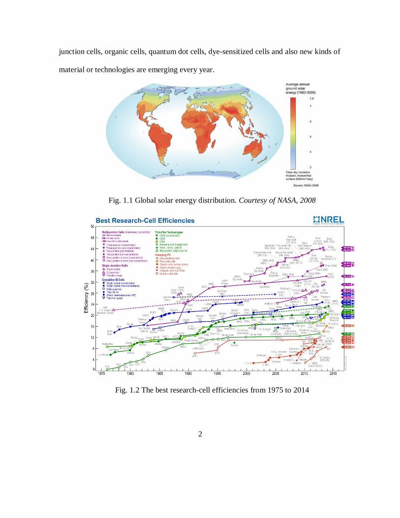
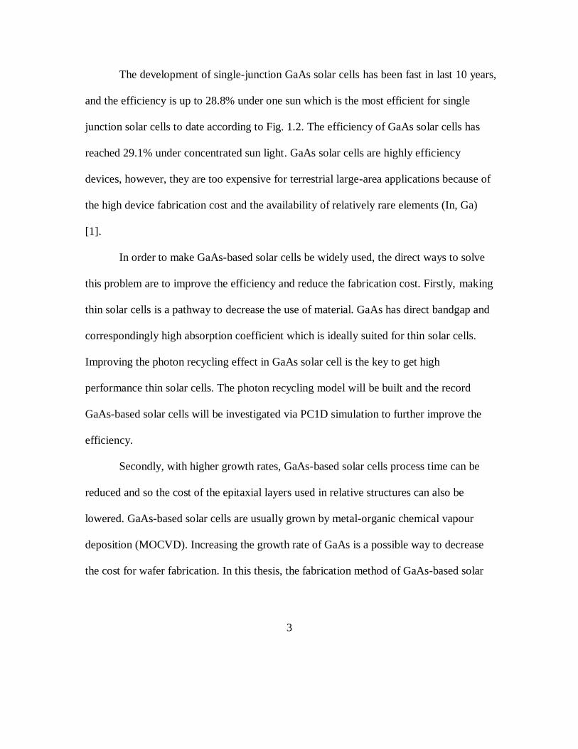
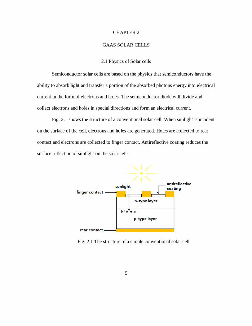
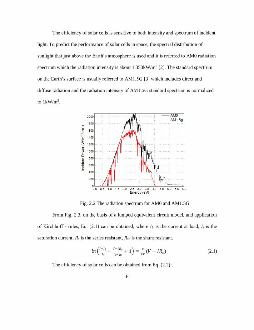
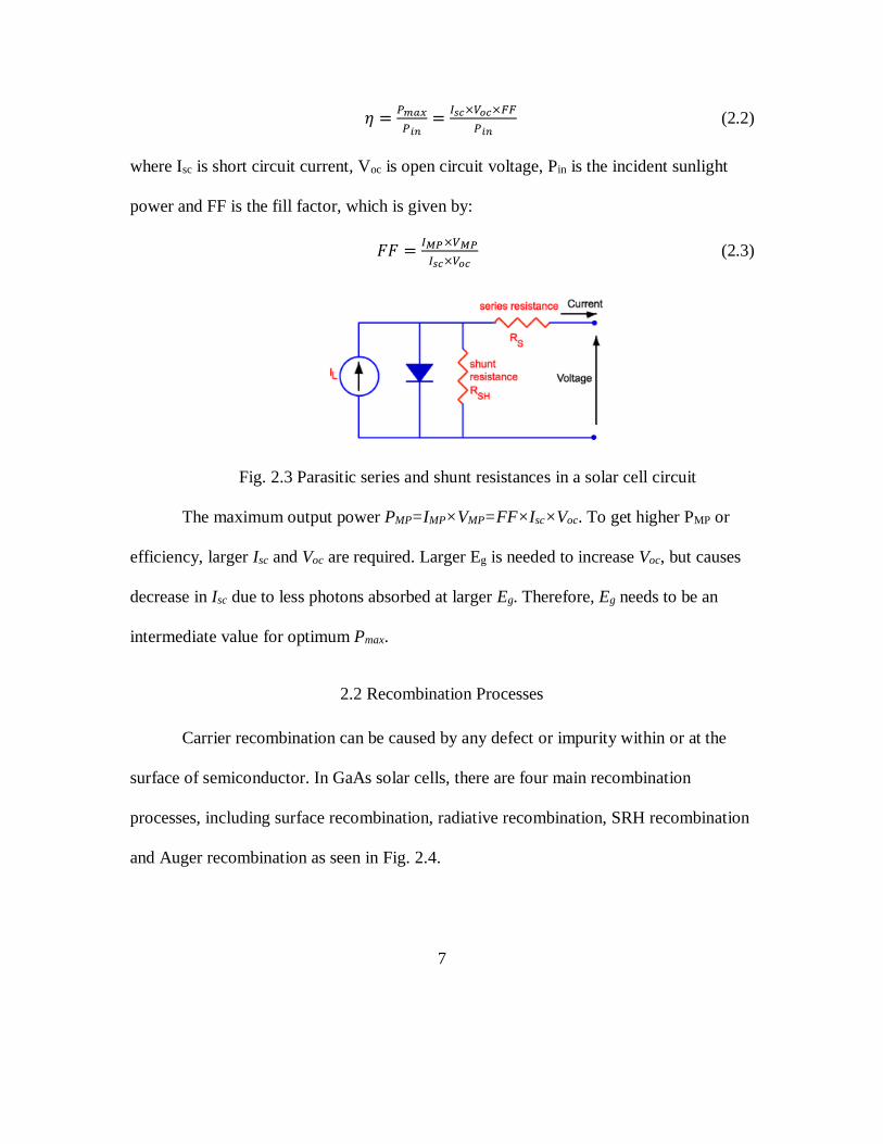
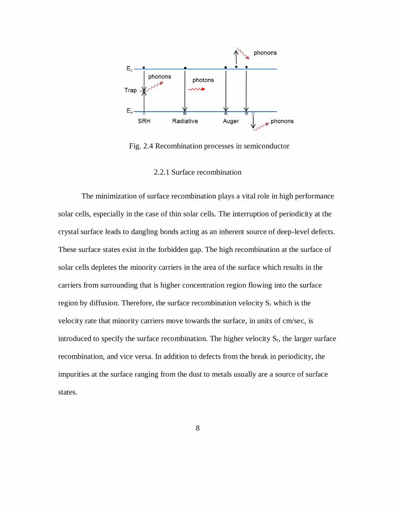
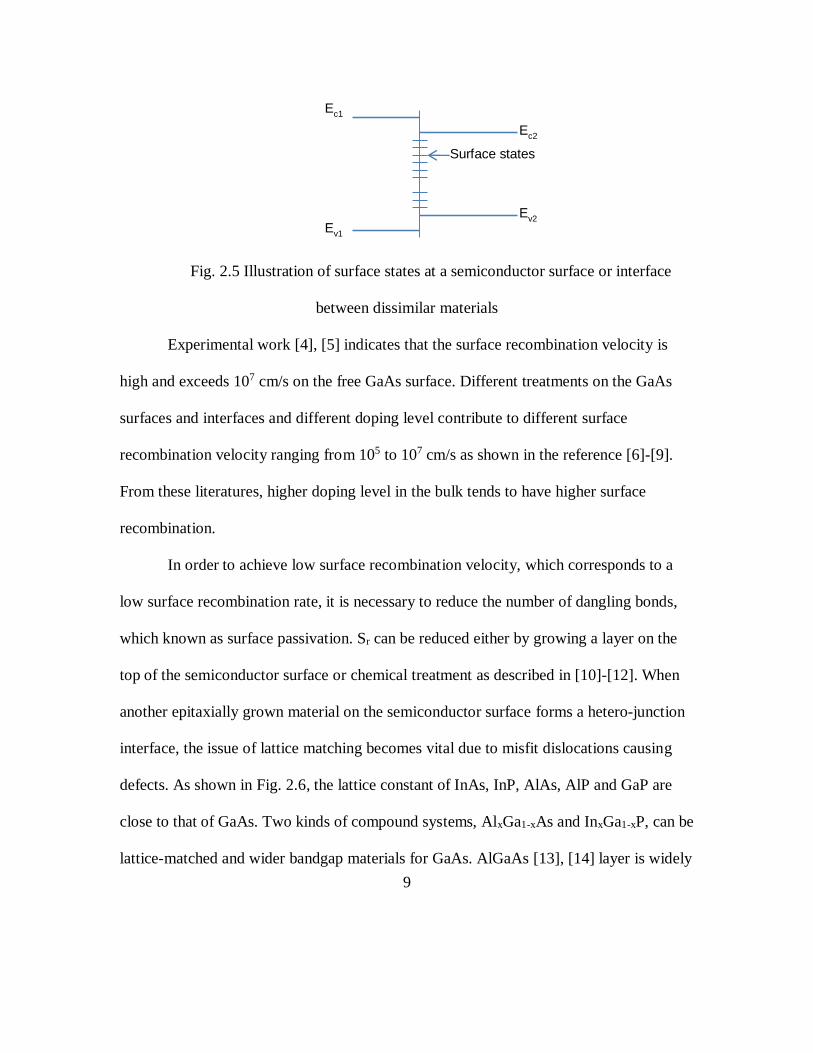
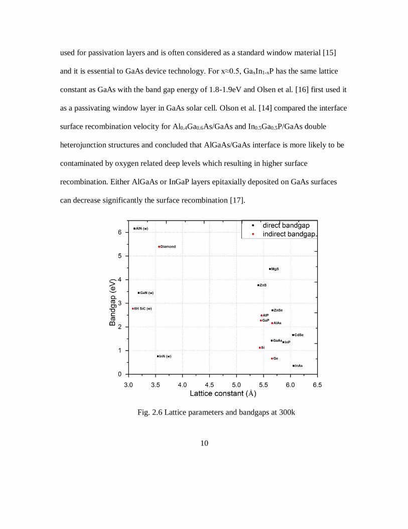
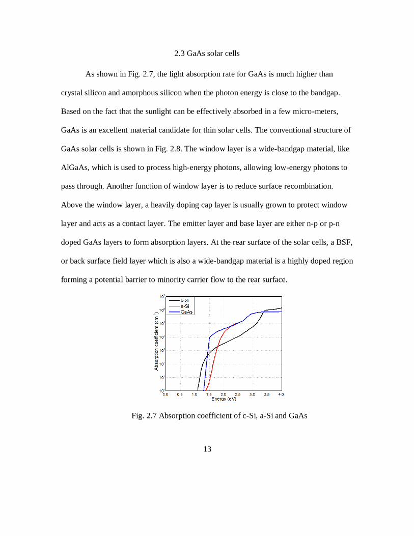
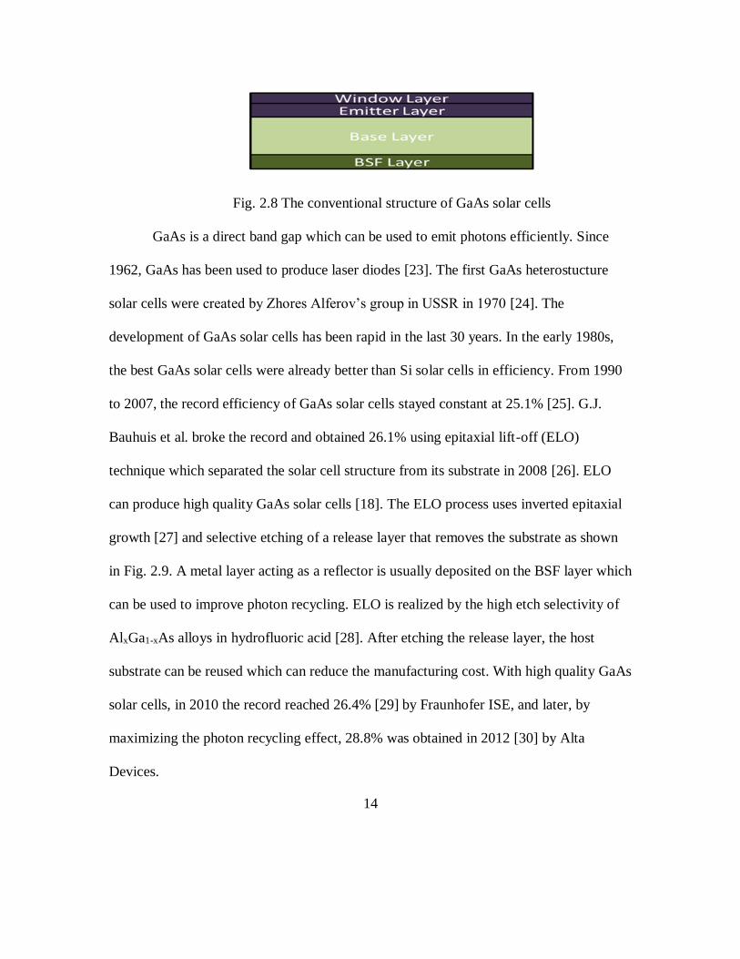
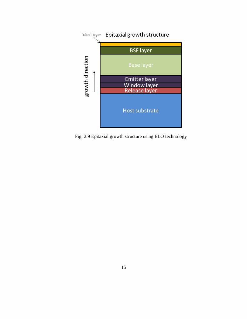
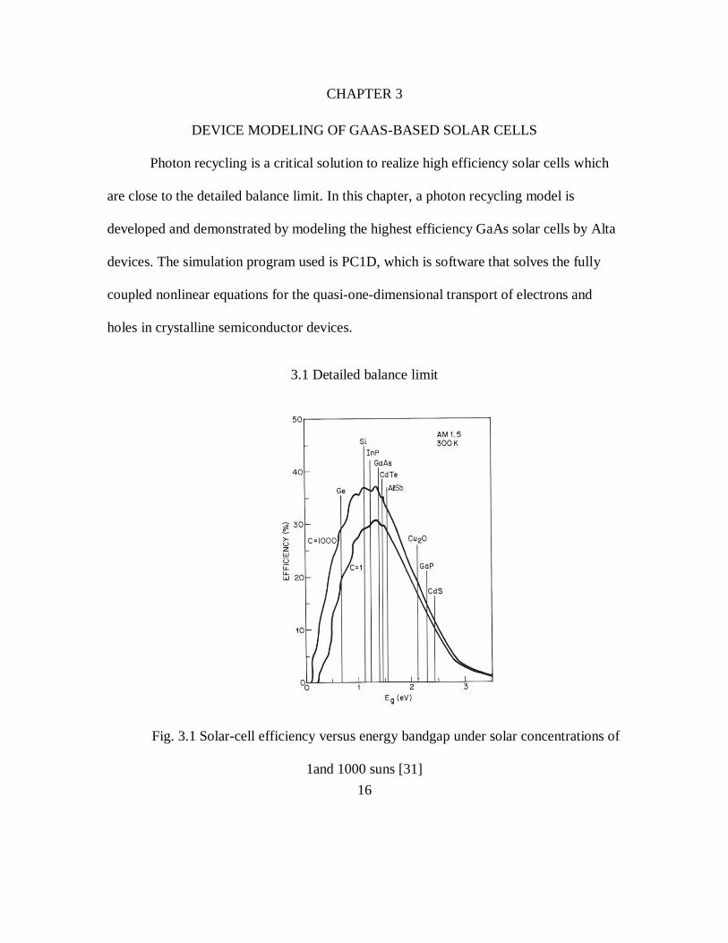
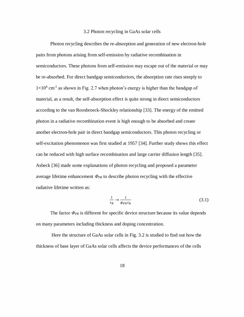
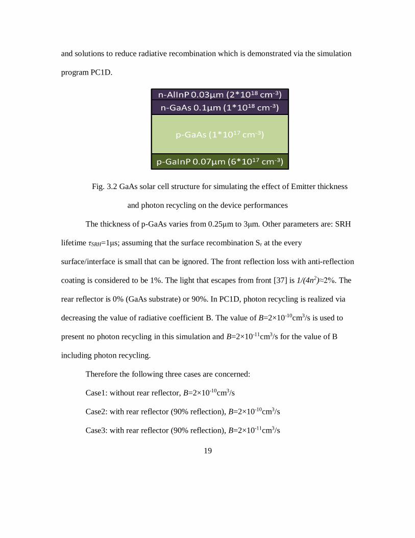
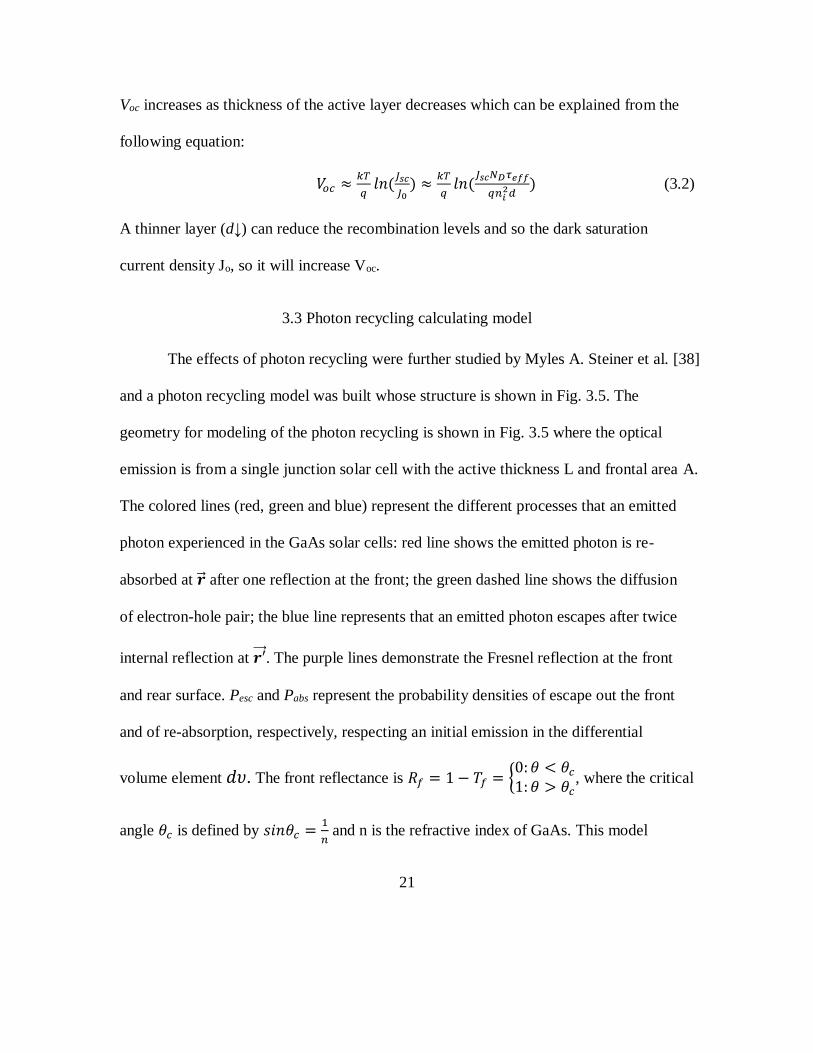
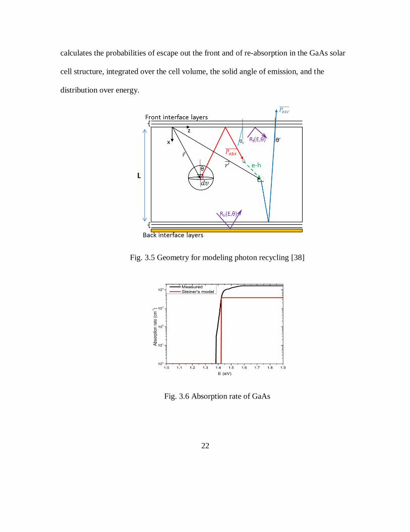
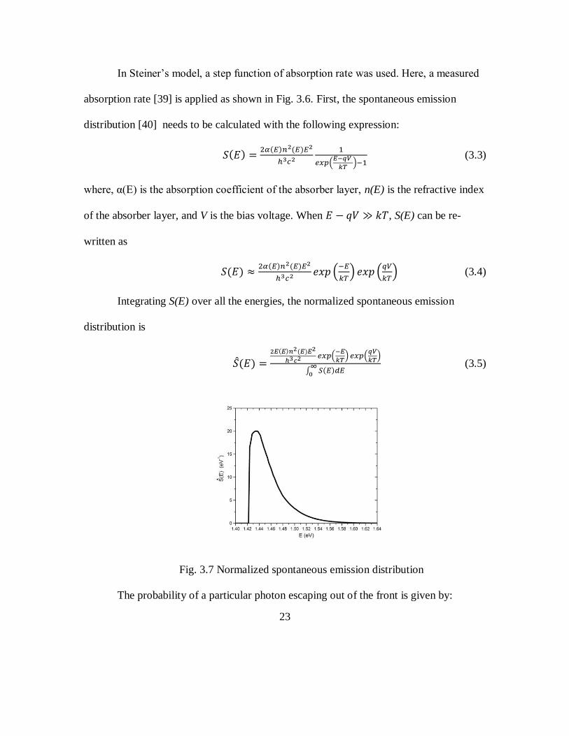
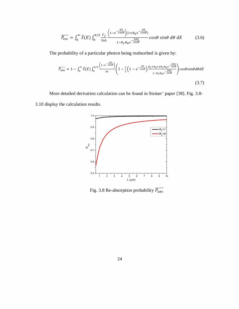
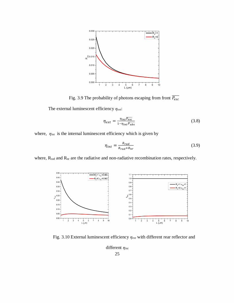
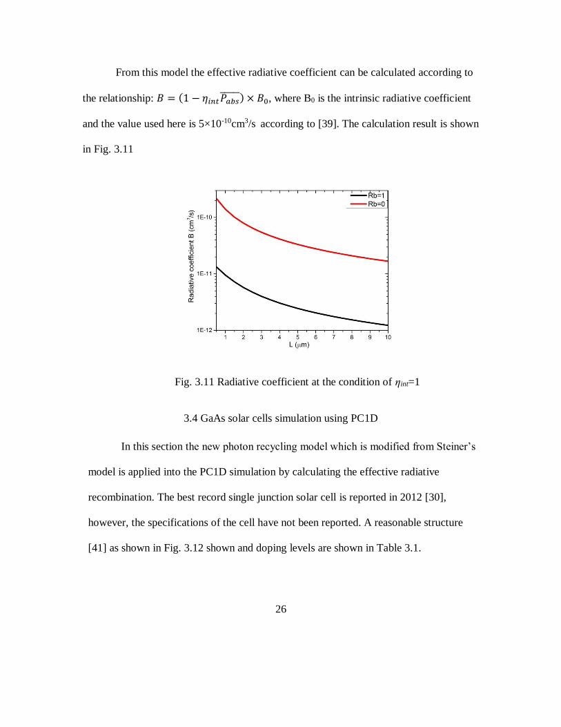
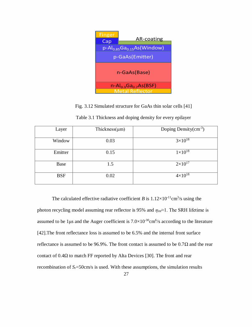
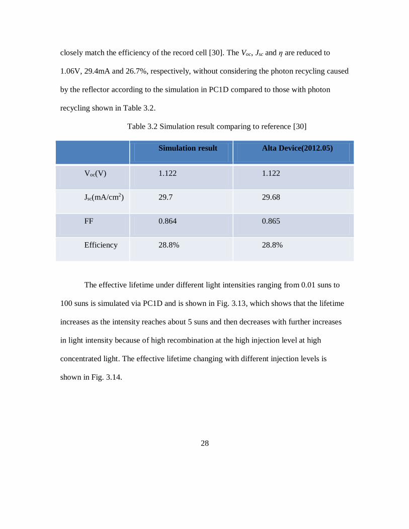
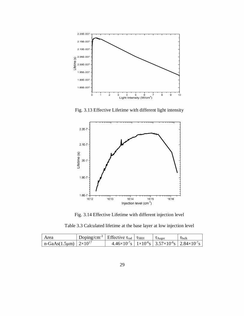
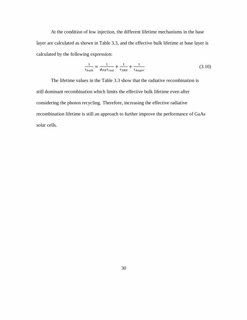
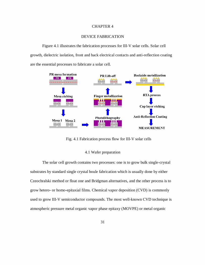
31
CHAPTER 4
DEVICE FABRICATION
Figure 41 illustrates the fabrication processes for III-V solar cells Solar cell
growth dielectric isolation front and back electrical contacts and anti-reflection coating
are the essential processes to fabricate a solar cell
Fig 41 Fabrication process flow for III-V solar cells
41 Wafer preparation
The solar cell growth contains two processes one is to grow bulk single-crystal
substrates by standard single crystal boule fabrication which is usually done by either
Czeochralski method or float one and Bridgman alternatives and the other process is to
grow hetero- or homo-epitaxial films Chemical vapor deposition (CVD) is commonly
used to grow III-V semiconductor compounds The most well-known CVD technique is
atmospheric pressure metal organic vapor phase epitaxy (MOVPE) or metal organic
32
chemical vapor deposition (MOCVD) which is used for mass production due to the
relatively low cost for material growth MOCVD is an epitaxial growth technique in
which the metal-organic precursor gases including dopant species impinge on a wafer
that is placed on a temperature controlled stage resulting in epitaxial growth whose rate
at the order of microns per hour Another epitaxial technique is molecular beam epitaxy
(MBE) whose operation condition requires ultra-high vacuum (UHV) In contrast to
MOCVD for MBE the crystal-growth is performed by physical deposition rather than by
chemical reaction Overall MOCVD is more used because of its relatively low cost and
the monolayer control achievable in the best conditions
Since different lattice constants of the grown layers give rise to strain the lattice
constant is an important hetero-generous growth consideration The strain energy density
increases as deposited layer thickness at the hetero-junction interface and when the
deposited thickness is larger than Matthews-Blakeslee critical thickness limit [43] the
strain energy becomes greater than the bond energy and the total system energy releases
strain potential energy through breaking bonds in the interface One solution to the lattice
misfit problem is to grow relaxed buffer layers which allow the layer to relax and the
dislocation density can be at reasonably low levels
In this thesis the wafers were grown by a commercial company using MOCVD
and the structure is shown in Fig 42 After the wafer fabrication cell isolation and
ohmic contact are two indispensable processes for solar cell fabrication
33
To get rid of particles and contamination wafers are cleaned with the following
steps a) Acetone rinsing for 3 minutes b) Methanol rinsing for 3 minutes c) DI-water
rinsing d) Nitrogen blow-off
Fig 42 The wafer structure of GaAs solar cell grown by MOCVD
42 Mesa etching process
In order to dielectrically isolate solar cells on the wafers mesa etching is needed
As shown in Fig 43 a photolithography for mesa formation is the first step in the mesa
etching process This process was done in the Center for Solid State Electronics (CSSER)
After using spin-coating to form photoresist (AZ4330) coating on wafers using a mask
aligner to photolithography with ultra-violet (UV) and then developing process
(AZ300MIF~50 seconds) mesa patterns were achieved The GaAs layer was etched
using H3PO4H2O2DI water (113) at an etch rate of 25 nms at room temperature and
34
HCl solution etched InGaP layer for 30 seconds as shown in Fig 44 The mesa etching
process is completed when about half of the base layer thickness has been etched
followed by a deionized water rinsing and drying in N2 flow
Fig 43 Illustration of mesa etching process
Fig 44 Selective etch for GaAs-based solar cells
35
43 Metallization
To make a semiconductor device metal contacts have to be made which leads to
metal-to-semiconductor (M-S) contacts The behavior of these junctions depends on the
work functions and the energy band structures of the constituent materials The work
functions of a variety of metals are shown in Table 41 In the electronic contact formed
by metal and semiconductor the Fermi levels will line up by the exchange of charge
carriers across the junction with the consequence that the layers approach the thermal
equilibrium As shown in Fig 45 band bending behavior appears as electrons density
changes and the Schottky barrier height 120601119898is formed at the interface of metal and
semiconductor In order to achieve ohmic behavior and ldquofreerdquo movement of the charge
carriers across the M-S junction the band bending and work function difference should
be reduced Four possible metal-semiconductor junction configurations and the resulting
contact type are shown in Table 42 according to analysis of band bending behavior and
carriers flowing However contact metals may react with or diffuse into semiconductor
surface which leads to the formation of a compound with new electronic properties in the
real condition
Fig 45 Schematic band diagram of a typical Metal-Semiconductor Junction [44]
36
Table 41 Work Functions of Selected Metals [45]
Material Face Work
Function(eV)
Li Polycrystal 29
Na Polycrystal 275
K Polycrystal 23
Rb Polycrystal 216
Cs Polycrystal 214
Al
(1 0 0) 441
(1 1 0) 406
(1 1 1) 424
Ag
(1 0 0) 464
(1 1 0) 452
(1 1 1) 474
Cu
(1 0 0) 459
(1 1 0) 448
(1 1 1) 498
Au
(1 0 0) 547
(1 1 0) 537
(1 1 1) 531
W
(1 0 0) 463
(1 1 0) 525
(1 1 1) 447
Ni
(1 0 0) 522
(1 1 0) 504
(1 1 1) 535
Mo
(1 0 0) 453
(1 1 0) 495
(1 1 1) 455
37
Table 42 Different Possible Metal-Semiconductor Junction Configurations
Junction Configuration Semiconductor Doping Junction type
φMgtφs n-type Schottky
φMltφs n-type Ohmic
φMgtφs p-type Ohmic
φMltφs p-type Schottky
The simple M-S contact theory presented in the previous section assumes that the
electron affinities and work functions remain unchanged when the contact is made
However the assumption is not true after considering the surface states at the metal-
semiconductor interface [46] In the reference [47]-[52] some theories and various
mechanisms including electronegativeity have been developed but no precise definite
explanation has been made to explain the properties of metal and compound
semiconductor contacts likely due to the lack of detailed information on the nature of M-
S contacts on the atomic level and differences in deposition techniques for contact In
order to obtain ohmic contact for GaAs and other compound semiconductors all
electronic states should be filled or emptied [46] There are two ways to accomplish this
one is heavily doping the semiconductor layer and the other one is diffusing metal from
metal into semiconductor Therefore thermal processing of metallic layers like
annealing is a crucial process A cap layer is needed to protect the epitaxial layers from
being damaged by the deep diffusion of metals Generally a heavily doped cap layer will
38
be applied to achieve good ohmic contact The following metallization for n- and p-type
was completed in the clean room of Solid State Electronics Research Center (CSSER) at
ASU
431 n-type Front metallization
The metals stack and layers thicknesses of the multilayer metallization for ohmic
contact were selected according to literatures GeAuNiAu layers are chosen to be
deposited on n-type front to form ohmic contact [46]
The following steps are for finger metallization are a) Photoresist (AZ4330)
coating using a spinner b) Photolithography using a mask aligner c) Developing process
(AZ300MIF ~50 sec) N-contact metal deposition using a thermal evaporator
GeAuNiAu (2605401501500Å) and lift-off process using Acetone are two processes
to achieve finger metallization (n-type ohmic contact)
Fig 46 Illustration of n-type front metallization
39
432 p-type Backside metallization
The TiPtAu [54] system is commonly used for p-type rear ohmic contacts GaAs
surfaces tend to lose arsenic during contact formation and thus a diffusion barrier like Ti
or Ni is often used to reduce As loss
Using a photo resist (AZ4300) coating on the front to protect finger TiPtAu
(40101500Å) is deposited using E-beam evaporator After removing the photo resist
using Acetone the backside metallization is completed
Fig 47 Illustration of p-type backside metallization
40
433 Rapid Thermal Annealing (RTA)
After depositing metals on the front and rear side of solar cells rapid thermal
annealing (RTA) is required for achieving ohmic contact The I-V curve of the surface
shown in Fig 48 is called double Schottky diodes behavior
Fig 48 I-V curve of surface contact without RTA process showing non-ohmic
behaviors
Transmission line measurements (TLM) which were originally proposed by
Shockley [55] to determine specific-contact resistivity are used to find optimized
annealing temperature and annealing time so that minimum contact resistance of solar
cells can be achieved
41
Fig 49 Schematic transmission line measurement
As shown in Fig 49 TLM measurements are performed by a probe station with a
parameter analyzer like HP4145 after metals are patterned and annealed by different
recipes A voltage between several pairs of adjacent pads in a row is applied and the I-V
curves are measured The design of TLM patterns requires all the pads in one row the
pads are the same size and the distance between pads is varied Figure 410 shows the
TLM patterns used in this experiment
Fig 410 The structure of TLM patterns used in the experiment
The resistances between two pads are calculated by R=VI which is a total
resistance Rtotal=2Rc+Rsemi where Rc is contact resistance and Rsemi is the semiconductor
resistance By measuring of the resistance between metal pads for a set of different gaps
42
the total resistance according to the contact separation is plotted in Fig 411 After the
linear fitting of Rtotal vs contact separation sheet resistance of semiconductor can be
obtained by equation Rsheet=slopetimesw where w is the width of pattern which is shown in
Fig 49 and contact resistance can be got from equation Rc=05timesintercept The specific
contact resistivity can be calculated by ρc=RctimesA where A is the contact pad area
Fig 411 The total resistance at different pad positions of one pattern and linear
fitting
Fig 412 The schematic of TLM patterns with and without mesa etching
As shown in Fig 412 the TLM pattern with mesa etching has better uniformity
in current flow In this optimization process the patterns do not have mesa etching
43
process leading to the result with some noise In order to certify almost the same
conditions the same wafer and same depositing process are used in comparing annealing
temperature varying from 320-380 380-440 for 20s and annealing time from 20s to
50s at 380 From Fig 413 the specific contact resistivity seems not to have big
difference at the annealing time from 360-440 for 20s In addition to changing RTA
temperatures different annealing times of 20s and 50s at a fixed RTA temperature of 380
is compared as shown in Fig 414 These results show longer annealing times have lower
contact resistivity Therefore an RTA temperature of 380 for 50s is an optimum
condition among these different conditions for n-type ohmic contact
Fig 413 The specific contact resistivity at different annealing temperature for 20s
(two row patterns are measured)
44
Fig 414 The specific contact resistivity with different annealing time at the RTA
temperature of 380 (two row patterns are measured)
The front n-type contact is studied in the previous section Here different
annealing temperatures are compared for p-type contact using TLM as shown in Fig 415
that 380 for 50s is better than 400 for 50s Therefore the RTA condition for n-type
and p-type contact of the wafers used in this thesis is 380 for 50s All the RTA
processing was done in the Solar Power Lab of ASU
Fig 415 p-type contact results of TLM
45
44 Cap layer etching
The top GaAs cap layer is heavily doped and there are two functions for the cap
layer on the window layer one is to protect a window layer and the other is to be used for
electric contact layer After finishing ohmic contacts for front and rear side the EQE
spectra are shown in Fig 416 where the light with short wavelengths is absorbed at a
cap layer Therefore the cap layer needs to be etched out from a window layer using
H3PO4 H2O2 DI water (113) for ~10s which was completed in Solar Power Lab
Fig 416 The EQE spectra with and without a cap layer
46
45 Anti-reflection coating (ARC)
Fig 417 The structure of ARC on GaAs
Reducing the optical losses is a key to achieving high efficiency solar cells The
reflection on the GaAs solar cells without antireflection coatings is very high more than
30 according to the equation [56] 119877 = (1198991minus1198990
1198991+1198990)2 It is not sufficiently effective to have
a single layer coating for GaAs solar cells because the single layer coating only can
effectively reduce the reflection in a narrow wavelength range In other words the single
layer just can realize the minimization of one wavelength Two or more anti-reflection
coating layers are generally required to get better transmittance An alternative is a
graded-index coating which the refractive indices increase from small to large from the
air Therefore double layers antireflection coatings (DLARC) which contain low and
high refractive indices are necessary to get further reflectivity decrease
There are two advantages to deposit two layers rather than single layer first two
reflection minima can be achieved which helps to lower the average spectral-weighted
reflection rate second the optical performance is less sensitive to the thickness variations
[57] The most popular DLARC in GaAs based solar cells are zinc sulfide
47
(ZnS)magnesium fluoride (MgF2)
Considering normal incidence of light the surface reflection at a specific
wavelength can be minimized when the refractive indexes meet the following relation
1198990
1198991=
1198991
1198992=
1198992
1198993 (41)
The refractive index of GaAs is 382 at a wavelength of 650nm [58] The value of
n3 is 382 therefore the optimized n1 is 156 and n2 is 244 as calculated through
Equation 41
The reflection of DLARC can be calculated through the equations below
119903119894 =119899119894minus1minus119899119894
119899119894minus1+119899119894 where i=123 (42)
120579119895 =2120587119899119895119905119895
120582 where j=12 (43)
119877 =
sum 1199031198942+prod 119903119894
2+211990311199032(1+11990332)11988811990011990421205791+211990321199033(1+1199031
2)11988811990011990421205792+2119903111990331198881199001199042(1205791+1205792)+211990311199032211990331198881199001199042(1205791minus1205792)
31
31
1+119903121199032
2+119903121199033
2+119903221199033
2+211990311199032(1+11990332)11988811990011990421205791+211990321199033(1+1199031
2)11988811990011990421205792+2119903111990331198881199001199042(1205791+1205792)+211990311199032211990331198881199001199042(1205791minus1205792)
(44)
where n0 is the refractive index of the surrounding region n1 is the refractive
index of the first layer of ARC and t1 is the thickness n2 is the refractive index of the
second layer of ARC and t2 is the thickness
To calculate the optimized combinations of refractive indexes and thicknesses for
the incident spectrum the average weighted reflection should be calculated using the
equation [59] below
119877119908 =int 119877(120582)119873119901ℎ(120582) 119889120582120582119898119886119909120582119898119894119899
int 119873119901ℎ(120582) 119889120582120582119898119886119909120582119898119894119899
(45)
48
where R(λ) is the wavelength-dependent reflection Nph(λ) is the photon flux of the
AM15 (or AM0 for space use) solar spectrum as a function of the wavelength
Suitable materials with low refractive index around 156 are SiO2 Al2O3 and
MgF2 and the materials with high refractive index around 244 are ZrO2 ZnS and TiO2
All refractive index data is from [58]The minimum Rw is achieved in the range of 300 -
900 nm as shown in Table 43 The minimum Rw of SiO2TiO2 layers for DLARC is as
low as 123 therefore these two materials are further studied in this thesis
In this thesis the DLARC SiO2TiO2 films are deposited by e-beam evaporator in
CSSER The refractive index of SiO2 and TiO2 deposited by E-beam evaporator is
affected significantly by the deposition conditions [60]-[62] such that to a certain degree
the higher vacuum in the chamber the higher substrate temperature of the substrate and
the faster growth rate the higher refractive index can be obtained Through some
experiments the refractive index of SiO2 is approximately 145 and that of TiO2 is
ranges from 22 to 24
49
Table 43 Simulation results using different material groups
ARC Layer1 ARC Layer2 Optimum
Thicknessnm
Theoretical
Refractive
Indices
(λ=650nm)
156 244 Layer1 Layer2 minimization
of Rw
Suitable
materials
(λ=650nm)
SiO2(n=154) ZrO2(n=2205) 66 51 307
SiO2(n=154) ZnS(n=255) 85 51 121
SiO2(n=154) TiO2(n=257) 85 51 123
Al2O3(n=1658) ZrO2(n=2205) 57 45 379
Al2O3(n=1658) ZnS(n=255) 75 46 21
Al2O3(n=1658) TiO2(n=257) 76 46 202
MgF2(n=1377) ZrO2(n=2205) 89 60 202
MgF2(n=1377) ZnS(n=255) 98 54 124
MgF2(n=1377) TiO2(n=257) 98 54 128
50
On a GaAs substrate 50nm TiO2 under the conditions of 55times10-5Torr vacuum
deposition rate of 006nms and substrate temperature of 300 and 90nm SiO2 under the
conditions of 48times10-7Torr vacuum deposition rate of 01nms and substrate temperature
of 78 are deposited using an E-beam evaporator A weighted reflection of 19 at a
wavelength range from 400-900nm is achieved in contrast to that of 297 without
antireflective coating as shown in Fig 418
Fig 418 The reflection spectra with and without ARC on GaAs wafers
Considering that 300 for more than 1 hour may damage GaAs based solar cells
for the final solar cell fabrication anti-reflection coatings were deposited at room
temperature rather than 300 and the result will be shown in Chapter 5
51
CHAPTER 5
MATERIAL CHARACTERIZATION
In this chapter two kinds of GaAs wafers with different growth rates grown by
MOCVD are compared (Fig 51) from a commercial company The slow growth rate is
14μmhour and fast growth rate is 55μmhour Two wafers are prepared for slow growth
(slow-1 and slow-2) and fast growth (fast-1 and fast-2)
Fig 51 The structure of GaAs solar cell wafers grown by MOCVD
51 Crystalline Quality
The as-grown samples are characterized by high-resolution X-ray diffraction
(HRXRD) to determine layer composition strain and crystalline quality X-ray is well
suited for analyzing epitaxial thin sloar cells deposited on single-crystal substrates
because the wavelength of X-ray is comparable with the inter spacing (10-8cm) in crystals
52
The X-ray rocking curve which is the plot of X-ray intensity against the X-ray incident
angle Omega is taken from two cuts of the Ewald sphere [63] in the reciprocal space as
shown in Fig 52 In Fig 52 hkl is the Miller indices of the plane on the crystal and s is
the diffraction vector GaAs and InGaP both have the zinc blend crystal structure When
the diffracted angle 2θ=6605 deg with copper X-ray source according to Braggrsquos law
λ=2dhklsinθ and intensity calculation from structure factor the X-ray beam hits on the
(004) planes of GaAs can produce the highest diffraction peak Therefore the diffraction
measurement is in the vicinity of (004) planes
Fig 52 Schematic Ewaldrsquos sphere construction applied in XRD measurement
53
Fig 53 Schematic double-crystal (DC) rocking curves (RC) measurement
Figure 54 Schematic triple-crystal (TC) rocking curves (RC) measurement
There are two instrumental configurations for HRXRD double-crystal and triple-
crystal rocking curves measurement as shown in Fig 53 and Fig 54 respectively The
54
XRD measurement was done in LeRoy Eyring Center for Solid State Science In double-
crystal rocking curves measurements the sample is rotated about its omega axis changing
the incident angle and all Bragg angles are measured simultaneously over a limited range
so more peaks are observed The analyzer constrains the detector and only one special
peak is observed in triple-crystal rocking curves measurement
Fig 55 Double-crystal (DC) -2 rocking curves (RC) of Sample slow-1 in the
vicinity of (004) reflection (Bluendash Experimental Red ndash Calculated)
From the rocking curves the peak position can give the d-spacing for the Bragg
peak which will provide the information on anything that changes the lattice parameter of
the unit cell such as composition or strainrelaxation The width of the epitaxial filmrsquos
Bragg peak can be used to quantify the film thickness and the thickness fringes can also
be used to quantify the film thickness From the double-crystal rocking curve and doing
55
calculations as shown in Fig 55 the different layer thickness and composition (from
substrate to top layers) of Sample slow-1 can be achieved
Substrate thick = 60000 m GaAs (0 0 1) Strain = 00
Layer 1 thick = 00040 m Ga0495In0505As02P08 Strain = 8382ppm R = 00
Layer 2 thick = 01060 m Ga04975In05025P Strain = 1241ppm R = 00
Layer 3 thick = 00020 m GaAs08P02 Strain = -7188ppm R = 00
Layer 4 thick = 3200 m GaAs Strain = 0ppm R = 00
Layer 5 thick = 00040 m Ga0495In0505As02P08 Strain = 8382ppm R = 00
Layer 6 thick = 00530 m Ga04995In05005P Strain = 1093ppm R = 00
Layer 7 thick = 000200 m GaAs08P02 Strain = -7188ppm R = 00
Layer 8 thick = 01920 m GaAs Strain = 0ppm R = 00
From the double crystal (DC) rocking curves (RCs) in Fig 56 the highest peaks
come from GaAs layers and the second highest peaks are from InGaP layers The
different positions of InGaP peak indicate the different indium composition in InGaP
layers The indium composition strain and epi-thickness in InGaP layers are calculated
and displayed in Table 51 The different thicknesses may be due to the stage temperature
variations during the wafer growing process using MOCVD
56
Fig 56 Double-crystal (DC) -2 rocking curves (RC) in the vicinity of (004)
reflection (Bluendash slow-1 Redndash fast-1 Greenndash slow-2 and Violetndash fast-2)
Table 51 Indium composition strain and epi-thickness from the DC rocking
curves
Sample In () Strain (ppm) Thickness (nm)
slow-1 5005 1093 53
fast-1 4955 723 555
slow-2 497 834 56
fast-2 5022 1219 585
57
Fig 57 Triple-crystal (TC) rocking curves (RC) of Sample slow-1 (Bluendash
Substrate peak (004) Reflection Redndash GaInP peak)
Fig 58 TC rocking curves (RC) of Sample slow-1(red) and Sample fast-
1(blue) at InGaP peak
58
Fig 59 TC rocking curves (RC) of Sample slow-2 (blue) and Sample fast-2
(red) at InGaP peak
Calculating the full width at half maximum (FWHM) of peaks is a path to
estimate defects in crystals A perfect crystal will produce a very sharp peak with an
intrinsic width Defects such as dislocation cause peak broadening at the Bragg angles
Dislocations are lines along which the crystal pattern is broken in single crystals But in
general dislocations appear in curves or loops which in three dimensions form and
interlocking dislocation network In Fig 57 the TC rocking curve of Sample slow-1 is
compared to that of substrate The density of primary dislocation loops (DLs) in Sample
slow-1 104cm2 and in Sample fast-1 it is about 4 ndash 64 times 104cm2 from Fig58 The
more intense wide diffuse base on Sample fast-1 RC suggests more secondary DLs in the
volume of InGaP layer(s) From Fig 59 the density of DLs in Sample slow-2 is not
more than 35 times 104cm2 and in Sample fast-2 it is about 15 times 104cm2
59
Table 52 The DLs for solar cell wafers grown at different growth rates
Sample Density of Dislocation Semi-Loops
slow-1 104cm2
fast-1 4 ndash 64 times 104cm2
slow-2 35 times 104cm2
fast-2 15 times 104cm2
Therefore from Table 52 the density of DLs for these slow and fast growth
wafers is on the same level The crystal quality of the fast growth wafers is not degraded
from XRD analysis
52 Solar cell characterization
The as-grown wafers are fabricated into solar cells using the processes described
in Chapter 4 The size of the fabricated solar cells is 05cmtimes05cm The optical and
electrical properties of the fabricated solar cells of Sample slow-2 (slow growth) and
Sample fast-2 (fast growth) are compared Surface reflection EQE dark current and
Suns-Voc were measured in the Solar Power Lab
521 Surface reflection
The surface reflection of the solar cells affects the intensity of the incoming light
beam that gets into cells 56nm TiO2 and 90nm SiO2 are deposited onto the GaAs solar
60
cells surface by E-beam evaporator at room temperature As shown in Fig 510 the
surface reflection is quite high without anti-reflective coating (ARC) whose weighted
reflection is more than 33 The reflection on the cells is about 8 which contains the
reflection of fingers on the surface From the reflection curves the conclusion can be
made that there is no big difference between the slow and fast growth solar cells and
some slight difference may be caused by a little difference of layer thickness and indium
composition Therefore nearly the same surface reflection for both cells is confirmed
Fig 510 Surface reflection spectra
Table 53 The weighted reflection Rw in the wavelength region of 300-900nm
Before ARC After ARC
slow fast slow fast
3356 3387 82 81
61
522 External quantum efficiency (EQE)
The external quantum efficiency (EQE) is the ratio of the number of carriers
collected by the solar cell and to the number of photons from a given light incident on the
solar cell EQE at each wavelength of the light is defined by
119864119876119864 =119890119897119890119888119905119903119900119899119904119904119890119888119900119899119889
119901ℎ119900119905119900119899119904119904119890119888119900119899119889=
1240119899119898119890119881times(119869119897119894119892ℎ119905minus119869119889119886119903119896)
120582times119875119897119894119892ℎ119905 (51)
There is some difference between 600nm to 880nm for slow growth and fast
growth solar cells as shown in Fig 511
Fig 511 EQE spectra of the slow and fast growth cells
The average EQE can be calculated by using the following equation
119864119876119864119886119907119892 =int 119864119876119864(120582)119873119901ℎ(120582)ⅆ120582120582max120582min
int 119873119901ℎ(120582)ⅆ120582120582max120582min
(52)
From the EQE spectra Jsc can be estimated by
62
119869119904119888 = 119902 lowast int 119864119876119864(120582)119873119901ℎ(120582) 119889120582120582119898119886119909
120582119898119894119899 (53)
As shown in Table 54 both average EQE and the solar cell with fast growth are
lower than those of the slow growth solar cell
Table 54 The average EQE and estimated Jsc for the slow and fast growth cells
slow growth fast growth
EQEavg Jsc(mAcm2) EQEavg Jsc(mAcm2)
without ARC 5430 183 5173 174
with ARC 7055 237 6742 227
In order to investigate the cause for EQE difference in the wavelength region
between 600nm and 880nm some PC1D simulations are carried out The radiative
lifetime in the base layer is assumed to be 05μs corresponding to a radiative coefficient
of 20times1010cm-3s From the simulation results shown in Fig 512-513 when the
thickness of base layer decreases and the SRH lifetime decreases in the base layer the
EQE decreases in the wavelength range of 600-880nm The reason why fast growth cells
have lower EQE in the wavelength range of 600nm-900nm may be due to lower SRH
lifetime caused by increased crystalline defects The surfaceinterface recombination
difference may be also a reason for different EQE More discussion will be carried out
after analyzing the I-V data under 15AM spectrum
63
Fig 512 EQE spectra for base layer with different thickness
Fig 513 EQE spectra for base layer with different SRH lifetime
64
523 Dark current
The dark I-V is measured to examine the diode rectifying properties under dark
condition In the dark solar cells are working as a large flat diode and the I-V curves
show exponential behaviors with the applied voltage as seen in Fig 514(a)
(a) Dark I-V on a linear scale (b) Dark I-V on a semilog scale
Fig 514 Dark current
The dark saturation current J0 and ideality factor n are obtained by the following
equation
119897119899(119869) = 119897119899(1198690) + (119902
119899119896119879)119881 (54)
where J is the dark current density kTq is the thermal voltage and V is the bias voltage
The calculated results are listed in Table 55 where the ideality factor of slow growth is
slightly larger than that of fast growth and also for J0
65
Table 55 Diode parameters of the cells from the linear fitting and calculation
from dark I-V
Slow growth Fast growth
Intercept -19685 -20865
J0(Acm2) 28times10-9 87times10-10
Slope 113655 116146
Ideality factor 340 333
524 Suns-Voc
The Suns-Voc [64] is a measurement that directly measures Voc as a function of the
light intensity typically measured ranging from a few suns to just below 01 suns as
shown in Fig 515 In contrast to dark I-V measurement the suns-Voc follow the dark
current curve but it has no effects of series resistance The local ideality factor m can be
derived from the following equation [65]
119904119906119899119904 ∙ 119869119904119888 = 1198690119890119909119901(119902119881119900119888
119898119896119879) (55)
where suns is the light intensity Jsc is the short circuit current density of the cell
at one sun and J0 is the dark saturation current density
66
Fig 515 Suns-Voc curves against Voc on a semilog scale
Table 56 Ideality factors calculated from Suns-Voc curves
Slow growth Fast growth
intercept -1462 -1801
slope 16158 1904955
Ideality factor 239 203
From Table 56 local ideality factor of slow growth cell is larger than that of fast
growth cell which is consistent with the calculated result from the dark I-V data
525 I-V under AM15 spectrum
The measurement of the conversion efficiency of solar cells is a fundamental
characterization technique for solar cells The solar simulator whose lamp is simulating
air mass 15 spectrum (AM15) with the illumination intensity of 100mWcm2 is
67
employed to simulate standard sun light on earth surface The cells are measured at room
temperature and the I-V curves shown in Fig 516 The Jsc increases significantly after
anti-reflective coating and Voc slightly increases
Fig 516 I-V curves of slow growth and fast growth
The shunt resistance and series resistance can be estimated [66] from the I-V
curves by calculating Rsh=dVdI at V=0 and Rs=dVdI at I=0 The TLM patterns on the
wafers are measured to extract the sheet resistance and specific contact resistivity in Fig
517 The sheet resistance of the slow growth wafer is slightly lower than that of fast
growth wafer and the specific contact resistivity for both wafers is almost same in this
study
68
Fig 517 Sheet resistance (Rsheet) and specific contact resistivity (ρc) measured
from the TLM patterns on the surface of solar cells (a b and c indicate three patterns at
different positions of the wafers)
From Table 57 the fill factors of the cells of slow growth and fast growth are
close and both are about 80 The internally measured efficiency of both cells is above
17 The shunt resistance Rsh and series resistance Rs are also shown in Table 57 where
the calculation is based on the linear simulation to get slope at the V=0 and J=0
respectively The current density Jsc of the slow growth cell is higher than that of the fast
growth cell while the open circuit voltage of the fast growth cell is higher than that of
slow growth cell As shown in the simulation result of Fig 33 the thinner base layer the
higher Voc and the lower Jsc can be obtained The simulation of the structure shown in Fig
51 result shows that if the lifetime goes to 5ns and 1ns without considering the interface
recombination the open circuit voltage is 09611V and 09111V respectively simulated
by PC1D Therefore the base thickness of fast growth solar cells may not be well
69
calibrated orand there is large interface recombination that cannot be ignored Lifetime
measurement is needed to further investigate the difference between fast and slow growth
solar cells
Table 57 Device performances of the slow and fast growth cells
Slow growth
(wo ARC)
Slow growth
(w ARC)
Fast growth
(wo ARC)
Fast growth
(w ARC)
JscmAcm-2 187 235 177 231
VocV 0923 0926 0941 0947
FF 792 790 815 800
Efficiency 1365 172 1359 175
Rsh(Ω-cm2) 29412 54437 83333 37369
Rs(Ω-cm2) 30 24 26 30
70
CHAPTER 6
CONCLUSION
61 Summary
In this thesis the different recombination mechanisms such as surface
recombination radiative recombination and non-radiative recombination are described
The effect of photon recycling in GaAs solar cells is studied via building a photon
recycling model and PC1D simulation The photon recycling plays a vital role in
approaching the detail balance limit The model of photon recycling is built by modifying
the Steinerrsquos model This model is successfully applied to the simulation of the world
record single-junction GaAs solar cell by assuming some boundary conditions In
addition the effect of the base layer thickness is discussed the less thickness of GaAs
solar cells in the case of low surface recombination the higher Voc can be achieved In
the thin GaAs-based solar cells with a good mirror at the rear side high Voc can be
obtained without sacrificing Jsc benefited from the light trapping and photon recycling
The fabrication processes of GaAs solar cells are described as the following steps
wafer fabrication dielectric isolation front and rear side metallization RTA cap layer
etching and anti-reflective coating In order to achieve good ohmic contacts for GaAs
solar cells transmission line method (TLM) was used to optimize the annealing time and
temperature Some ARC simulation of different material groups using Matlab showed
ARC effects on the surface reflection of GaAs materials The double crystal anti-
reflective coating (DLARC) of SiO2TiO2 shows good anti-reflective effect in the
71
simulation nevertheless the refractive index of SiO2 and TiO2 especially for TiO2 is
sensitive to the deposition conditions such as chamber vacuum substrate temperature and
deposition rate
To corroborate the modeling results studied here two kinds of wafers grown at
different growth rates of 14 μmhour and 55 μmhour by MOCVD are investigated in this
work By analyzing the device performances of the fabricated solar cells the crystalline
quality of the fast and slow growth rate do not show big difference confirmed by XRD
measurements The device performances of EQE dark-current suns-Voc and I-V under 1
sun were measured to compare the electrical properties of these two solar cell wafers
The EQEavg Voc Jsc FF and efficiency of the slow and fast growth cells with ARC are
70556742 09260947V 235231mA 079080 172175 respectively The
different Voc and Jsc between the two cells may be due to the difference of the bulk
lifetime in the base layer orand the interface recombination through PC1D simulation
nevertheless the exact reasons need to be further investigated
62 Future work
The thicknesses of the ohmic metallization for n-type and p-type contact have not
been calibrated and thus the calibration should be done to obtain higher fill factor The
ARC without heating the substrate is needed to be redesigned to achieve better ARC
effect In order to identify the reason for the difference in the device performances of the
two different cells the thickness of every epi-layer is necessary to be calibrated The
minority carrier lifetime of the fast and slow growth cells is also needed to be measured
72
and compared because it is one of the key factors determining the cell performances In
this work the Voc obtained after fabrication is much lower than theoretical value which is
more than 1V and the reasons needs to be investigated in order to further improve GaAs
solar cells performance
73
REFERENCES
[1] G Phipps C Mikolajczak and Terry Guckes ldquoIndium and Gallium long-term
supplyrdquo Renewable Energy Focus Vol 9 pp 56 58-59 Jul-Aug 2008
[2] JL Gray ldquoThe Physics of the Solar Cellrdquo in Handbook of Photovoltaic Science
and Engineering2nd ed A Luque and S Hegedus Ed John Wiley amp Sons 2011pp 82-
129
[3] ASTM G173-03 ldquoStandard tables for reference solar spectral irradiances Direct
normal and hemispherical on 37deg tilted surfacerdquo ASTM International (2003)
[4] H C Casey and E Buehler ldquoEvidence for low surface recombination velocity on
n-type InPrdquo Applied Physics Letter Vol 30 pp 247 1977
[5] A Ehrhardt W Wettling and A Bett rdquoTransient photoluminescence decay study
of minority carrier lifetime in GaAs heteroface solar cell structuresrdquo Applied Physics
A Vol 53 pp 123-129 Aug 1991
[6] NL Dmitruk VI Lyashenko AK Tereshenko and SA Spektor ldquoInvestigation
of surface recombination on epitaxial GaAs filmsrdquo Physics Status Solidi (A) Vol 20 pp
53 Nov 1973
[7] DB Wittry ldquoCathodoluminescence and impurity variation in Te-doped GaAsrdquo
Applied Physics Letters Vol 8 pp 142 1966
[8] L Jastrzebski J Lagowski and HC Gatos ldquoApplication of scanning electron
microscopy to determination of surface recombination velocity GaAsrdquo Applied Physics
Letters Vol 27 pp 5371975
[9] D E Aspnes ldquoRecombination at semiconductor surfaces and interfacesrdquo Surface
Science Vol 132 pp406-421 1983
[10] A Heller ldquoConversion of Sunlight into Electrical Power and Photoassisted
Electrolysis of water in photoelectrochemical cellsrdquo Accounts of chemical research Vol
14 pp 154-1621981
[11] BA Parkinson A Heller and B Miller ldquoEnhanced photoelectrochemical solar-
energy conversion by gallium arsenide surface modificationrdquo Applied Physics Letters
Vol 33 pp 521 1978
74
[12] RJ Nelson JS Williams HJ Leamy B Miller HC Casey Jr B Parkinson
and A Heller ldquoReduction of GaAs surface recombination velocity by chemical
treatmentrdquo Applied Physics Letters Vol 36 pp 76 1980
[13] E Yablonovitch R Bhat J P Harbison and R A Logan ldquoSurvey of defect-
mediated recombination lifetimes in GaAs epilayers grown by different methodsrdquo
Applied Physics Letters Vol 50 pp 1197-9 Apr 1987
[14] L W Molenkamp and H F J vant Blik ldquoVery low interface recombination
velocity in (AlGa)As heterostructures grown by organometallic vapor-phase epitaxyrdquo
Journal Applied Physics Vol 64 pp 4253 1988
[15] J M Olson R K Ahrenkiel D J Dunlavy B Keys and A E Kibbler
ldquoUltralow recombination velocity at Ga05In05PGaAs heterointerfacesrdquo Applied Physics
Letters Vol 55 pp 1208 1989
[16] G H Olsen M Ettenberg and R V DrsquoAiello ldquoVapor-grown InGaPGaAs solar
cellsrdquo Applied Physics Letters Vol 33 pp 606-608 1978
[17] L Pavesi MGuzzi ldquoPhotoluminescence of AlxGa1-xAs alloysrdquo Journal of
Appied Physics Vol 75 pp 4779-4842 May 1994
[18] I Schnitzer E Yablonovitch C Caneau and T J Gmitter ldquoUltrahigh
spontaneous emission quantum efficiency 997 internally and 72 externally from
AlGaAsGaAsAlGaAs double heterostructuresrdquo Applied Physics Letter Vol 62 pp
131 1993
[19] DZ Garbuzov ldquoRedadiation effects lifetimes and probabilities of band-to-band
transitions in direct A3B5 compounds of GaAs Typerdquo Journal of Luminescence Vol 27
pp 109-112 1982
[20] W Gerlach H Schlangenotto and H Maeder ldquoOn the radiative recombination
rate in siliconrdquo Physica Status Solidi (A) Vol 13 pp 277-283 1972
[21] W Shockley W T Read Jr ldquoStatistics of the Recombinations of Holes and
Electronsrdquo Physical Review Letters Vol 87 pp 835 1952
[22] P Auger ldquoSur les rayons β secondaires produits dans un gaz par des rayons Xrdquo
CRAS Vol 177 pp 169-171 1923
75
[23] R N Hall G E Fenner J D Kingsley T J Soltys and R O Carlson
ldquoCoherent Light Emission From GaAs Junctionsrdquo Physical Review Letters Vol 9 pp
366ndash369 Nov 1962
[24] Zh I Alferov V M Andreev M B Kagan I I Protasov and V G Trofim
ldquoSolar-energy converters based on p-n AlxGa1-xAs-GaAs heterojunctionsrdquo Soviet
Physics Semiconductors Vol 4 pp 2047 1971
[25] MAGreenK EmeryYHishikawa and WWarta ldquoSolar cell efficiency tables
(version 31)rdquo Progress in Photovoltaic Research and Applications Vol 16 pp 61ndash67
2008
[26] GJ Bauhuis P Mulder EJ Haverkamp JCCM Huijben and JJ Schermer
ldquo261 thin-film GaAs solar cell using epitaxial lift-offrdquo Solar Energy Materials amp
Solar Cells Vol 93 pp 1488 2009
[27] F Newman D Aiken P Patel D Chumney I Aeby R Hoffman P Sharps
Optimization of inverted metamorphic multijunction solar cells for field-deployed
concentrating PV systems Photovoltaic Specialists Conference (PVSC) 2009 34th
IEEE Vol 001611 pp 7-12 Jun 2009
[28] MMAJ Voncken JJ Schermer ATJ van Niftrik GJ Bauhuis P Mulder
PK Lasrsen TPJ Peters B de Bruin A Klaassen and JJ Kelly ldquoEtching AlAs with
HF for Epitaxial Lift-Off Applicationsrdquo Journal of The Electrochemical Society Vol
151 G347-G352 2004
[29] MA Green K Emery Y Hishikawa and W Warta ldquoSolar cell efficiency tables
(version 36)rdquo Progress in Photovoltaic Research and Applications Vol 18 pp 346
2010
[30] M A Green K Emery Y Hishikawa W Warta and E Dunlop ldquoSolar cell
efficiency tables (version 42)rdquo Progress in Photovoltaic Research and Applications Vol
21 pp 827ndash837 Aug 2013
[31] C H Henry ldquoLimiting efficiencies of ideal single and multiple energy gap
terrestrial solar cellsrdquo Journal of Applied Physics Vol 51 pp 4494 1980
[32] W Shockley H J Queisser rdquoDetailed Balance Limit of Efficiency of p-n
Junction Solar Cellsrdquo Journal of Applied Physics Vol 32 pp 510 1961
[33] W van Roosbroeck and W Shockley ldquoPhoton-Radiative Recombination of
Electrons and Holes in Germaniumrdquo Physical Review Vol 94 pp 1558 1954
76
[34] W P Dumke ldquoSpontaneous Radiative Recombination in Semiconductorsrdquo
Physical Review Vol 105 pp 139 1957
[35] V Badescu and P T Landsberg ldquoTheory of some effects of phonon recycling in
semiconductorsrdquo Semiconductor Science and Technology Vol 8 pp 1267 1993
[36] P Asbeck ldquoSelf-absorption effects on the radiative lifetime in GaAs-GaAlAs
double heterostructuresrdquo Journal of Applied Physics Vol 48 pp 820 1977
[37] O D Miller E Yablonovitch and S R Kurtz ldquoStrong Internal and External
Luminescence as Solar Cells Approach the Shockley-Queisser Limitrdquo IEEE Journal of
Photovoltaics Vol 2 pp 303-311 Jul 2012
[38] M A Steiner J F Geisz I Friedman D J Duda and S R Kurtz ldquoOptical
enhancement of the open-circuit voltage in high quality GaAs solar cellsrdquo Journal of
Applied Physics Vol 113 pp 123109 2013
[39] G B Lush ldquoRecombination and absorption in n-type gallium arseniderdquo PhD
dissertation Purdue Univ West Lafayette IN 1992
[40] J I Pankove Optical Processes in Semiconductors New York Dover
Publications Inc 1975
[41] X Wang M R Khan JL Gray M A Alam M S Lundstrom ldquoDesign of
GaAs Solar Cells Operating Close to the Shockley-Quesser Limitrdquo IEEE Journal of
Photovoltaics Vol 3 pp 737-744 2013
[42] G J Bauhuis P Mulder E J Haverkamp JCCM Huijben JJ Schermer
ldquo261 thin-film GaAs solar cell using epitaxial lift-offrdquo Solar Energy Mater Solar
Cells Vol 93 pp 1488ndash1491 2009
[43] JW Matthews and AE Blakeslee ldquoDefects in epitaxial multilayers I Misfit
dislocationsrdquo Journal of Crystal Growth Vol 27 pp 118-125 1974
[44] Manijeh Razeghi Fundamentals of Solid State Engineering Kluer Academic
Publishers (2002)
[45] J I Gersten and F W Smith The Physics and Chemistry of Materials Wiley
(2001)
77
[46] P Karbownik A Baranska A Szerling W Macherzynski E Papis K Kosiel
M Bugajski M Tlaczala R Jakiela ldquoLow resistance ohmic contacts to n-GaAs for
application in GaAsAlGaAs quantum cascade lasersrdquo Optica Applicata Vol XXXXIX
No 4 2009
[47] L Pauling ldquoThe nature of the chemical bond IV The energy of single bonds and
the relative electronegativity of atomsrdquo Journal of the American Chemical Society Vol
54 pp 3570-3582 1932
[48] AL Allred and E G Rochow ldquoA Scale of Electronegativity Based on
Electrostatic Forcerdquo Journal of Inorganic and Nuclear Chemistry Vol 5 pp 264-268
1958
[49] HO Pritchard HA Skinner ldquoThe Concept of Electronegativityrdquo Chemical
Reviews Vol 55 pp 745-786 1955
[50] F A Cotton G Wilkinson P L Gous Basic Inorganic Chemistry (2nd edited)
Wiley 1987
[51] E H Rhoderick RH Williams MetalndashSemiconductor Contacts Plenum Press
1984
[52] W Moumlnch ldquoOn the physics of metal-semiconductor interfacesrdquo Report on
Progress in Physics Vol 53 pp 221 1990
[53] F D Auret SA Goodman G Myburg and WE Meyer ldquoElectrical
characterization of defects introduced in n-GaAs by alpha and beta irradiation from
radionuclidesrdquo Applied Physics A Vol 56 pp 547-553 1993
[54] W Macherzyński M Wośko B Paszkiewicz B Ściana R Paszkiewicz and M
Tłaczała ldquoFabrication of ohmic contact based on platinum to p-type compositionally
graded AlGaAs layersrdquo Journal of Physics Conference Seriesi Vol 146 012034 2009
[55] W Shockley in A Goetzberger and R M Scarlett 1964 ldquoResearch and
investigation of inverse Epitaxial UHF Power Transistorsrdquo Air Force Atomic Laboratory
Wright-Patterson AFB Mak L K Rogers C M Northrop D C 1989 J Phys E Sci Instr
22 317
[56] H A Macleod Thin-Film Optical Filters (3rd edited) London Institute of
Physics Publishing 2001 pp 23
78
[57] RB Pettit CJ Brinker CS Ashley ldquoSolndashgel double-layer antireflection
coatings for silicon solar cellsrdquo Solar Cells Vol 15 pp 267ndash278 1985
[58] httprefractiveindexinfo
[59] BS Richards rdquoSingle-material TiO2 double-layer antireflection coatingsrdquo Solar
Energy Materials and Solar Cells Vol 79 pp 369-390(22) Sep 2003
[60] MK Song WS Yang SW Kwon Y-S Song N C DY Lee ldquoInfluence of
Deposition Method on Refractive Index of SiO2 and TiO2 Thin Films for Anti-reflective
Multilayersrdquo Journal of the Korean Ceramic Society Vol 45 pp 524-530 Jan 2008
[61] KN Rao ldquoInflunce of deposition parameters on optical properties of TiO2 filmsrdquo
Optical Engineering Vol 41 pp 2357-2364 Sep 2002
[62] HW Lehmann K Frick ldquoOptimizing deposition parameters of electron beam
evaporated TiO2 filmsrdquo Applied Optics Vol 27 pp 4920-4924 1988
[63] PP Ewald ldquoIntroduction to the dynamical theory of X-ray diffractionrdquo Acta
Crystallographica Section AVol 25 pp 103 1969
[64] R A Sinton and A Cuevas A Quasi-Steady Open-Circuit Voltage Method for
Solar Cell Characterization 16th European PVSEC pp 1152 2000
[65] S Bowden V Yelundur and A Rohatgi Implied-Voc and Suns-
Voc measurements in multicrystalline solar cells Photovoltaic Specialists Conference
2002 Conference Record of the Twenty-Ninth IEEE vol 371 no374 pp 19-24 May
2002
[66] D K Schroder Semiconductor material and device characterization (3rd edited)
Hoboken New Jersey John Wiley amp Sons 2005 pp 192-198
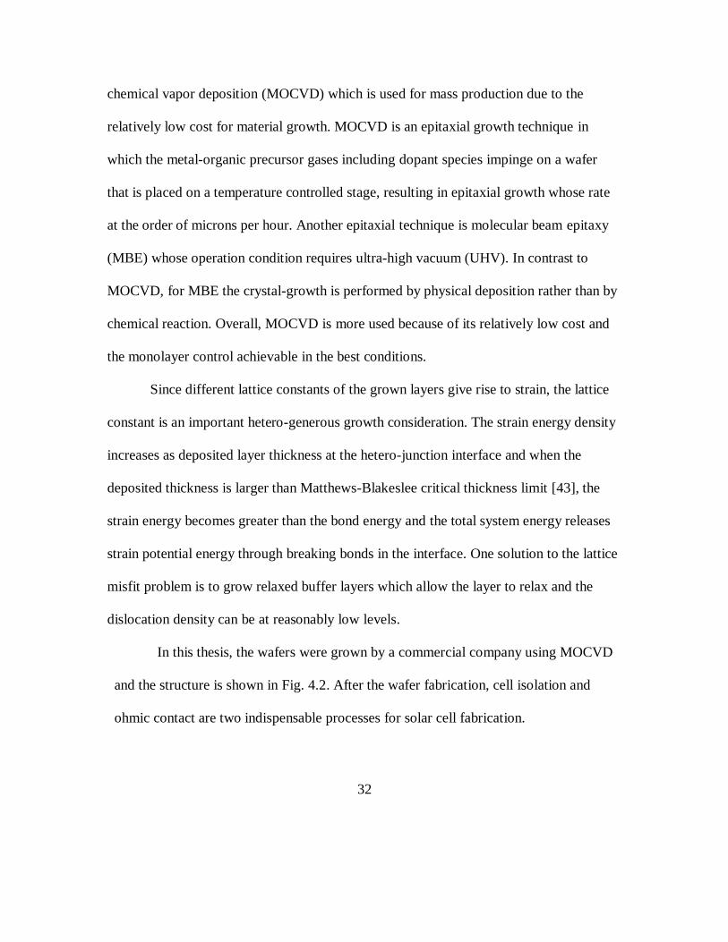
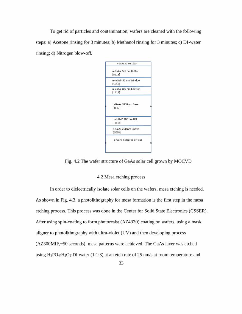
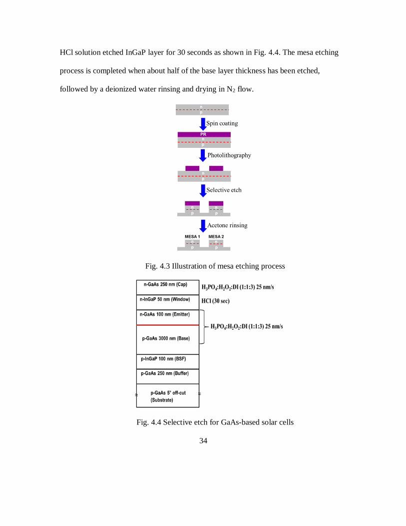
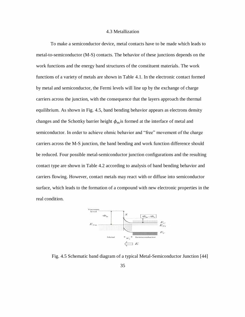
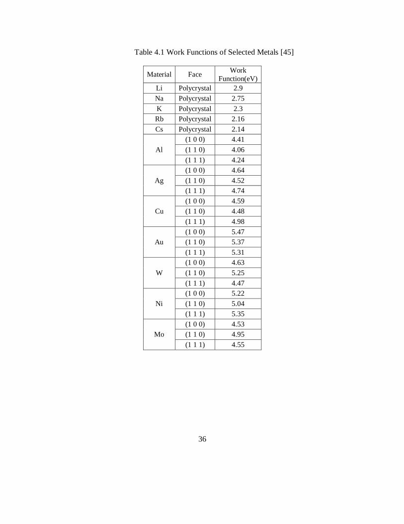
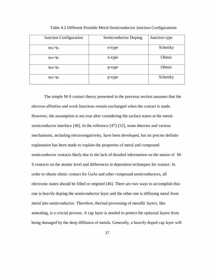
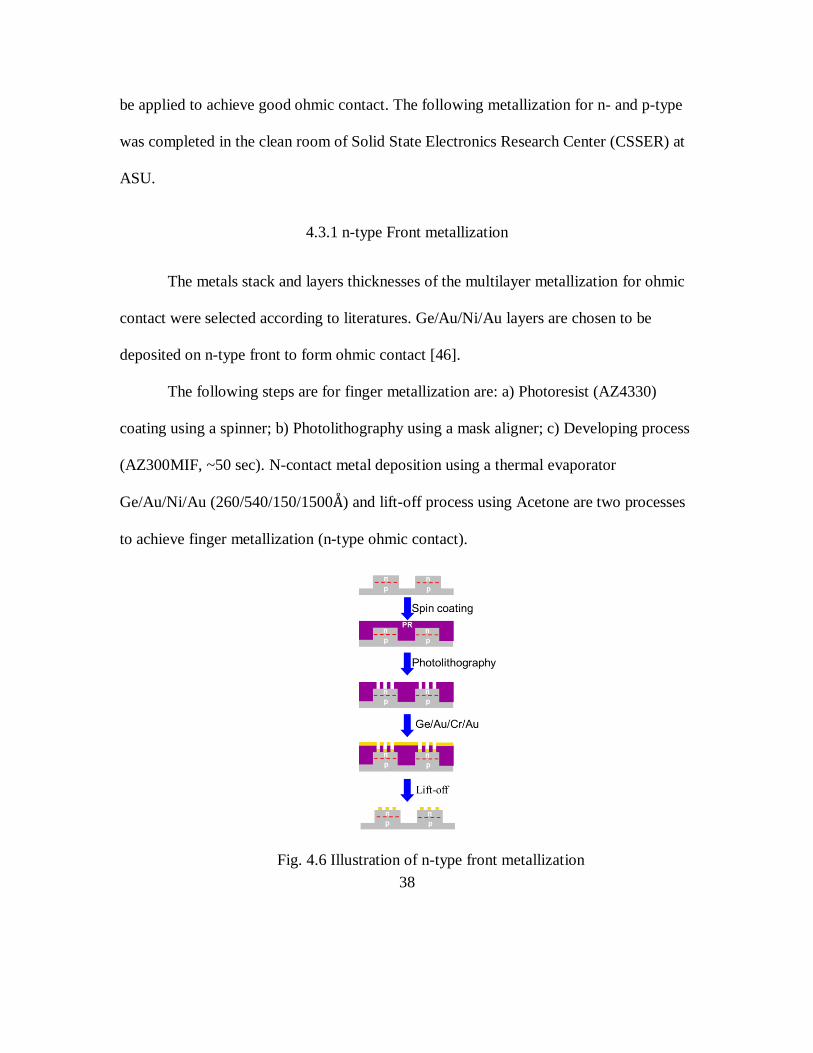
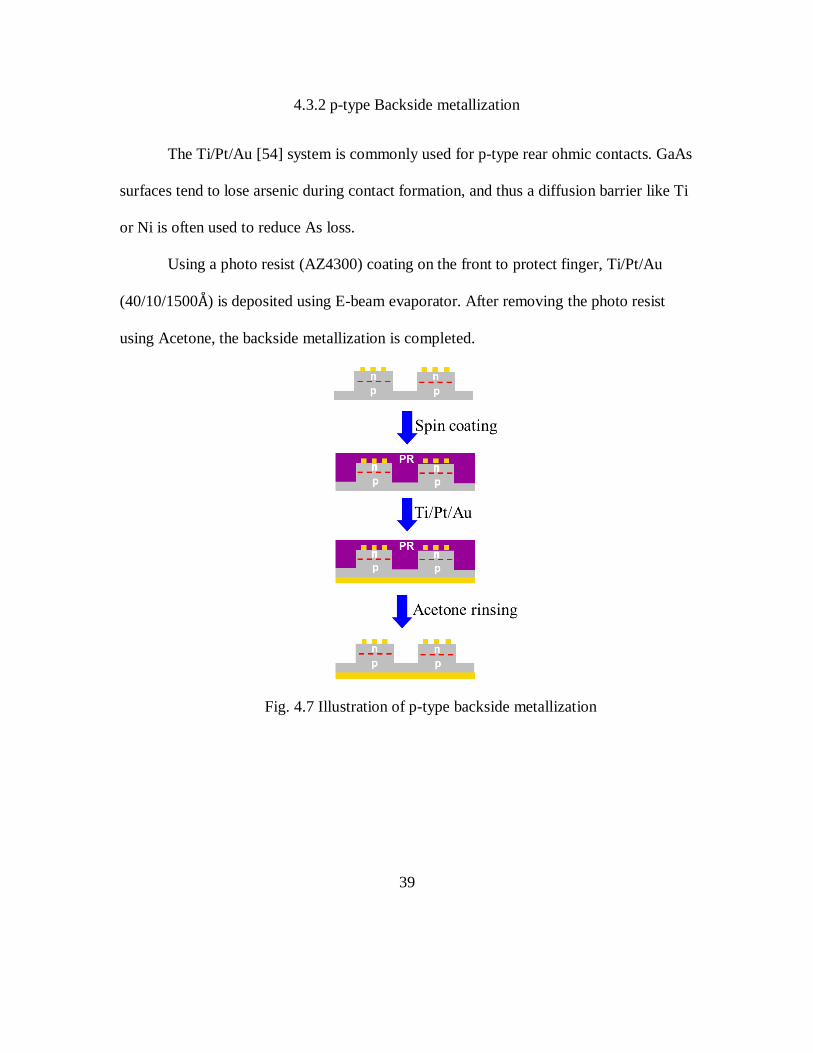
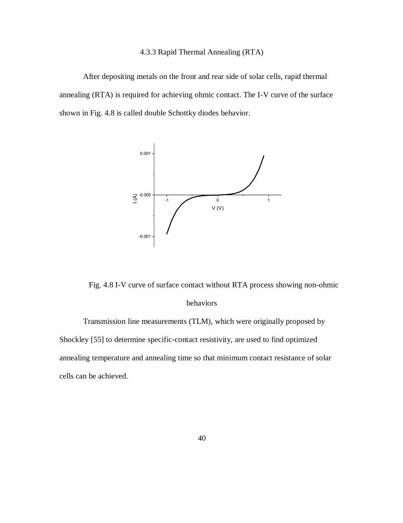
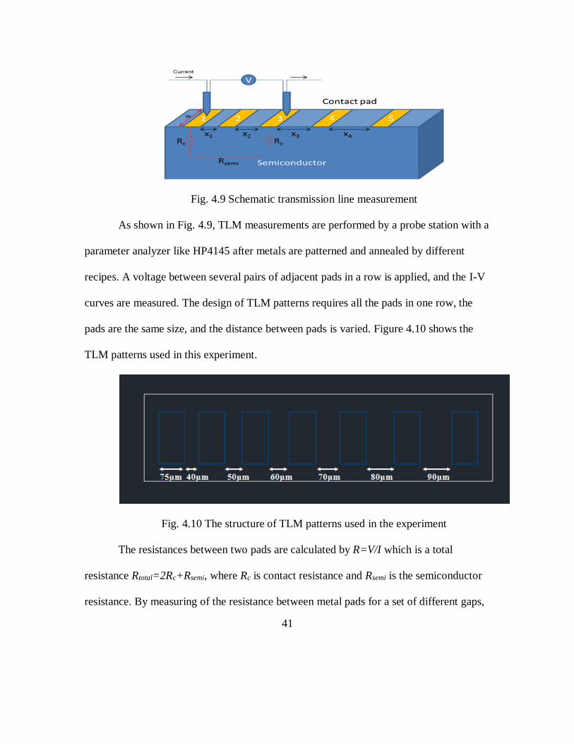
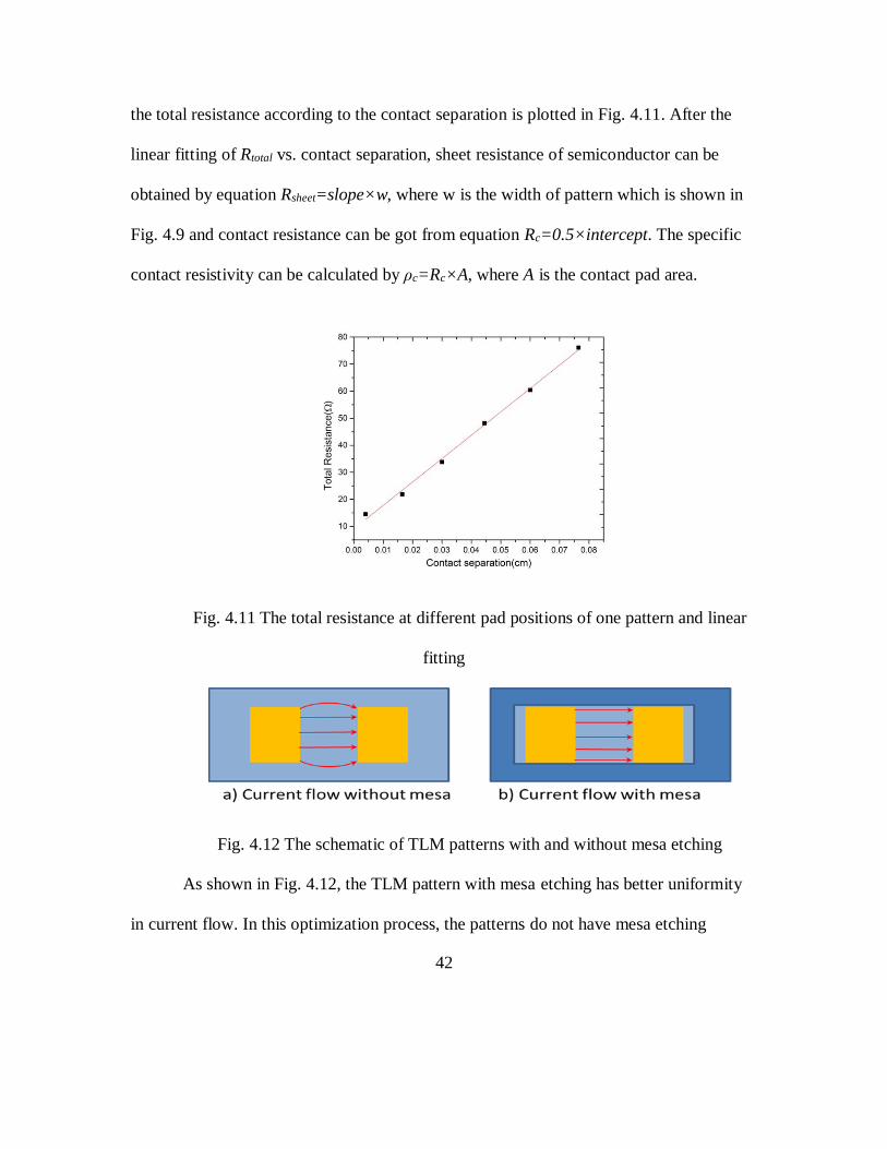
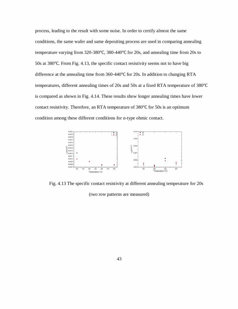
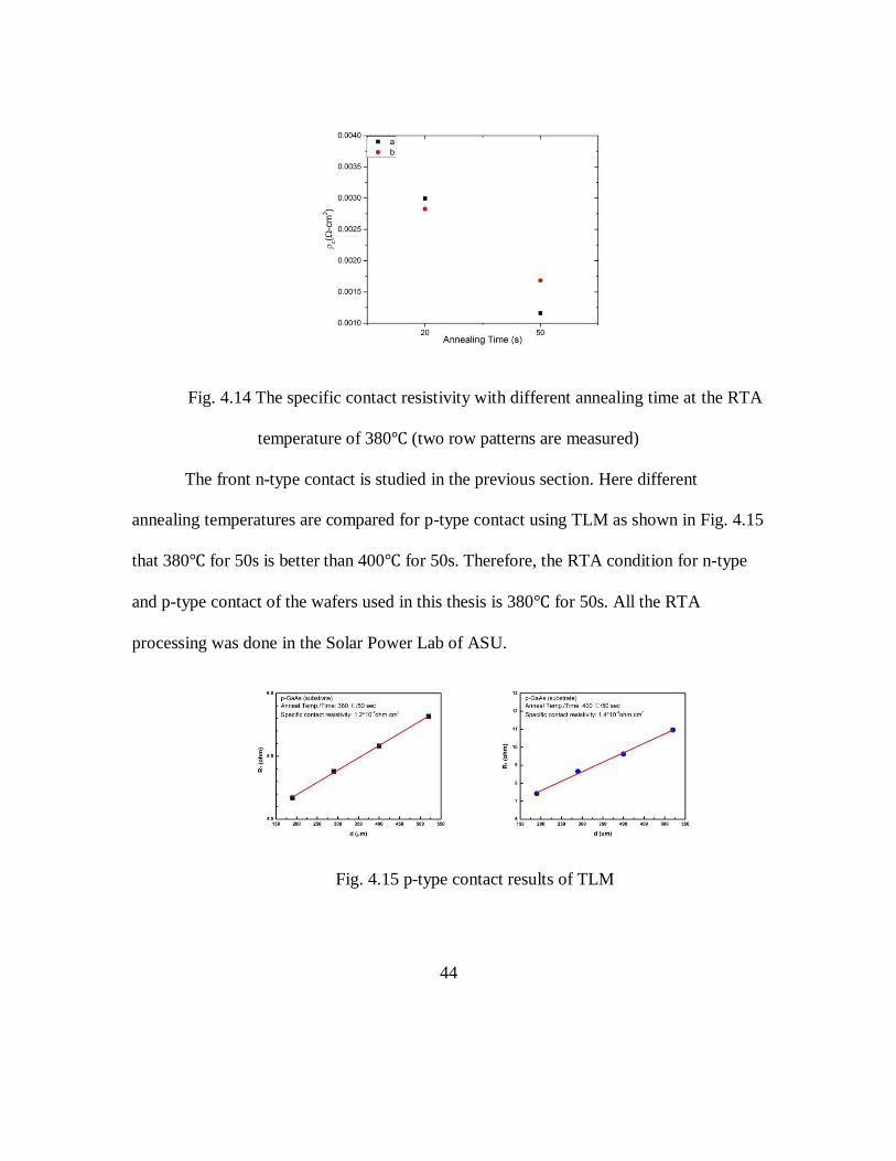
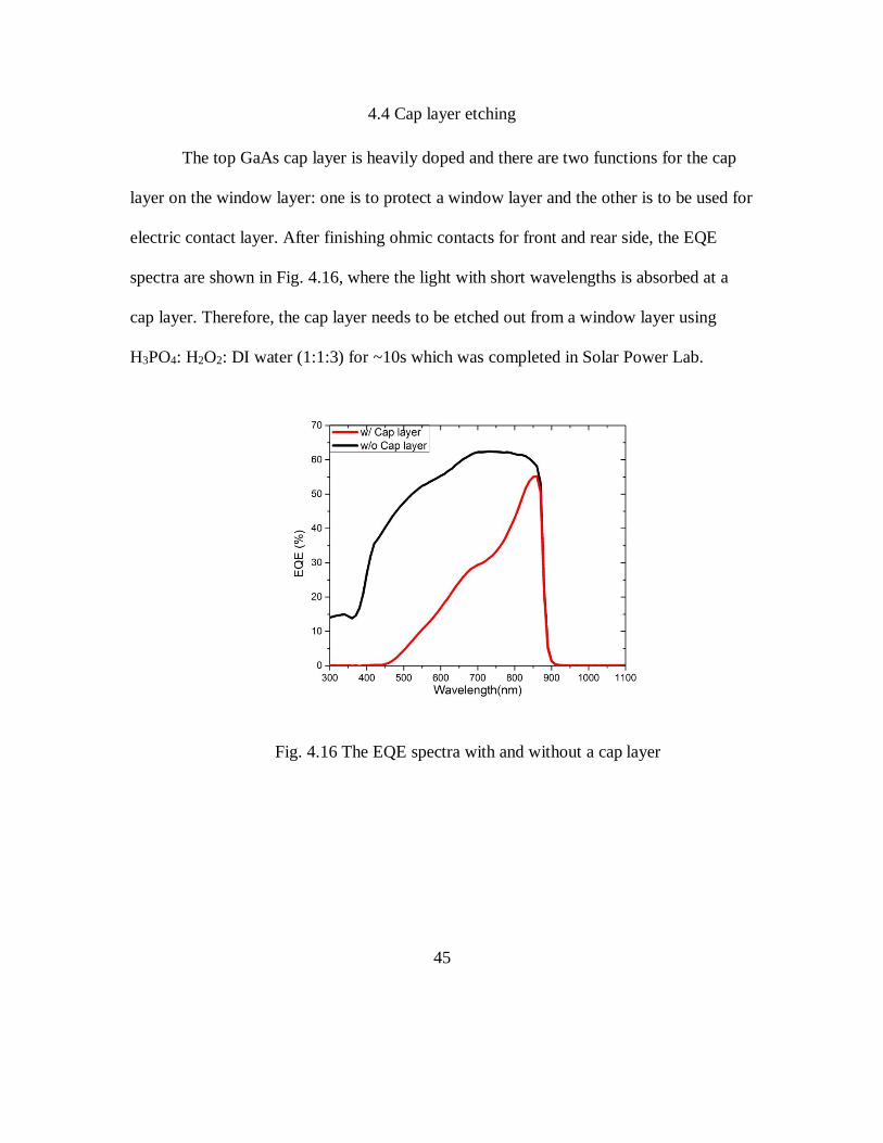
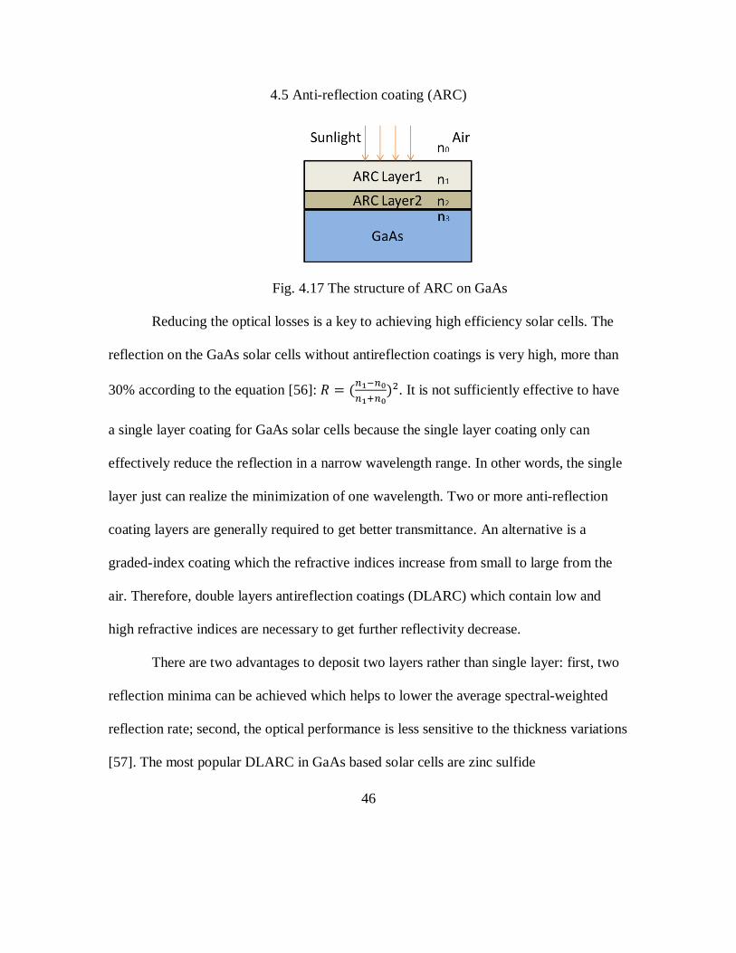
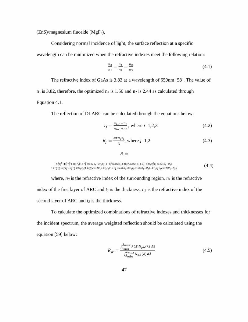
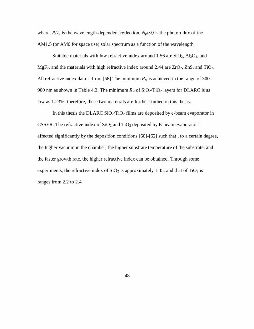
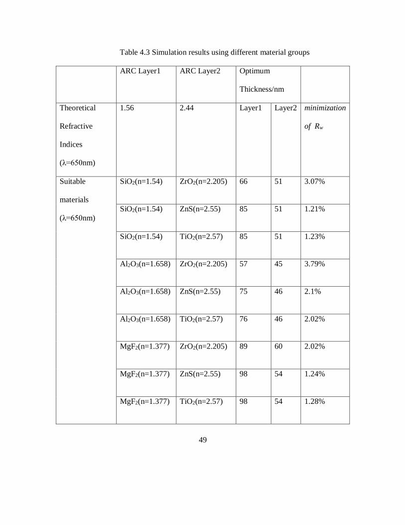
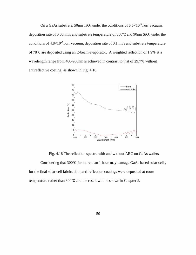
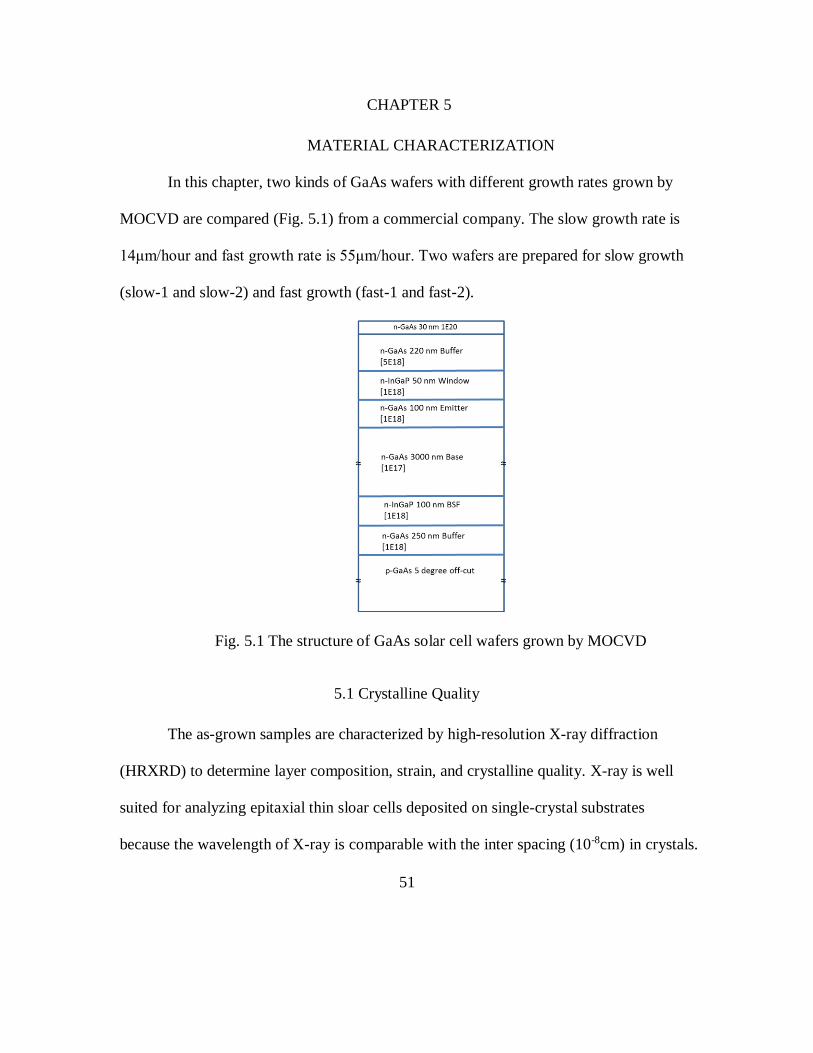
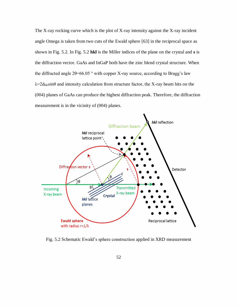
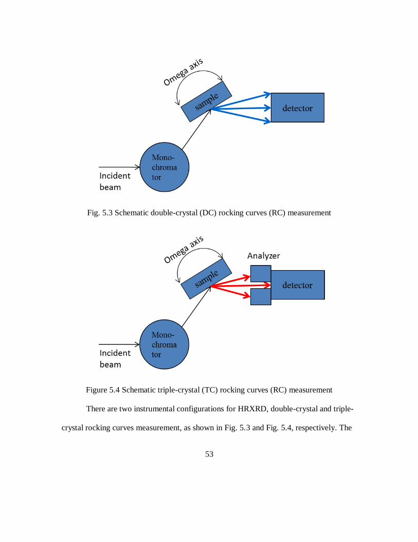
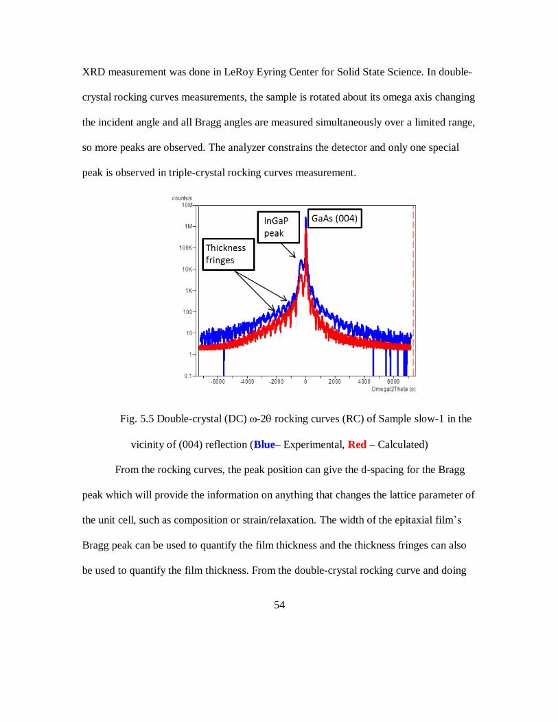
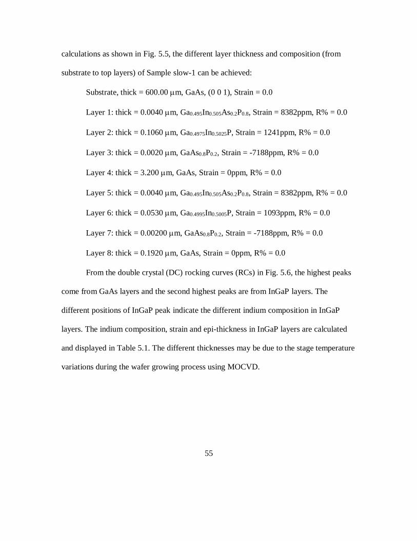
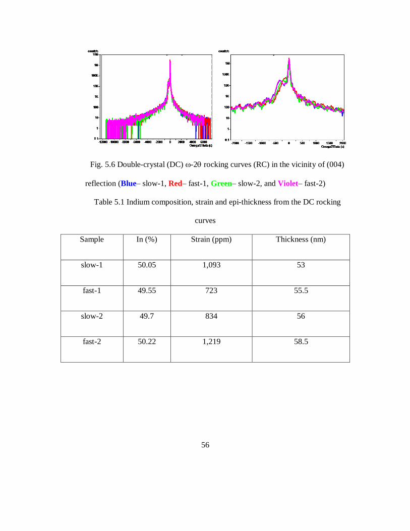
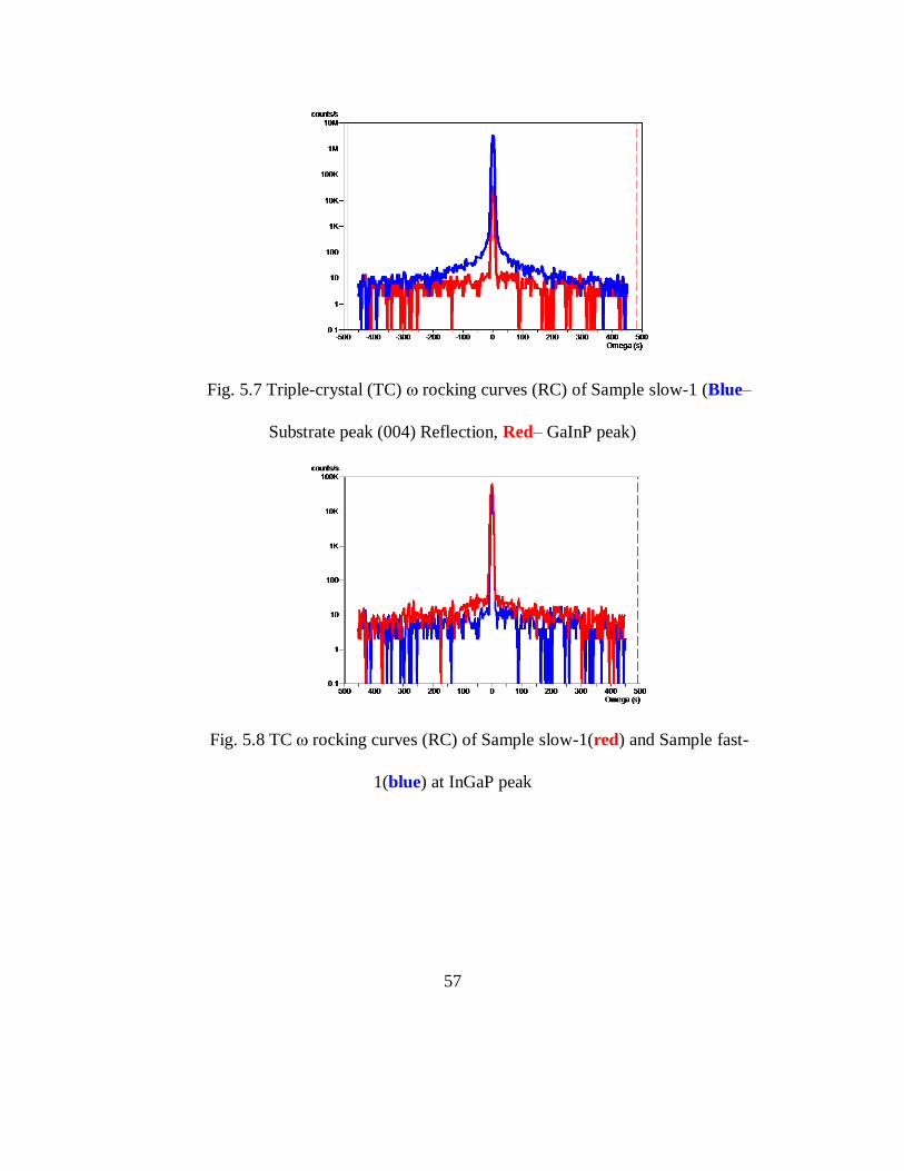
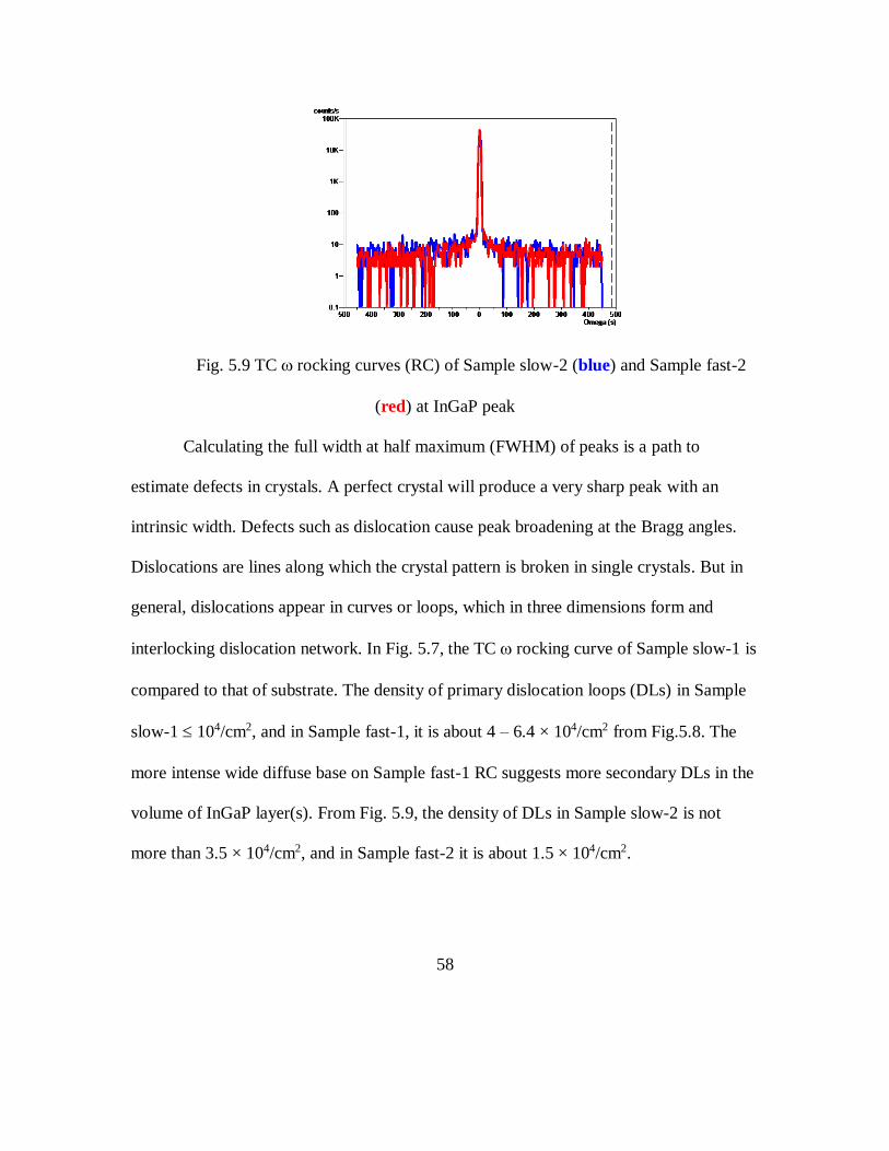
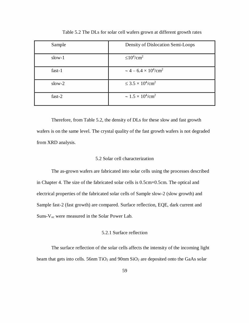
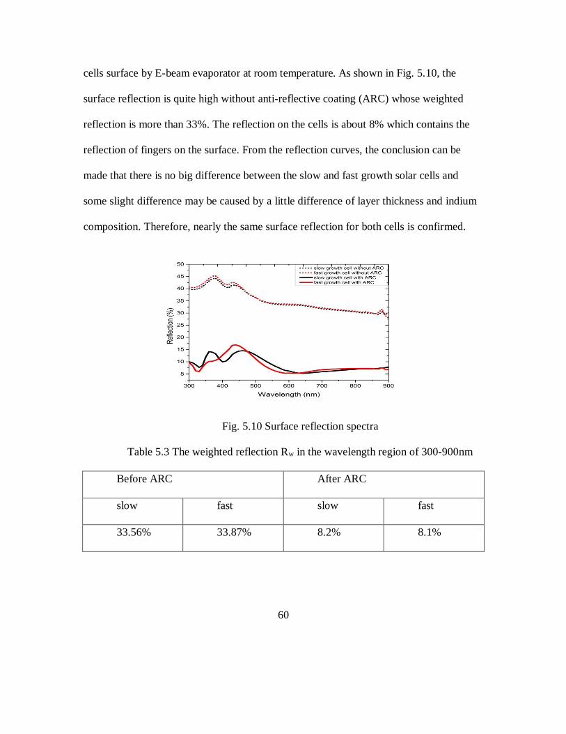
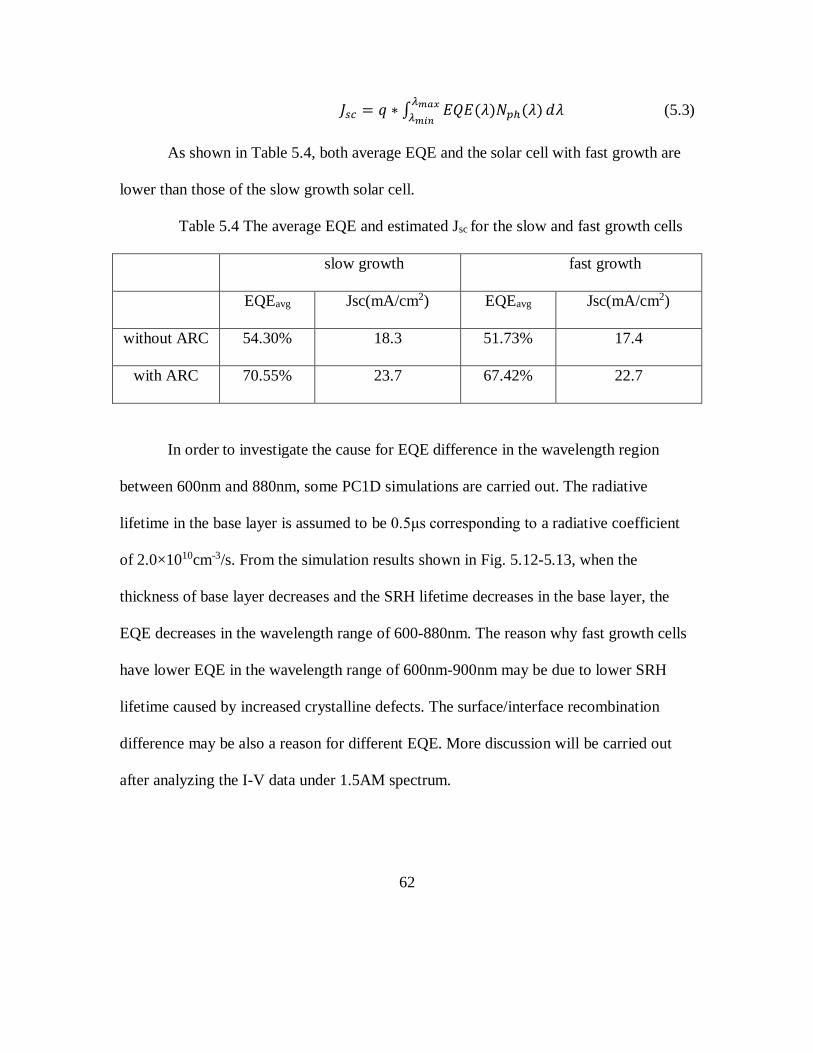
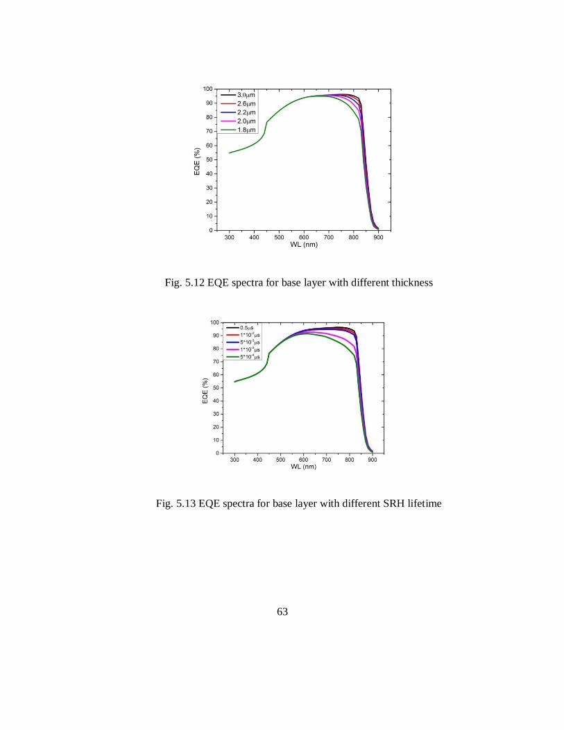
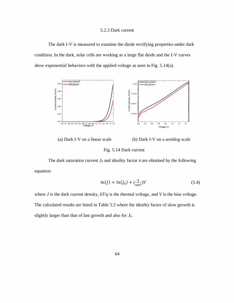
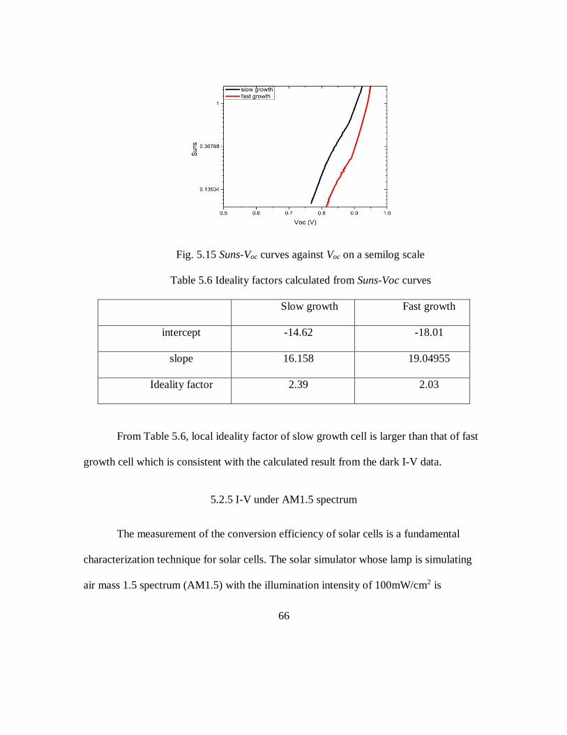
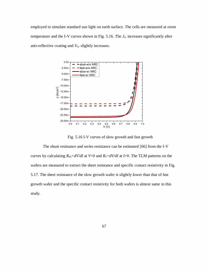
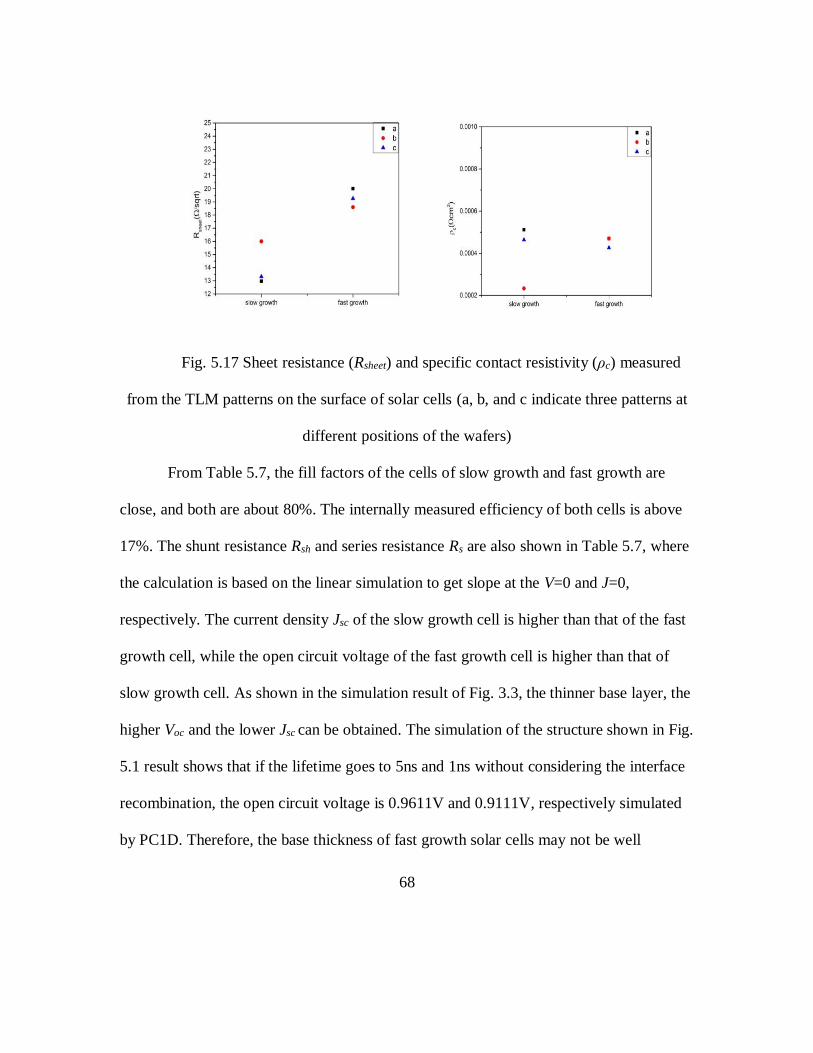
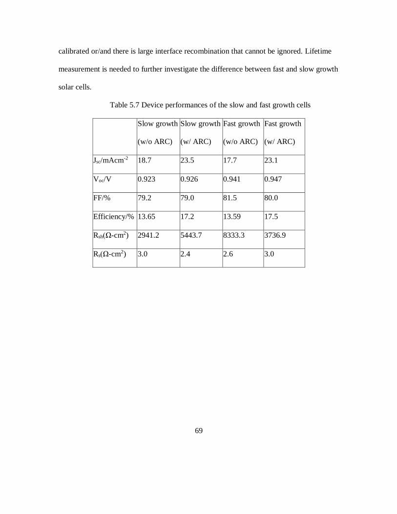


![delano input nr01 sp01.PDF [ 1 ], page 1 @ Normalize ( 01 ... · CIGS panels set a new benchmark for efficiency 13 GaAs solar cells for space hit new milestone 05 Contents FINAL V2.qxp](https://img.pdfslide.us/doc/110x75/6022d99c23814f4b813da3c5/delano-input-nr01-sp01pdf-1-page-1-normalize-01-cigs-panels-set-a.jpg)