Embed Size (px)
Citation preview
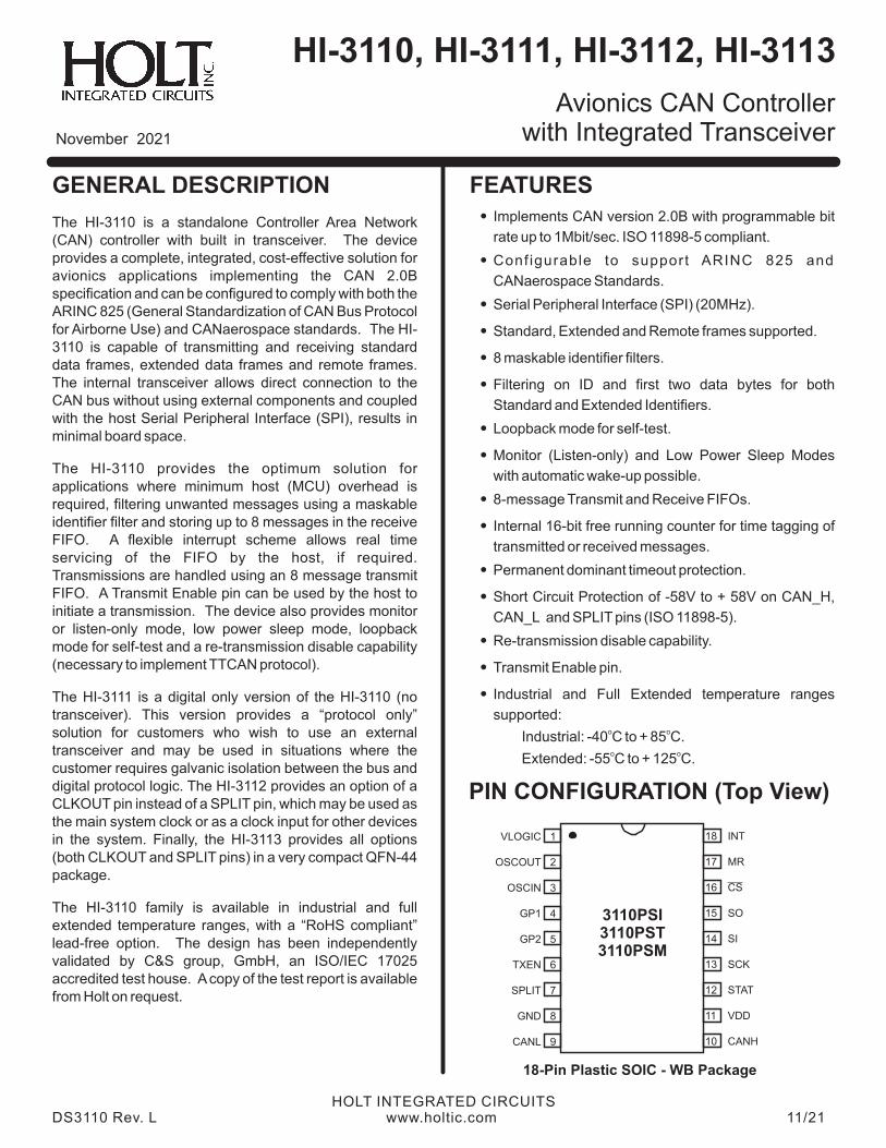
Avionics CAN Controller with Integrated Transceiver
HI-3110, HI-3111, HI-3112, HI-3113
November 2021
GENERAL DESCRIPTION FEATURESImplements CAN version 2.0B with programmable bit The HI-3110 is a standalone Controller Area Network rate up to 1Mbit/sec. ISO 11898-5 compliant. (CAN) controller with built in transceiver. The device
provides a complete, integrated, cost-effective solution for Conf igurable to support ARINC 825 and avionics applications implementing the CAN 2.0B CANaerospace Standards. specification and can be configured to comply with both the ARINC 825 (General Standardization of CAN Bus Protocol for Airborne Use) and CANaerospace standards. The HI- Standard, Extended and Remote frames supported.3110 is capable of transmitting and receiving standard
8 maskable identifier filters. data frames, extended data frames and remote frames. The internal transceiver allows direct connection to the Filtering on ID and first two data bytes for both CAN bus without using external components and coupled Standard and Extended Identifiers. with the host Serial Peripheral Interface (SPI), results in
Loopback mode for self-test. minimal board space.
Monitor (Listen-only) and Low Power Sleep Modes The HI-3110 provides the optimum solution for
with automatic wake-up possible. applications where minimum host (MCU) overhead is
8-message Transmit and Receive FIFOs. required, filtering unwanted messages using a maskable identifier filter and storing up to 8 messages in the receive Internal 16-bit free running counter for time tagging of FIFO. A flexible interrupt scheme allows real time transmitted or received messages. servicing of the FIFO by the host, if required. Transmissions are handled using an 8 message transmit FIFO. A Transmit Enable pin can be used by the host to initiate a transmission. The device also provides monitor or listen-only mode, low power sleep mode, loopback mode for self-test and a re-transmission disable capability (necessary to implement TTCAN protocol).
Extended: -55 C to + 125 C.
The HI-3110 family is available in industrial and full extended temperature ranges, with a “RoHS compliant” lead-free option. The design has been independently validated by C&S group, GmbH, an ISO/IEC 17025 accredited test house. A copy of the test report is available from Holt on request.
·
·
Serial Peripheral Interface (SPI) (20MHz). ·
·
·
·
·
·
·
·
Permanent dominant timeout protection.·
Short Circuit Protection of -58V to + 58V on CAN_H, ·CAN_L and SPLIT pins (ISO 11898-5).
Re-transmission disable capability.·
Transmit Enable pin. ·
Industrial and Full Extended temperature ranges ·The HI-3111 is a digital only version of the HI-3110 (no transceiver). This version provides a “protocol only” supported:
o osolution for customers who wish to use an external Industrial: -40 C to + 85 C. transceiver and may be used in situations where the o o
customer requires galvanic isolation between the bus and digital protocol logic. The HI-3112 provides an option of a CLKOUT pin instead of a SPLIT pin, which may be used as the main system clock or as a clock input for other devices in the system. Finally, the HI-3113 provides all options (both CLKOUT and SPLIT pins) in a very compact QFN-44 package.
PIN CONFIGURATION (Top View)
3110PSI3110PST3110PSM
VLOGIC 1
OSCOUT 2
OSCIN 3
GP1 4
GP2 5
TXEN 6
SPLIT 7
GND 8
CANL 9
18 INT
17 MR
16 CS
15 SO
14 SI
13 SCK
12 STAT
11 VDD
10 CANH
18-Pin Plastic SOIC - WB Package
HOLT INTEGRATED CIRCUITSDS3110 Rev. L www.holtic.com 11/21
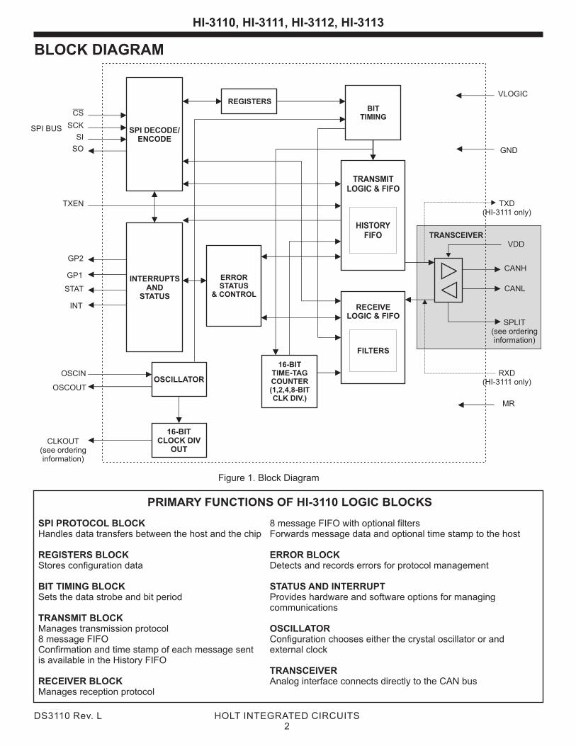
BLOCK DIAGRAM
16-BITTIME-TAG COUNTER(1,2,4,8-BITCLK DIV.)
SPI PROTOCOL BLOCKHandles data transfers between the host and the chip
REGISTERS BLOCKStores configuration data
Sets the data strobe and bit period
TRANSMIT BLOCKManages transmission protocol 8 message FIFO Confirmation and time stamp of each message sent is available in the History FIFO
8 message FIFO with optional filters Forwards message data and optional time stamp to the host
ERROR BLOCKDetects and records errors for protocol management
BIT TIMING BLOCK STATUS AND INTERRUPTProvides hardware and software options for managing communications
OSCILLATORConfiguration chooses either the crystal oscillator or and external clock
TRANSCEIVERRECEIVER BLOCK Analog interface connects directly to the CAN busManages reception protocol
PRIMARY FUNCTIONS OF HI-3110 LOGIC BLOCKS
Figure 1. Block Diagram
HI-3110, HI-3111, HI-3112, HI-3113
OSCOUT
OSCIN
GP1
GP2
SCK
SI
SO
SPI BUS
CS
INT
VDD
GND
MR
TRANSCEIVER
CANL
CANH
STAT
TXEN
VLOGIC
OSCILLATOR
INTERRUPTSAND
STATUS
ERRORSTATUS
& CONTROL
REGISTERS
TRANSMITLOGIC & FIFO
HISTORYFIFO
RECEIVELOGIC & FIFO
FILTERS
SPI DECODE/ENCODE
BITTIMING
CLKOUT(see orderinginformation)
16-BITCLOCK DIV
OUT
SPLIT(see orderinginformation)
TXD(HI-3111 only)
RXD(HI-3111 only)
DS3110 Rev. L2
HOLT INTEGRATED CIRCUITS
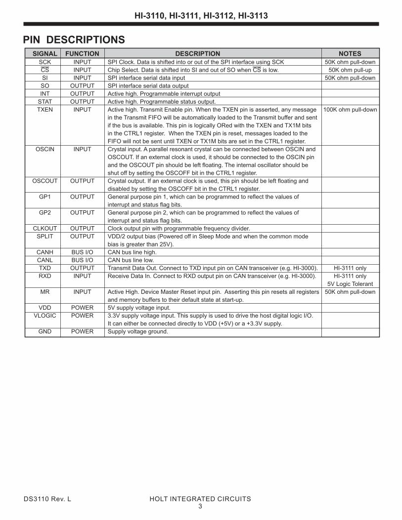
SIGNAL FUNCTION DESCRIPTION NOTESSCK INPUT SPI Clock. Data is shifted into or out of the SPI interface using SCK 50K ohm pull-down
CS INPUT Chip Select. Data is shifted into SI and out of SO when CS is low. 50K ohm pull-up
SI INPUT SPI interface serial data input 50K ohm pull-down
SO OUTPUT SPI interface serial data output
INT OUTPUT Active high. Programmable interrupt output
STAT OUTPUT Active high. Programmable status output.
TXEN INPUT Active high. Transmit Enable pin. When the TXEN pin is asserted, any message 100K ohm pull-down
in the Transmit FIFO will be automatically loaded to the Transmit buffer and sent
if the bus is available. This pin is logically ORed with the TXEN and TX1M bits
in the CTRL1 register. When the TXEN pin is reset, messages loaded to the
FIFO will not be sent until TXEN or TX1M bits are set in the CTRL1 register.
OSCIN INPUT Crystal input. A parallel resonant crystal can be connected between OSCIN and
OSCOUT. If an external clock is used, it should be connected to the OSCIN pin
and the OSCOUT pin should be left floating. The internal oscillator should be
shut off by setting the OSCOFF bit in the CTRL1 register.
OSCOUT OUTPUT Crystal output. If an external clock is used, this pin should be left floating and
disabled by setting the OSCOFF bit in the CTRL1 register.
GP1 OUTPUT General purpose pin 1, which can be programmed to reflect the values of
interrupt and status flag bits.
GP2 OUTPUT General purpose pin 2, which can be programmed to reflect the values of
interrupt and status flag bits.
CLKOUT OUTPUT Clock output pin with programmable frequency divider.
SPLIT OUTPUT VDD/2 output bias (Powered off in Sleep Mode and when the common mode
bias is greater than 25V).
CANH BUS I/O CAN bus line high.
CANL BUS I/O CAN bus line low.
TXD OUTPUT Transmit Data Out. Connect to TXD input pin on CAN transceiver (e.g. HI-3000). HI-3111 only
RXD INPUT Receive Data In. Connect to RXD output pin on CAN transceiver (e.g. HI-3000). HI-3111 only
5V Logic Tolerant
MR INPUT Active High. Device Master Reset input pin. Asserting this pin resets all registers 50K ohm pull-down
and memory buffers to their default state at start-up.
VDD POWER 5V supply voltage input.
VLOGIC POWER 3.3V supply voltage input. This supply is used to drive the host digital logic I/O.
It can either be connected directly to VDD (+5V) or a +3.3V supply.
GND POWER Supply voltage ground.
PIN DESCRIPTIONS
HI-3110, HI-3111, HI-3112, HI-3113
DS3110 Rev. L3
HOLT INTEGRATED CIRCUITS
RECEIVERFUNCTIONAL OVERVIEWThe receiver state machine automatically handles all CAN
The HI-3110 is the first single chip product to integrate both 2.0B protocol requirements. The receiver supports eight the CAN (Controller Area Network) protocol and analog sets of filters and masks and each allows filtering of a full interface transceiver on a single IC. The protocol conforms
CAN ID (extended or not) and two bytes of data. Even when to CAN version 2.0B and is compliant with ISO 11898-
filtering is enabled, message data is always accessible as 1:2003(E) specification. The transceiver is compliant with received via the Temporary Receive Buffer, and retrievable ISO 11898-5 specification.by SPI op codes 0x42 and 0x44.
If the Filter/Mask option is set (FILTON bit in Control Register Configuration options include an internal Loopback mode
1), only messages that match one of the 8 stored data that does not disturb the bus, a Monitor only mode, and a
patterns are passed into the FIFO. Note that the Mask option Sleep mode that includes an option to either wake up
allows certain bits of the programmed filter bits to be “don't automatically when data is present on the bus, or by host
care.” If the Filter/Mask option is not set, then all valid command. The following sections describe some of the key
messages are passed to the FIFO. When the FIFO is full (8 features.
completed messages received), the next received message SPI and REGISTERS will overwrite the latest message stored in the FIFO.To minimize the footprint, a 20 MHz standard four wire SPI
(Serial Peripheral Interface) is provided to manage the flow ERROR CONTROLof data between the host microcontroller and the HI-3110. Errors are detected per ISO 11898-1:2003(E) and Complete messages are loaded and retrieved with single detections are counted and used by the protocol state SPI op codes. On the receive side, SPI op code options may machines. Active, Passive, and Bus Off conditions are be used to retrieve the whole message or just the data. An managed per the CAN standard. A configuration bit is option to include a time tag or no time tag may also be provided to allow automatic recovery from Bus Off.specified. On the transmit side, each message can be
assigned an identifier which allows monitoring of the STATUS and INTERRUPTSTransmit History FIFO to confirm the successful completion The Message Status Register, MESSTAT, provides of a transmission along with the time stamp. In addition the information about the current state of the receiver and transmitter logic automatically assembles the message transmitter operation. In addition, the Interrupt Flag frame based on the data presented. Register, INTF, monitors 8 operational conditions, any or all
of which may be directed to the INT pin by enabling bits in the BIT TIMING Interrupt Enable Register, INTE. Similarly, the Status Flag Bit timing is controlled with standard CAN options. These Register, STATF, bits reflect the status of selected FIFO and include control of the Resychronization Jump Width (SJW), Error properties. Any or all of these conditions may be Prop delay Phase Seg 1 (TSeg1), Phase Seg 2 (TSeg2), the directed to the STAT pin by setting the enable bits in the number of samples, and the derivation of Tq from the system Status Flag Enable Register, STATFE. clock using a prescaler. The maximum bit rate is 1 MBit/sec. To provide additional hardwired flag options, the GP1 and Upon reset, the chip automatically enters Initialization mode GP2 pins may also be programmed to reflect any of the which allows programming of the Bit Timing before entering Interrupt or Status Flag bits.Normal mode.
OSCILLATOR and TIME TAGTRANSMITTER A configuration bit allows a choice for the source of the The transmitter state machine automatically handles all system clock. Either the on-board crystal oscillator may be CAN 2.0B protocol requirements. Messages for selected or an external clock may be provided at the OSCIN transmission are first loaded into a FIFO and transmission pin.may start upon availability of data in the FIFO. Assertion of On product versions with the CLKOUT pin, a programmable the TXEN pin or configuration bits in Control Register 1 allow division of the system clock is provided. The clock source for either continuous transmission until the FIFO is empty or the 16 bit Time Tag Counter is derived from a separate only one message from the FIFO at a time. One shot (no programmable division of the system clock. SPI op codes retry) transmission may also be enabled by setting the OSM provide for reading and resetting the Time Tag Counter. and TX1M bits. SPI op codes are provided to clear the TRANSCEIVER Transmit FIFO and to abort transmission. The HI-3110 contains an integrated transceiver operating
HI-3110, HI-3111, HI-3112, HI-3113
DS3110 Rev. L4
HOLT INTEGRATED CIRCUITS
from 5V and the line driver is capable of maintaining a MONITOR MODE
detectable signal for bus lengths well in excess of
recommended CAN 2.0B standards. The digital logic and IO Monitor mode (also known as listen-only or silent mode) can be powered from 3.3V or 5V. allows the HI-3110 to monitor all bus activity without
disturbing the bus. No messages or dominant bits (such as ACK or active error frame bits) are transmitted to the bus PROTECTION FEATURESwhile in this mode. Also, the error counters are reset and The BUS and SPLIT pins are protected against ESD to over deactivated. Messages from the bus are received in the 4KV (HBM) and from shorts between -58V to +58V same way as Normal Mode and messages that are not
continuous, as specified in ISO 11898-5. acknowledged by another node on the bus are ignored i.e.
In addition, a Permanent Dominant Timeout protection is any frame containing an error will be ignored. Acceptance
implemented by means of an independent counter filters can be set up to reject or accept specific messages monitoring the dominant transmission state and into the FIFO and all interrupt flags are set as required in the automatically shutting off the transmission if it exceeds usual way. Monitor mode is activated by programming the
MODE<2:0> bits to <010> in the CTRL0 register. typically 2ms.
SLEEP MODE
MODES OF OPERATION The HI-3110 can be placed in a low power sleep mode if there is no bus activity and the transmit FIFO is empty. In
The HI-3110 supports five modes of operation, namely, this mode, the internal oscillator and all analog circuitry
Initialization Mode, Normal Mode, Loopback Mode, Monitor (transceiver) are off, drawing typically less than 20mA. Note
Mode and Sleep Mode. that the SPI bus is active during sleep mode, so it is possible for the host to communicate with the HI-3110 while it is INITIALIZATION MODEasleep (e.g. load transmit FIFO). Sleep mode is exited by selecting an alternative mode of operation, or automatic Initialization mode is used to configure the device before wake up following bus activity can be enabled by setting the normal operation. Bit timing registers and acceptance WAKEUP bit in the CTRL0 register - in this case a low power filters and masks can only be modified in this mode. receiver monitors the bus for a detectable dominant bit.. Initialization mode is the default mode following RESET and The device will wake up in Monitor Mode. Note that it will can also be activated by programming the MODE<2:0> bits take a finite time for the oscillator and analog circuitry to to <1xx> in the CTRL0 register. Switching to Initialization come back on line. Since the internal oscillator takes a finite mode resets the receiver and transmitter. During time to wake up, the message which caused the wake-up initialization mode, the error counters are held reset. may not be stored.
NORMAL MODESleep mode is activated by programming the MODE<2:0> bits to <011> in the CTRL0 register. However, the actual Normal mode is the standard operating mode of the HI-3110. mode change will only occur whenever the CAN bus is quiet. In this mode, the HI-3110 can transmit, receive and If the chip is transmitting, the mode change is delayed until acknowledge messages from the CAN bus, handling all the transmission is complete. If there is bus activity, the aspects of the CAN protocol. Normal mode is activated by mode change is delayed until the receiver protocol control programming the MODE<2:0> bits to <000> in the CTRL0 detects an inter-message gap.register.
LOOPBACK MODE CAN PROTOCOL OVERVIEW
Loopback mode is used for self-test. The transceiver digital The HI-3110 supports Standard, Extended and Remote input is fed back to the receiver without being transmitted to Frames, as defined in the CAN specification IS0 11898-the bus. Messages are transmitted from the transmit FIFO 1:2003(E) (also known as CAN 2.0B). in the usual way and received by the receive FIFO as if they were received from a remote node on the bus. BIT ENCODING
Acceptance filters can be set up to accept or reject specific CAN frames are encoded according to the Non-Return-To-messages into the FIFO and all interrupt flags are set as Zero (NRZ) method with bit stuffing. NRZ means that the required in the usual way. While in this mode, any bus generated bit level is constant during the total bit time and activity is ignored. Loopback is activated by programming consecutive bits do not return to a neutral or rest condition. the MODE<2:0> bits to <001> in the CTRL0 register.
HI-3110, HI-3111, HI-3112, HI-3113
DS3110 Rev. L5
HOLT INTEGRATED CIRCUITS
This means that a bit stream of “1s” or “0”s appears errors by computing a 15-bit CRC sequence from the continuous on the bus. A logic “0” is called a dominant bit previous bit stream (SOF, arbitration field, control field and and a logic “1” is called a recessive bit. data field, excluding stuff bits). The last bit in the CRC field is
the CRC delimiter bit (always recessive). Bit stuffing is used to ensure frequent enough transitions occur to achieve synchronization. Every time a transmitter After the CRC field is the Acknowledge Field (ACK Field). detects five consecutive bits of the same polarity in the bit The first bit is the ACK Slot bit. A transmitting node sends a stream to be transmitted, it inserts a bit of opposite polarity recessive bit (logic 1) during the ACK slot. Any node which into the actual transmitted bit stream. receives the message error-free acknowledges the
reception by placing a dominant bit (logic 0) in the ACK slot, This bit stuffing rule applies to the Start-of-Frame field, over-writing the recessive bit of the transmitter. The final bit arbitration field, control field, data field and CRC sequence. in the ACK field is a recessive ACK delimiter bit. Therefore, The CRC delimiter, ACK field and End-Of-Frame fields are of the dominant ACK slot bit is surrounded on each side by a fixed form and not stuffed (see below for definition of these recessive bit. fields). Furthermore, Error frames and Overload frames are also of fixed form and not stuffed. Each data frame is delimited by an End-Of-Frame field
(EOF). The EOF consists of seven recessive bits. An example of how the bits in a stuffed bit stream might look is shown below. Following the EOF, there is a gap to the next frame called the
Interframe Space (IFS) . The IFS consists of two bit fields, 00101011111O0000I1100000I11000 Intermission and Bus-Idle. The Intermission consists of
three recessive bits, however the following notes apply: 0 = dominant bit, O = dominant stuffed bit. a) detection of a dominant bit on the bus at the third slot is 1 = recessive bit, I = recessive stuffed bit. interpreted as a SOF,
b) detection of a dominant bit in either the first or second MESSAGE FRAMES slots results in generation of an overload frame (see below).
STANDARD DATA FRAME The bus idle period is of arbitrary length and consists of The standard data frame is shown in figure 2. The frame recessive bits. A dominant bit detected during this period is starts with a Start-of-Frame (SOF) bit. This is a dominant bit interpreted as a SOF. that identifies the start of the data frame on the bus.
EXTENDED DATA FRAMEThe SOF is followed by the 12-bit arbitration field. The The extended data frame is shown in figure 3. In this frame arbitration field consists of an 11-bit identifer, ID28 - ID18, format, SOF is followed by a 32-bit arbitration field consisting and the Remote Transmission Request (RTR) bit. The RTR of a 29-bit identifier, ID28 - ID0. The first 11 most significant bit is used to distinguish between a data frame (RTR bit bits of the ID are know as the base identifier. This is followed dominant, logic 0) and a remote frame (RTR bit recessive, by the Substitute Remote Request (SRR) bit, which is logic 1). defined as recessive. Following the SRR bit is the IDE bit,
which is defined as recessive for extended data frames. Following the arbitration field is the 6-bit control field. The
Note that the SRR bit is in the same slot as the RTR bit of the first bit of the control field is the Identifier Extension flag bit
standard frame and the IDE bits are also in corresponding (IDE). This is used to distinguish between standard and
slots. This means if standard and extended identifier data extended identifiers and must be dominant (logic 0) for
frames with identical base identifiers are transmitted standard data frames. The next bit, r0, is specified by the
simultaneously, the standard identifier data frame will win CAN protocol as a reserved bit for future expansion. This bit
arbitration (see Bitwise Arbitration section below). must be transmitted dominant, but receivers must be capable of receiving either a dominant or recessive bit. The The SRR and IDE bits are followed by the remaining 18 bits final 4 bits of the control field make up the data length code of the identifier (extended ID) and the last bit of the (DLC). The binary value of this 4-bit field specifies the arbitration field is the RTR bit. The RTR bit has the same number of data bytes in the data payload (0 - 8 bytes). Note: function as in the standard frame format. All binary combinations greater than or equal to <1 0 0 0> specify 8 bytes of data. Following the arbitration field is the 6-bit control field. The
first two bits, r1 and r0, are specified by the CAN protocol as After the control field is the data field, which contains a data reserved bits for future expansion. Both these bits must be payload equal to the number of bytes specified by the DLC transmitted dominant, but receivers must be able to receive (see note above). all combinations of dominant or recessive bits. The final 4
bits of the control field is the data length code (DLC). The The data field is followed by the 16-bit Cyclic Redundancy
binary value of this 4-bit field specifies the number of data Check (CRC) field. This is used to check transmission
bytes in the data payload (0 - 8 bytes). Note: All binary
HI-3110, HI-3111, HI-3112, HI-3113
DS3110 Rev. L6
HOLT INTEGRATED CIRCUITS

combinations greater than or equal to <1 0 0 0> specify 8 it must wait for 6 consecutive bits of equal polarity before bytes of data. completing the error flag. If the passive error flag is generated by a transmitter, the bit stuffing rule is violated and
it will cause other nodes to generate error flags. Two The remaining fields of the extended data frame (Data field, exceptions to this rule are CRC field, acknowledge field, EOF field and IFS field) are a) the passive error flag starts during arbitration and another constructed in the same way as the standard frame format. node prevails and begins transmitting, and
b) the error flag starts less than 6 bits before the end of the REMOTE FRAME CRC sequence and the last bits of the CRC sequence all The remote frame is shown in figure 4. The function of happen to be recessive. remote frames is to allow a receiver which periodically receives certain types of data to request that data from the OVERLOAD FRAMEtransmitting source. The identifier of the remote frame must The overload frame is shown in figure 6. It has the same be identical to the identifier of the requested transmitting format as the active error frame, consisting of an overload node’s data frame and the data length code (DLC) should be flag field and an overload delimiter. The overload flag equal to the DLC of the requested data. Simultaneous consists of 6 consecutive dominant bits. This condition transmission of remote frames with the same identifier violates the rule of bit-stuffing and causes all other nodes on and different DLCs will lead to unresolvable collisions the bus to generate echo flags, similar to the active error flag on the bus. For this reason, ARINC 825 strongly echos. Therefore, the overload flag field will consist of the discourages the use of remote frames. superposition of different overload flags sent by individual
nodes, resulting in a minimum of 6 and maximum of 12 The format of a remote frame is identical to the format of the consecutive dominant bits. The overload flag is followed by corresponding data frame except the remote frame has no the overload delimiter, consisting of 8 recessive bits. data payload. Remote frames and data frames are distinguished by a recessive RTR bit in the remote frame. An overload frame, unlike an error frame, can only be This means if a receiver sends a remote frame and the generated during the interframe space. There are two types sending node transmits at the same time, the sending node of overload frame:(with a dominant RTR bit) will win arbitration and the
1) Reactive Overload Frame, resulting from requesting node will receive the desired data immediately. a) detection of a dominant bit during the first or second bit of
ERROR FRAME intermission, The error frame is shown in figure 5. Any node detecting an b) detection of a dominant bit at the last (seventh) bit of EOF error generates an error frame. The error frame consists of in received frames, or
c) detection of a dominant bit at the last (eighth) bit of an error two fields, the error flag field and the error delimiter. The delimiter or overload delimiter. type of error flag field depends on the error status of the The reactive overload frame is started one bit after detecting node, error-active or error-passive (see below). An error-any of the above dominant bit conditions. active node generates an active error flag and an error-
passive node generates a passive error flag. 2) Requested Overload Frame. A node which is unable to begin reception of the next message due to internal Active Error Flag: An active error flag consists of 6 conditions may request a delay by transmitting a maximum consecutive dominant bits. This condition violates the rule of two consecutive overload frames. The requested of bit-stuffing and causes all other nodes on the bus to overload frame must be started at the first bit of an expected generate error flags, known as echo error flags. Therefore, intermission. the error flag field will consist of the superposition of different
error flags sent by individual nodes, resulting in a minimum Note 1): The HI-3110 will never initiate an overload frame of 6 and maximum of 12 consecutive dominant bits. The unless reacting to one of the conditions in case 1) above. error flag field is followed by the error delimiter, consisting of Note 2): Initiation of overload frames is prohibited by ARINC
8 recessive bits. 825 since they increase the network loading.
Passive Error Flag: A passive error flag consists of 6 recessive bits. This is followed by the 8 recessive bits of the error delimiter. Therefore, an error frame sent by an error-passive node consists of 14 consecutive recessive bits. Since this will not disturb the bus, a transmitting node will continue to transmit unless it detects the error itself, or another error-active node detects the error.
Notes: If the passive error flag is generated by a receiver, it cannot prevail over any other activity on the bus. Therefore,
HI-3110, HI-3111, HI-3112, HI-3113
DS3110 Rev. L7
HOLT INTEGRATED CIRCUITS
Standard Data Frame
KEY.
SOF Start-Of-FrameIDxx Identifier bit xxRTR Remote Transmission Request bitIDE Identifier Extension Flagr0 Reserved bit 0DLCx Data Length Code bit xCRC Del Cyclic Redundancy Check DelimiterACK Slot bit Acknowledge Slot bitACK Del Acknowledge DelimiterEOF End-Of-FrameIFS Interframe space
Figure 2. Standard Frame Format.
......
SOF
0
ID28
ID18
ID23
RTRIDEr0DLC3
DLC0
CRC DelACK Slot bitACK Del
114
88
15
7
EO
FC
RC
Fie
ldD
ata
Fie
ldC
on
tro
l F
ield
Arb
itra
tion
Fie
ld
Ba
se
Id
en
tifie
rD
ata
L
en
gth
C
od
e
12
68
n (
0
n
8)
££
16
00
11
11
11
11
11
11
Da
ta F
ram
e (
44
+ 8
n b
its)
IFS
Reserved bit
Intermission
Bus Idle or SOF
.....
HI-3110, HI-3111, HI-3112, HI-3113
DS3110 Rev. L8
HOLT INTEGRATED CIRCUITS
Extended Data Frame
KEY.
SOF Start-Of-FrameIDxx Identifier bit xxSRR Substitute Remote Request bitIDE Identifier Extension FlagRTR Remote Transmission Request bitr1 Reserved bit 1r0 Reserved bit 0DLCx Data Length Code bit xCRC Del Cyclic Redundancy Check DelimiterACK Slot bit Acknowledge Slot bitACK Del Acknowledge DelimiterEOF End-Of-FrameIFS Interframe space
Figure 3. Extended Frame Format.
....
1
SOF
0
ID28
ID18
ID23
SRRIDE
r1
DLC3
DLC0
CRC DelACK Slot bitACK Del
114
88
15
7 EO
FC
RC
Fie
ldD
ata
Fie
ldC
on
tro
l Fie
ldA
rbitr
atio
n F
ield
Ba
se I
de
ntif
ier
Da
ta
Le
ng
th
Co
de
32
68
n (
0
n
8)
££
16
0
Da
ta F
ram
e (
64
+ 8
n b
its)
ID17
ID9
ID0RTR
r0
11
18
Ext
en
de
d I
de
ntif
ier
Reserved bits
11
11
11
11
11
1IFS
Intermission
Bus Idle or SOF
........
HI-3110, HI-3111, HI-3112, HI-3113
DS3110 Rev. L9
HOLT INTEGRATED CIRCUITS
Remote Frame
Figure 4. Remote Frame Format (Extended Identifier).
10
ID28
ID18
ID23
SRRIDE
r1
DLC3
DLC0
CRC DelACK Slot bitACK Del
114
15
7
EO
FC
RC
Fie
ldC
on
tro
l F
ield
Arb
itra
tion
Fie
ld
Ba
se I
de
ntif
ier
Da
ta
Le
ng
th
Co
de
32
61
6
1
Re
mo
te F
ram
e w
ith
Ext
en
de
d I
D (
64
bits)
ID17
ID9
ID0RTR
r0
11
IFS
18
Ext
en
de
d I
de
ntifie
r
Reserved bits
11
11
11
11
11
1
No
Da
ta F
ield
. S
ee
r
eg
ard
ing
Da
ta L
en
gth
Co
de
.N
OT
E
Intermission
Bus Idle or SOF
.....
SOF
HI-3110, HI-3111, HI-3112, HI-3113
DS3110 Rev. L10
HOLT INTEGRATED CIRCUITS
Error Frame
Figure 5. Error Frame Format.
....
0
ID28
ID18
ID23
SRRIDE
r1
DLC3
DLC0
114
88
Data
Fie
ldC
ontr
ol F
ield
Arb
itratio
n F
ield
Base
Identif
ier
Data
Length
C
ode
32
68n (
0
n
8)
££
0
Data
Fra
me w
ith e
rror
dete
cted d
uring d
ata
tra
nsm
issi
on
ID17
ID9
ID0RTR
r0
11
18
Ext
ended I
dentif
ier
Reserved bits
SOF
....
68
Err
or
Fra
me
Up
to
6 b
its
Err
or
Ech
o
Fla
g
Act
ive
E
rro
r
Fla
g
Err
or
De
limite
r
00
00
00
00
00
11
11
11
11
Err
or
Fla
g F
ield
11
1Intermission
HI-3110, HI-3111, HI-3112, HI-3113
DS3110 Rev. L11
HOLT INTEGRATED CIRCUITS
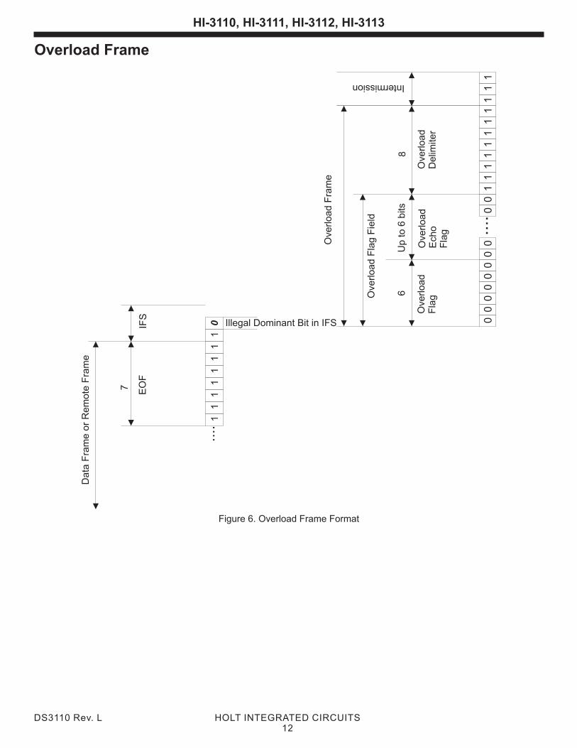
Overload Frame
Figure 6. Overload Frame Format
7 EO
F
11
11
11
11
IFS
....
0
Da
ta F
ram
e o
r R
em
ote
Fra
me
Illegal Dominant Bit in IFS
....
68
Ove
rlo
ad
Fra
me
Up
to
6 b
its
Ove
rlo
ad
E
cho
F
lag
Ove
rlo
ad
F
lag
Ove
rlo
ad
D
elim
iter
00
00
00
00
00
11
11
11
11
Ove
rlo
ad
Fla
g F
ield
11
1
Intermission
HI-3110, HI-3111, HI-3112, HI-3113
DS3110 Rev. L12
HOLT INTEGRATED CIRCUITS
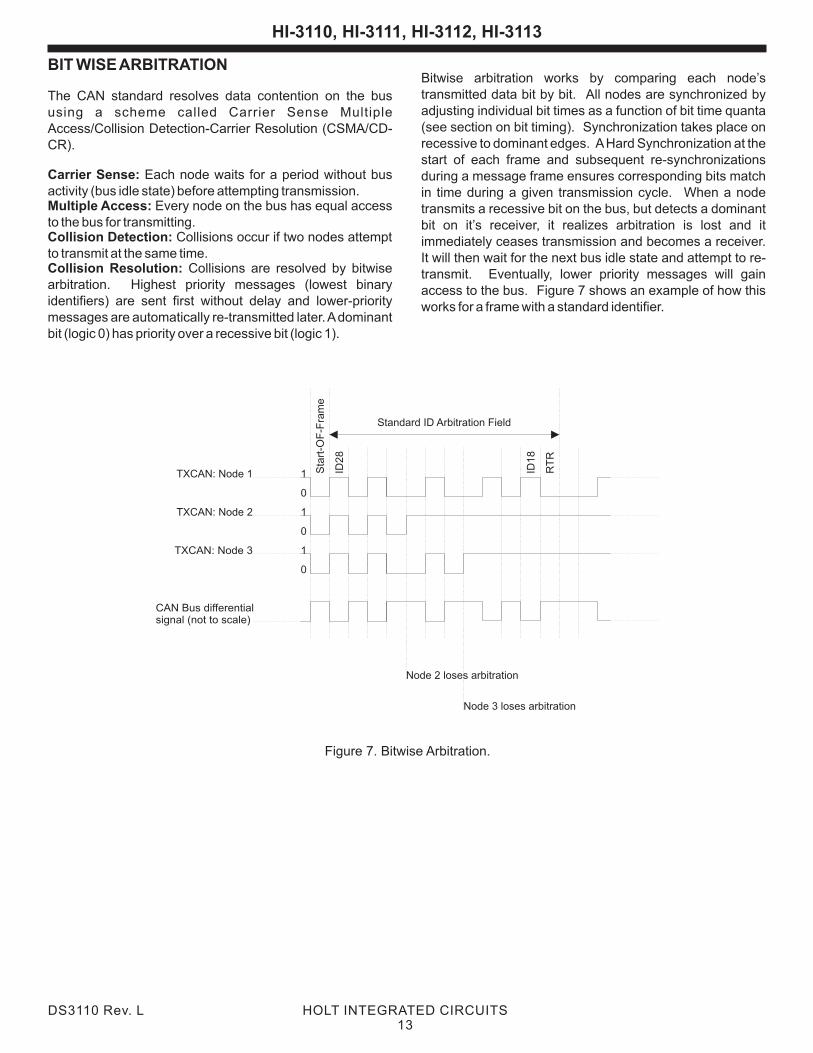
BIT WISE ARBITRATIONBitwise arbitration works by comparing each node’s transmitted data bit by bit. All nodes are synchronized by The CAN standard resolves data contention on the bus adjusting individual bit times as a function of bit time quanta using a scheme called Carrier Sense Multiple (see section on bit timing). Synchronization takes place on Access/Collision Detection-Carrier Resolution (CSMA/CD-recessive to dominant edges. A Hard Synchronization at the CR). start of each frame and subsequent re-synchronizations
Carrier Sense: Each node waits for a period without bus during a message frame ensures corresponding bits match activity (bus idle state) before attempting transmission. in time during a given transmission cycle. When a node Multiple Access: Every node on the bus has equal access transmits a recessive bit on the bus, but detects a dominant to the bus for transmitting. bit on it’s receiver, it realizes arbitration is lost and it Collision Detection: Collisions occur if two nodes attempt immediately ceases transmission and becomes a receiver. to transmit at the same time. It will then wait for the next bus idle state and attempt to re-Collision Resolution: Collisions are resolved by bitwise transmit. Eventually, lower priority messages will gain arbitration. Highest priority messages (lowest binary access to the bus. Figure 7 shows an example of how this identifiers) are sent first without delay and lower-priority works for a frame with a standard identifier. messages are automatically re-transmitted later. A dominant bit (logic 0) has priority over a recessive bit (logic 1).
Figure 7. Bitwise Arbitration.
TXCAN: Node 1
TXCAN: Node 2
TXCAN: Node 3
CAN Bus differential signal (not to scale)
Node 2 loses arbitration
Node 3 loses arbitration
Sta
rt-O
F-F
ram
e
Standard ID Arbitration Field
RT
R
ID18
ID28
1
0
1
0
1
0
HI-3110, HI-3111, HI-3112, HI-3113
DS3110 Rev. L13
HOLT INTEGRATED CIRCUITS
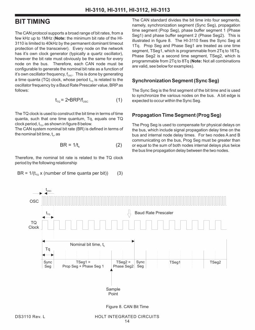
The CAN standard divides the bit time into four segments, BIT TIMINGnamely, synchronization segment (Sync Seg), propagation time segment (Prop Seg), phase buffer segment 1 (Phase
The CAN protocol supports a broad range of bit rates, from a Seg1) and phase buffer segment 2 (Phase Seg2). This is
few kHz up to 1MHz (Note: the minimum bit rate of the HI-illustrated in figure 8. The HI-3110 fixes the Sync Seg at
3110 is limited to 40kHz by the permanent dominant timeout 1Tq. Prop Seg and Phase Seg1 are treated as one time
protection of the transceiver). Every node on the network segment, TSeg1, which is programmable from 2Tq to 16Tq.
has it’s own clock generator (typically a quartz oscillator), Phase Seg2 is a second time segment, TSeg2, which is
however the bit rate must obviously be the same for every programmable from 2Tq to 8Tq (Note: Not all combinations
node on the bus. Therefore, each CAN node must be are valid, see below for examples).
configurable to generate the nominal bit rate as a function of it’s own oscillator frequency, f . This is done by generating OSC
a time quanta (TQ) clock, whose period t is related to the TQ Synchronization Segment (Sync Seg)oscillator frequency by a Baud Rate Prescaler value, BRP as follows: The Sync Seg is the first segment of the bit time and is used
to synchronize the various nodes on the bus. A bit edge is expected to occur within the Sync Seg.
The TQ clock is used to construct the bit time in terms of time Propagation Time Segment (Prog Seg)quanta, such that one time quantum, Tq, equals one TQ clock period, t , as shown in figure 8 below. TQ The Prog Seg is used to compensate for physical delays on The CAN system nominal bit rate (BR) is defined in terms of the bus, which include signal propagation delay time on the the nominal bit time, t , as b bus and internal node delay times. For two nodes A and B
communicating on the bus, Prog Seg must be greater than or equal to the sum of both nodes internal delays plus twice the bus line propagation delay between the two nodes.
Therefore, the nominal bit rate is related to the TQ clock period by the following relationship
BR = 1/t (2)b
BR = 1/(t x (number of time quanta per bit)) (3)TQ
t = BRP/f (1) TQ OSC2•
Figure 8. CAN Bit Time
tTQ
tOSC
OSC
TQ Clock
Baud Rate Prescaler
Sample Point
Tq
TSeg1 = Prop Seg + Phase Seg 1
TSeg2 = Phase Seg2
SyncSeg
Nominal bit time, tb
TSeg1 TSeg2SyncSeg
HI-3110, HI-3111, HI-3112, HI-3113
DS3110 Rev. L14
HOLT INTEGRATED CIRCUITS
frame. Phase Buffer Segment 1 and Phase Buffer Segment 2 (Phase Seg1 and Phase Seg2)
Re-synchronization results in the shortening or lengthening of the bit time such that the position of the The phase buffer segments are used to compensate for sample point is shifted with respect to the edge causing the phase errors on the bus. Phase Seg1 can be lengthened or re-synchronization. For e > 0, Phase Seg 1 is lengthened by Phase Seg2 can be shortened duringthe re-synchronization the magnitude of the phase error, up to a maximum of SJW. bit period automatically by the HI-3110 so that the bit time For e < 0, Phase Seg 2 is shortened by the magnitude of the can be adjusted to account for phase errors. The upper limit phase error, up to a maximum of SJW. by which the lengthening ( or shortening) can occur is set by
the re-synchronization jump width (SJW), explained in more detail below.
Examples
1) CAN bit rate (BR) = 125kHz, f = 12MHz. OSCSample PointAssume sample point (at end of TSeg1) will occur at 75% of bit time. Hence, for Sync Seg = 1Tq, TSeg1 = 5 Tq and The sample point is the point in the bit time at which the bit TSeg2 = 2Tq. Therefore, total bit time will be 8Tq. Chose logic level is interpreted. It is located at the end of Phase SJW = 1Tq.Seg1. The HI-3110 also allows three sample points to be For 125kHz, the bit time needs to be 1/125kHz = 8µs.
taken. In this case, two other sample points are taken prior Hence, 1Tq = 1µs. Using equation (1) => BRP = 6.
to the end of Phase Seg1 (at one-half TQ intervals) and the value of the bit is determined by a majority decision. Three 2) CAN bit rate (BR) = 1MHz, f = 32MHz. OSCsample points are typically only used at low bit rates. Note: Assume sample point (at end of TSeg1) will occur at 75% of ARINC 825 states that there shall be only one sample per bit, bit time. For Sync Seg = 1Tq, then TSeg1 = 11Tq and TSeg2 taken at the end of Phase Seg1. = 4Tq. Therefore, total bit time will be 16Tq. Chose SJW =
1Tq.The time required for the logic to determine the bit level of a
For 1MHz, the bit time needs to be 1/1MHz = 1µs. Hence, sampled bit is known as the information processing time
1Tq = 62.5ns. Using equation (1) => BRP = 1. (IPT). According to the standard, IPT can be up to 2Tq. Since Phase Seg2 occurs after the sample point, Phase Note: Choosing the sample point at 75% of the bit time is a Seg2 must be greater than or equal to the worst case IPT requirement of ARINC 825. The oscillator frequency must (2Tq). be chosen such that a valid value of BRP (integer) can
generate the TQ clock (e.g. in example 2 above, using a lower oscillator frequency than 32MHz results in BRP < 1).
Phase Errors (e)
If a bit edge occurs within the Sync Seg as expected, there is no phase error (e = 0). However, if an edge occurs outside Sync Seg, a phase error is deemed to have occurred. If the edge occurs after Sync Seg (edge occurs “late”), the phase error is positive (e > 0), whereas if the edge occurs before Sync Seg (edge occurs “early”), the phase error is negative (e < 0).
Synchronization
Synchronization is carried out only on recessive-to-dominant bit edges and is used to ensure the bit times of all nodes on the bus are synchronized. This is necessary for arbitration and message acknowledgment to function properly. Only one synchronization can occur per bit time.
Hard synchronizationSync Seg, regardless of the phase error. Hard synchronization only occurs on reception of the start of a
forces the bit edge to lie within the
HI-3110, HI-3111, HI-3112, HI-3113
DS3110 Rev. L15
HOLT INTEGRATED CIRCUITS
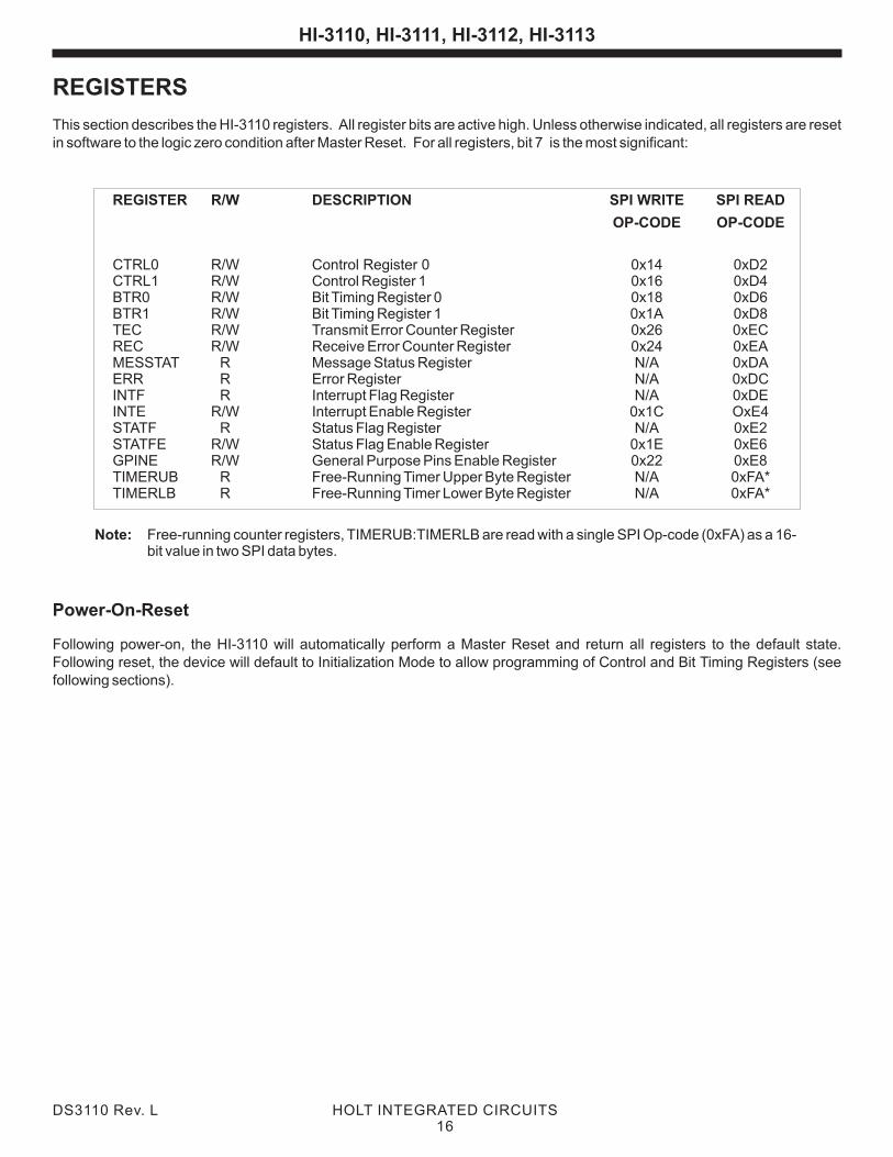
REGISTER R/W DESCRIPTION SPI WRITE SPI READ
OP-CODE OP-CODE
CTRL1 R/W Control Register 1 0x16 0xD4BTR0 R/W Bit Timing Register 0 0x18 0xD6BTR1 R/W Bit Timing Register 1 0x1A 0xD8TEC R/W Transmit Error Counter Register 0x26 0xECREC R/W Receive Error Counter Register 0x24 0xEAMESSTAT R Message Status Register N/A 0xDAERR R Error Register N/A 0xDCINTF R Interrupt Flag Register N/A 0xDEINTE R/W Interrupt Enable Register 0x1C OxE4STATF R Status Flag Register N/A 0xE2STATFE R/W Status Flag Enable Register 0x1E 0xE6GPINE R/W General Purpose Pins Enable Register 0x22 0xE8TIMERUB R Free-Running Timer Upper Byte Register N/A 0xFA*TIMERLB R Free-Running Timer Lower Byte Register N/A 0xFA*
CTRL0 R/W Control Register 0 0x14 0xD2
REGISTERS
This section describes the HI-3110 registers. All register bits are active high. Unless otherwise indicated, all registers are reset in software to the logic zero condition after Master Reset. For all registers, bit 7 is the most significant:
Note: bit value in two SPI data bytes.Free-running counter registers, TIMERUB:TIMERLB are read with a single SPI Op-code (0xFA) as a 16-
Power-On-Reset
Following power-on, the HI-3110 will automatically perform a Master Reset and return all registers to the default state. Following reset, the device will default to Initialization Mode to allow programming of Control and Bit Timing Registers (see following sections).
HI-3110, HI-3111, HI-3112, HI-3113
DS3110 Rev. L16
HOLT INTEGRATED CIRCUITS
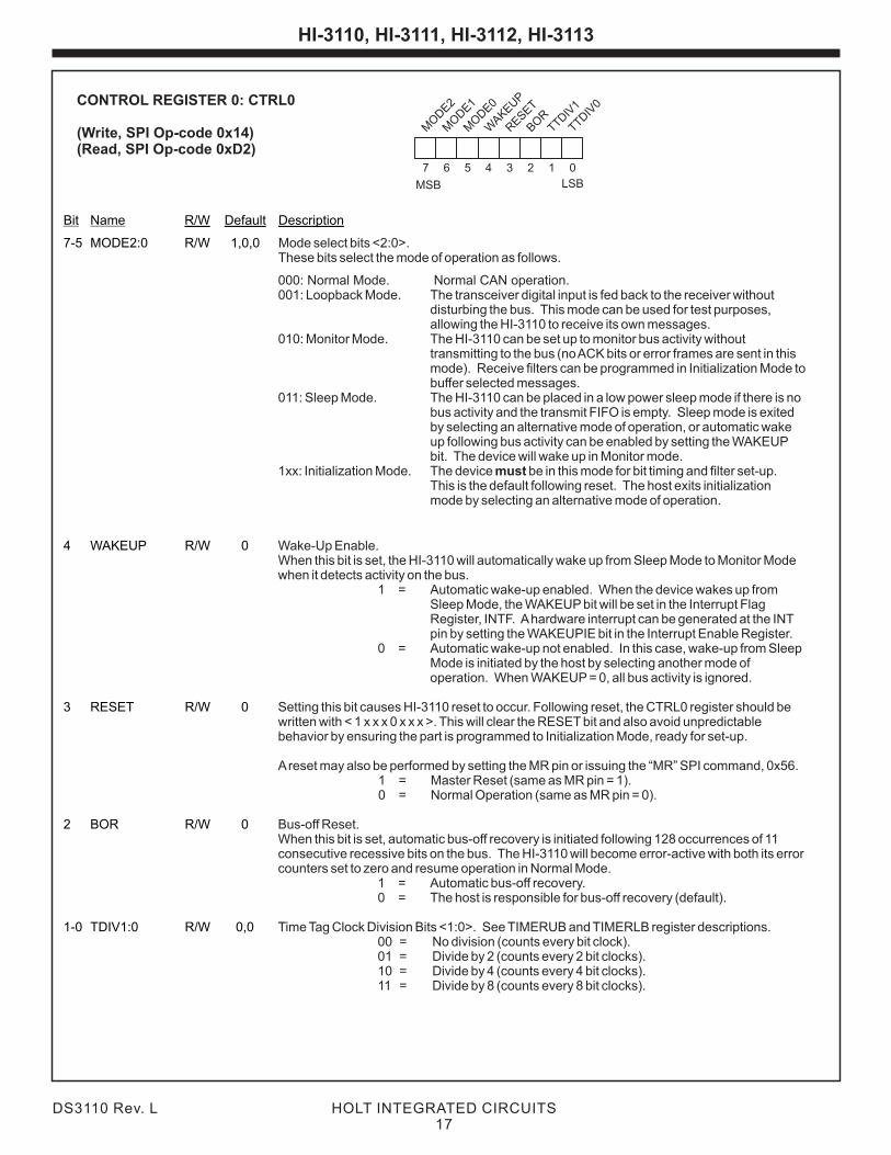
Bit Name R/W Default Description
7-5 MODE2:0
4 WAKEUP R/W 0
3 RESET R/W 0
2 BOR R/W 0
1-0 TDIV1:0 R/W 0,0
R/W 1,0,0 Mode select bits <2:0>. These bits select the mode of operation as follows.
000: Normal Mode. Normal CAN operation. 001: Loopback Mode. The transceiver digital input is fed back to the receiver without
disturbing the bus. This mode can be used for test purposes, allowing the HI-3110 to receive its own messages.
010: Monitor Mode. The HI-3110 can be set up to monitor bus activity without transmitting to the bus (no ACK bits or error frames are sent in this mode). Receive filters can be programmed in Initialization Mode to buffer selected messages.
011: Sleep Mode. The HI-3110 can be placed in a low power sleep mode if there is no bus activity and the transmit FIFO is empty. Sleep mode is exited by selecting an alternative mode of operation, or automatic wake up following bus activity can be enabled by setting the WAKEUP bit. The device will wake up in Monitor mode.
1xx: Initialization Mode. The device must be in this mode for bit timing and filter set-up. This is the default following reset. The host exits initialization mode by selecting an alternative mode of operation.
Wake-Up Enable. When this bit is set, the HI-3110 will automatically wake up from Sleep Mode to Monitor Modewhen it detects activity on the bus.
1 = Automatic wake-up enabled. When the device wakes up from Sleep Mode, the WAKEUP bit will be set in the Interrupt Flag Register, INTF. A hardware interrupt can be generated at the INT pin by setting the WAKEUPIE bit in the Interrupt Enable Register.
0 = Automatic wake-up not enabled. In this case, wake-up from Sleep Mode is initiated by the host by selecting another mode of operation. When WAKEUP = 0, all bus activity is ignored.
Setting this bit causes HI-3110 reset to occur. Following reset, the CTRL0 register should be written with < 1 x x x 0 x x x >. This will clear the RESET bit and also avoid unpredictable behavior by ensuring the part is programmed to Initialization Mode, ready for set-up.
A reset may also be performed by setting the MR pin or issuing the “MR” SPI command, 0x56. 1 = Master Reset (same as MR pin = 1). 0 = Normal Operation (same as MR pin = 0).
Bus-off Reset. When this bit is set, automatic bus-off recovery is initiated following 128 occurrences of 11 consecutive recessive bits on the bus. The HI-3110 will become error-active with both its error counters set to zero and resume operation in Normal Mode.
1 = Automatic bus-off recovery.0 = The host is responsible for bus-off recovery (default).
Time Tag Clock Division Bits <1:0>. See TIMERUB and TIMERLB register descriptions. 00 = No division (counts every bit clock).01 = Divide by 2 (counts every 2 bit clocks). 10 = Divide by 4 (counts every 4 bit clocks). 11 = Divide by 8 (counts every 8 bit clocks).
7 6 5 4 3 2 1 0
MSB LSB
WAKEU
P
RESET
BOR
TTDIV
1
TTDIV
0
MODE0
MODE1
MODE2CONTROL REGISTER 0: CTRL0
(Write, SPI Op-code 0x14)(Read, SPI Op-code 0xD2)
HI-3110, HI-3111, HI-3112, HI-3113
DS3110 Rev. L17
HOLT INTEGRATED CIRCUITS
Bit Name R/W Default Description
7 TXEN R/W 0
6 TX1M R/W 0
5 OSM R/W 0
4 FILTON R/W 0
3 OSCOFF R/W 0
2 Not used R/W 0
1-0 CLKDIV1:0 R/W 00
Transmission Enable. This bit is logically ORed with the TXEN pin. When this bit is asserted, each message in the FIFO will be sequentially loaded to the transmit buffer and sent if the bus is available. If this bit is not set, a transmission can be enabled by either the TXEN pin or the TX1M bit. If the TXEN pin is pulled low during a transmission, the current message being transmitted will be completed. Any additional messages in the FIFO will not be transmitted.
1 = Enable transmission and send any messages in FIFO (until empty if TXEN is held set).
0 = Wait for transmission enable or TX1M bit set before sending next message in FIFO.
Enable transmission of only next message. This bit is applicable only if TXEN = 0. It is reset automatically upon completion of a successful transmission or by initiation of transmission if the OSM bit is set.
1 = Enable transmission of only next message in FIFO when TXEN = 0. 0 = Wait for transmission enable or TX1M bit set before sending next
message in FIFO.
One-Shot Mode Enable. OSM is intended to be used ONLY with the TX1M bit. If OSM is enabled and TX1M is set, the controller transmits only once and does not attempt re-transmission upon loss of arbitration or error. This feature is necessary to support the implementation of fixed time slots in the Time-Triggered CAN standard (TTCAN). Note: Un-transmitted messages will remain in the FIFO. If a new message is required on the next transmission cycle, the user must first clear the FIFO with SPI command 0x54 and then reload the new message.
1 = Enable one-shot mode. 0 = Messages will re-transmit according to CAN protocol.
Filter on enable. This bit is set to turn on the HI-3110 CAN ID filtering mechanism. The default after reset is FILTON = 0, meaning filtering is turned off and every valid CAN message is accepted into the receive FIFO. Note: The device must be in initialization mode in order to program the acceptance filters and masks.
1 = Enable CAN ID filtering. 0 = No CAN ID filtering (every valid message accepted into
receive FIFO).
Oscillator off. This bit should be set to a one if an external clock is used. In this case the external clock is connected to the OSCIN pin and OSCOUT should be left floating.
1 = Shuts off external OSCOUT pin.0 = OSCOUT pin enabled.
External CLKOUT division bits <1:0>00: Divide by 1.01: Divide by 2. 10: Divide by 4. 11: Divide by 8.
7 6 5 4 3 2 1 0
MSB LSB
FILTO
N
OSC
OFF
- CLK
DIV
1
CLK
DIV
0
OSM
TX1M
TXENCONTROL REGISTER 1: CTRL1
(Write, SPI Op-code 0x16)(Read, SPI Op-code 0xD4)
HI-3110, HI-3111, HI-3112, HI-3113
DS3110 Rev. L18
HOLT INTEGRATED CIRCUITS
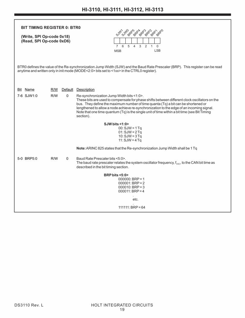
BTR0 defines the value of the Re-synchronization Jump Width (SJW) and the Baud Rate Prescaler (BRP). This register can be read anytime and written only in init mode (MODE<2:0> bits set to <1xx> in the CTRL0 register).
Re-synchronization Jump Width bits <1:0>. These bits are used to compensate for phase shifts between different clock oscillators on the bus. They define the maximum number of time quanta (Tq) a bit can be shortened or lengthened to allow a node achieve re-synchronization to the edge of an incoming signal. Note that one time quantum (Tq) is the single unit of time within a bit time (see Bit Timing section).
SJW bits <1:0>00: SJW = 1 Tq01: SJW = 2 Tq10: SJW = 3 Tq11: SJW = 4 Tq
Note: ARINC 825 states that the Re-synchronization Jump Width shall be 1 Tq
Baud Rate Prescaler bits <5:0>. The baud rate prescaler relates the system oscillator frequency, f , to the CAN bit time as OSC
described in the bit timing section.
BRP bits <5:0>000000: BRP = 1000001: BRP = 2000010: BRP = 3000011: BRP = 4
.etc..
111111: BRP = 64
Bit Name R/W Default Description
7-6 SJW1:0 R/W 0
5-0 BRP5:0 R/W 0
7 6 5 4 3 2 1 0
MSB LSB
BRP4
BRP3
BRP2
BRP1
BRP0
BRP5
SJW0
SJW1
BIT TIMING REGISTER 0: BTR0
(Write, SPI Op-code 0x18)(Read, SPI Op-code 0xD6)
HI-3110, HI-3111, HI-3112, HI-3113
DS3110 Rev. L19
HOLT INTEGRATED CIRCUITS
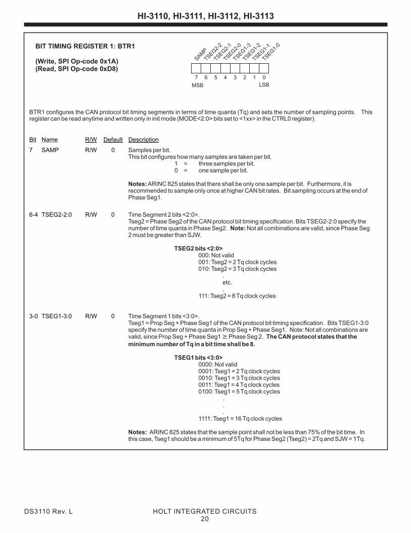
BTR1 configures the CAN protocol bit timing segments in terms of time quanta (Tq) and sets the number of sampling points. This register can be read anytime and written only in init mode (MODE<2:0> bits set to <1xx> in the CTRL0 register).
Samples per bit. This bit configures how many samples are taken per bit.
1 = three samples per bit.0 = one sample per bit.
Notes: ARINC 825 states that there shall be only one sample per bit. Furthermore, it is recommended to sample only once at higher CAN bit rates. Bit sampling occurs at the end of Phase Seg1.
Time Segment 2 bits <2:0>. Tseg2 = Phase Seg2 of the CAN protocol bit timing specification. Bits TSEG2-2:0 specify the number of time quanta in Phase Seg2. Note: Not all combinations are valid, since Phase Seg 2 must be greater than SJW.
TSEG2 bits <2:0>000: Not valid001: Tseg2 = 2 Tq clock cycles010: Tseg2 = 3 Tq clock cycles
.etc..
111: Tseg2 = 8 Tq clock cycles
Time Segment 1 bits <3:0>. Tseg1 = Prop Seg + Phase Seg1 of the CAN protocol bit timing specification. Bits TSEG1-3:0 specify the number of time quanta in Prop Seg + Phase Seg1. Note: Not all combinations are valid, since Prop Seg + Phase Seg1 ³ Phase Seg 2. The CAN protocol states that the minimum number of Tq in a bit time shall be 8.
TSEG1 bits <3:0>0000: Not valid0001: Tseg1 = 2 Tq clock cycles0010: Tseg1 = 3 Tq clock cycles0011: Tseg1 = 4 Tq clock cycles0100: Tseg1 = 5 Tq clock cycles
.
.
.1111: Tseg1 = 16 Tq clock cycles
Notes: ARINC 825 states that the sample point shall not be less than 75% of the bit time. In this case, Tseg1 should be a minimum of 5Tq for Phase Seg2 (Tseg2) = 2Tq and SJW = 1Tq.
Bit Name R/W Default Description
7 SAMP R/W 0
6-4 TSEG2-2:0 R/W 0
3-0 TSEG1-3:0 R/W 0
7 6 5 4 3 2 1 0
MSB LSB
TSEG2-
0
TSEG1-
3
TSEG1-
2
TSEG1-
1
TSEG1-
0
TSEG2-
1
TSEG2-
2
SAMP
BIT TIMING REGISTER 1: BTR1
(Write, SPI Op-code 0x1A)(Read, SPI Op-code 0xD8)
HI-3110, HI-3111, HI-3112, HI-3113
DS3110 Rev. L20
HOLT INTEGRATED CIRCUITS
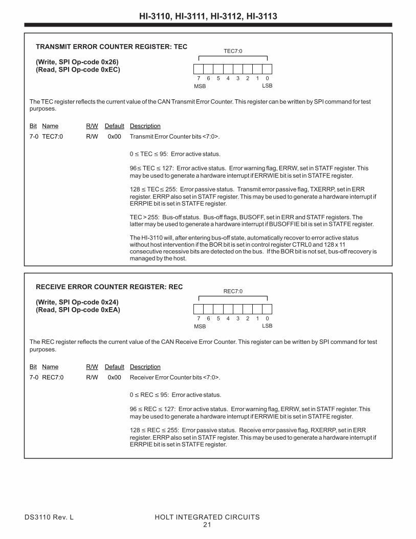
The TEC register reflects the current value of the CAN Transmit Error Counter. This register can be written by SPI command for test purposes.
Transmit Error Counter bits <7:0>.
0 £ TEC £ 95: Error active status.
96£ TEC £ 127: Error active status. Error warning flag, ERRW, set in STATF register. This may be used to generate a hardware interrupt if ERRWIE bit is set in STATFE register.
128 £ TEC£ 255: Error passive status. Transmit error passive flag, TXERRP, set in ERR register. ERRP also set in STATF register. This may be used to generate a hardware interrupt if ERRPIE bit is set in STATFE register.
TEC > 255: Bus-off status. Bus-off flags, BUSOFF, set in ERR and STATF registers. The latter may be used to generate a hardware interrupt if BUSOFFIE bit is set in STATFE register.
The HI-3110 will, after entering bus-off state, automatically recover to error active status without host intervention if the BOR bit is set in control register CTRL0 and 128 x 11 consecutive recessive bits are detected on the bus. If the BOR bit is not set, bus-off recovery is managed by the host.
Bit Name R/W Default Description
7-0 TEC7:0 R/W 0x00
7 6 5 4 3 2 1 0
MSB LSB
TRANSMIT ERROR COUNTER REGISTER: TEC
(Write, SPI Op-code 0x26)(Read, SPI Op-code 0xEC)
TEC7:0
The REC register reflects the current value of the CAN Receive Error Counter. This register can be written by SPI command for test purposes.
Receiver Error Counter bits <7:0>.
0 £ REC £ 95: Error active status.
96 £ REC £ 127: Error active status. Error warning flag, ERRW, set in STATF register. This may be used to generate a hardware interrupt if ERRWIE bit is set in STATFE register.
128 £ REC £ 255: Error passive status. Receive error passive flag, RXERRP, set in ERR register. ERRP also set in STATF register. This may be used to generate a hardware interrupt if ERRPIE bit is set in STATFE register.
Bit Name R/W Default Description
7-0 REC7:0 R/W 0x00
7 6 5 4 3 2 1 0
MSB LSB
RECEIVE ERROR COUNTER REGISTER: REC
(Write, SPI Op-code 0x24)(Read, SPI Op-code 0xEA)
REC7:0
HI-3110, HI-3111, HI-3112, HI-3113
DS3110 Rev. L21
HOLT INTEGRATED CIRCUITS
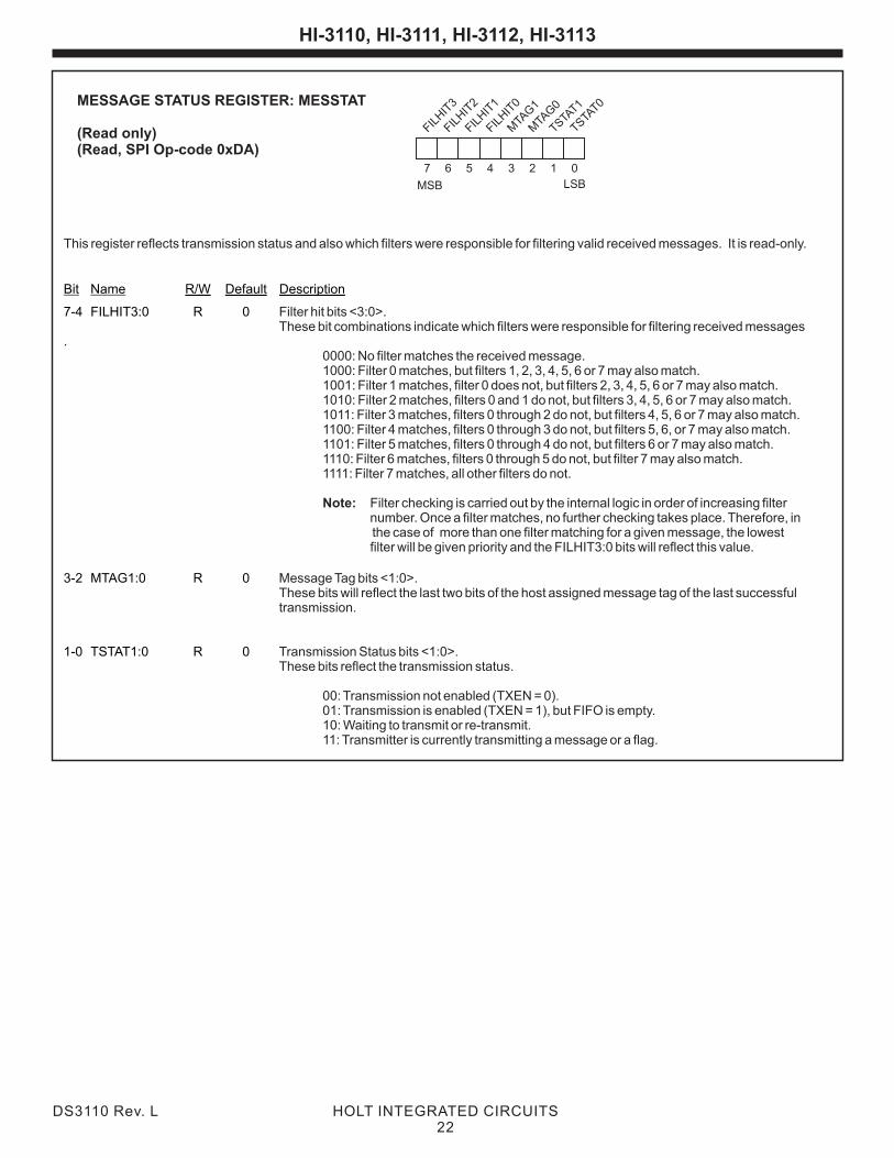
This register reflects transmission status and also which filters were responsible for filtering valid received messages. It is read-only.
Filter hit bits <3:0>. These bit combinations indicate which filters were responsible for filtering received messages
. 0000: No filter matches the received message.1000: Filter 0 matches, but filters 1, 2, 3, 4, 5, 6 or 7 may also match.1001: Filter 1 matches, filter 0 does not, but filters 2, 3, 4, 5, 6 or 7 may also match.1010: Filter 2 matches, filters 0 and 1 do not, but filters 3, 4, 5, 6 or 7 may also match.1011: Filter 3 matches, filters 0 through 2 do not, but filters 4, 5, 6 or 7 may also match.1100: Filter 4 matches, filters 0 through 3 do not, but filters 5, 6, or 7 may also match.1101: Filter 5 matches, filters 0 through 4 do not, but filters 6 or 7 may also match.1110: Filter 6 matches, filters 0 through 5 do not, but filter 7 may also match.1111: Filter 7 matches, all other filters do not.
Note: Filter checking is carried out by the internal logic in order of increasing filter number. Once a filter matches, no further checking takes place. Therefore, in the case of more than one filter matching for a given message, the lowest filter will be given priority and the FILHIT3:0 bits will reflect this value.
Message Tag bits <1:0>. These bits will reflect the last two bits of the host assigned message tag of the last successful transmission.
Transmission Status bits <1:0>. These bits reflect the transmission status.
00: Transmission not enabled (TXEN = 0).01: Transmission is enabled (TXEN = 1), but FIFO is empty.10: Waiting to transmit or re-transmit. 11: Transmitter is currently transmitting a message or a flag.
Bit Name R/W Default Description
7-4 FILHIT3:0 R 0
3-2 MTAG1:0 R 0
1-0 TSTAT1:0 R 0
7 6 5 4 3 2 1 0
MSB LSB
FILHIT
0
MTA
G1
MTA
G0
TSTAT1
TSTAT0
FILHIT
1
FILHIT
2
FILHIT
3MESSAGE STATUS REGISTER: MESSTAT
(Read only)(Read, SPI Op-code 0xDA)
HI-3110, HI-3111, HI-3112, HI-3113
DS3110 Rev. L22
HOLT INTEGRATED CIRCUITS
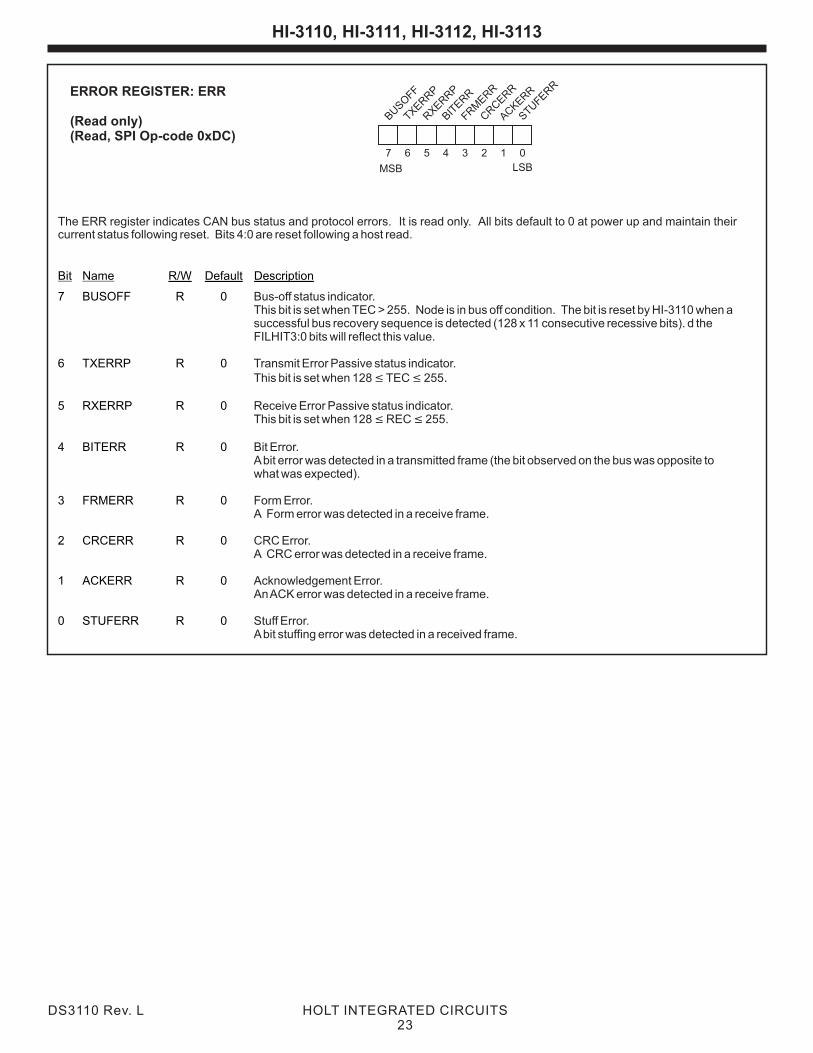
The ERR register indicates CAN bus status and protocol errors. It is read only. All bits default to 0 at power up and maintain their current status following reset. Bits 4:0 are reset following a host read.
Bus-off status indicator. This bit is set when TEC > 255. Node is in bus off condition. The bit is reset by HI-3110 when a successful bus recovery sequence is detected (128 x 11 consecutive recessive bits). d the FILHIT3:0 bits will reflect this value.
Transmit Error Passive status indicator. This bit is set when 128 £ TEC £ 255
Receive Error Passive status indicator. This bit is set when 128 £ REC £ 255.
Bit Error. A bit error was detected in a transmitted frame (the bit observed on the bus was opposite to what was expected).
Form Error. A Form error was detected in a receive frame.
CRC Error. A CRC error was detected in a receive frame.
Acknowledgement Error. An ACK error was detected in a receive frame.
Stuff Error. A bit stuffing error was detected in a received frame.
Bit Name R/W Default Description
7 BUSOFF R 0
6 TXERRP R 0
5 RXERRP R 0
4 BITERR R 0
3 FRMERR R 0
2 CRCERR R 0
1 ACKERR R 0
0 STUFERR R 0
.
7 6 5 4 3 2 1 0
MSB LSB
BITER
R
FRM
ERR
CRCER
R
ACKER
R
STUFER
R
RXER
RP
TXERRP
BUSO
FFERROR REGISTER: ERR
(Read only)(Read, SPI Op-code 0xDC)
HI-3110, HI-3111, HI-3112, HI-3113
DS3110 Rev. L23
HOLT INTEGRATED CIRCUITS
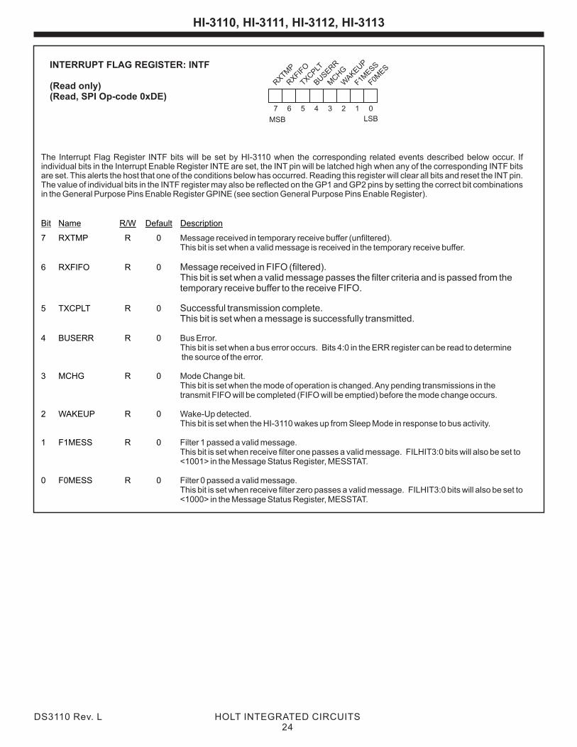
The Interrupt Flag Register INTF bits will be set by HI-3110 when the corresponding related events described below occur. If individual bits in the Interrupt Enable Register INTE are set, the INT pin will be latched high when any of the corresponding INTF bits are set. This alerts the host that one of the conditions below has occurred. Reading this register will clear all bits and reset the INT pin. The value of individual bits in the INTF register may also be reflected on the GP1 and GP2 pins by setting the correct bit combinations in the General Purpose Pins Enable Register GPINE (see section General Purpose Pins Enable Register).
Message received in temporary receive buffer (unfiltered). This bit is set when a valid message is received in the temporary receive buffer.
Message received in FIFO (filtered). This bit is set when a valid message passes the filter criteria and is passed from the temporary receive buffer to the receive FIFO.
Successful transmission complete. This bit is set when a message is successfully transmitted.
Bus Error. This bit is set when a bus error occurs. Bits 4:0 in the ERR register can be read to determine the source of the error.
Mode Change bit. This bit is set when the mode of operation is changed. Any pending transmissions in the transmit FIFO will be completed (FIFO will be emptied) before the mode change occurs.
Wake-Up detected. This bit is set when the HI-3110 wakes up from Sleep Mode in response to bus activity.
Filter 1 passed a valid message. This bit is set when receive filter one passes a valid message. FILHIT3:0 bits will also be set to <1001> in the Message Status Register, MESSTAT.
Filter 0 passed a valid message. This bit is set when receive filter zero passes a valid message. FILHIT3:0 bits will also be set to <1000> in the Message Status Register, MESSTAT.
Bit Name R/W Default Description
7 RXTMP R 0
6 RXFIFO R 0
5 TXCPLT R 0
4 BUSERR R 0
3 MCHG R 0
2 WAKEUP R 0
1 F1MESS R 0
0 F0MESS R 0
7 6 5 4 3 2 1 0
MSB LSB
BUSER
R
MCHG
WAKEU
P
F1MESS
F0MES
TXCPLT
RXFIF
O
RXTM
PINTERRUPT FLAG REGISTER: INTF
(Read only)(Read, SPI Op-code 0xDE)
HI-3110, HI-3111, HI-3112, HI-3113
DS3110 Rev. L24
HOLT INTEGRATED CIRCUITS
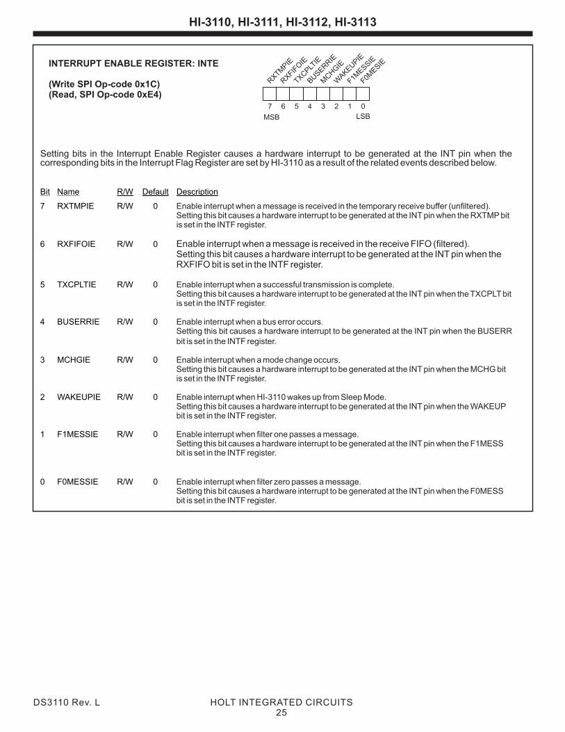
Setting bits in the Interrupt Enable Register causes a hardware interrupt to be generated at the INT pin when the corresponding bits in the Interrupt Flag Register are set by HI-3110 as a result of the related events described below.
Enable interrupt when a message is received in the temporary receive buffer (unfiltered). Setting this bit causes a hardware interrupt to be generated at the INT pin when the RXTMP bit is set in the INTF register.
Enable interrupt when a message is received in the receive FIFO (filtered). Setting this bit causes a hardware interrupt to be generated at the INT pin when the RXFIFO bit is set in the INTF register.
Enable interrupt when a successful transmission is complete. Setting this bit causes a hardware interrupt to be generated at the INT pin when the TXCPLT bit is set in the INTF register.
Enable interrupt when a bus error occurs. Setting this bit causes a hardware interrupt to be generated at the INT pin when the BUSERR bit is set in the INTF register.
Enable interrupt when a mode change occurs. Setting this bit causes a hardware interrupt to be generated at the INT pin when the MCHG bit is set in the INTF register.
Enable interrupt when HI-3110 wakes up from Sleep Mode.Setting this bit causes a hardware interrupt to be generated at the INT pin when the WAKEUP bit is set in the INTF register.
Enable interrupt when filter one passes a message. Setting this bit causes a hardware interrupt to be generated at the INT pin when the F1MESS bit is set in the INTF register.
Enable interrupt when filter zero passes a message. Setting this bit causes a hardware interrupt to be generated at the INT pin when the F0MESS bit is set in the INTF register.
Bit Name R/W Default Description
7 RXTMPIE R/W 0
6 RXFIFOIE R/W 0
5 TXCPLTIE R/W 0
4 BUSERRIE R/W 0
3 MCHGIE R/W 0
2 WAKEUPIE R/W 0
1 F1MESSIE R/W 0
0 F0MESSIE R/W 0
7 6 5 4 3 2 1 0
MSB LSB
BUSER
RIE
MCHGIE
WAKEU
PIE
F1MESSIE
F0MESIE
TXCPLT
IE
RXFIF
OIE
RXTM
PIEINTERRUPT ENABLE REGISTER: INTE
(Write SPI Op-code 0x1C)(Read, SPI Op-code 0xE4)
HI-3110, HI-3111, HI-3112, HI-3113
DS3110 Rev. L25
HOLT INTEGRATED CIRCUITS
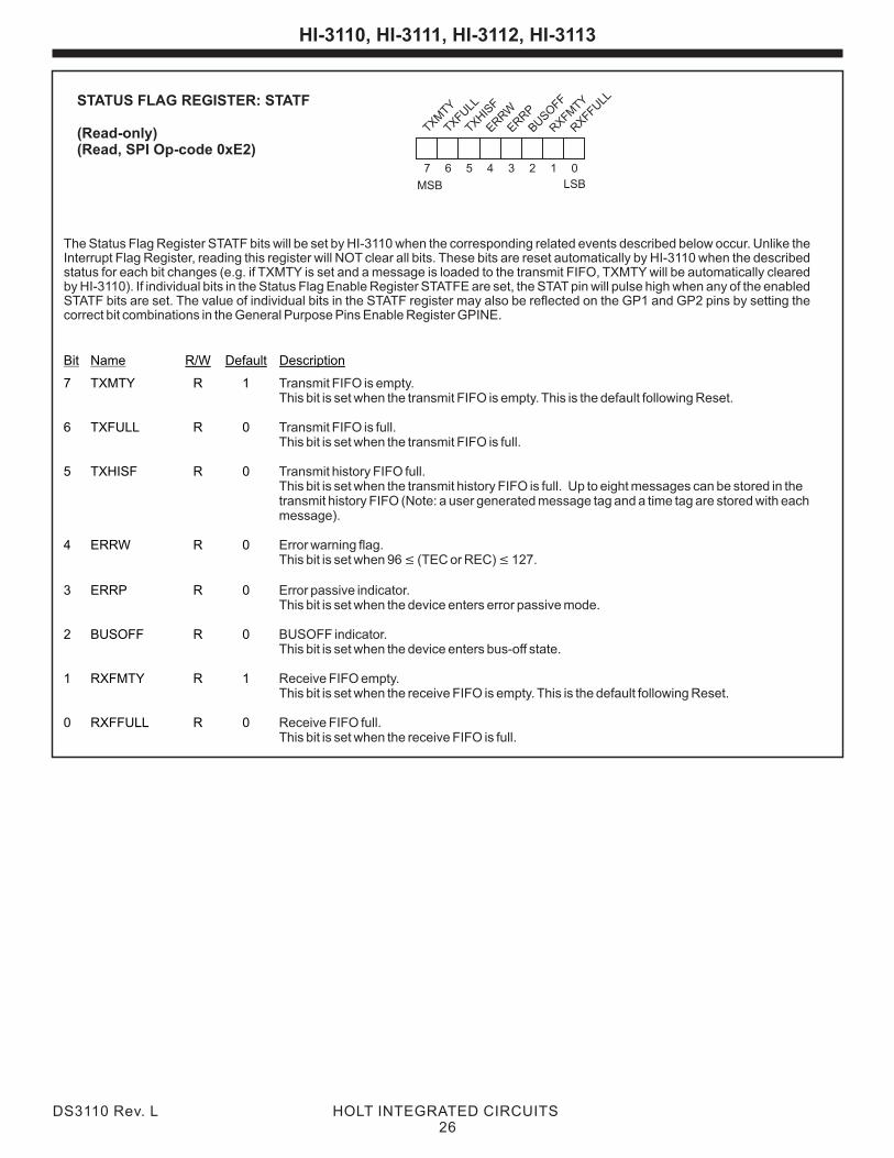
The Status Flag Register STATF bits will be set by HI-3110 when the corresponding related events described below occur. Unlike the Interrupt Flag Register, reading this register will NOT clear all bits. These bits are reset automatically by HI-3110 when the described status for each bit changes (e.g. if TXMTY is set and a message is loaded to the transmit FIFO, TXMTY will be automatically cleared by HI-3110). If individual bits in the Status Flag Enable Register STATFE are set, the STAT pin will pulse high when any of the enabled STATF bits are set. The value of individual bits in the STATF register may also be reflected on the GP1 and GP2 pins by setting the correct bit combinations in the General Purpose Pins Enable Register GPINE.
Transmit FIFO is empty. This bit is set when the transmit FIFO is empty. This is the default following Reset.
Transmit FIFO is full.This bit is set when the transmit FIFO is full.
Transmit history FIFO full. This bit is set when the transmit history FIFO is full. Up to eight messages can be stored in the transmit history FIFO (Note: a user generated message tag and a time tag are stored with each message).
Error warning flag. This bit is set when 96 £ (TEC or REC) £ 127.
Error passive indicator. This bit is set when the device enters error passive mode.
BUSOFF indicator. This bit is set when the device enters bus-off state.
Receive FIFO empty. This bit is set when the receive FIFO is empty. This is the default following Reset.
Receive FIFO full. This bit is set when the receive FIFO is full.
Bit Name R/W Default Description
7 TXMTY R 1
6 TXFULL R 0
5 TXHISF R 0
4 ERRW R 0
3 ERRP R 0
2 BUSOFF R 0
1 RXFMTY R 1
0 RXFFULL R 0
7 6 5 4 3 2 1 0
MSB LSB
ERRW
ERRP
BUSO
FF
RXFM
TY
RXFFU
LL
TXHIS
F
TXFULL
TXMTYSTATUS FLAG REGISTER: STATF
(Read-only)(Read, SPI Op-code 0xE2)
DS3110 Rev. L HOLT INTEGRATED CIRCUITS26
HI-3110, HI-3111, HI-3112, HI-3113
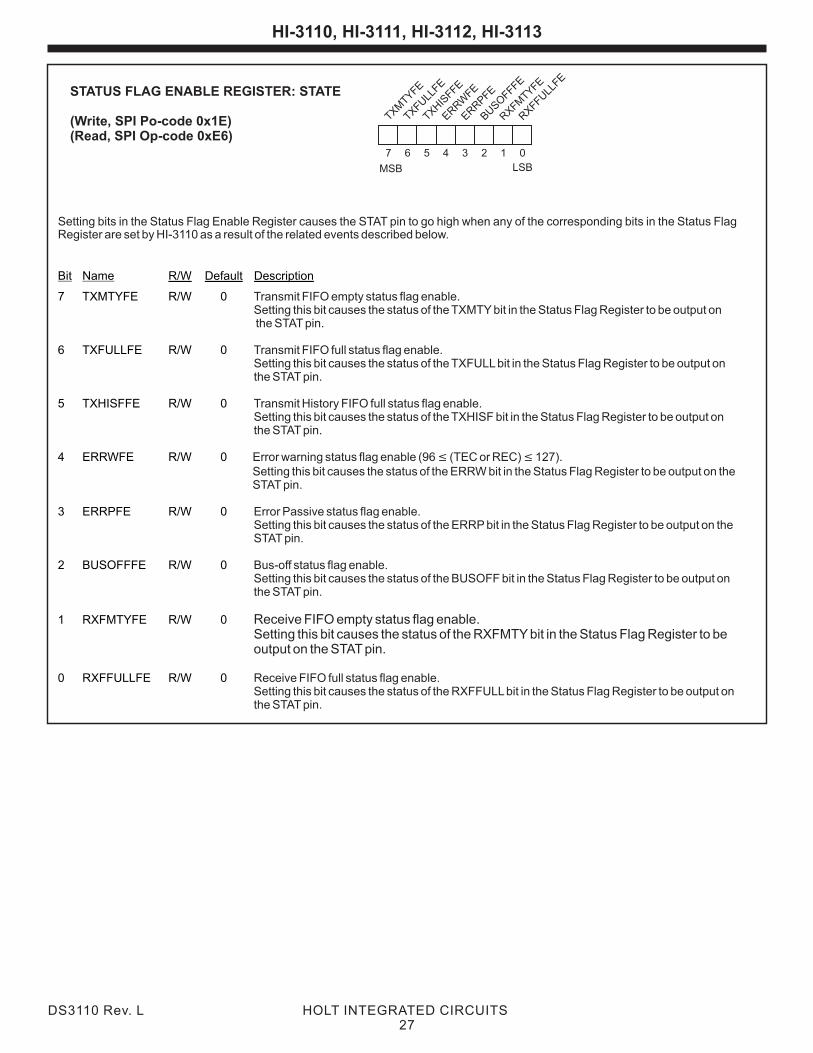
Setting bits in the Status Flag Enable Register causes the STAT pin to go high when any of the corresponding bits in the Status Flag Register are set by HI-3110 as a result of the related events described below.
Transmit FIFO empty status flag enable. Setting this bit causes the status of the TXMTY bit in the Status Flag Register to be output on the STAT pin.
Transmit FIFO full status flag enable. Setting this bit causes the status of the TXFULL bit in the Status Flag Register to be output on the STAT pin.
Transmit History FIFO full status flag enable.Setting this bit causes the status of the TXHISF bit in the Status Flag Register to be output on the STAT pin.
Error warning status flag enable (96 £ (TEC or REC) £ 127).Setting this bit causes the status of the ERRW bit in the Status Flag Register to be output on the STAT pin.
Error Passive status flag enable. Setting this bit causes the status of the ERRP bit in the Status Flag Register to be output on the STAT pin.
Bus-off status flag enable. Setting this bit causes the status of the BUSOFF bit in the Status Flag Register to be output on the STAT pin.
Receive FIFO empty status flag enable. Setting this bit causes the status of the RXFMTY bit in the Status Flag Register to be output on the STAT pin.
Receive FIFO full status flag enable. Setting this bit causes the status of the RXFFULL bit in the Status Flag Register to be output on the STAT pin.
Bit Name R/W Default Description
7 TXMTYFE R/W 0
6 TXFULLFE R/W 0
5 TXHISFFE R/W 0
4 ERRWFE R/W 0
3 ERRPFE R/W 0
2 BUSOFFFE R/W 0
1 RXFMTYFE R/W 0
0 RXFFULLFE R/W 0
7 6 5 4 3 2 1 0
MSB LSB
ERRW
FE
ERRPFE
BUSO
FFFE
RXFM
TYFE
RXFFU
LLFE
TXHIS
FFE
TXFULL
FE
TXMTYFESTATUS FLAG ENABLE REGISTER: STATE
(Write, SPI Po-code 0x1E)(Read, SPI Op-code 0xE6)
DS3110 Rev. L HOLT INTEGRATED CIRCUITS27
HI-3110, HI-3111, HI-3112, HI-3113
DS3110 Rev. L HOLT INTEGRATED CIRCUITS28
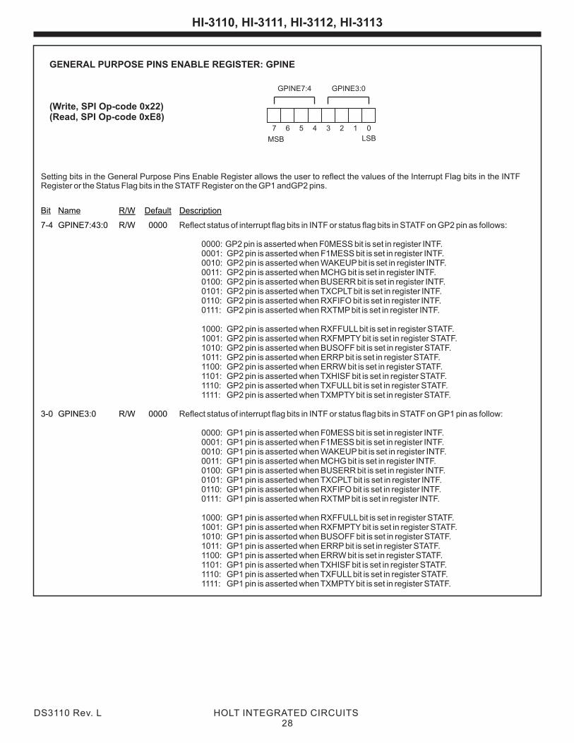
Setting bits in the General Purpose Pins Enable Register allows the user to reflect the values of the Interrupt Flag bits in the INTF Register or the Status Flag bits in the STATF Register on the GP1 andGP2 pins.
Reflect status of interrupt flag bits in INTF or status flag bits in STATF on GP2 pin as follows:
0000: GP2 pin is asserted when F0MESS bit is set in register INTF.0001: GP2 pin is asserted when F1MESS bit is set in register INTF.0010: GP2 pin is asserted when WAKEUP bit is set in register INTF.0011: GP2 pin is asserted when MCHG bit is set in register INTF.0100: GP2 pin is asserted when BUSERR bit is set in register INTF.0101: GP2 pin is asserted when TXCPLT bit is set in register INTF.0110: GP2 pin is asserted when RXFIFO bit is set in register INTF.0111: GP2 pin is asserted when RXTMP bit is set in register INTF.
1000: GP2 pin is asserted when RXFFULL bit is set in register STATF.1001: GP2 pin is asserted when RXFMPTY bit is set in register STATF.1010: GP2 pin is asserted when BUSOFF bit is set in register STATF.1011: GP2 pin is asserted when ERRP bit is set in register STATF.1100: GP2 pin is asserted when ERRW bit is set in register STATF.1101: GP2 pin is asserted when TXHISF bit is set in register STATF.1110: GP2 pin is asserted when TXFULL bit is set in register STATF.1111: GP2 pin is asserted when TXMPTY bit is set in register STATF.
Reflect status of interrupt flag bits in INTF or status flag bits in STATF on GP1 pin as follow:
0000: GP1 pin is asserted when F0MESS bit is set in register INTF.0001: GP1 pin is asserted when F1MESS bit is set in register INTF.0010: GP1 pin is asserted when WAKEUP bit is set in register INTF.0011: GP1 pin is asserted when MCHG bit is set in register INTF.0100: GP1 pin is asserted when BUSERR bit is set in register INTF.0101: GP1 pin is asserted when TXCPLT bit is set in register INTF.0110: GP1 pin is asserted when RXFIFO bit is set in register INTF.0111: GP1 pin is asserted when RXTMP bit is set in register INTF.
1000: GP1 pin is asserted when RXFFULL bit is set in register STATF.1001: GP1 pin is asserted when RXFMPTY bit is set in register STATF.1010: GP1 pin is asserted when BUSOFF bit is set in register STATF.1011: GP1 pin is asserted when ERRP bit is set in register STATF.1100: GP1 pin is asserted when ERRW bit is set in register STATF.1101: GP1 pin is asserted when TXHISF bit is set in register STATF.1110: GP1 pin is asserted when TXFULL bit is set in register STATF.1111: GP1 pin is asserted when TXMPTY bit is set in register STATF.
Bit Name R/W Default Description
7-4 GPINE7:43:0 R/W 0000
3-0 GPINE3:0 R/W 0000
7 6 5 4 3 2 1 0
MSB LSB
GENERAL PURPOSE PINS ENABLE REGISTER: GPINE
(Write, SPI Op-code 0x22)(Read, SPI Op-code 0xE8)
GPINE7:4 GPINE3:0
HI-3110, HI-3111, HI-3112, HI-3113
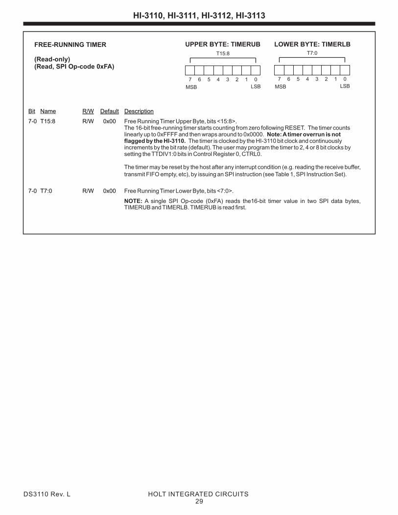
Bit Name R/W Default Description
7-0 T15:8 R/W 0x00
7-0 T7:0 R/W 0x00
Free Running Timer Upper Byte, bits <15:8>. The 16-bit free-running timer starts counting from zero following RESET. The timer counts linearly up to 0xFFFF and then wraps around to 0x0000. Note: A timer overrun is not flagged by the HI-3110. The timer is clocked by the HI-3110 bit clock and continuously increments by the bit rate (default). The user may program the timer to 2, 4 or 8 bit clocks by setting the TTDIV1:0 bits in Control Register 0, CTRL0.
The timer may be reset by the host after any interrupt condition (e.g. reading the receive buffer, transmit FIFO empty, etc), by issuing an SPI instruction (see Table 1, SPI Instruction Set).
Free Running Timer Lower Byte, bits <7:0>.
NOTE: A single SPI Op-code (0xFA) reads the16-bit timer value in two SPI data bytes, TIMERUB and TIMERLB. TIMERUB is read first.
FREE-RUNNING TIMER
(Read-only)(Read, SPI Op-code 0xFA)
7 6 5 4 3 2 1 0
MSB LSB
T15:8
DS3110 Rev. L HOLT INTEGRATED CIRCUITS29
7 6 5 4 3 2 1 0
MSB LSB
T7:0
UPPER BYTE: TIMERUB LOWER BYTE: TIMERLB
HI-3110, HI-3111, HI-3112, HI-3113
MSB LSB
MSB LSBHigh ZHigh Z
CS
SO
SI
0 1 2 3 4 5 6 7SCK (SPI Mode 0)
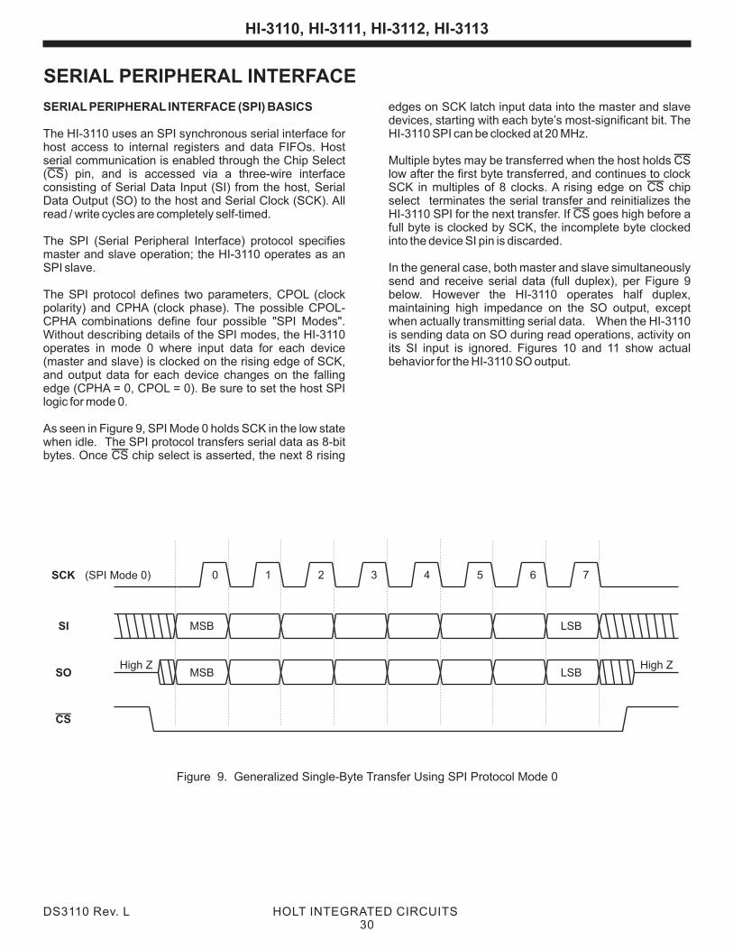
Figure 9. Generalized Single-Byte Transfer Using SPI Protocol Mode 0
SERIAL PERIPHERAL INTERFACE (SPI) BASICS
CSCS
CS
CS
In the general case, both master and slave simultaneously send and receive serial data (full duplex), per Figure 9 below. However the HI-3110 operates half duplex, maintaining high impedance on the SO output, except when actually transmitting serial data. When the HI-3110 is sending data on SO during read operations, activity on its SI input is ignored. Figures 10 and 11 show actual behavior for the HI-3110 SO output.
CS
edges on SCK latch input data into the master and slave devices, starting with each byte’s most-significant bit. The
The HI-3110 uses an SPI synchronous serial interface for HI-3110 SPI can be clocked at 20 MHz. host access to internal registers and data FIFOs. Host serial communication is enabled through the Chip Select Multiple bytes may be transferred when the host holds ( ) pin, and is accessed via a three-wire interface low after the first byte transferred, and continues to clock consisting of Serial Data Input (SI) from the host, Serial SCK in multiples of 8 clocks. A rising edge on chip Data Output (SO) to the host and Serial Clock (SCK). All select terminates the serial transfer and reinitializes the read / write cycles are completely self-timed. HI-3110 SPI for the next transfer. If goes high before a
full byte is clocked by SCK, the incomplete byte clocked The SPI (Serial Peripheral Interface) protocol specifies into the device SI pin is discarded. master and slave operation; the HI-3110 operates as an SPI slave.
The SPI protocol defines two parameters, CPOL (clock polarity) and CPHA (clock phase). The possible CPOL-CPHA combinations define four possible "SPI Modes". Without describing details of the SPI modes, the HI-3110 operates in mode 0 where input data for each device (master and slave) is clocked on the rising edge of SCK, and output data for each device changes on the falling edge (CPHA = 0, CPOL = 0). Be sure to set the host SPI logic for mode 0.
As seen in Figure 9, SPI Mode 0 holds SCK in the low state when idle. The SPI protocol transfers serial data as 8-bit bytes. Once chip select is asserted, the next 8 rising
SERIAL PERIPHERAL INTERFACE
DS3110 Rev. L HOLT INTEGRATED CIRCUITS30
HI-3110, HI-3111, HI-3112, HI-3113
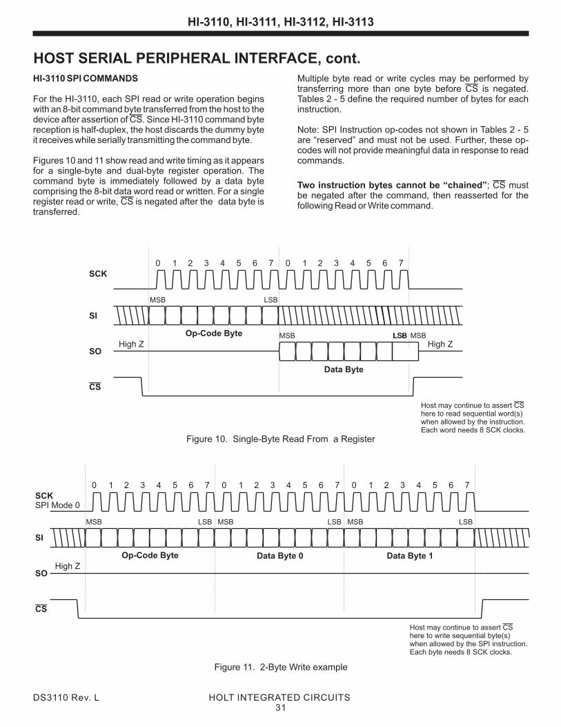
Figure 11. 2-Byte Write example
CS
SO
SI
SCKSPI Mode 0
MSB LSB
0 1 2 3 4 5 6 7
High Z
0 1 2 3 4 5 6 7 0 1 2 3 4 5 6 7
MSB LSB MSB LSB
Data Byte 0 Data Byte 1Op-Code Byte
Host may continue to assert here to write sequential byte(s) when allowed by the SPI instruction.Each byte needs 8 SCK clocks.
CS
Figure 10. Single-Byte Read From a Register
CS
SO
SI
SCK
MSB LSB
0 1 2 3 4 5 6 7
High Z High Z
0 1 2 3 4 5 6 7
MSB LSB MSBLSB
Data Byte
Op-Code Byte
Host may continue to assert here to read sequential word(s) when allowed by the instruction.Each word needs 8 SCK clocks.
CS
HI-3110 SPI COMMANDS Multiple byte read or write cycles may be performed by transferring more than one byte before is negated.
For the HI-3110, each SPI read or write operation begins Tables 2 - 5 define the required number of bytes for each with an 8-bit command byte transferred from the host to the instruction.device after assertion of . Since HI-3110 command byte reception is half-duplex, the host discards the dummy byte Note: SPI Instruction op-codes not shown in Tables 2 - 5 it receives while serially transmitting the command byte. are “reserved” and must not be used. Further, these op-
codes will not provide meaningful data in response to read Figures 10 and 11 show read and write timing as it appears commands.for a single-byte and dual-byte register operation. The command byte is immediately followed by a data byte comprising the 8-bit data word read or written. For a single register read or write, is negated after the data byte is transferred.
CS
CS
Two instruction bytes cannot be “chained” CSbe negated after the command, then reasserted for the
CS following Read or Write command.
; must
HOST SERIAL PERIPHERAL INTERFACE, cont.
DS3110 Rev. L HOLT INTEGRATED CIRCUITS31
HI-3110, HI-3111, HI-3112, HI-3113
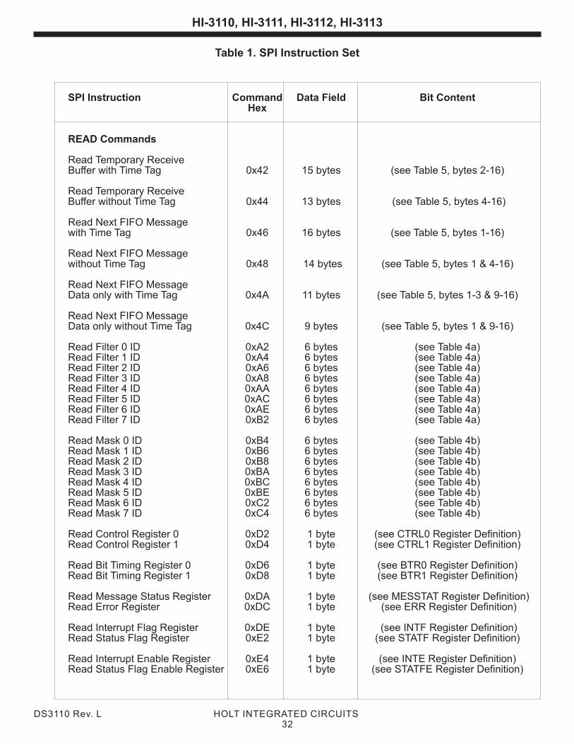
Table 1. SPI Instruction Set
SPI Instruction Command Data Field Bit ContentHex
READ Commands
Read Temporary Receive Buffer with Time Tag 0x42 15 bytes (see Table 5, bytes 2-16)
Read Temporary Receive Buffer without Time Tag 0x44 13 bytes (see Table 5, bytes 4-16)
Read Next FIFO Message with Time Tag 0x46 16 bytes (see Table 5, bytes 1-16)
Read Next FIFO Message without Time Tag 0x48 14 bytes (see Table 5, bytes 1 & 4-16)
Read Next FIFO Message Data only with Time Tag 0x4A 11 bytes (see Table 5, bytes 1-3 & 9-16)
Read Next FIFO Message Data only without Time Tag 0x4C 9 bytes (see Table 5, bytes 1 & 9-16)
Read Filter 0 ID 0xA2 6 bytes (see Table 4a)Read Filter 1 ID 0xA4 6 bytes (see Table 4a)Read Filter 2 ID 0xA6 6 bytes (see Table 4a)Read Filter 3 ID 0xA8 6 bytes (see Table 4a)Read Filter 4 ID 0xAA 6 bytes (see Table 4a)Read Filter 5 ID 0xAC 6 bytes (see Table 4a)Read Filter 6 ID 0xAE 6 bytes (see Table 4a)Read Filter 7 ID 0xB2 6 bytes (see Table 4a)
Read Mask 0 ID 0xB4 6 bytes (see Table 4b)Read Mask 1 ID 0xB6 6 bytes (see Table 4b)Read Mask 2 ID 0xB8 6 bytes (see Table 4b)Read Mask 3 ID 0xBA 6 bytes (see Table 4b)Read Mask 4 ID 0xBC 6 bytes (see Table 4b)Read Mask 5 ID 0xBE 6 bytes (see Table 4b)Read Mask 6 ID 0xC2 6 bytes (see Table 4b)Read Mask 7 ID 0xC4 6 bytes (see Table 4b)
Read Control Register 0 0xD2 1 byte (see CTRL0 Register Definition)Read Control Register 1 0xD4 1 byte (see CTRL1 Register Definition)
Read Bit Timing Register 0 0xD6 1 byte (see BTR0 Register Definition)Read Bit Timing Register 1 0xD8 1 byte (see BTR1 Register Definition)
Read Message Status Register 0xDA 1 byte (see MESSTAT Register Definition)Read Error Register 0xDC 1 byte (see ERR Register Definition)
Read Interrupt Flag Register 0xDE 1 byte (see INTF Register Definition)Read Status Flag Register 0xE2 1 byte (see STATF Register Definition)
Read Interrupt Enable Register 0xE4 1 byte (see INTE Register Definition)Read Status Flag Enable Register 0xE6 1 byte (see STATFE Register Definition)
DS3110 Rev. L HOLT INTEGRATED CIRCUITS32
HI-3110, HI-3111, HI-3112, HI-3113
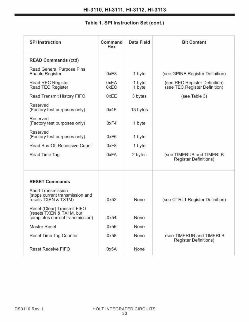
Table 1. SPI Instruction Set (cont.)
SPI Instruction Command Data Field Bit ContentHex
READ Commands (ctd)
Read General Purpose Pins Enable Register 0xE8 1 byte (see GPINE Register Definition)
Read REC Register 0xEA 1 byte (see REC Register Definition)Read TEC Register 0xEC 1 byte (see TEC Register Definition)
Read Transmit History FIFO 0xEE 3 bytes (see Table 3)
Reserved (Factory test purposes only) 0x4E 13 bytes
Reserved (Factory test purposes only) 0xF4 1 byte
Reserved (Factory test purposes only) 0xF6 1 byte
Read Bus-Off Recessive Count 0xF8 1 byte
Read Time Tag 0xFA 2 bytes (see TIMERUB and TIMERLB Register Definitions)
RESET Commands
Abort Transmission (stops current transmission andresets TXEN & TX1M) 0x52 None (see CTRL1 Register Definition)
Reset (Clear) Transmit FIFO(resets TXEN & TX1M, but completes current transmission) 0x54 None
Master Reset 0x56 None
Reset Time Tag Counter 0x58 None (see TIMERUB and TIMERLB Register Definitions)
Reset Receive FIFO 0x5A None
DS3110 Rev. L HOLT INTEGRATED CIRCUITS33
HI-3110, HI-3111, HI-3112, HI-3113
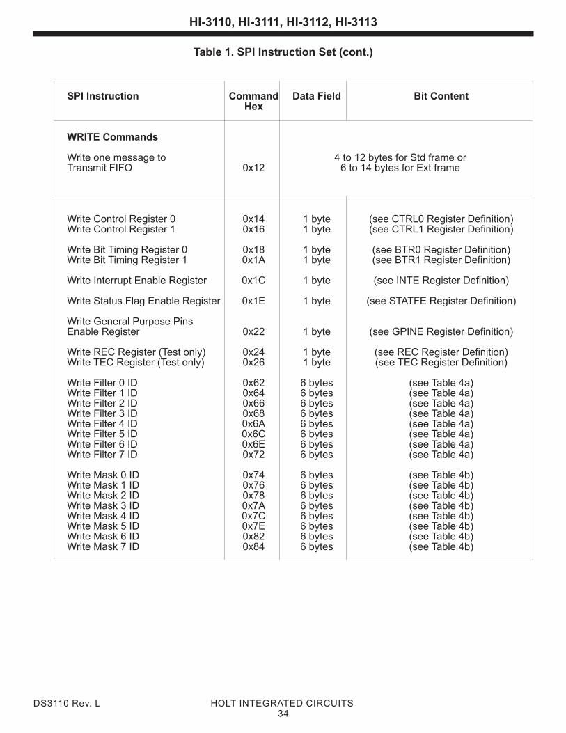
Table 1. SPI Instruction Set (cont.)
SPI Instruction Command Data Field Bit ContentHex
WRITE Commands
Write one message to 4 to 12 bytes for Std frame orTransmit FIFO 0x12 6 to 14 bytes for Ext frame
Write Control Register 0 0x14 1 byte (see CTRL0 Register Definition)Write Control Register 1 0x16 1 byte (see CTRL1 Register Definition)
Write Bit Timing Register 0 0x18 1 byte (see BTR0 Register Definition)Write Bit Timing Register 1 0x1A 1 byte (see BTR1 Register Definition)
Write Interrupt Enable Register 0x1C 1 byte (see INTE Register Definition)
Write Status Flag Enable Register 0x1E 1 byte (see STATFE Register Definition)
Write General Purpose Pins Enable Register 0x22 1 byte (see GPINE Register Definition)
Write REC Register (Test only) 0x24 1 byte (see REC Register Definition)Write TEC Register (Test only) 0x26 1 byte (see TEC Register Definition)
Write Filter 0 ID 0x62 6 bytes (see Table 4a)Write Filter 1 ID 0x64 6 bytes (see Table 4a)Write Filter 2 ID 0x66 6 bytes (see Table 4a)Write Filter 3 ID 0x68 6 bytes (see Table 4a)Write Filter 4 ID 0x6A 6 bytes (see Table 4a)Write Filter 5 ID 0x6C 6 bytes (see Table 4a)Write Filter 6 ID 0x6E 6 bytes (see Table 4a)Write Filter 7 ID 0x72 6 bytes (see Table 4a)
Write Mask 0 ID 0x74 6 bytes (see Table 4b)Write Mask 1 ID 0x76 6 bytes (see Table 4b)Write Mask 2 ID 0x78 6 bytes (see Table 4b)Write Mask 3 ID 0x7A 6 bytes (see Table 4b)Write Mask 4 ID 0x7C 6 bytes (see Table 4b)Write Mask 5 ID 0x7E 6 bytes (see Table 4b)Write Mask 6 ID 0x82 6 bytes (see Table 4b)Write Mask 7 ID 0x84 6 bytes (see Table 4b)
DS3110 Rev. L HOLT INTEGRATED CIRCUITS34
HI-3110, HI-3111, HI-3112, HI-3113
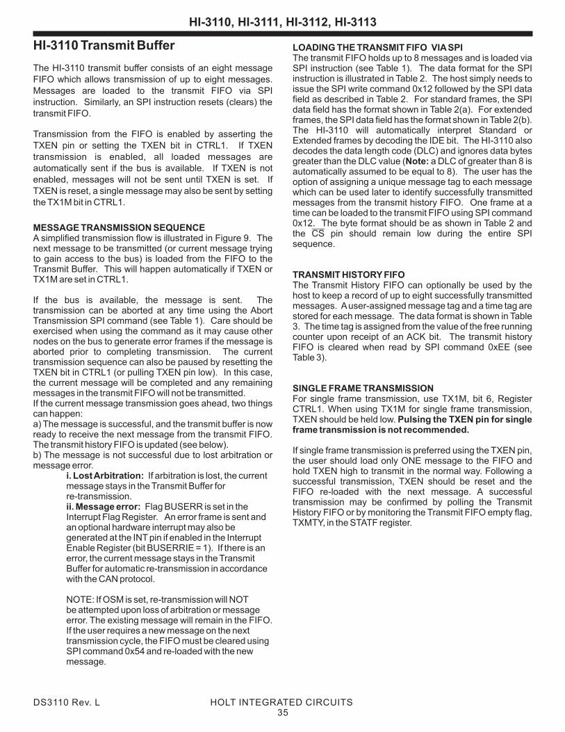
HI-3110 Transmit Buffer LOADING THE TRANSMIT FIFO VIA SPIThe transmit FIFO holds up to 8 messages and is loaded via
The HI-3110 transmit buffer consists of an eight message SPI instruction (see Table 1). The data format for the SPI instruction is illustrated in Table 2. The host simply needs to FIFO which allows transmission of up to eight messages. issue the SPI write command 0x12 followed by the SPI data Messages are loaded to the transmit FIFO via SPI field as described in Table 2. For standard frames, the SPI instruction. Similarly, an SPI instruction resets (clears) the data field has the format shown in Table 2(a). For extended transmit FIFO. frames, the SPI data field has the format shown in Table 2(b). The HI-3110 will automatically interpret Standard or Transmission from the FIFO is enabled by asserting the Extended frames by decoding the IDE bit. The HI-3110 also
TXEN pin or setting the TXEN bit in CTRL1. If TXEN decodes the data length code (DLC) and ignores data bytes
transmission is enabled, all loaded messages are greater than the DLC value (Note: a DLC of greater than 8 is automatically sent if the bus is available. If TXEN is not automatically assumed to be equal to 8). The user has the enabled, messages will not be sent until TXEN is set. If option of assigning a unique message tag to each message TXEN is reset, a single message may also be sent by setting which can be used later to identify successfully transmitted the TX1M bit in CTRL1. messages from the transmit history FIFO. One frame at a
time can be loaded to the transmit FIFO using SPI command 0x12. The byte format should be as shown in Table 2 and MESSAGE TRANSMISSION SEQUENCEthe CS pin should remain low during the entire SPI A simplified transmission flow is illustrated in Figure 9. The sequence. next message to be transmitted (or current message trying
to gain access to the bus) is loaded from the FIFO to the Transmit Buffer. This will happen automatically if TXEN or
TRANSMIT HISTORY FIFOTX1M are set in CTRL1. The Transmit History FIFO can optionally be used by the host to keep a record of up to eight successfully transmitted If the bus is available, the message is sent. The messages. A user-assigned message tag and a time tag are transmission can be aborted at any time using the Abort stored for each message. The data format is shown in Table Transmission SPI command (see Table 1). Care should be 3. The time tag is assigned from the value of the free running exercised when using the command as it may cause other counter upon receipt of an ACK bit. The transmit history nodes on the bus to generate error frames if the message is FIFO is cleared when read by SPI command 0xEE (see aborted prior to completing transmission. The current Table 3). transmission sequence can also be paused by resetting the
TXEN bit in CTRL1 (or pulling TXEN pin low). In this case, the current message will be completed and any remaining
SINGLE FRAME TRANSMISSIONmessages in the transmit FIFO will not be transmitted. For single frame transmission, use TX1M, bit 6, Register If the current message transmission goes ahead, two things CTRL1. When using TX1M for single frame transmission, can happen: TXEN should be held low. Pulsing the TXEN pin for single a) The message is successful, and the transmit buffer is now frame transmission is not recommended. ready to receive the next message from the transmit FIFO.
The transmit history FIFO is updated (see below). If single frame transmission is preferred using the TXEN pin, b) The message is not successful due to lost arbitration or the user should load only ONE message to the FIFO and message error.hold TXEN high to transmit in the normal way. Following a i. Lost Arbitration: If arbitration is lost, the current successful transmission, TXEN should be reset and the message stays in the Transmit Buffer for FIFO re-loaded with the next message. A successful re-transmission. transmission may be confirmed by polling the Transmit ii. Message error: Flag BUSERR is set in the History FIFO or by monitoring the Transmit FIFO empty flag, Interrupt Flag Register. An error frame is sent and TXMTY, in the STATF register. an optional hardware interrupt may also be
generated at the INT pin if enabled in the Interrupt Enable Register (bit BUSERRIE = 1). If there is an error, the current message stays in the Transmit Buffer for automatic re-transmission in accordance with the CAN protocol.
NOTE: If OSM is set, re-transmission will NOT be attempted upon loss of arbitration or message error. The existing message will remain in the FIFO. If the user requires a new message on the next transmission cycle, the FIFO must be cleared using SPI command 0x54 and re-loaded with the new message.
DS3110 Rev. L HOLT INTEGRATED CIRCUITS35
HI-3110, HI-3111, HI-3112, HI-3113
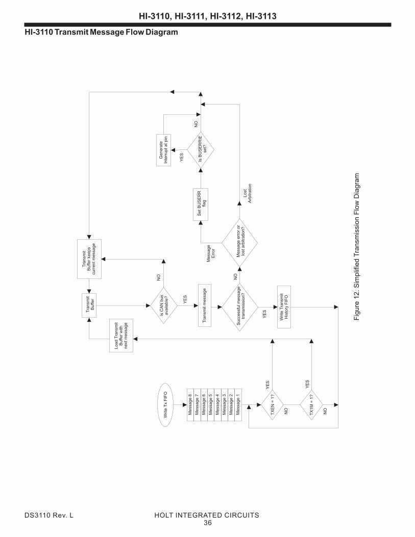
HI-3110 Transmit Message Flow Diagram
Fig
ure
12. S
implif
ied T
ransm
issi
on F
low
Dia
gra
m
DS3110 Rev. L HOLT INTEGRATED CIRCUITS36
Is C
AN
bu
s a
vaila
ble
?
YE
S
NO
Tra
nsm
it B
uffe
r
TX
1M
= 1
?
NO
Lo
ad
Tra
nsm
it B
uffe
r w
ith
ne
xt m
ess
ag
e
Tra
nsm
it B
uffe
r ke
ep
s cu
rre
nt
me
ssa
ge
Tra
nsm
it m
ess
ag
e
Su
cce
ssfu
l me
ssa
ge
tra
nsm
issi
on
?
YE
S
NO
Write
Tra
nsm
it H
isto
ry F
IFO
Me
ssa
ge
err
or
or
lost
arb
itra
tion
?L
ost
A
rbitr
atio
n
Me
ssa
ge
E
rro
r
Is B
US
ER
RIE
se
t?
YE
S
Ge
ne
rate
In
terr
up
t a
t p
in
NO
Se
t B
US
ER
R
flag
YE
S
Write
Tx
FIF
O
Me
ssa
ge
1
Me
ssa
ge
2
Me
ssa
ge
3
Me
ssa
ge
4
Me
ssa
ge
5
Me
ssa
ge
6
Me
ssa
ge
7
Me
ssa
ge
8
TX
EN
= 1
?Y
ES
NO
HI-3110, HI-3111, HI-3112, HI-3113
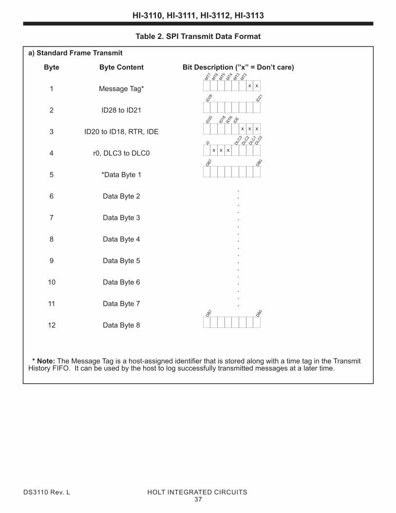
a) Standard Frame Transmit
Byte Byte Content Bit Description (”x” = Don’t care)
1 Message Tag*
2 ID28 to ID21
3 ID20 to ID18, RTR, IDE
4 r0, DLC3 to DLC0
5 *Data Byte 1
.6 Data Byte 2 .
.
.7 Data Byte 3 .
.
.8 Data Byte 4 .
.
.9 Data Byte 5 .
.
.10 Data Byte 6 .
.
.11 Data Byte 7 .
12 Data Byte 8
* Note: The Message Tag is a host-assigned identifier that is stored along with a time tag in the Transmit History FIFO. It can be used by the host to log successfully transmitted messages at a later time.
ID28
ID21
MT2
x x
MT7
MT3
MT5
MT6
MT4
DB7
DB0
DB7
DB0
ID20
ID18
x x
RTR
IDE
x
Table 2. SPI Transmit Data Format
r0 DLC
0
x xx
DLC
3D
LC2
DLC
1
DS3110 Rev. L HOLT INTEGRATED CIRCUITS37
HI-3110, HI-3111, HI-3112, HI-3113
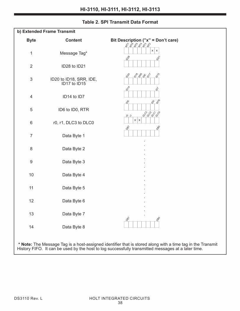
b) Extended Frame Transmit
Byte Content Bit Description (”x” = Don’t care)
1 Message Tag*
2 ID28 to ID21
3 ID20 to ID18, SRR, IDE,ID17 to ID15
4 ID14 to ID7
5 ID6 to ID0, RTR
6 r0, r1, DLC3 to DLC0
7 Data Byte 1..
8 Data Byte 2 ...
9 Data Byte 3 ...
10 Data Byte 4 ...
11 Data Byte 5 ...
12 Data Byte 6 ...
13 Data Byte 7 .
14 Data Byte 8
* Note: The Message Tag is a host-assigned identifier that is stored along with a time tag in the Transmit History FIFO. It can be used by the host to log successfully transmitted messages at a later time.
ID28
ID21
MT2
x x
MT7
MT3
MT5
MT6
MT4
DB7
DB0
DB7
DB0
ID6
RTR
ID0
ID14
ID7
ID20
ID18
SR
RID
E
ID17
ID15
Table 2. SPI Transmit Data Format
r0 DLC
0
x x
DLC
3D
LC2
DLC
1
r1
DS3110 Rev. L HOLT INTEGRATED CIRCUITS38
HI-3110, HI-3111, HI-3112, HI-3113
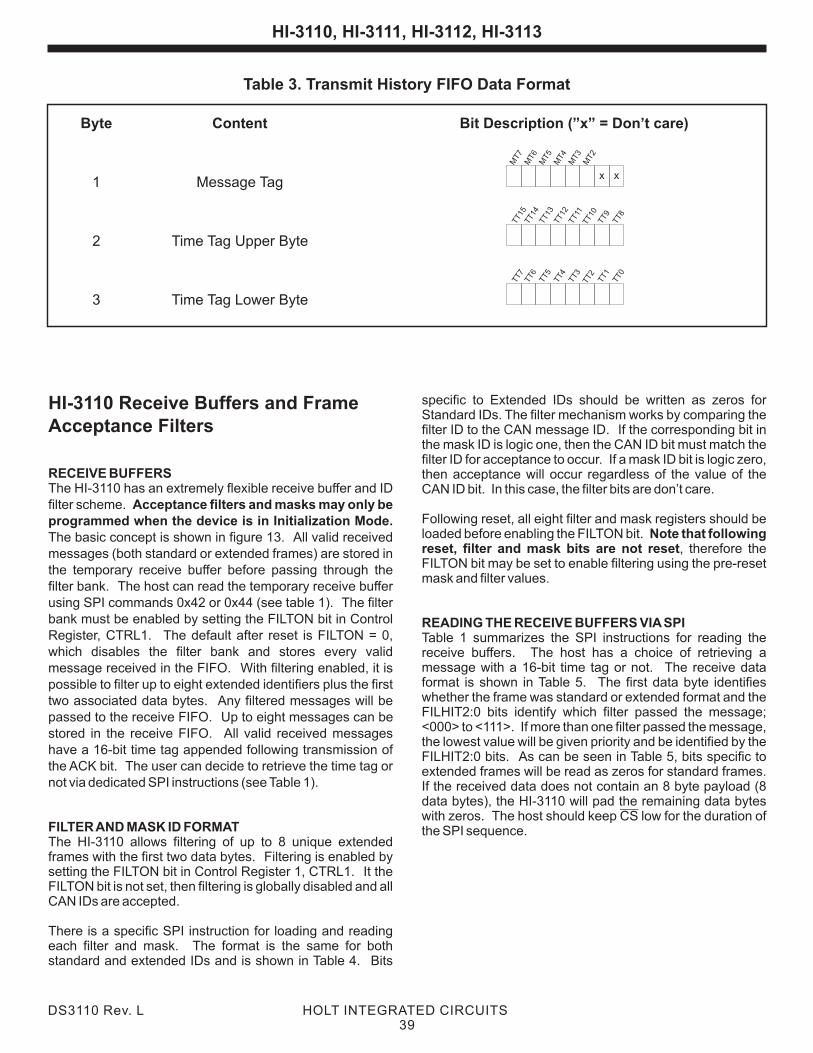
specific to Extended IDs should be written as zeros for HI-3110 Receive Buffers and Frame Standard IDs. The filter mechanism works by comparing the
Acceptance Filters filter ID to the CAN message ID. If the corresponding bit in the mask ID is logic one, then the CAN ID bit must match the filter ID for acceptance to occur. If a mask ID bit is logic zero,
RECEIVE BUFFERS then acceptance will occur regardless of the value of the The HI-3110 has an extremely flexible receive buffer and ID CAN ID bit. In this case, the filter bits are don’t care. filter scheme. Acceptance filters and masks may only be
Following reset, all eight filter and mask registers should be programmed when the device is in Initialization Mode. loaded before enabling the FILTON bit. Note that following The basic concept is shown in figure 13. All valid received reset, filter and mask bits are not reset, therefore the messages (both standard or extended frames) are stored in FILTON bit may be set to enable filtering using the pre-reset the temporary receive buffer before passing through the mask and filter values.
filter bank. The host can read the temporary receive buffer using SPI commands 0x42 or 0x44 (see table 1). The filter bank must be enabled by setting the FILTON bit in Control READING THE RECEIVE BUFFERS VIA SPIRegister, CTRL1. The default after reset is FILTON = 0, Table 1 summarizes the SPI instructions for reading the which disables the filter bank and stores every valid receive buffers. The host has a choice of retrieving a
message with a 16-bit time tag or not. The receive data message received in the FIFO. With filtering enabled, it is format is shown in Table 5. The first data byte identifies possible to filter up to eight extended identifiers plus the first whether the frame was standard or extended format and the two associated data bytes. Any filtered messages will be FILHIT2:0 bits identify which filter passed the message; passed to the receive FIFO. Up to eight messages can be <000> to <111>. If more than one filter passed the message, stored in the receive FIFO. All valid received messages the lowest value will be given priority and be identified by the
have a 16-bit time tag appended following transmission of FILHIT2:0 bits. As can be seen in Table 5, bits specific to
the ACK bit. The user can decide to retrieve the time tag or extended frames will be read as zeros for standard frames. not via dedicated SPI instructions (see Table 1). If the received data does not contain an 8 byte payload (8 data bytes), the HI-3110 will pad the remaining data bytes
with zeros. The host should keep CS low for the duration of FILTER AND MASK ID FORMAT the SPI sequence.The HI-3110 allows filtering of up to 8 unique extended frames with the first two data bytes. Filtering is enabled by setting the FILTON bit in Control Register 1, CTRL1. It the FILTON bit is not set, then filtering is globally disabled and all CAN IDs are accepted.
There is a specific SPI instruction for loading and reading each filter and mask. The format is the same for both standard and extended IDs and is shown in Table 4. Bits
Table 3. Transmit History FIFO Data Format
Byte Content Bit Description (”x” = Don’t care)
1 Message Tag
2 Time Tag Upper Byte
3 Time Tag Lower Byte
TT15
TT8
TT14
TT13
TT12
TT11
TT10
TT9
TT7
TT0
TT6
TT5
TT4
TT3
TT2
TT1
MT2
x x
MT7
MT3
MT5
MT6
MT4
DS3110 Rev. L HOLT INTEGRATED CIRCUITS39
HI-3110, HI-3111, HI-3112, HI-3113
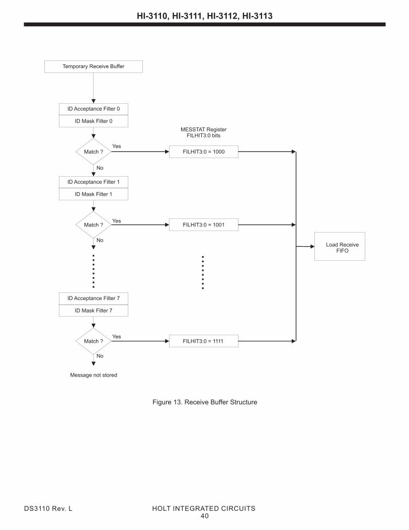
Load Receive FIFO
Match ?
Match ?
Match ?
MESSTAT Register FILHIT3:0 bits
FILHIT3:0 = 1000
FILHIT3:0 = 1001
FILHIT3:0 = 1111
........
Yes
No
Yes
Yes
No
No
Message not stored
Temporary Receive Buffer
ID Acceptance Filter 0
ID Mask Filter 0
ID Acceptance Filter 1
ID Mask Filter 1
ID Acceptance Filter 7
ID Mask Filter 7
........
Figure 13. Receive Buffer Structure
DS3110 Rev. L HOLT INTEGRATED CIRCUITS40
HI-3110, HI-3111, HI-3112, HI-3113
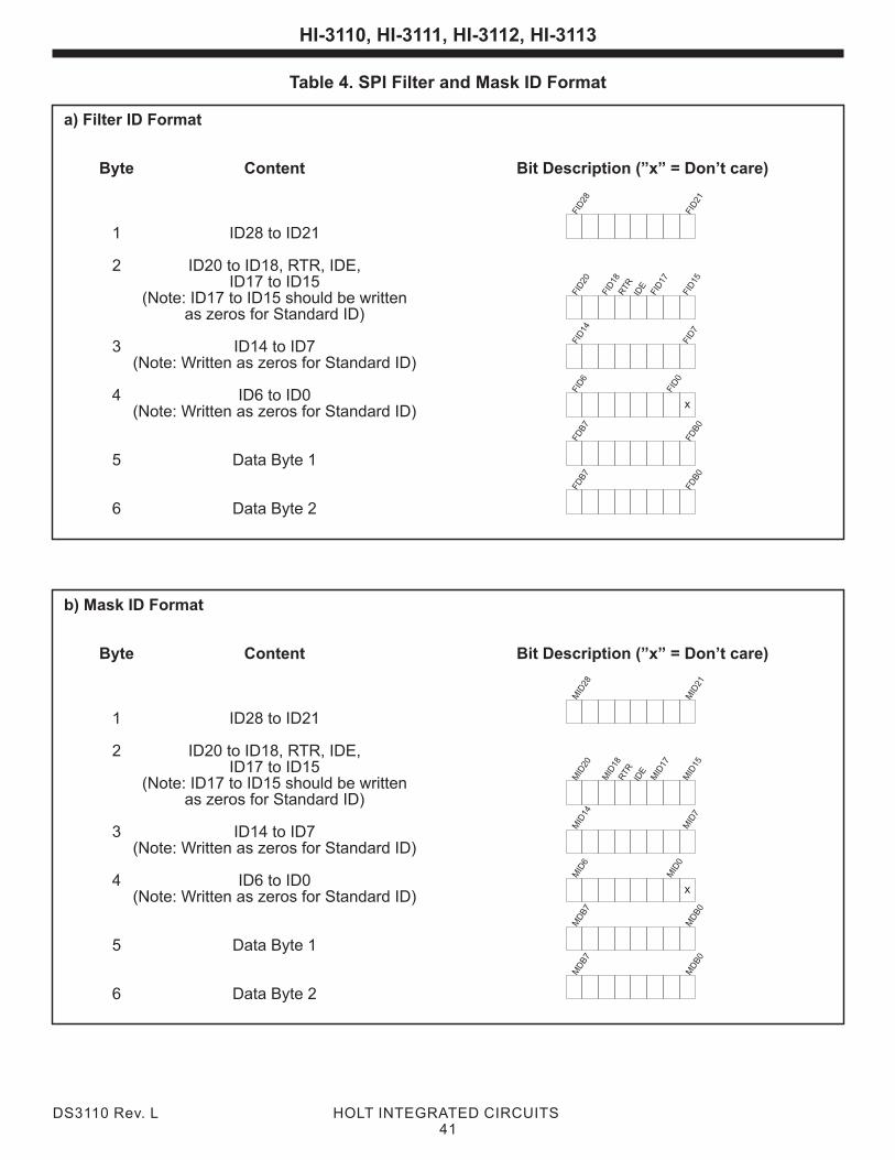
b) Mask ID Format
Byte Content Bit Description (”x” = Don’t care)
1 ID28 to ID21
2 ID20 to ID18, RTR, IDE,ID17 to ID15
(Note: ID17 to ID15 should be written as zeros for Standard ID)
3 ID14 to ID7 (Note: Written as zeros for Standard ID)
4 ID6 to ID0 (Note: Written as zeros for Standard ID)
5 Data Byte 1
6 Data Byte 2
MD
B7
MD
B0
MD
B7
MD
B0
MID
14
MID
7
MID
28
MID
21
RTR
MID
20
MID
18
MID
17
MID
15
IDE
MID
6
MID
0
x
a) Filter ID Format
Byte Content Bit Description (”x” = Don’t care)
1 ID28 to ID21
2 ID20 to ID18, RTR, IDE,ID17 to ID15
(Note: ID17 to ID15 should be written as zeros for Standard ID)
3 ID14 to ID7 (Note: Written as zeros for Standard ID)
4 ID6 to ID0 (Note: Written as zeros for Standard ID)
5 Data Byte 1
6 Data Byte 2
Table 4. SPI Filter and Mask ID Format
FD
B7
FD
B0
FD
B7
FD
B0
FID
14
FID
7
FID
28
FID
21
RTR
FID
20
FID
18
FID
17
FID
15
IDE
FID
6
FID
0
x
DS3110 Rev. L HOLT INTEGRATED CIRCUITS41
HI-3110, HI-3111, HI-3112, HI-3113
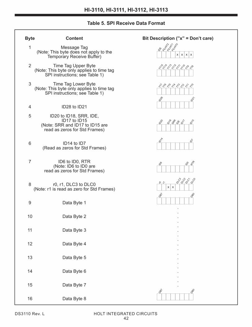
Byte Content Bit Description (”x” = Don’t care)
1 Message Tag (Note: This byte does not apply to the
Temporary Receive Buffer)
2 Time Tag Upper Byte (Note: This byte only applies to time tag
SPI instructions; see Table 1)
3 Time Tag Lower Byte (Note: This byte only applies to time tag
SPI instructions; see Table 1)
4 ID28 to ID21
5 ID20 to ID18, SRR, IDE,ID17 to ID15
(Note: SRR and ID17 to ID15 are read as zeros for Std Frames)
6 ID14 to ID7 (Read as zeros for Std Frames)
7 ID6 to ID0, RTR(Note: ID6 to ID0 are
read as zeros for Std Frames)
8 r0, r1, DLC3 to DLC0(Note: r1 is read as zero for Std Frames)
9 Data Byte 1..
10 Data Byte 2 ...
11 Data Byte 3 ...
12 Data Byte 4 ...
13 Data Byte 5 ...
14 Data Byte 6 ...
15 Data Byte 7 .
16 Data Byte 8
DB7
DB0
DB7
DB0
r0 DLC
0
x x
DLC
3D
LC2
DLC
1
r1
ID6
RTR
ID0
ID14
ID7
ID20
ID18
SR
RID
E
ID17
ID15
x x
IDE
FIL
HIT
1
FIL
HIT
2
FIL
HIT
0
xx
TT15
TT8
TT14
TT13
TT12
TT11
TT10
TT9
TT7
TT0
TT6
TT5
TT4
TT3
TT2
TT1
ID28
ID21
Table 5. SPI Receive Data Format
DS3110 Rev. L HOLT INTEGRATED CIRCUITS42
HI-3110, HI-3111, HI-3112, HI-3113
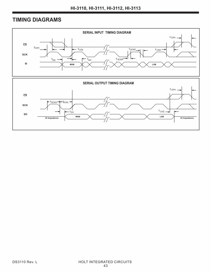
SERIAL INPUT TIMING DIAGRAM
CS
SCK
SI
CHHtCSHt
MSB
CSSt
DSt t
DH
LSB
CPHt
SCKRt
SCKFt
TIMING DIAGRAMS
SERIAL OUTPUT TIMING DIAGRAM
CS
SCK
SOCHZt
Hi Impedance
SCKHt
t DV
LSB
CPHt
tSCKL
MSBHi Impedance
DS3110 Rev. L HOLT INTEGRATED CIRCUITS43
HI-3110, HI-3111, HI-3112, HI-3113
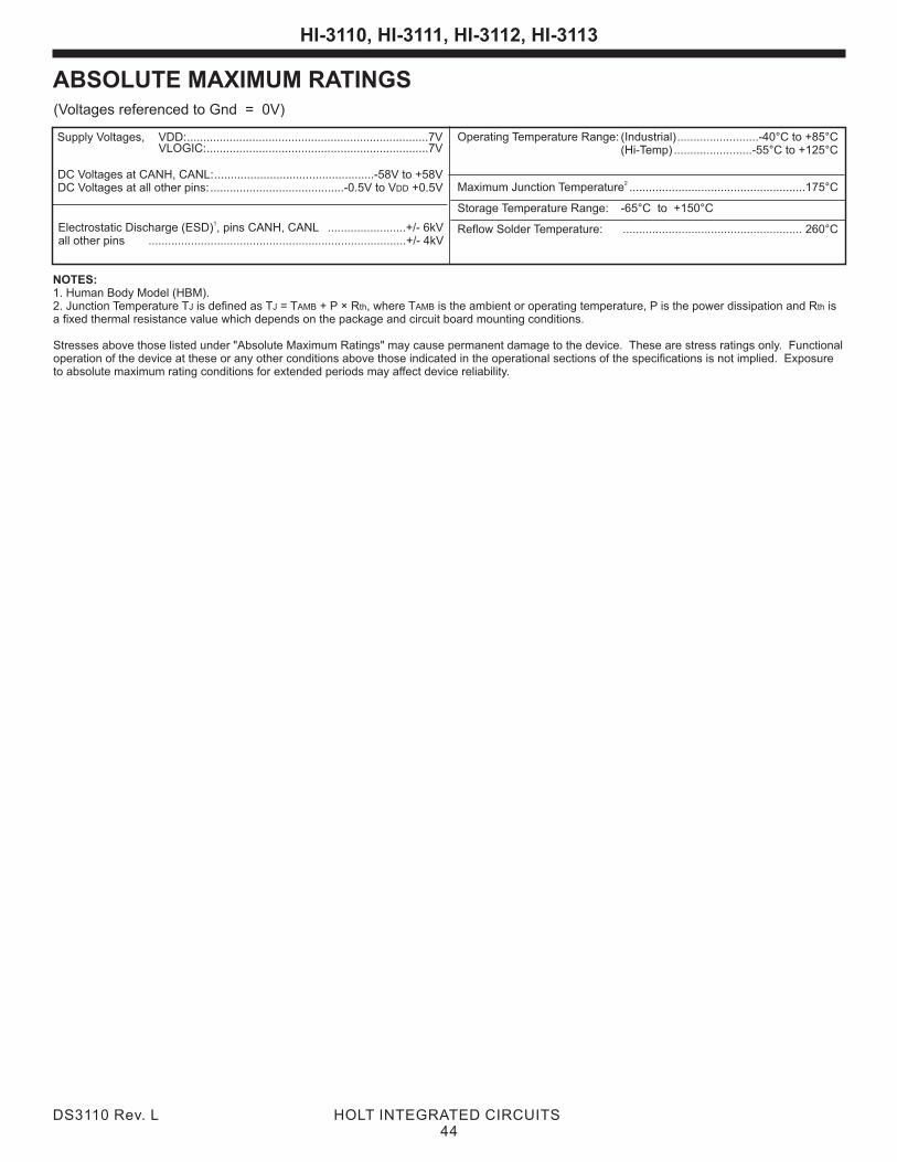
NOTES:1. Human Body Model (HBM).2. Junction Temperature T is defined as T = T + P × R , where T is the ambient or operating temperature, P is the power dissipation and R is a fixed thermal resistance value which depends on the package and circuit board mounting conditions.
Stresses above those listed under "Absolute Maximum Ratings" may cause permanent damage to the device. These are stress ratings only. Functional operation of the device at these or any other conditions above those indicated in the operational sections of the specifications is not implied. Exposure to absolute maximum rating conditions for extended periods may affect device reliability.
J J AMB th AMB th
ABSOLUTE MAXIMUM RATINGS
(Hi-Temp) ........................-55°C to +125°C
Maximum Junction Temperature
Storage Temperature Range: -65°C to +150°C
Reflow Solder Temperature:
Operating Temperature Range: (Industrial).........................-40°C to +85°C
2 ......................................................175°C
....................................................... 260°C
Supply Voltages, VDD:..........................................................................7V VLOGIC:....................................................................7V
:.................................................
Electrostatic Discharge (ESD) , pins CANH, CANL ........................+/- 6kVall other pins ...............................................................................+/- 4kV
DC Voltages at CANH, CANL -58V to +58VDC Voltages at all other pins:.........................................-0.5V to V +0.5V
1
DD
(Voltages referenced to Gnd = 0V)
DS3110 Rev. L HOLT INTEGRATED CIRCUITS44
HI-3110, HI-3111, HI-3112, HI-3113
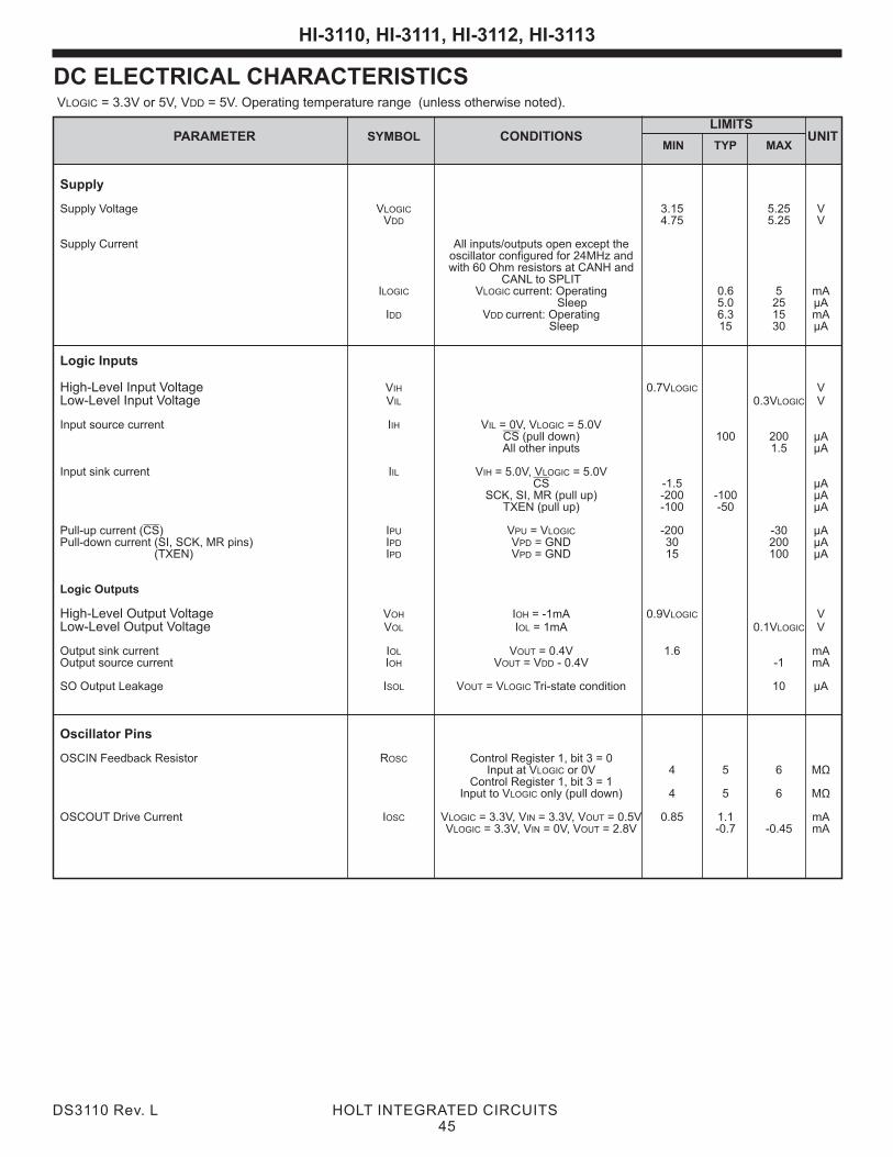
DC ELECTRICAL CHARACTERISTICS V = 3.3V or 5V, V = Operating temperature range (unless otherwise noted). LOGIC DD 5V.
LIMITS PARAMETER CONDITIONS UNITSYMBOL
MIN TYP MAX
Supply Voltage VLOGIC 3.15 5.25 VVDD 4.75 5.25 V
Supply Current All inputs/outputs open except the oscillator configured for 24MHz and with 60 Ohm resistors at CANH and
CANL to SPLITILOGIC VLOGIC current: Operating 0.6 5 mA
Sleep 5.0 25 µAIDD VDD current: Operating 6.3 15 mA
Sleep 15 30 µA
Logic Inputs
High-Level Input Voltage VIH 0.7VLOGIC VLow-Level Input Voltage VIL 0.3VLOGIC V
Input source current IIH VIL = 0V, VLOGIC = 5.0VCS (pull down) 100 200 µAAll other inputs 1.5 µA
Input sink current IIL VIH = 5.0V, VLOGIC = 5.0VCS -1.5 µA
SCK, SI, MR (pull up) -200 -100 µATXEN (pull up) -100 -50 µA
Pull-up current (CS) IPU VPU = VLOGIC -200 -30 µAPull-down current (SI, SCK, MR pins) IPD VPD = GND 30 200 µA (TXEN) IPD VPD = GND 15 100 µA
Logic Outputs
High-Level Output Voltage VOH IOH = -1mA 0.9VLOGIC VLow-Level Output Voltage VOL IOL = 1mA 0.1VLOGIC V
Output sink current IOL VOUT = 0.4V 1.6 mAOutput source current IOH VOUT = VDD - 0.4V -1 mA
SO Output Leakage ISOL VOUT = VLOGIC Tri-state condition 10 µA
Oscillator Pins
OSCIN Feedback Resistor ROSC Control Register 1, bit 3 = 0Input at VLOGIC or 0V 4 5 6 MΩ
Control Register 1, bit 3 = 1Input to VLOGIC only (pull down) 4 5 6 MΩ
OSCOUT Drive Current IOSC VLOGIC = 3.3V, VIN = 3.3V, VOUT = 0.5V 0.85 1.1 mAVLOGIC = 3.3V, VIN = 0V, VOUT = 2.8V -0.7 -0.45 mA
Supply
DS3110 Rev. L HOLT INTEGRATED CIRCUITS45
HI-3110, HI-3111, HI-3112, HI-3113
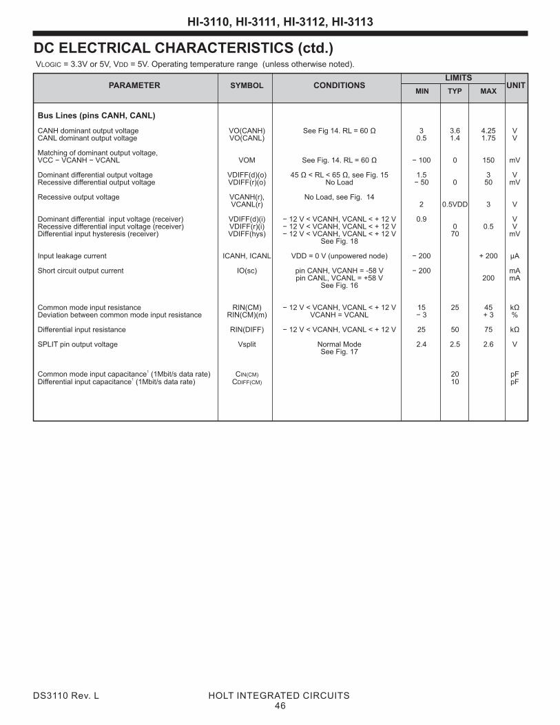
DC ELECTRICAL CHARACTERISTICS (ctd.) V = 3.3V or 5V, V = Operating temperature range (unless otherwise noted). LOGIC DD 5V.
LIMITS PARAMETER CONDITIONS UNITSYMBOL
MIN TYP MAX
CANH dominant output voltage VO(CANH) See Fig 14. RL = 60 Ω 3 3.6 4.25 VCANL dominant output voltage VO(CANL) 0.5 1.4 1.75 V
Matching of dominant output voltage,VCC − VCANH − VCANL VOM See Fig. 14. RL = 60 Ω − 100 0 150 mV
Dominant differential output voltage VDIFF(d)(o) 45 Ω < RL < 65 Ω, see Fig. 15 1.5 3 VRecessive differential output voltage VDIFF(r)(o) No Load − 50 0 50 mV
Recessive output voltage VCANH(r), No Load, see Fig. 14VCANL(r) 2 0.5VDD 3 V
Dominant differential input voltage (receiver) VDIFF(d)(i) − 12 V < VCANH, VCANL < + 12 V 0.9 VRecessive differential input voltage (receiver) VDIFF(r)(i) − 12 V < VCANH, VCANL < + 12 V 0 0.5 VDifferential input hysteresis (receiver) VDIFF(hys) − 12 V < VCANH, VCANL < + 12 V 70 mV
See Fig. 18
Input leakage current ICANH, ICANL VDD = 0 V (unpowered node) − 200 + 200 µA
Short circuit output current IO(sc) pin CANH, VCANH = -58 V − 200 mApin CANL, VCANL = +58 V 200 mA
See Fig. 16
Common mode input resistance RIN(CM) − 12 V < VCANH, VCANL < + 12 V 15 25 45 kΩDeviation between common mode input resistance RIN(CM)(m) VCANH = VCANL − 3 + 3 %
Differential input resistance RIN(DIFF) − 12 V < VCANH, VCANL < + 12 V 25 50 75 kΩ
SPLIT pin output voltage Vsplit Normal Mode 2.4 2.5 2.6 VSee Fig. 17
1Common mode input capacitance (1Mbit/s data rate) CIN(CM) 20 pF 1 Differential input capacitance (1Mbit/s data rate) CDIFF(CM) 10 pF
Bus Lines (pins CANH, CANL)
DS3110 Rev. L HOLT INTEGRATED CIRCUITS46
HI-3110, HI-3111, HI-3112, HI-3113
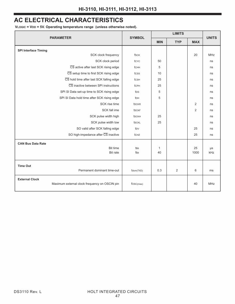
AC ELECTRICAL CHARACTERISTICS
LIMITSPARAMETER SYMBOL UNITS
MIN TYP MAX
SPI Interface Timing
SCK clock frequency fSCK
SCK clock period tCYC 50 ns
CS active after last SCK rising edge tCHH 5 ns
CS setup time to first SCK rising edge tCSS 10 ns
CS hold time after last SCK falling edge tCSH 25 ns
CS inactive between SPI instructions tCPH 25 ns
SPI SI Data set-up time to SCK rising edge t 5 ns
SPI SI Data hold time after SCK rising edge tDH 5 ns
SCK rise time tSCKR 2 ns
SCK fall ime tSCKF 2 ns
SCK pulse width high tSCKH 25 ns
SCK pulse width low tSCKL 25 ns
SO valid after SCK falling edge tDV 25 ns
SO high-impedance after CS inactive tCHZ 25 ns
CAN Bus Data Rate
Bit time tBit 1 25 µs
Bit rate fBit 40 1000 kHz
Time Out
Permanent dominant time-out tdom(TXD) 0.3 2 6 ms
External Clock
Maximum external clock frequency on OSCIN pin fOSC(max) 40 MHz
20 MHz
DS
V = V = Operating temperature range (unless otherwise noted). LOGIC DD 5V.
DS3110 Rev. L HOLT INTEGRATED CIRCUITS47
HI-3110, HI-3111, HI-3112, HI-3113
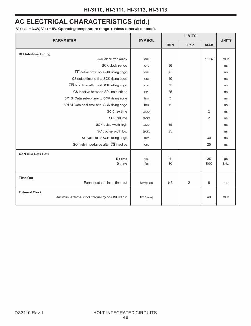
AC ELECTRICAL CHARACTERISTICS (ctd.)
LIMITSPARAMETER SYMBOL UNITS
MIN TYP MAX
SPI Interface Timing
SCK clock frequency fSCK
SCK clock period tCYC 66 ns
CS active after last SCK rising edge tCHH 5 ns
CS setup time to first SCK rising edge tCSS 10 ns
CS hold time after last SCK falling edge tCSH 25 ns
CS inactive between SPI instructions tCPH 25 ns
SPI SI Data set-up time to SCK rising edge t 5 ns
SPI SI Data hold time after SCK rising edge tDH 5 ns
SCK rise time tSCKR 2 ns
SCK fall ime tSCKF 2 ns
SCK pulse width high tSCKH 25 ns
SCK pulse width low tSCKL 25 ns
SO valid after SCK falling edge tDV 30 ns
SO high-impedance after CS inactive tCHZ 25 ns
CAN Bus Data Rate
Bit time tBit 1 25 µs
Bit rate fBit 40 1000 kHz
Time Out
Permanent dominant time-out tdom(TXD) 0.3 2 6 ms
External Clock
Maximum external clock frequency on OSCIN pin fOSC(max) 40 MHz
16.66 MHz
DS
VLOGIC = 3.3V, VDD = 5V. Operating temperature range (unless otherwise noted).
DS3110 Rev. L HOLT INTEGRATED CIRCUITS48
HI-3110, HI-3111, HI-3112, HI-3113
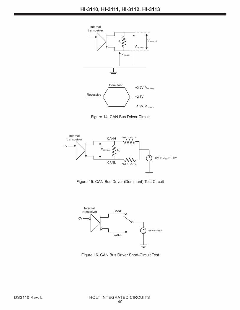
Figure 15. CAN Bus Driver (Dominant) Test Circuit
Figure 16. CAN Bus Driver Short-Circuit Test
Figure 14. CAN Bus Driver Circuit
Recessive
Dominant
~2.5V
~3.5V: VO(CANH)
~1.5V: VO(CANL)
VO(CANH)
VO(CANL)
Internal transceiver
RLVDIFF(d)(o)
CANH 300 +/- 1%W
300 +/- 1%W CANL
+_
VDIFF(d)(o)
0V
Internal transceiver
RL
-12V <= V <= +12VTEST
0V
Internal transceiver
-58V or +58V
CANH
CANL
+_
DS3110 Rev. L HOLT INTEGRATED CIRCUITS49
HI-3110, HI-3111, HI-3112, HI-3113
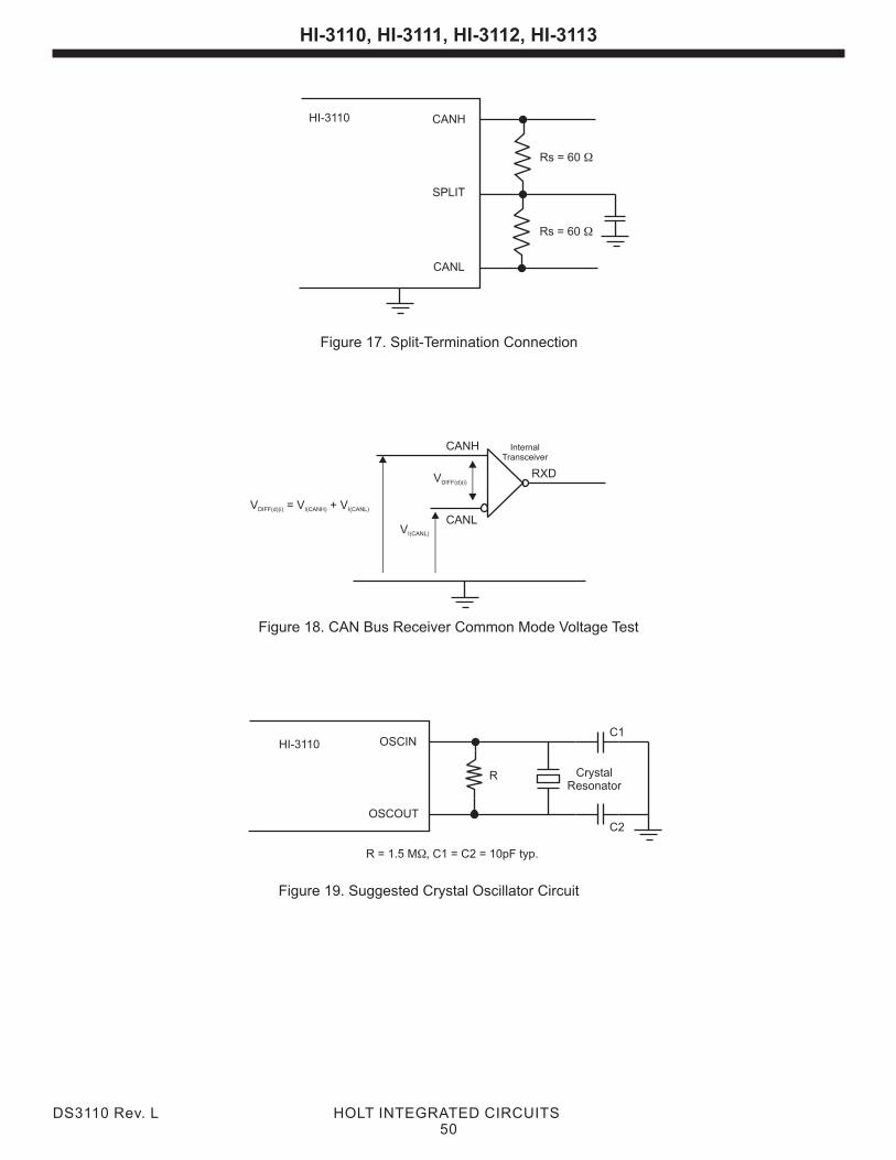
Figure 17. Split-Termination Connection
Figure 18. CAN Bus Receiver Common Mode Voltage Test
VI(CANL)
VDIFF(d)(i)
CANH
CANL
RXD
V = VDIFF(d)(i) I(CANL)V + I(CANH)
HI-3110 CANH
CANL
SPLIT
Rs = 60 W
Rs = 60 W
Internal Transceiver
Figure 19. Suggested Crystal Oscillator Circuit
HI-3110 OSCIN
OSCOUT
R
R = 1.5 M C1 = C2 = 10pF typ. W,
Crystal Resonator
C1
C2
DS3110 Rev. L HOLT INTEGRATED CIRCUITS50
HI-3110, HI-3111, HI-3112, HI-3113
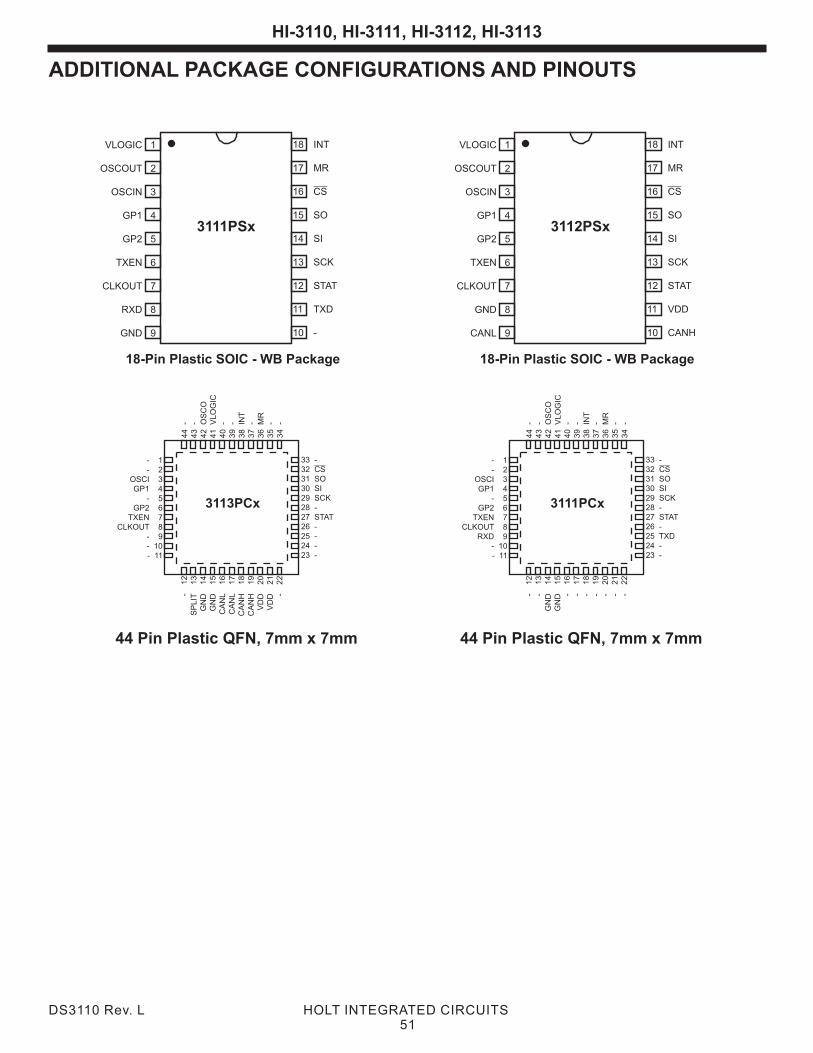
ADDITIONAL PACKAGE CONFIGURATIONS AND PINOUTS
- S
PLIT
13
GN
D 14
GN
D 15
C
AN
L 16
CA
NL 17
CA
NH
18
CA
NH
19
VD
D 20
VD
D 21
- 2
2
1
244 -
43 -
42 O
SC
O41 V
LO
GIC
40 -
39 -
38 IN
T37 -
36 M
R35 -
34 -
- 1- 2
OSCI 3GP1 4
- 5GP2 6
TXEN 7 CLKOUT 8
- 9- 10- 11
33 -32 CS31 SO30 SI29 SCK28 -27 STAT26 -25 -24 -23 -
3113PCx
44 Pin Plastic QFN, 7mm x 7mm
3111PSx
VLOGIC 1
OSCOUT 2
OSCIN 3
GP1 4
GP2 5
TXEN 6
CLKOUT 7
RXD 8
GND 9
18 INT
17 MR
16 CS
15 SO
14 SI
13 SCK
12 STAT
11 TXD
10 -
3112PSx
VLOGIC 1
OSCOUT 2
OSCIN 3
GP1 4
GP2 5
TXEN 6
CLKOUT 7
GND 8
CANL 9
18 INT
17 MR
16 CS
15 SO
14 SI
13 SCK
12 STAT
11 VDD
10 CANH
18-Pin Plastic SOIC - WB Package18-Pin Plastic SOIC - WB Package
DS3110 Rev. L HOLT INTEGRATED CIRCUITS51
- - 1
3G
ND
14
GN
D 15
-
1
6-
1
7-
1
8-
1
9-
2
0-
2
1-
2
2
1
244 -
43 -
42 O
SC
O41 V
LO
GIC
40 -
39 -
38 IN
T37 -
36 M
R35 -
34 -
- 1- 2
OSCI 3GP1 4
- 5GP2 6
TXEN 7 CLKOUT 8
RXD 9- 10- 11
33 -32 CS31 SO30 SI29 SCK28 -27 STAT26 -25 TXD24 -23 -
3111PCx
44 Pin Plastic QFN, 7mm x 7mm
HI-3110, HI-3111, HI-3112, HI-3113
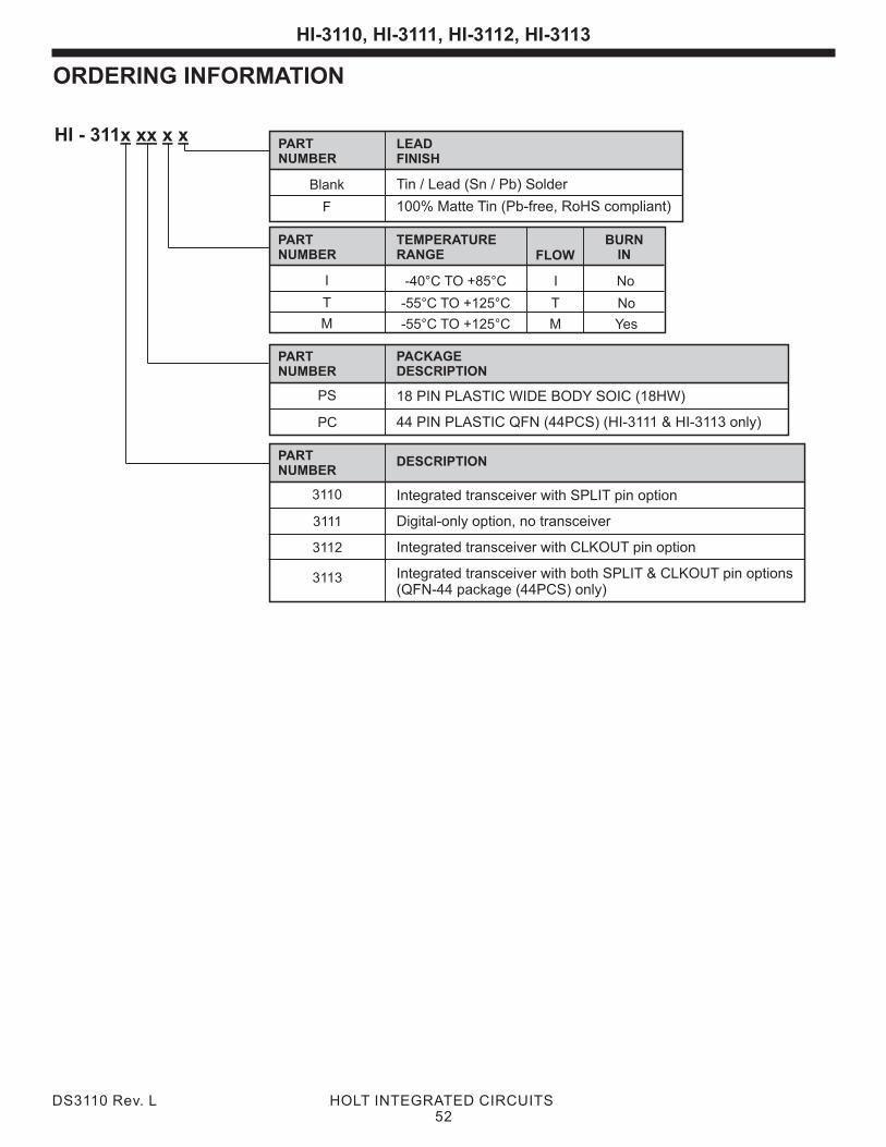
ORDERING INFORMATION
HI - 311x xx x x
PACKAGEDESCRIPTION
18 PIN PLASTIC WIDE BODY SOIC (18HW)
PARTNUMBER
PS
44 PIN PLASTIC QFN (44PCS) (HI-3111 & HI-3113 only)PC
LEADFINISH
PARTNUMBER
100% Matte Tin (Pb-free, RoHS compliant)F
Tin / Lead (Sn / Pb) SolderBlank
DESCRIPTION
Integrated transceiver with SPLIT pin option
PARTNUMBER
3110
Digital-only option, no transceiver3111
Integrated transceiver with CLKOUT pin option3112
Integrated transceiver with both SPLIT & CLKOUT pin options (QFN-44 package (44PCS) only)
3113
TEMPERATURERANGE
BURNIN
-40°C TO +85°C No
-55°C TO +125°C NoT
PARTNUMBER
T
I
FLOW
I
-55°C TO +125°C YesMM
DS3110 Rev. L HOLT INTEGRATED CIRCUITS52
HI-3110, HI-3111, HI-3112, HI-3113
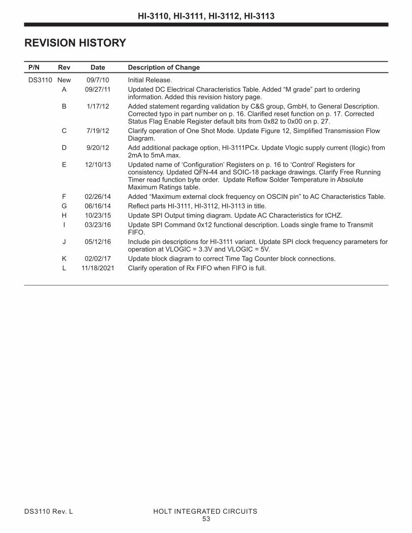
REVISION HISTORY
P/N Rev Date Description of Change
A 09/27/11 Updated DC Electrical Characteristics Table. Added “M grade” part to ordering information. Added this revision history page.
B 1/17/12 Added statement regarding validation by C&S group, GmbH, to General Description. Corrected typo in part number on p. 16. Clarified reset function on p. 17. Corrected Status Flag Enable Register default bits from 0x82 to 0x00 on p. 27.
C 7/19/12 Clarify operation of One Shot Mode. Update Figure 12, Simplified Transmission Flow Diagram.
D 9/20/12 Add additional package option, HI-3111PCx. Update Vlogic supply current (Ilogic) from 2mA to 5mA max.
E 12/10/13 Updated name of ‘Configuration’ Registers on p. 16 to ‘Control’ Registers for consistency. Updated QFN-44 and SOIC-18 package drawings. Clarify Free Running Timer read function byte order. Update Reflow Solder Temperature in Absolute Maximum Ratings table.
F 02/26/14 Added “Maximum external clock frequency on OSCIN pin” to AC Characteristics Table.
G 06/16/14 Reflect parts HI-3111, HI-3112, HI-3113 in title.
H 10/23/15 Update SPI Output timing diagram. Update AC Characteristics for tCHZ.
I 03/23/16 Update SPI Command 0x12 functional description. Loads single frame to Transmit FIFO.
J 05/12/16 Include pin descriptions for HI-3111 variant. Update SPI clock frequency parameters for operation at VLOGIC = 3.3V and VLOGIC = 5V.
K 02/02/17 Update block diagram to correct Time Tag Counter block connections.
L 11/18/2021 Clarify operation of Rx FIFO when FIFO is full.
DS3110 New 09/7/10 Initial Release.
DS3110 Rev. L HOLT INTEGRATED CIRCUITS53
HI-3110, HI-3111, HI-3112, HI-3113
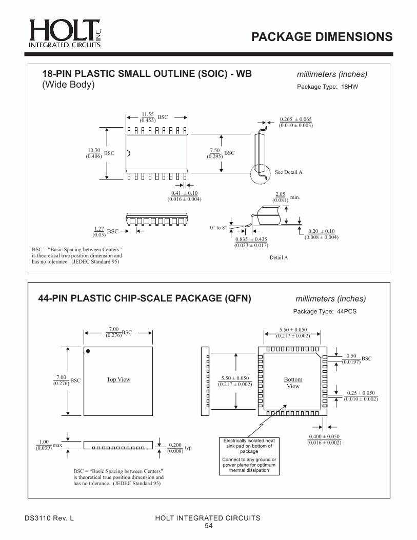
PACKAGE DIMENSIONS
DS3110 Rev. L HOLT INTEGRATED CIRCUITS54
44-PIN PLASTIC CHIP-SCALE PACKAGE (QFN)
Package Type: 44PCS
BSC = “Basic Spacing between Centers” is theoretical true position dimension and has no tolerance. (JEDEC Standard 95)
5.50 ± 0.050(0.217 ± 0.002)
0.400 ± 0.050(0.016 ± 0.002)
0.25 (0.010 )
± 0.050± 0.002
0.50(0.0197)
0.200 (0.008)
1.00(0.039)
7.00(0.276)
BSC
5.50 ± 0.050(0.217 ± 0.002)
typ
BottomView
Top ViewBSC
7.00(0.276)
BSC
max
millimeters (inches)
Electrically isolated heat sink pad on bottom of
package
Connect to any ground or power plane for optimum
thermal dissipation
18-PIN PLASTIC SMALL OUTLINE (SOIC) - WB(Wide Body)
millimeters (inches)
Package Type: 18HW
BSC = “Basic Spacing between Centers” is theoretical true position dimension and has no tolerance. (JEDEC Standard 95)
11.55(0.455)
10.30(0.406)
7.50(0.295)
0° to 8°
0.835 ± 0.435(0.033 ± 0.017)
2.05(0.081)
0.20 ± 0.10(0.008 ± 0.004)
0.265 ± 0.065(0.010 ± 0.003)
1.27(0.05)
BSC
See Detail A
Detail A
0.41 ± 0.10(0.016 ± 0.004)
BSC
BSC BSC
min.