Embed Size (px)
Citation preview
NASA TECHNICAL NOTE
0 o* - P n z + 4 m 4 z
h NASA TN D-4190
z E
HETERODYNE OPERATION OF AVALANCHE PHOTODIODES
by D, E. Sawyer
E Zectronics Research Center
Cambridge, Mass. I l 1 I 1
i / NATIONAL AERONAUTICS A N D SPACE A D M I N I S T R A T I O N W A S H I N G T O N , D. C. OCTOBER 1967
i I
-
TECH LIBRARY KAFB, NM
I Illill 11111 1111 lllll11111 lllll lllll Ill1 1111 OL308bL
NASA T N D-4190
HETERODYNE OPERATIONOF AVALANCHE PHOTODIODES
By D. E. Sawyer
Electronics Research Center Cambridge, Mass.
NATIONAL AERONAUTICS AND SPACE ADMINISTRATION
For sale by the Clearinghouse for Federal Scientific and Technical Information Springfield, Virginia 22151 - CFSTI price $3.00
HETERODYNE OPERATION OF AVALANCHE PHOTODIODES
By D. E. Sawyer Electronics Research Center
SUMMARY
The effect of combining avalanche and heterodyne operations in a micro- The results show that, if I p o) , the d. c. photo wave photodiode is analyzed.
current in the absence of multiplication, is below a critic& value Ip(crit, ), the system S / N ratio increased with multiplication up to M = Mopt.
Conversely, when I P ( ~ ) > IP(crit, ), multiplication w i l l always cause the S / N ratio to decrease.
Compared to the case of simple heterodyne operation (M = l), the con- dition M = Mo t for I P ( ~ ) < Ip(crit. ) in silicon photodiodes can J . .,ld large reductions in Focal oscillator (laser) power and diode dissipation without ex- ce s sive de gradation in noise -equivalent -power.
INTRODUCTION Avalanche operation of p-n junction microwave photodiodes is known to
offer substantial improvement in detector performance (ref. 1). However, the realization of the advantages of this mode of operation, such a s increased sensitivity and S / N ratio, depends on a rather critical choice of physical and operational parameters of the detector. whether and under what conditions an avalanche operation could be made to yield analogous improvements in heterodyne optical detection, which requires the accommodation of additional parameters.
Therefore it is not clear a priori
Therefore the objective of this technical report is to analyze such heterodyne optical detection in microwave photodiodes operating under ava- lanching conditions. The possibility of operating in this combined mode has also been proposed independently by Emmons. * (ref. 2) of the S / N ratio of a heterodyne photodiode in which only shot noise
Oliver's development
*Formerly with Philco Corp., now with Sylvania, Mountain View, California, private communication.
associated with the signal and local oscillator radiation need be considered is traced in this report, and the analysis of this simple system is expanded to include the effect of avalanche multiplication. This treatment is then generalized by incorporating the effects of junction capacitance, and diode and load resistance, explicitly including the noise figure of the following amplifier .
NOISE
This analysis yields definitions of the conditions under which the ava- lanching mode provides superior performance and establishes some of its limit ation s.
I n I
S
The analysis is applicable to junction detectors made from a wide variety of semiconductor materials. manium devices for system bandwidths of 2GH2 The results may be inter- preted in te rms of device requirements and thus may serve as a guide to the design of photodetectors optimally suited for this combined avalanche -hetero- dyne mode.
Examples a re worked out for silicon and ger-
T l
HETERODYNE DETECTION
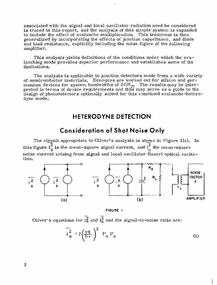
FIGURE I - - 2 2 Oliver's equations for is and in and the signal-to-noise ratio are:
2
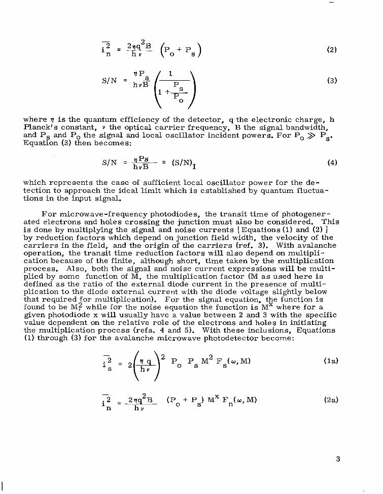
where 9 is the quantum efficiency of the detector, q the electronic charge, h Planck's constant, Y the optical car r ie r frequency, B the signal bandwidth, and P, and Po the signal and local oscillator incident powers. For Po >> Ps. Equation (3) then becomes:
which represents the case of sufficient local oscillator power for the de- tection to approach the ideal limit which is established by quantum fluctua- tions in the input signal.
For microwave-frequency photodiodes, the transit time of photogener- ated electrons and holes crossing the junction must also be considered. is done by multiplying the signal and noise currents [Equations (1) and (2) 1 by reduction factors which depend on junction field width, the velocity of the carriers in the field, and the origin of the ca r r i e r s (ref. 3). With avalanche operation, the transit time reduction factors w i l l also depend on multipli- cation because of the finite, although short, time taken by the multiplication process. Also, both the signal and noise current expressions w i l l be multi- plied by some function of M, the multiplication factor (M a s used here is defined a s the ratio of the external diode current in the presence of multi- plication to the diode external current with the diode voltage slightly below that required for multiplication). For the signal equation, the function is found to be MF while for the noise equation the function is MX where for a given photodiode x w i l l usually have a value between 2 and 3 with the specific value dependent on the relative role of the electrons and holes in initiating the multiplication process (refs. 4 and 5). With these inclusions, Equations (1) through (3) for the avalanche microwave photodetector become:
This
3
where Fs ( w , M ) and Fn (w,M) a re the signal and noise transit-time reduc- tion factors, r e spe ctively.
Equation (2a) can be fitted with x = 2. 5 for the best silicon photodetec- to rs reported, and x = 3 for germanium ones (ref. 6). To a reasonable ap- proximation, Fs ( w , M) and Fn (0, M) can be assumed to be equal:: and cancel each other in Equation (3a). Since x >_ 2, Equation (3a) shows that ava- lanche (M > 1) operation of a photodiode w i l l never allow the S/N ratio to ap- proach (S/N)I, regardless of other diode details and the noise properties of any ancillary amplifier. operation of a heterodyne photodiode offers practical advantages cannot be determined. To answer the question, a practical detection system must first be considered.
However, at this point whether o r not avalanche
Inclusion of Additianal Noise Sources
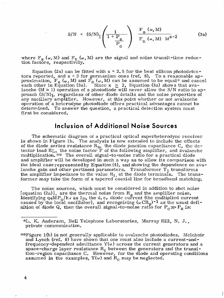
The schematic diagram of a practical optical superheterodyne receiver is shown in Figure lb. of the diode ser ies resistance Rs, the diode junction capacitance C, the de- tector load RL, the noise factor F of the following amplifier, and Avalanche multiplication. :w The overall signal-to-noise ratio for a practical diode and amplifier w i l l be developed in such a way as to allow its comparison with the ideal case represented by Equation (4), and showing the dependence on ava- lanche gain and other pertinent parameters. Transformer T transforms the amplifier impedance to the value RL at the diode terminah. The trans- former may take the form of a tapered coaxial line for broadband matching.
The analysis is now extended to include the effects
The noise sources, which must be considered in addition to shot noise [equation (2a)], a re the thermal noise from Rs and the amplifier noise. Identifying qqMPo/hu as Ip, the d. c.. diode current (the multiplied current caused by the local oscillator), and recognizing (wCRg;)-l as the usual defi- nition of diode Q, then the overall signal-to-noise ratio for Po>>Ps is:
:FL. K. Anderson, Bell Telephone Laboratories, Murray Hill, N. J., private communication.
**Figure 1 (b) is not generally applicable to avalanche photodiodes. Melchoir and Lynch (ref. 6) have shown that one must also include a current-and- frequency-dependent admittance Y ( o ) across the current generators and a space-charge layer resistance Rc between the generators and the transi- tion-region capacitance C. However, for the diode and operating conditions assumed in the examples, Y(w) and Rc may be neglected.
4
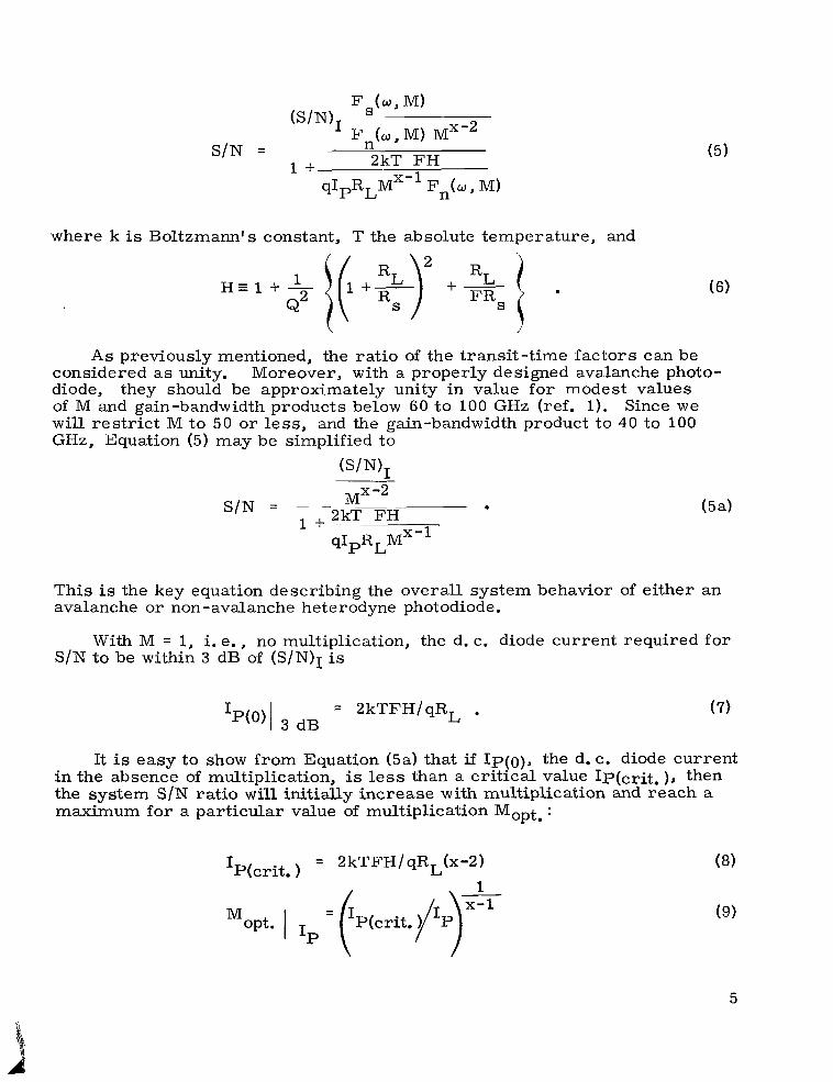
where k is Boltzmann's constant, T the absolute temperature, and
A s previously mentioned, the ratio of the transit-time factors can be considered a s unity. diode, they should be approximately unity in value for modest values of M and gain-bandwidth products below 60 to 100 GHz (ref. 1). Since we w i l l restrict M to 50 or less, and the gain-bandwidth product to 40 to 100 GHz, Equation (5) may be simplified to
Moreover, with a properly designed avalanche photo-
- -
1 +
This is the key equation describing the overall system behavior of either an avalanche or non-avalanche heterodyne photodiode.
S/N to be within 3 dB of (S/N)I is With M = 1, i. e., no multiplication, the d. c. diode current required for
I = 2kTFH/qRL . p ( o ) l 3 dB (7)
It is easy to show from Equation (5a) that if Ip(o), the d. c. diode current in the absence of multiplication, is less than a critical value IP(crit, ), then the system S/N ratio w i l l initially increase with multiplication and reach a maximum for a particular value of multiplication Mopt. :
5
Conversely, for Ip(0) > Ip(crit, ), avalanche multiplication w i l l always decrease the S/N ratio. In the former case, and with M = Mopt.,
( s /N) / ( s /N)~ = (10)
and the relative optical local oscillator power required is:
In Equations (9) through (ll), we have chosenIp, the actual d. c. diode current, as the independent variable rather than Ip(oj, the d. c. diode current which one would observe in the absence of multiplication (Ip(0) = IP/M). This choice w a s made because I p is linearly related to diode dissipation, and also because it may be monitored continuously in an operating system.
A comparison for the general case Ip(0) < Ip(crit. ), the avalanche- heterodyne mode with heterodyne-only operation can now be made. Com- paring Equation (10) (M = Mopt. ) with Equation (5a) for M = 1, it may be noted that (S/N)/(S/N)1 €or M = Mopt. decreases less rapidly a s I p is re - duced. This means that, for a given value of I , and thus a given value of diode dissipation, an optimum choice of multipfication w i l l result in an in- creased signal-to-noise ratio. Alternately, we can conclude from a com- parison of these two equations that, for a desired signal-to-noise ratio, the diode dissipation may be reduced since the latter is proportional to Ip, and this in turn is less for avalanche operation. It is also possible to show that avalanche operation can combine these benefits to yield a simultaneous in- crease in (S/N)/(S/N)1 and decrease in diode dissipation. Of course, i f we require both, then the improvement in either is not so great as it would be if we had chosen to maximize only one.
Finally, it is noted that, for a given diode current, avalanche operation reduces the local oscillator (laser) power required. It is possible to relate to one another in a single graph the quantities discussed: (S/N)/(S/N)1, diode current, diode dissipation, and local oscillator power required; both for M = 1 and for various values of M including Mopt.
designed silicon and germanium detectors. In the next section we shall present the results computed for suitably
EXAM P L ES
In this section, the behavior expected from a suitably operated avalanche- optical superheterodyne receiving system is determined, and then compared with the behavior of a "heterodyne-only" system, using the same components.
6
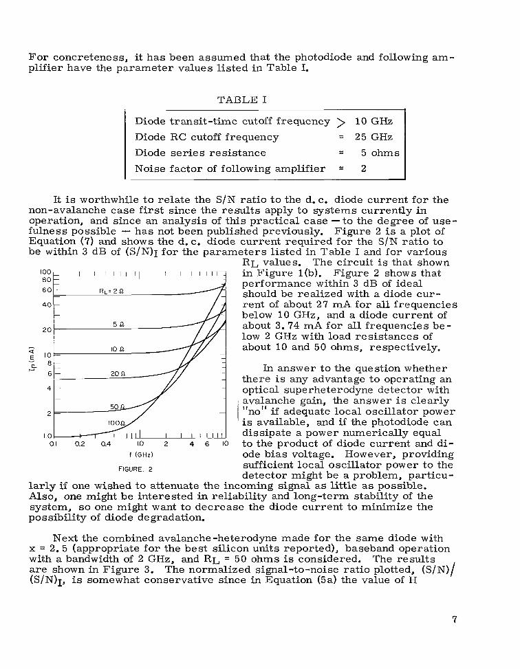
For concreteness, it has been assumed that the photodiode and following am- plifier have the parameter values listed in Table I.
80 6 0
40
Diode Diode Diode Noise
- - performance within 3 dB of ideal should be realized with a diode cur- rent of about 27 m A for all frequencies
- -
- below 10 GHz, and a diode current of
TABLE I
4 - optic a1 superheterodyne detector with avalanche gain, the answer is clearly not1 if adequate local oscillator power
is available, and if the photodiode can
-
1 1 2 - -
1 0 0 I I I I I I I I dissipate a power numerically equal
transit-time cutoff frequency > 10 GHz RC cutoff frequency = 25 GHz ser ies resistance = 5 ohms factor of following amplifier = 2
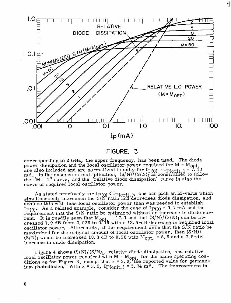
Next the combined avalanche-heterodyne made for the same diode with x = 2.5 (appropriate for the best silicon units reported), baseband operation with a bandwidth of 2 GHz, and RL = 50 ohms is considered. are shown in Figure 3. (S/N)I, is somewhat conservative since in Equation (sa) the value of H
The results The normalized signal-to-noise ratio plotted, (S/N)/
7
- - - - D 1 0 D E DI S S I PAT 10 N - -
&RELATIVE L.O. POWER
I p ( m A )
FIGURE. 3 corresponding to 2 GHz, the upper frequency, has been used. The diode power dissipation and the local oscillator power required for M = Mo t. are also included and are normalized to unity for Ipfo) = Ip(crit, ) = E 4 8 mA. the "M = 1'' curve, and the "relative diode dissipation" curve is also the curve of required local oscillator power.
In the absence of multiplication, (S/N)/ (S/N)I is constramed to follow
A s stated previously for Ip 0) <Ip(crit, , one can pick an M-value which
achieve this with l e s s local oscillator power than was needed to establish Ip(o).. A s a related example, consider the case of Ip(0) = 0. 1 mA and the requirement that the S/N ratio be optimized without an increase in diode cur- rent. It is readily seen that Mopt, = 17. 7 and that (S/N)/(S/N)1 can be in- creased 7.9 dB from 0.026 to 0.16 with a 12.5-dB decrease in required local oscillator power. maximized for the original amount of local oscillator power, then (S/N)/ (S/N)I would be increased 1 0 . 3 dB to 0.28 with Mopt, = 5.6 and a 7.5-dB increase in diode dissipation.
simultaneously increases the S / LI ratio and d ecreases diode dissipation, and
Alternately, if the requirement were that the S/N ratio be
Figure 4 shows (S/N)/ (S/N)I, relative diode dissipation, and relative local oscillator power required with M = Mop for the same operating con- ditions as for Figure 3, except that x = 3 . 0 , hi e reported value for german- iwn photodiodes. With x = 3 . 0 , IP(crit, ) = 3. 74 mA. The improvement in
8
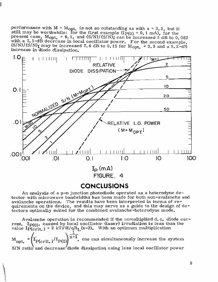
performance with M = Mo t. is not so outstanding as with x = 2.5, but it still may be worthwhile: for the first example (Ip(0) = 0. 1 mA), for the present case, Mopt, = 6.1, and (S/N)/(S/N)I can be increased 5 dB to 0.082 with a 7.5-dB decrease in local oscillator power. For the second example, (S/N)/(S/N)I may be increased 7.6 dB to 0.15 for Mopt, = 3 . 3 and a 5.2-dB increase in diode dissipation.
Ip (mA) FIGURE. 4
CONCLUSIONS An analysis of a p-n junction photodiode operated as a heterodyne de-
tector with microwave bandwidths has been made for both non-avalanche and avalanche operations. quirements on the device, and this may serve a s a guide to the design of de- tector s optimally suited for the combined avalanche -heterodyne mode.
Avalanche operation is recommended if the unmultiplied d. c. diode cur-
The results have been interpreted in te rms of r e -
rent. Ip(o), caused by local oscillator (laser) irradiation is less than the value IP(crit, ) = 2 kTFH/qRL(x-2).
- (" / I ) , one can simultaneously increase the system M
S/N ratio and decrease diode dissipation using l e s s local oscillator power
With an optimum multiplication 1
x-1 -
opt. - 'P(crit.1 P(O)
9
than w a s required t o establish the original diode current. The degree of im- provement possible strongly depends on the value of x, and this is related to the details of the avalanche multiplication process. Examples a re presented for x = 2.5, the value for the best silicon units reported, and x = 3.0, the value reported for germanium photodiodes. F o r these examples, optimum multiplication lies between 3 and 20. baseband operation with bandwidths of several GHz are possible
With such modest multiplication values,
REFERENCES
1. Anderson, L. K. and McMurtry, B. J. : High-speed Photodetectors. Appl. Opt., vol. 5, p. 1573, 1966.
2. Oliver, B. M.: Thermal and Quantum Noise. Proc. I.E.E.E., vol. 53, p. 436, 1965.
3. DiDomenico, Jr. , M., and Svelto, 0. : Solid-state Photodetection: A Comparison between Photodiodes and Photoconductors. Proc. I. E. E. E., vol. 52, p. 136, 1964.
4. Tager, A. S. : Current Fluctuations in a Semiconductor (Dielectric) under the Conditions of Impact Ionization and Avalanche Breakdown. Soviet Physics - Solid State, vol. 6, p. 1919, 1965.
5. Mchtyre, R. J. : Multiplication Noise in Uniform Avalanche Diodes. I.E.E.E. Trans. Electron Devices, vol. ED-13, p. 164, 1966.
6. Melchior, H., and Lynch, W. T. : Signal and Noise Response of High- Speed Germanium Avalanche Photodiodes. I. E. E. E. Trans. Electron Devices, vol. ED-13, p. 829, 1966.
National Aeronautics and Space Administration Electronics Research Center Cambridge, Massachusetts, July 1967
129-02 -05 -14
10 NASA-Langley, 1967 - 26 c - 2 0
“The aeronautical and space activities of the United States shall be conducted JO as to contribute . . . to the expansion of human knowl- edge of phenomena in the atmosphere and space. The Administration shall provide for the widest practicable and appropriate dissemination of information concerning its activities and the results tbereof .”
-NATIONAL h R O N A U n c S AND SPACE ACT OF 1958
NASA SCIENTIFIC AND TECHNICAL PUBLICATIONS
TECHNICAL REPORTS: Scientific and technical information considered important, complete, and a lasting contribution to existing knowledge.
TECHNICAL NOTES: Information less broad in scope but nevertheless of importance as a contribution to existing knowledge.
TECHNICAL MEMORANDUMS: Information receiving limited distribu- tion because of preliminary data, security classification, or other reasons.
CONTRACTOR REPORTS: Scientific and technical information generated under a NASA contract or grant and considered an important contribution to existing knowledge.
TECHNICAL TRANSLATIONS: Information published in a foreign language considered to merit NASA distribution in English.
SPECIAL PUBLICATIONS: Information derived from or of value to NASA activities. Publications include conference proceedings, monographs, data compilations, handbooks, sourcebooks, and special bibliographies.
TECHNOLOGY UTILIZATION PUBLICATIONS: Information on tech- nology used by NASA that may be of particular interest in commercial and other non-aerospace applications. Publications include Tech Briefs, Technology Utilization Reports and Notes, and Technology Surveys.
Details on the availability of these publications may be obtained from:
SCIENTIFIC AND TECHNICAL INFORMATION DIVISION
N AT1 0 N A L A E R 0 N A UTI CS A N D SPA C E A D M I N I STR AT IO N
Washington, D.C. PO546