Embed Size (px)
Citation preview

Characterization of Two Thin Postion-Sensitive
Avalanche Photodiodes on a Single Flex Circuit for
Use in 3-D Positioning PET DetectorsAngela M K Foudray, Student Member, IEEE, Richard Farrell, Member, IEEE,
Peter D Olcott, Student Member, IEEE, Kanai S Shah, Member, IEEE, and Craig S Levin, Member, IEEE
Abstract— We are developing 1 mm resolution, 3-D positioning,high sensitivity positron emission tomography imaging systemsfor small animal and breast-dedicated imaging applications.The system uses detector modules that comprises two adjacentposition-sensitive avalanche photodiodes (PSAPDs), each with asegmented lutetium oxyorthosilicate (LSO) scintillation crystalarray, mounted on a single flex cable readout circuit. The moduleis oriented two PSAPDs deep in the depth of interaction direction,which facilitates high photon sensitivity (∼2 cm of LSO). Inthis study, we are testing two PSAPD chips in a single flex-cable module simultaneously to investigate their performance andaccess the degree of inter-device cross-talk. The inter-device cross-talk was measured by looking at the signal in an un-irradiatedPSAPD chip while the adjacent PSAPD chip was irradiated,both chips under bias. The signal was three orders of magnitudelower in the unirradiated PSAPD versus the irradiated PSAPD. Individual crystal energy resolution for an array coupled to aPSAPD was measured to be 10.03 ± 4.45% for the 1mm x 1mm x3mm array. All crystals were resolved in a flood histogram, withan average peak-to valley ratio of ∼11, with the lowest PVRbeing 1.8. The average coincidence time resolution was 3.75nsFWHM across the devices. These measurements indicate thatdegradation due to the close proximity of two PSAPDs on thesame readout circuit is small.
Index Terms— PSAPD, LSO, Edge-On, 3D, characterization,flex-cable, RMD, APD
I. INTRODUCTION
THE small size, high quantum efficiency, and high spatial
resolution of semiconductor photodetectors when cou-
pled to the high-Z scintillator crystals commonly used in
positron emission tomography (PET) have made them good
candidates for use in detector systems. A novel position-
sensitive avalanche photodiode (PSAPD) [1] has been devel-
oped by Radiation Monitoring Devices, Inc. and studied when
packaged individually on a flex-cable readout circuit in our
previous work [2].
Manuscript received November 17, 2006. This work was supported inpart by NIH-National Cancer Institute R21 CA098691, NIH-NIBIB R21EB003283, NIH-NCI CA119056 grants and PEO International Scholar Award.
Angela MK Foudray is a student at the University of California-San Diego,Department of Physics, La Jolla, CA, USA and is working in the Departmentof Radiology, the Molecular Imaging Program at Stanford University (email:[email protected]).
Peter Olcott and Craig S Levin are in the Department of Radiology andthe Molecular Imaging Program at Stanford University, Palo Alto, CA, USA(email: [email protected], [email protected] and [email protected]).
Richard Farrell and Kanai Shah are at Radiation Monitoring Devices, Inc.in Watertown, MA
Fig. 1. Shown is a portion of the designed system; 8 modules are stackedand then repeated in three columns. In the figure a red photon is incident, themodules consist of grey LSO crystal sitting atop two dark grey PSAPDs (1cmx 1cm) and yellow flexcable. The top row of crystals are opaque, showingtheir relative location; and the rest of the levels are transparent, showing thePSAPD underneath. In this geometry, incoming photons see a minimum of 2cm thick LSO.
In order to increase the stopping efficiency and effective
photon sensitivity of a detector system based on this technol-
ogy, we have designed and tested a module that consists of two
thin PSAPDs mounted on a single flex cable readout circuit
(see illustration of a portions of the system in Fig. 1).
Fig. 2. Picture of two silicon chipPSAPDs (black squares) on oneflex cable (yellow material). Themodule is mounted to glass withtape to rigidly secure the structureduring movement and coupling toacquisition electronics.
Previously, we have tested
a flex-circuit with a single
PSAPD chip mounted on a
flex-cable readout circuit [2].
In this study, we are test-
ing two chips mounted on a
single flex-cable, and the de-
gree of inter-device cross-talk
expected due to their close-
proximity. In a single module,
the chips are only ∼ 50µm
apart, both very sensitive to
ambient EM fields and require
about 1700 Volts of biasing
voltage. It is not obvious that
the performance characteristics
of each of the PSAPDs on
this dual-chip version will be
same as that achieved by one
PSAPD chip mounted on the
flex-circuit. Energy, spatial and
coincidence time resolution were measured with both devices
biased. One of the modules that we have tested is pictured in
Fig. 2.
2006 IEEE Nuclear Science Symposium Conference Record M11-89
1-4244-0561-0/06/$20.00 ©2006 IEEE. 2469
Authorized licensed use limited to: Stanford University. Downloaded on May 25,2010 at 16:27:05 UTC from IEEE Xplore. Restrictions apply.

II. METHODS
A high-voltage supply and readout board was constructed
to read-out and deliver bias to the two PSAPDs through the
single flex-circuit. Positioning for the PSAPD is calculated
using signals from the four corner anodes shown in Fig. 3,
using the following standard Anger-type logic formula:
X =(A + B) − (C + D)
A + B + C + D(1)
Y =(A + D) − (B + C)
A + B + C + D(2)
where A, B, C, and D are the digitized four corner anode
signals of the PSAPD; X and Y are the coordinates of the
scintillation light centroid on the PSAPD surface. Either A,B,C
and D are summed or the common signal is read to obtain the
energy of an event.
Fig. 3. Illustration of the four corner positioning anodes (A,B,C and D) andthe common cathode. The inorganic scintillator (LSO) is optically coupled tothe PSAPD with grease and then wrapped with Teflon as a reflector material(not shown).
All measurements were made using a 10 µCi, 500µm
diameter, 22Na point source. The same array of 1x1x3 mm3
lutetium oxyorthosilication (LSO) crystals was optically cou-
pled to both of the PSAPDs on the flex cable for each study
performed. The crystals were coupled by one of their 1x3
mm2 faces, to form a 8x3 crystal array, 8mm x 9mm in
area, on the face of the device. The array was wrapped in
12 layers of Teflon to provide a reflective surface, but had no
reflective material between the individual crystal elements. For
each measurement, both devices were biased together, with the
same voltage supply. Parameter optimization experiments have
determined optimal device operation is obtained with a bias
between 1680 and 1760 V.
Spatial crystal identification was measured for the devices
by using flood irradiation and by acquiring the four spatial
channels of the irradiated device. Events were triggered by
the sum of the four corner channels. Energy resolution was
determined by fitting two gaussians to the photopeak - one for
511 keV events, and one for 511 keV - 63 keV events where
the 63 keV x-ray produced in the photoelectric interaction
escaped the crystal. Being that these crystals are tiny, an x-
ray escaping the crystal of interaction happens a measurable
amount of the time.
Coincidence time resolution was measured using the same22Na point source between the PSAPD, in alignment with a
1cm diameter Hamamatsu H3164 photomultiplier tube (PMT),
which had a 3mm x 3mm x 8 mm piece of LSO cystal attached
as the scintillation material. The events were triggered by a
timing seperation of less than 50 nanoseconds between an
energy gated common signal of the PSAPD and an energy
gated 8th (last) dynode signal of the PMT.
Cross talk was measured in two ways: (1) by acquiring
spatial signals for one of the devices on a flex-circuit while
irradiating a crystal array coupled to the other PSAPD and (2)
by acquiring spatial signals from the irradiated device as well
as the common channel of the unirradiated device.
III. RESULTS AND DISCUSSION
A. Crosstalk
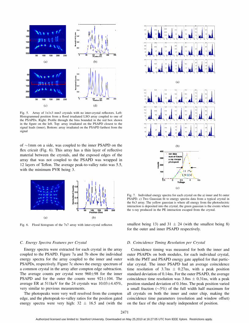
(a) (b)
(c) (d)
Fig. 4. Top, Left: Signals from the corner anodes for the irradiated devicewith an LSO array of 2x2x3 mm3 crystals and, Top, Right: adjacent PSAPDchip device with no LSO crystal coupled to it. The black line is the sum of thefour corner anodes, which are shown in magenta, red, green and blue. Bottom,Left: The sum of the corner signals (black), compared to the common signalfrom the un-irradiated device with no crystal coupled (magenta). Bottom,Right: Signals from the 4 corner channels compared to the common channel(black) of the un-irradiated device.
Cross talk between the two devices was measured and is
compared in figure 4 with the data acquired in both PSAPDs
for the same acquisition time. The number of events recorded
in the non-irradiated compared to the irradiated PSAPD was
three orders of magnitude lower across all energies, including
in the photopeak. This is an indicator that the devices are
electrically isolated relatively well from one another, i.e.,
readout or current generation from one device will not in
general trigger a spurious event from the neighboring chip.
B. Crystal Identification
Shown in Fig. 5 are typical results of flood irradiation of
segmented LSO arrays optically coupled to one of the PSAPD
chips with both chips biased. Figure 5 is an 8x3 array of
1x1x3 mm3 crystals, with no inter-crystal reflector, coupled
to each of the PSAPDs on one dual-chip module. Crystals
are identified and results are comparable to previous results
achieved with one PSAPD per module. Profiles were taken
through the middle row of each array shown on the left hand
side of Fig. 5. The average peak to valley ratio for the inner
chip was 11.3 and was 10.9 for the outer chip.
For comparison, a segmented crystal array manufactured by
Agile Engineering, made of LSO, each crystal having a size
2470
Authorized licensed use limited to: Stanford University. Downloaded on May 25,2010 at 16:27:05 UTC from IEEE Xplore. Restrictions apply.
(a) (b)
(c) (d)
Fig. 5. Array of 1x1x3 mm3 crystals with no inter-crystal reflectors. Left:Histogrammed position from a flood irradiated LSO array coupled to one ofthe PSAPDs. Right: Profile through the bins bounded in the red box shownin the figure on the left. Top: array irradiated on the PSAPD closest to thesignal leads (inner), Bottom: array irradiated on the PSAPD farthest from thesignal
of ∼1mm on a side, was coupled to the inner PSAPD on the
flex cricuit (Fig. 6). This array has a thin layer of reflective
material between the crystals, and the exposed edges of the
array that was not coupled to the PSAPD was wrapped in
12 layers of Teflon. The average peak-to-valley ratio was 5.5,
with the minimum PVR being 3.
(a) (b)
Fig. 6. Flood histogram of the 7x7 array with inter-crystal reflector.
C. Energy Spectra Features per Crystal
Energy spectra were extracted for each crystal in the array
coupled to the PSAPD. Figure 7a and 7b show the individual
energy spectra for the array coupled to the inner and outer
PSAPDs, respectively. Figure 7c shows the energy spectrum of
a common crystal in the array after compton edge subtraction.
The average counts per crystal were 960±98 for the inner
PSAPD and for the outer the counts were 921±104. The
average ER at 511keV for the 24 crystals was 10.03±4.45%,
very similar to previous measurements.
The photopeaks were very well resolved from the compton
edge, and the photopeak-to-valley ratios for the position gated
energy spectra were very high: 32 ± 16.5 and (with the
(a)
(b)
(c)
Fig. 7. Individual energy spectra for each crystal on the a) inner and b) outerPSAPD. c) Two Guassian fit to energy spectra data from a typical crystal inthe 8x3 array. The yellow gaussian is where all energy from the photoelectricinteraction is deposited into the crystal, the green gaussian is the events wherethe x-ray produced in the PE interaction escaped from the crystal.
smallest being 13) and 31 ± 24 (with the smallest being 8)
for the outer and inner PSAPD respectively.
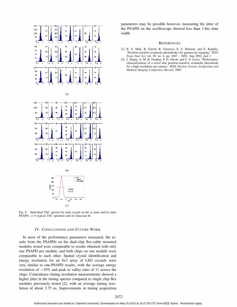
D. Coincidence Timing Resolution per Crystal
Coincidence timing was measured for both the inner and
outer PSAPDs on both modules, for each individual crystal,
with the PMT and PSAPD energy gate applied for that partic-
ular crystal. The inner PSAPD had an average coincidence
time resolution of 3.7ns ± 0.27ns, with a peak position
standard deviation of 0.14ns. For the outer PSAPD, the average
coincidence time resolution was 3.8ns ± 0.31ns, with a peak
position standard deviation of 0.16ns. The peak position varied
a small fraction (∼5%) of the full width half maximum for
all crystals on both the inner and outer chip, making the
coincidence time parameters (resolution and window offset)
on the face of the chip nearly independent of position.
2471
Authorized licensed use limited to: Stanford University. Downloaded on May 25,2010 at 16:27:05 UTC from IEEE Xplore. Restrictions apply.
(a)
(b)
(c)
Fig. 8. Individual TAC spectra for each crystal on the a) inner and b) outerPSAPD. c) A typical TAC spectrum and its Gaussian fit.
IV. CONCLUSIONS AND FUTURE WORK
In most of the performance parameters measured, the re-
sults from the PSAPDs on the dual-chip flex-cable mounted
modules tested were comparable to results obtained with only
one PSAPD per module, and both chips on one module were
comparable to each other. Spatial crystal identification and
energy resolution for an 8x3 array of LSO crystals were
very similar to one-PSAPD results, with the average energy
resolution of ∼10% and peak to valley ratio of 11 across the
chips. Coincidence timing resolution measurements showed a
higher jitter in the timing spectra compared to single chip flex
modules previously tested [2], with an average timing reso-
lution of about 3.75 ns. Improvements in timing acquisition
parameters may be possible however, measuring the jitter of
the PSAPD on the oscilloscope showed less than 1.8ns time
width.
REFERENCES
[1] K. S. Shah, R. Farrell, R. Grazioso, E. S. Harmon, and E. Karplus,“Position-sensitive avalanche photodiodes for gamma-ray imaging,” IEEE
Trans Nucl Sci, vol. 49, no. 4, pp. 1687 – 1692, Aug 2002, part 1.[2] J. Zhang, A. M. K. Foudray, P. D. Olcott, and C. S. Levin, “Performance
characterization of a novel thin position-sensitive avalanche photodiodefor a high resolution pet camera,” IEEE Nuclear Science Symposium and
Medical Imaging Conference Record, 2005.
2472
Authorized licensed use limited to: Stanford University. Downloaded on May 25,2010 at 16:27:05 UTC from IEEE Xplore. Restrictions apply.