Embed Size (px)
Citation preview

9. Optical methods in defect investigations
Hartmut S. Leipner: Structure of imperfect materials
Optical transitions in solidsAbsorption and emission linesConfiguration–coordination diagramLocal vibrational modesIR spectrometerRaman spectroscopy

hsl 2008 – Structure of imperfect materials – Optical methods
Optical methods
Standard methods for the characterization of materials are the absorption/reflection of light or the investigation of emitted light after excitation Analysis of absorption or emission bands (energy position, line shape, temperature dependence) allows defect characterization (lattice coupling, deep/shallow traps, intra/interband recombination)
Determination of the defect density only via comparison with reference methods/standards
2

hsl 2008 – Structure of imperfect materials – Optical methods
Absorption coefficient I(x) = I(0)e−αx
Energy transitions in semiconductors with a direct or and indirect bandgap
hν = Ef − Ei − Ephν = Ef − EiEg
E E
k k
Eg
Fundamental absorption
3

hsl 2008 – Structure of imperfect materials – Optical methods
Direct bandgap:α ∝ (hν − Eg)1/2
Empirically often Urbach’s rule fulfilled:
Reason [Dow, Redfield 1972]: internal electric fields due to impurities and other defects; phonon scattering
Indirect bandgap:
(phonon absorption)
(phonon emission)
α(hν) = αa + αe(phonon emission and absorption forhν > Eg + Ep)
Absorption coefficient
4

hsl 2008 – Structure of imperfect materials – Optical methods
Absorption edge of GaAs at 300 K [Bleicher 1986]
Empirical definition of the absorption edge:Point of the strongest change in α
Abs
orpt
ion
coef
ficie
nt α
Photon energy hν
MeasurementCalculation
Absorption edge
5

hsl 2008 – Structure of imperfect materials – Optical methods
Ionization of a shallow donor and a shallow acceptor by light absorption (EI ionization energy)
D0 → D+ + e− A0 → A− + h+
hν
hνDonor D
Acceptor A
Band–impurity transitions
6

hsl 2008 – Structure of imperfect materials – Optical methods
The ionization energy EI of a shallow state can be obtained with the hydrogen model (effective mass model)
(typically 10 … 100 meV)
Absorption of Si in the far infrared region at 4.2 K due to boron
[Burstein et al. 1956/Bleicher 1986]
αI = σd(Nd − ne) for donorsαI = σa(Na − ph) for acceptors
Capture cross section
Abs
orpt
ion
coef
ficie
nt
Photon energy
Abs
orpt
ion
coef
ficie
nt
Photon energy
Ionization energy
7

hsl 2008 – Structure of imperfect materials – Optical methods
Scheme of different radiative transitions between the conduction band (EC), the valence band (EV), exciton (EE), donor (ED), and acceptor levels (EA).
Optical transitions
8

hsl 2008 – Structure of imperfect materials – Optical methods
Radiative recombination transitions
(1) Intraband transition (phonon assisted emission of light or pure phonon process(2) Interband transition hν » Eg, thermal distribution of carriers gives a broad emission spectrum(3) Exciton decay; free or bound excitons are possible (X, D0X, A0X, D+X, A−X)(4,5) Extrinsic luminescence under participation of donors or acceptors, e. g. e− + A0 → A− + hν(6) Donor–acceptor pair luminescence (DA), D0 + A0 → D+ + A− + hν(7) Recombination under participation of intra-defect transitions, Z* → Z + hν (Z* excited state of the defect Z)
9

hsl 2008 – Structure of imperfect materials – Optical methods
Multiphonon emission, hν = nhΩ
Auger effect (photon energy is transferred to a second electron)
Recombination at surface states or (extended) defects
Nonradiative recombination
10
hsl 2008 – Structure of imperfect materials – Optical methods
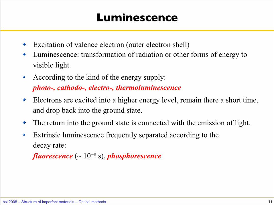
Excitation of valence electron (outer electron shell)Luminescence: transformation of radiation or other forms of energy to visible lightAccording to the kind of the energy supply: photo-, cathodo-, electro-, thermoluminescenceElectrons are excited into a higher energy level, remain there a short time, and drop back into the ground state.
The return into the ground state is connected with the emission of light.Extrinsic luminescence frequently separated according to the decay rate: fluorescence (~ 10−8 s), phosphorescence
Luminescence
11

hsl 2008 – Structure of imperfect materials – Optical methods
Sample absorption and emission spectrum at 77 K of a dye[Zhmyreva, Reznikova 1961/Nelkowski 1992]
Wavenumber (103 cm−1)
Wavelength (nm)
Nor
mal
ized
inte
nsity
Absorption and emission lines
12

hsl 2008 – Structure of imperfect materials – Optical methods
Energy states of an F center in NaCl. The full lines were calculated for absorption, the dashed lines for emission.
[Scherz 1992]
Photon emissionPhoton absorption
Stokes shift
13

hsl 2008 – Structure of imperfect materials – Optical methods
Optical transitions
Stokes shift: Due to electron–lattice coupling excitation of electrons changes vibrational properties of a defect → new equilibrium position, shift in electron levelsBorn–Oppenheimer approximation: Electrons move very fast and follow immediately (adiabatically) the slow motion of atoms.Consequence is the Frank–Condon principle: Electronic transitions take place much faster than the nuclei can respond.
14

hsl 2008 – Structure of imperfect materials – Optical methods
According to the Frank–Condon principle, the most intense vibronic transition is from the ground vibrational state to the vibrational state lying vertically above it. Transitions to other vibrational levels may also occur, but with much lower intensity.
Vertical transition
15

hsl 2008 – Structure of imperfect materials – Optical methods
In the quantum mechanical version of the Frank–Condon principle, the molecule (defect) undergoes a transition to the upper vibrational state (*) that most closely resembles the vibrational wavefunction of the vibrational ground state of the lower electronic state. The two wavefunctions shown here have the greatest overlap integral of all the vibrational states of the upper electronic state and hence are most closely similar.
Position
Tota
l ene
rgy
Frank–Condon principle quantum mechanically
16

hsl 2008 – Structure of imperfect materials – Optical methods
Frank–Condon principle:Transition time for the electron is much shorter than the relaxation time of the system to reach the new equilibrium state
hΩ
Configuration coordinate diagram
17
hsl 2008 – Structure of imperfect materials – Optical methods
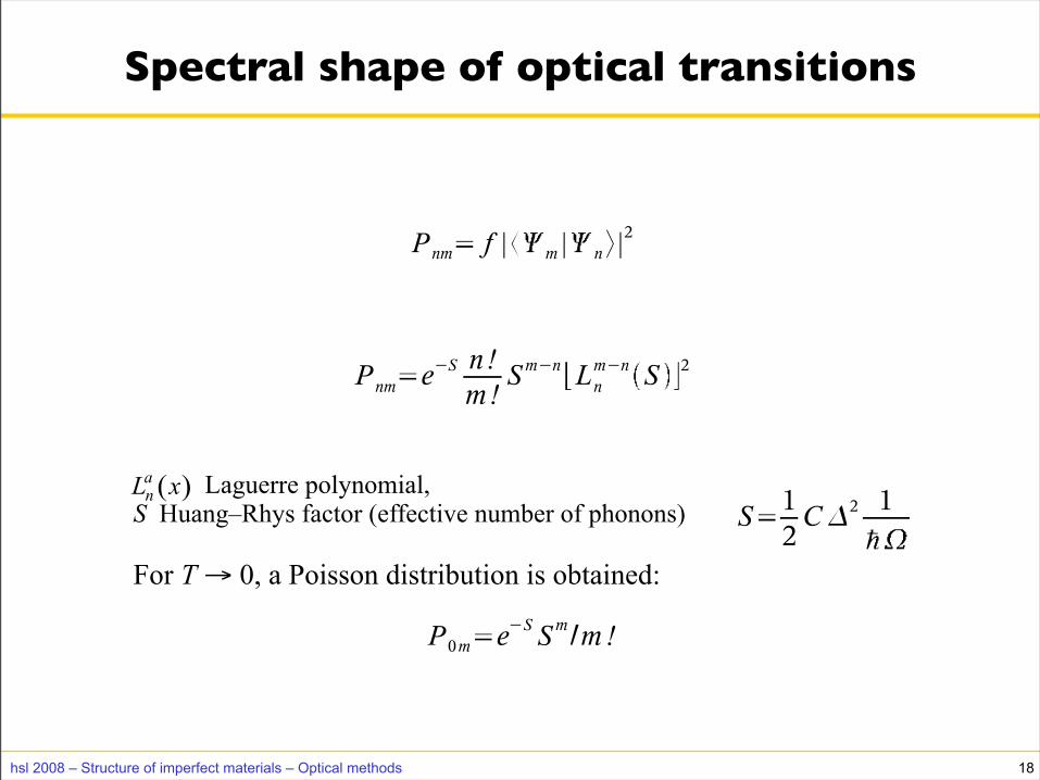
Laguerre polynomial, S Huang–Rhys factor (effective number of phonons)
For T → 0, a Poisson distribution is obtained:
Spectral shape of optical transitions
18

hsl 2008 – Structure of imperfect materials – Optical methods
Line shapes in the photoluminescence for different Huang–Rhys coupling parameters S. The maximum intensity for m = S is normalized to 1. The energy of the zero phonon line is indicated as E0.
PL
inte
nsity
PL
inte
nsity
PL
inte
nsity
PL
inte
nsity
E0
E0 E0
E0
Photoluminescence lines
19

hsl 2008 – Structure of imperfect materials – Optical methods
50 µm 20 µm
Dislocations in CdTe
Low-temperature luminescence near dislocations in cadmium telluride
20

hsl 2008 – Structure of imperfect materials – Optical methods
1.40 1.45 1.50 1.55 1.60
Dislocation rosette Matrix
DL
Wavelength (nm)
CL
inte
nsity
(arb
itrar
y un
its)
Photon energy (eV)
900 850 800
Cathodoluminescence spectra at 4 K in CdTe
21

hsl 2008 – Structure of imperfect materials – Optical methods
Vibration of a center, even if it is nonpolar may result in an oscillating dipole that can interact with the electromagnetic fieldSelection rule: Vibration is infrared active if the electric dipole moment changes by the displacement, otherwise no interaction with the electromagnetic field is possible.Identification of the symmetry species of a normal mode
Local vibrational modes
22

hsl 2008 – Structure of imperfect materials – Optical methods
Different vibrational modes of a CO2 and a H2O molecule. The stretching and bending normal modes with the corresponding wave numbers are shown.
Identification of vibrational modes
23

hsl 2008 – Structure of imperfect materials – Optical methods
Comparison of the data of a cluster calculation with the experimentally resolved structure of the 12CAs LVM line in GaAs (4.2 K; 0.03 cm−1 resolution). The theoretical bars have been broadened by a Lorentzian function to simulate the measurements.
[Gledhill et al. 1991/Newman 1993]
LVM of carbon in GaAs
24

hsl 2008 – Structure of imperfect materials – Optical methods
1 IR source unit, 2 globar, 3 optical microprobe, 4 sample, 5 mirror lenses, 6 spectrometer unit, 7 entrance slit, 8 NaCl prism, 9 detector unit, 10 bolometer, 11 exit window, 12 cryostat, 13 cryostat windows, 14 sample, 15 PbS cell.
IR spectrometer
25

hsl 2008 – Structure of imperfect materials – Optical methods
A Michelson interferometer as the main element of an FTIR spectrometer. The beam-splitting element divides the incident beam into two beams with a path difference that depends on the location of the mirror M1. The compensator ensures that both beams pass through the same thickness of material.
FTIR spectrometer
26

hsl 2008 – Structure of imperfect materials – Optical methods
Intensity of the detected signal due to radiation in the range of wave numbers ν to ν + dν ,
dI(p,ν) = I(ν)(1 + cos 2πνp)dν(The spectrometer converts the presence of a particular frequency
component into a variation in intensity reaching the detector.)
Fourier transformation to obtain the absorption spectrum I(ν),
Major advantage of FTIR spectroscopy: all the radiation emitted by the source is monitored continuously; resulting in a higher sensitivity
Resolution:
Fourier transformation spectroscopy
27

hsl 2008 – Structure of imperfect materials – Optical methods
The three frequency components and their intensities that account for the appearance of the interferogram on the left. This spectrum is the Fourier transform of the interferogram, and is a depiction of the contributing frequencies.
An interferogram obtained when several (in this case 3) frequencies are present in the radiation.
Inte
nsity
I(ν)
Wavenumber νpν
FTIR spectrum
28

hsl 2008 – Structure of imperfect materials – Optical methods
Additional lines with frequencies ω0 ± Ω are found in the scattered light, when a molecule is illuminated with monochromatic light ω0 (C. V. Raman 1928).Inelastic scattering, transition between energy levels of molecular vibrationCharacteristic frequencies ωR depend on excitation of vibrational modes in the sample.Inelastic scattering of a photon in the crystal by formation (Stokes process) or annihilation of a phonon (anti-Stokes process) ω0 = ω0 ± Ω; k = k’ ± K
Raman effect
29

hsl 2008 – Structure of imperfect materials – Optical methods
Induced dipole moment by the illumination, p = αℰElectrical field ℰ = ℰ0 sin ω0tVibrations of the molecule cause periodic changes in the polarizability α = α0 + α1 sin ΩtIt follows for the induced dipole momentp = α0ℰ0 sin ω0t + α1 ℰ0 sin ω0t sin Ωt orp = α0ℰ0 sin ω0t + ½ α1 ℰ0 [cos (ω0 – Ω)t – cos (ω0 + Ω)t]
Rayleigh line anti-Stokes line Stokes line
Polarization
30

hsl 2008 – Structure of imperfect materials – Optical methods
A possible arrangement adopted in Raman spectroscopy. The scattered radiation is monitored at right angles to the incident radiation.
Raman spectroscopy
31

hsl 2007 – Structure of imperfect materials – X-ray methods
References
M. Bleicher: Halbleiter-Optoelektronik. Berlin: Verlag Technik 1986.H. Nelkowski in: Bergmann Schäfer Lehrbuch der Experimentalphysik, Vol. 6. Ed. W. Raith. Berlin: de Gruyter 1992, p. 621.U. Scherz in: Bergmann Schäfer Lehrbuch der Experimentalphysik, Vol. 6. Ed. W. Raith. Berlin: de Gruyter 1992, p. 1.P. Atkins: Physical Chemistry. New York: Freeman 1998.W. Stadler: Defekte Und Kompensation in II–VI-Halbleitern. Dissertation Technische Universität München 1995.R. C. Newman: Semicond. Semimet. 38 (1993) 117.