Embed Size (px)
Citation preview
A product of a PHYTEC Technology Holding company
nanoMODUL-STM32F103
HHHHARDWARE ARDWARE ARDWARE ARDWARE MMMMANUALANUALANUALANUAL
EEEEDITION DITION DITION DITION AAAAPRILPRILPRILPRIL 2002002002009999
nanoMODUL-STM32F103
PHYTEC Messtechnik GmbH 2009 L-733-e_0
In this manual are descriptions for copyrighted products that are not explicitly indicated
as such. The absence of the trademark () and copyright () symbols does not imply that a product is not protected. Additionally, registered patents and trademarks are similarly not expressly indicated in this manual. The information in this document has been carefully checked and is believed to be entirely reliable. However, PHYTEC Messtechnik GmbH assumes no responsibility for any inaccuracies. PHYTEC Messtechnik GmbH neither gives any guarantee nor accepts any liability whatsoever for consequential damages resulting from the use of this manual or its associated product. PHYTEC Messtechnik GmbH reserves the right to alter the information contained herein without prior notification and accepts no responsibility for any damages which might result. Additionally, PHYTEC Messtechnik GmbH offers no guarantee nor accepts any liability for damages arising from the improper usage or improper installation of the hardware or software. PHYTEC Messtechnik GmbH further reserves the right to alter the layout and/or design of the hardware without prior notification and accepts no liability for doing so.
Copyright 2009 PHYTEC Messtechnik GmbH, D-55129 Mainz. Rights - including those of translation, reprint, broadcast, photomechanical or similar reproduction and storage or processing in computer systems, in whole or in part - are reserved. No reproduction may occur without the express written consent from PHYTEC Messtechnik GmbH.
EUROPE NORTH AMERICA
Address: PHYTEC Technologie Holding AG Robert-Koch-Str. 39 D-55129 Mainz GERMANY
PHYTEC America LLC 203 Parfitt Way SW, Suite G100 Bainbridge Island, WA 98110 USA
Ordering Information:
+49 (800) 0749832 [email protected]
1 (800) 278-9913 [email protected]
Technical Support:
+49 (6131) 9221-31 [email protected]
1 (800) 278-9913 [email protected]
Fax: +49 (6131) 9221-33 1 (206) 780-9135
Web Site: http://www.phytec.de http://www.phytec.com
Preliminary Edition April 2009
Contents
PHYTEC Messtechnik GmbH 2009 L-733-e_0
1 Preface.......................................................................................1
1.1 Introduction .........................................................................3
1.2 Block Diagram ....................................................................4
1.3 View of the nanoMODUL-STM32F103 ...............................5
2 Pin Description .........................................................................7
3 Jumpers...................................................................................13
4 Power Requirements..............................................................16
5 System Memory ......................................................................17
5.1 Memory Model ..................................................................18
5.2 External SRAM (U2) .........................................................19
5.3 I²C EEPROM (U6) ............................................................20
5.3.1 Setting the EEPROM Lower Address
Bits (J7, J8, J9) .....................................................21
5.3.2 EEPROM Write Protection Control (J6)................22
5.4 RS-232 Transceiver (U5)..................................................23
6 JTAG Interface (X1) ................................................................25
7 Technical Specifications........................................................26
8 nanoMODUL-STM32F103 Baseboard ...................................27
Index ................................................................................................29
nanoMODUL-STM32F103
PHYTEC Messtechnik GmbH 2009 L-733-e_0
Index of Figures
Figure 1: Block Diagram of the nanoMODUL-STM32F103 .............4
Figure 2: Top view of the nanoMODUL-STM32F103
(controller side) .................................................................5
Figure 3: Bottom view of nanoMODUL-STM32F103
(connector side) ................................................................6
Figure 4: Pin-out of the nanoMODUL-Connector
(top view, with cross section insert) ..................................8
Figure 5: Typical jumper pad numbering scheme..........................13
Figure 6: Jumper locations (top view) ............................................14
Contents
PHYTEC Messtechnik GmbH 2009 L-733-e_0
Index of Tables
Table 1: Pin-out of the nanoMODUL-Connector.............................9
Table 2: Jumper settings ..............................................................15
Table 3: EEPROM I²C address via J7, J8 and J9.........................21
Table 4: EEPROM write protection states via J6..........................22
nanoMODUL-STM32F103
PHYTEC Messtechnik GmbH 2009 L-733-e_0
Preface
PHYTEC Messtechnik GmbH 2009 L-733e_0 1
1 Preface
This hardware manual describes the nanoMODUL-STM32F103’s design and function. Precise specifications for the ST STM32F103ZE microcontrollers can be found in the enclosed microcontroller Data Sheet/User's Manual. In this hardware manual and in the attached schematics, active low signals are denoted by a "/" or “#” preceding the signal name (e.g.: /RD or #RD). A "0" indicates a logic zero or low-level signal, while a "1" represents a logic one or high-level signal.
Declaration of Electro Magnetic Conformity of the PHYTEC
nanoMODUL-STM32F103
PHYTEC Single Board Computers (henceforth products) are designed for installation in electrical appliances or as dedicated Evaluation Boards (i.e.: for use as a test and prototype platform for hardware/software development) in laboratory environments.
Caution:
PHYTEC products lacking protective enclosures are subject to damage by ESD and, hence, may only be unpacked, handled or operated in environments in which sufficient precautionary measures have been taken in respect to ESD-dangers. It is also necessary that only appropriately trained personnel (such as electricians, technicians and engineers) handle and/or operate these products. Moreover, PHYTEC products should not be operated without protection circuitry if connections to the product's pin header rows are longer than 3 m. PHYTEC products fulfill the norms of the European Union’s Directive for Electro Magnetic Conformity only in accordance to the descriptions and rules of usage indicated in this hardware manual (particularly in respect to the pin header row connectors, power connector and serial interface to a host-PC). Implementation of PHYTEC products into target devices, as well as user modifications and extensions of PHYTEC products, is subject to renewed establishment of conformity to, and certification of, Electro Magnetic Directives. Users should ensure conformance following any modifications to the products as well as implementation of the products into target systems.
The nanoMODUL-STM32F103 is one of a series of PHYTEC nano-/micro-/miniMODULs which can be populated with different controllers and, hence, offers various functions and configurations. PHYTEC supports a variety of 8-/16- and 32-bit controllers in two ways: (1) as the basis for Rapid Development Kits which serve as a reference and evaluation platform (2) as insert-ready, fully functional phyCORE OEM modules, which can be embedded directly into the user’s peripheral hardware design. PHYTEC's microcontroller modules allow engineers to shorten development horizons, reduce design costs and speed project concepts from design to market. For more information go to:
http://www.phytec.com/services/phytec-advantage.html

nanoMODUL-STM32F103
2 PHYTEC Messtechnik GmbH 2009 L-733e_0
Introduction
PHYTEC Messtechnik GmbH 2009 L-733e_0 3
1.1 Introduction
The nanoMODUL-STM32F103 offers the following features:
• Single Board Computer in the size 38 x 47 mm achieved through modern SMD technology
• populated with the STMicroelectronics STM32F103ZE microcontroller (BGA-144 packaging)
• improved interference safety achieved through multi-layer PCB technology and dedicated Ground pins
• controller signals and ports extend to two 60-pin 1,27 mm Samtec connectors aligning two sides of the board, enabling it to be plugged like a "big chip" into target application
• max. 72 MHz clock frequency
• 512 kByte Controller internal Flash1
• 64 kByte Controller internal SRAM
• Up to 2 MByte external SRAM1
• 4kB I²C EEPROM
• Up to 85 GPIOs
• 3 x 12-bit ADCs with up to 16 channels
• 2 channels 12-bit DAC
• 2,5 V external voltage reference
• USB Full Speed Client or CAN 2.0B interface
• Dual RS-232 transceiver (one for using USART1 and internal Bootloader)
• I²C, SPI, I²S, U(S)ART, SDIO
• RTC, Timer, PWM, Watchdog
• one operating voltage for core & peripherals, 3.3 V
• different low power modes
• operating temperature: -40 to 85°C
1 : Please contact PHYTEC for more information about additional module configurations.
nanoMODUL-STM32F103
4 PHYTEC Messtechnik GmbH 2009 L-733e_0
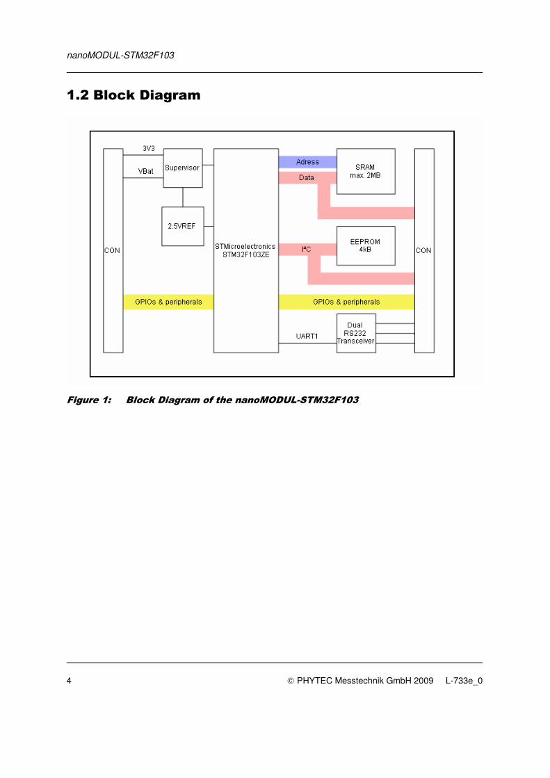
1.2 Block Diagram
Figure 1: Block Diagram of the nanoMODUL-STM32F103
Introduction
PHYTEC Messtechnik GmbH 2009 L-733e_0 5
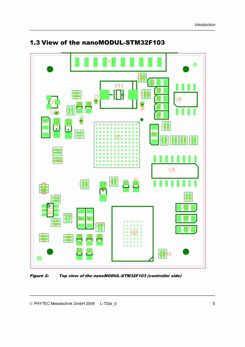
1.3 View of the nanoMODUL-STM32F103
Figure 2: Top view of the nanoMODUL-STM32F103 (controller side)
nanoMODUL-STM32F103
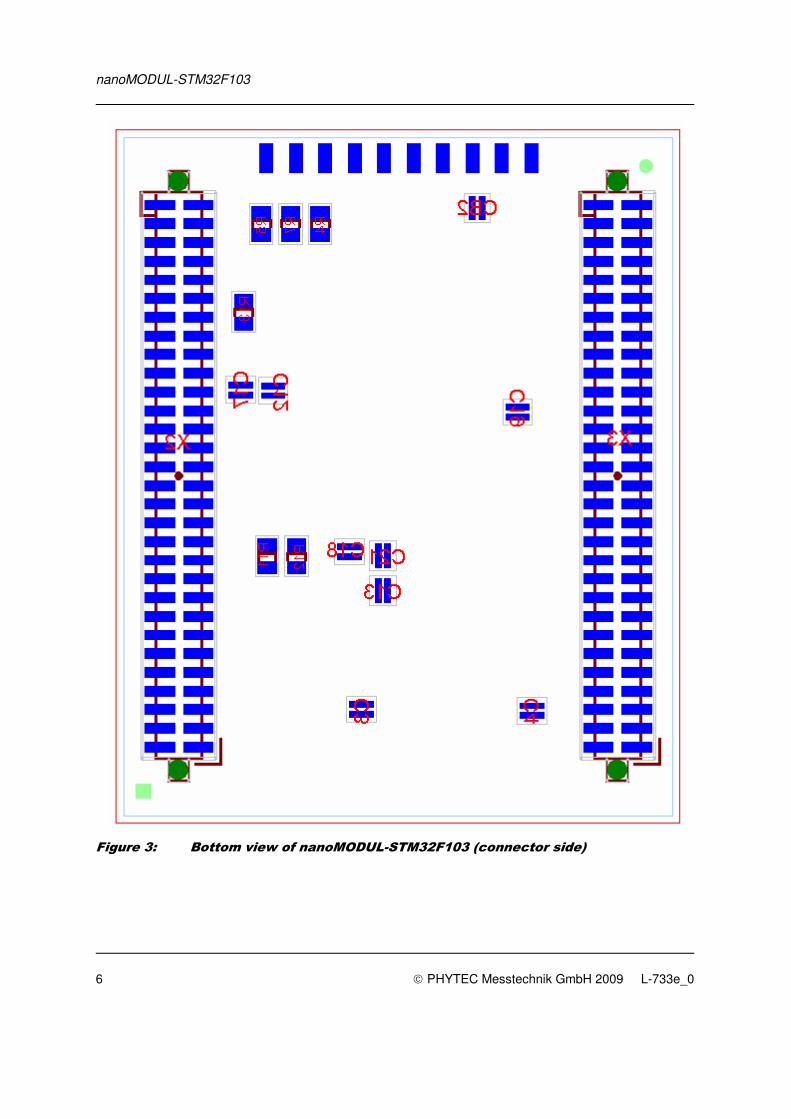
6 PHYTEC Messtechnik GmbH 2009 L-733e_0
Figure 3: Bottom view of nanoMODUL-STM32F103 (connector side)
Jumpers
PHYTEC Messtechnik GmbH 2009 L-733e_0 7
2 Pin Description
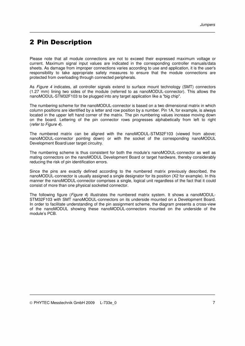
Please note that all module connections are not to exceed their expressed maximum voltage or current. Maximum signal input values are indicated in the corresponding controller manuals/data sheets. As damage from improper connections varies according to use and application, it is the user's responsibility to take appropriate safety measures to ensure that the module connections are protected from overloading through connected peripherals. As Figure 4 indicates, all controller signals extend to surface mount technology (SMT) connectors (1.27 mm) lining two sides of the module (referred to as nanoMODUL-connector). This allows the nanoMODUL-STM32F103 to be plugged into any target application like a "big chip". The numbering scheme for the nanoMODUL-connector is based on a two dimensional matrix in which column positions are identified by a letter and row position by a number. Pin 1A, for example, is always located in the upper left hand corner of the matrix. The pin numbering values increase moving down on the board. Lettering of the pin connector rows progresses alphabetically from left to right (refer to Figure 4). The numbered matrix can be aligned with the nanoMODUL-STM32F103 (viewed from above; nanoMODUL-connector pointing down) or with the socket of the corresponding nanoMODUL Development Board/user target circuitry. The numbering scheme is thus consistent for both the module’s nanoMODUL-connector as well as mating connectors on the nanoMODUL Development Board or target hardware, thereby considerably reducing the risk of pin identification errors. Since the pins are exactly defined according to the numbered matrix previously described, the nanoMODUL-connector is usually assigned a single designator for its position (X2 for example). In this manner the nanoMODUL-connector comprises a single, logical unit regardless of the fact that it could consist of more than one physical socketed connector. The following figure (Figure 4) illustrates the numbered matrix system. It shows a nanoMODUL-STM32F103 with SMT nanoMODUL-connectors on its underside mounted on a Development Board. In order to facilitate understanding of the pin assignment scheme, the diagram presents a cross-view of the nanoMODUL showing these nanoMODUL-connectors mounted on the underside of the module’s PCB.
nanoMODUL-STM32F103
8 PHYTEC Messtechnik GmbH 2009 L-733e_0
Figure 4: Pin-out of the nanoMODUL-Connector
(top view, with cross section insert)
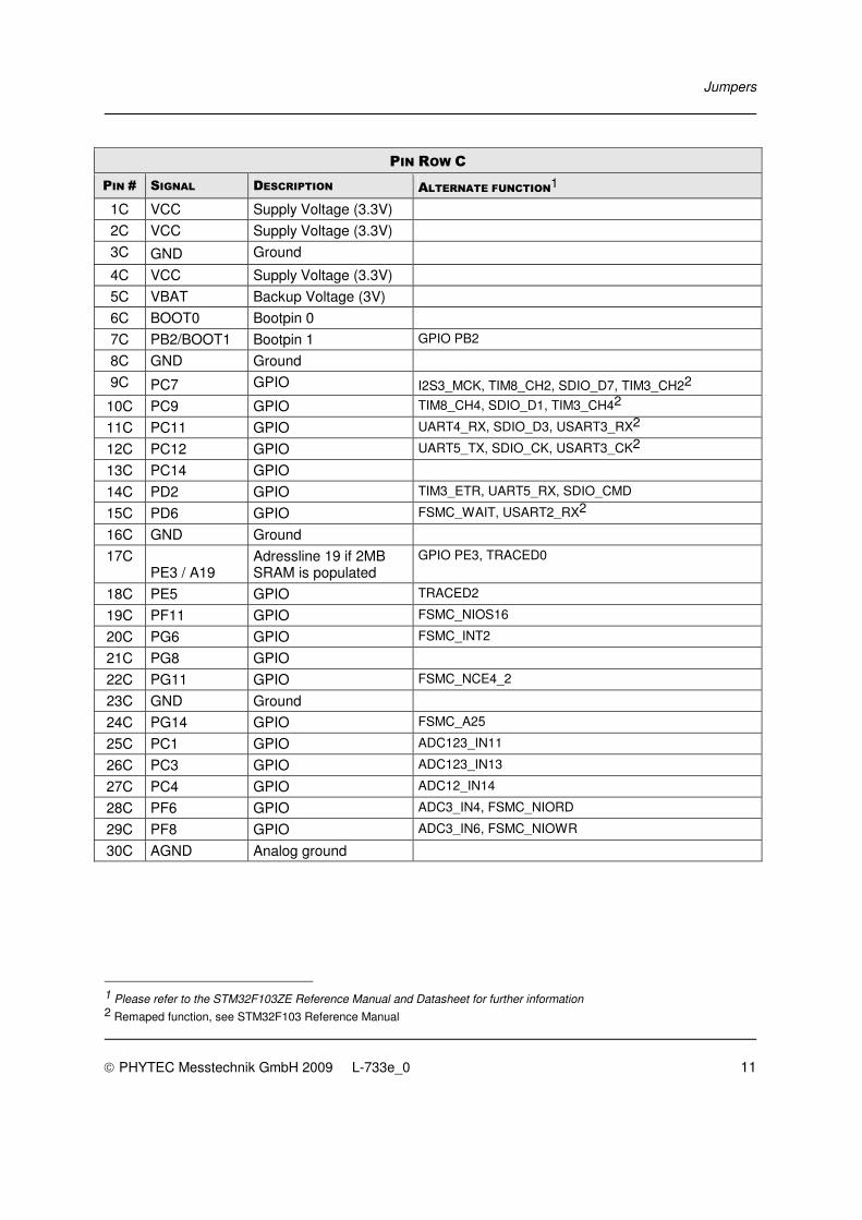
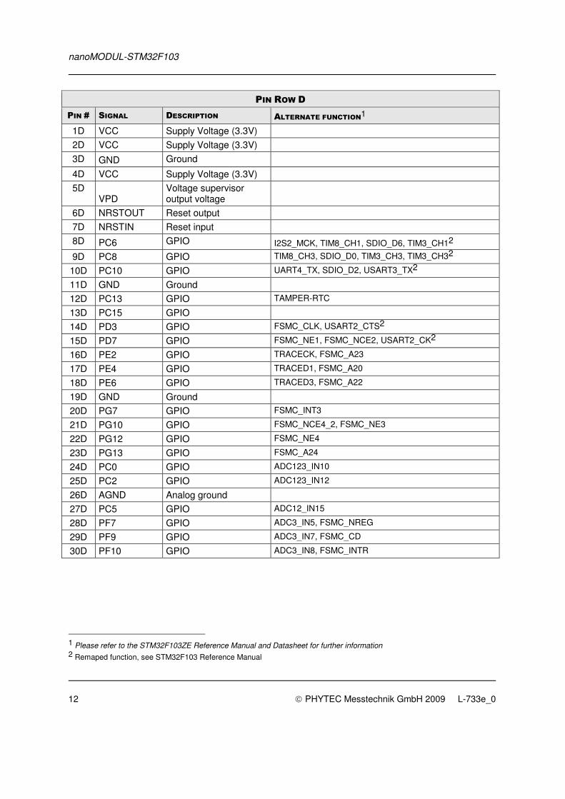
Table 1 provides an overview of the pin-out of the nanoMODUL-connector. Please refer to the STMicroelectronics STM32F103ZE User’s Manual/Data Sheet for details on the functions and features of controller signals and port pins.
Jumpers
PHYTEC Messtechnik GmbH 2009 L-733e_0 9
Table 1: Pin-out of the nanoMODUL-Connector
PIN ROW A
PIN # SIGNAL DESCRIPTION ALTERNATE FUNCTION1
1A PE0 / NBL0 Lower Byte Enable TIM4_ETR
2A PD15 / D1 Databus D1 TIM4_CH42
3A PD1 / D3 Databus D3 CANTX2 above2
4A GND Ground
5A PE9 / D6 Databus D6 TIM1_CH12
6A PE11 / D8 Databus D8 TIM1_CH22
7A PE13 / D10 Databus D10 TIM1_CH32
8A PE14 / D11 Databus D11 TIM1_CH42
9A PD8 / D13 Databus D13 USART3_TX2
10A PD10 / D15 Databus D15 USART3_CK2
11A GND Ground
12A PA2 GPIO USART2_TX, TIM5_CH3, ADC123_IN2, TIM2_CH3
13A PA4 GPIO SPI1_NSS, DAC_OUT1, USART2_CK, ADC12_IN4
14A PA6
GPIO SPI1_MISO, TIM8_BKIN, ADC12_IN6, TIM3_CH1, TIM1_BKIN2
15A PA8 GPIO USART1_CK, TIM1_CH1, MCO
16A R1IN
RS232 Receiver1 Input (UART1)
GPIO PA103, TIM1_CH33
17A R2IN RS232 Receiver2 Input
18A R2OUT RS232 Receiver2 Output
19A GND Ground
20A PA12 GPIO USART1_RTS, CANTX, TIM1_ETR, USBDP
21A JTAG_TCK JTAG Clock GPIO PA14
22A PB0 GPIO ADC12_IN8, TIM3_CH3, TIM8_CH3N, TIM1_CH3N2
23A PB1 GPIO ADC12_IN9, TIM3_CH4, TIM8_CH3N, TIM1_CH3N2
24A JTAG_TRST JTAG Test Reset GPIO PB4, SPI3_MISO, TIM3_CH12,SPI1_MISO2
25A PB6 GPIO I2C_SCL, TIM4_CH1, USART1_TX2
26A GND Ground
27A PB9 GPIO TIM4_CH4, SDIO_D5, I2C1_SDA2, CANTX2
28A PB11 / I2C2_SDA
I²C2 serial data line USART3_RX, TIM2_CH42
29A PB13 GPIO SPI2_SCK, I2S2_CK, USART3_CTS, TIM1_CH1N
30A PB15 GPIO SPI2_MOSI, I2S2_SD, TIM1_CH3N
1 Please refer to the STM32F103ZE Reference Manual and Datasheet for further information 2 Remaped function, see STM32F103 Reference Manual 3 Can be used by setting J10/J11/J12. Refer to section 3
nanoMODUL-STM32F103
10 PHYTEC Messtechnik GmbH 2009 L-733e_0
PIN ROW B
PIN # SIGNAL DESCRIPTION ALTERNATE FUNCTION1
1B PD14 / D0 Databus D0 TIM4_CH32
2B PD0 / D2 Databus D2 CANRX2
3B PE7 / D4 Databus D4 TIM1_ETR2
4B PE8 / D5 Databus D5 TIM1_CH1N2
5B PE10 / D7 Databus D7 TIM1_CH2N2
6B PE12 / D9 Databus D9 TIM1_CH3N2
7B GND Ground
8B PE15 / D12 Databus D12 TIM1_BKIN2
9B PD9 / D14 Databus D14 USART3_RX2
10B PA0
GPIO WKUP, USART2_CTS, ADC123_IN0, TIM2_CH1_ETR,TIM5_CH1, TIM8_ETR
11B PA1 GPIO USART2_RTS, ADC123_IN1, TIM5_CH2, TIM2_CH2
12B PA3 GPIO USART2_RX, TIM5_CH4, ADC123_IN3, TIM2_CH4
13B PA5 GPIO SPI1_SCK, DAC_OUT2, ADC12_IN5
14B PA7
GPIO SPI1_MOSI, TIM8_CH1N, ADC12_IN7, TIM3_CH2, TIM1_CH1N2
15B GND Ground
16B T1OUT
RS232 Transmitter1 Output (UART1)
GPIO PA93,TIM1_CH33
17B T2OUT
RS232 Transmitter2 Output
18B T2IN RS232 Transmitter2 Input
19B PA11 GPIO USART1_CTS, CANRX, TIM1_CH4, USBDM
20B JTAG_TMS JTAG Test Mode Select GPIO PA13
21B JTAG_TDI JTAG Test Data Input GPIO PA15
22B GND Ground
23B JTAG_TDO
JTAG Test Data Output GPIO PB3, TRACESWO, SPI3_SCK, I2S3_CK, TIM2_CH22, SPI1_SCK2
24B PB5
GPIO I2C1_SMBAI, SPI3_MOSI, I2S3_SD, TIM3_CH22,SPI1_MISO
25B PB7 GPIO I2C1_SDA, FSMC_NADV, TIM4_CH2, USART1_RX2
26B PB8 GPIO TIM4_CH3, SDIO_D4, I2C1_SCL2, CANRX2
27B PB10 / I2C2_SCL
I²C2 serial clock line I2C2_SCL, USART3_TX, TIM2_CH32
28B PB12
GPIO SPI2_NSS, I2S2_WS, I2C2_SMBAI, USART3_CK, TIM1_BKIN
29B PB14 GPIO SPI2_MISO, TIM1_CH2N, USART3_RTS
30B GND Ground
1 Please refer to the STM32F103ZE Reference Manual and Datasheet for further information 2 Remaped function, see STM32F103 Reference Manual 3 Can be used by setting J10/J11/J12. Refer to Section 3
Jumpers
PHYTEC Messtechnik GmbH 2009 L-733e_0 11
PIN ROW C
PIN # SIGNAL DESCRIPTION ALTERNATE FUNCTION1
1C VCC Supply Voltage (3.3V)
2C VCC Supply Voltage (3.3V)
3C GND Ground
4C VCC Supply Voltage (3.3V)
5C VBAT Backup Voltage (3V)
6C BOOT0 Bootpin 0
7C PB2/BOOT1 Bootpin 1 GPIO PB2
8C GND Ground
9C PC7 GPIO I2S3_MCK, TIM8_CH2, SDIO_D7, TIM3_CH22
10C PC9 GPIO TIM8_CH4, SDIO_D1, TIM3_CH42
11C PC11 GPIO UART4_RX, SDIO_D3, USART3_RX2
12C PC12 GPIO UART5_TX, SDIO_CK, USART3_CK2
13C PC14 GPIO
14C PD2 GPIO TIM3_ETR, UART5_RX, SDIO_CMD
15C PD6 GPIO FSMC_WAIT, USART2_RX2
16C GND Ground
17C PE3 / A19
Adressline 19 if 2MB SRAM is populated
GPIO PE3, TRACED0
18C PE5 GPIO TRACED2
19C PF11 GPIO FSMC_NIOS16
20C PG6 GPIO FSMC_INT2
21C PG8 GPIO
22C PG11 GPIO FSMC_NCE4_2
23C GND Ground
24C PG14 GPIO FSMC_A25
25C PC1 GPIO ADC123_IN11
26C PC3 GPIO ADC123_IN13
27C PC4 GPIO ADC12_IN14
28C PF6 GPIO ADC3_IN4, FSMC_NIORD
29C PF8 GPIO ADC3_IN6, FSMC_NIOWR
30C AGND Analog ground
1 Please refer to the STM32F103ZE Reference Manual and Datasheet for further information 2 Remaped function, see STM32F103 Reference Manual
nanoMODUL-STM32F103
12 PHYTEC Messtechnik GmbH 2009 L-733e_0
PIN ROW D
PIN # SIGNAL DESCRIPTION ALTERNATE FUNCTION1
1D VCC Supply Voltage (3.3V)
2D VCC Supply Voltage (3.3V)
3D GND Ground
4D VCC Supply Voltage (3.3V)
5D VPD
Voltage supervisor output voltage
6D NRSTOUT Reset output
7D NRSTIN Reset input
8D PC6 GPIO I2S2_MCK, TIM8_CH1, SDIO_D6, TIM3_CH12
9D PC8 GPIO TIM8_CH3, SDIO_D0, TIM3_CH3, TIM3_CH32
10D PC10 GPIO UART4_TX, SDIO_D2, USART3_TX2
11D GND Ground
12D PC13 GPIO TAMPER-RTC
13D PC15 GPIO
14D PD3 GPIO FSMC_CLK, USART2_CTS2
15D PD7 GPIO FSMC_NE1, FSMC_NCE2, USART2_CK2
16D PE2 GPIO TRACECK, FSMC_A23
17D PE4 GPIO TRACED1, FSMC_A20
18D PE6 GPIO TRACED3, FSMC_A22
19D GND Ground
20D PG7 GPIO FSMC_INT3
21D PG10 GPIO FSMC_NCE4_2, FSMC_NE3
22D PG12 GPIO FSMC_NE4
23D PG13 GPIO FSMC_A24
24D PC0 GPIO ADC123_IN10
25D PC2 GPIO ADC123_IN12
26D AGND Analog ground
27D PC5 GPIO ADC12_IN15
28D PF7 GPIO ADC3_IN5, FSMC_NREG
29D PF9 GPIO ADC3_IN7, FSMC_CD
30D PF10 GPIO ADC3_IN8, FSMC_INTR
1 Please refer to the STM32F103ZE Reference Manual and Datasheet for further information 2 Remaped function, see STM32F103 Reference Manual
Jumpers
PHYTEC Messtechnik GmbH 2009 L-733e_0 13
3 Jumpers
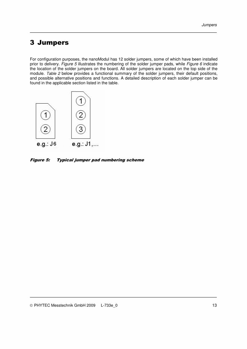
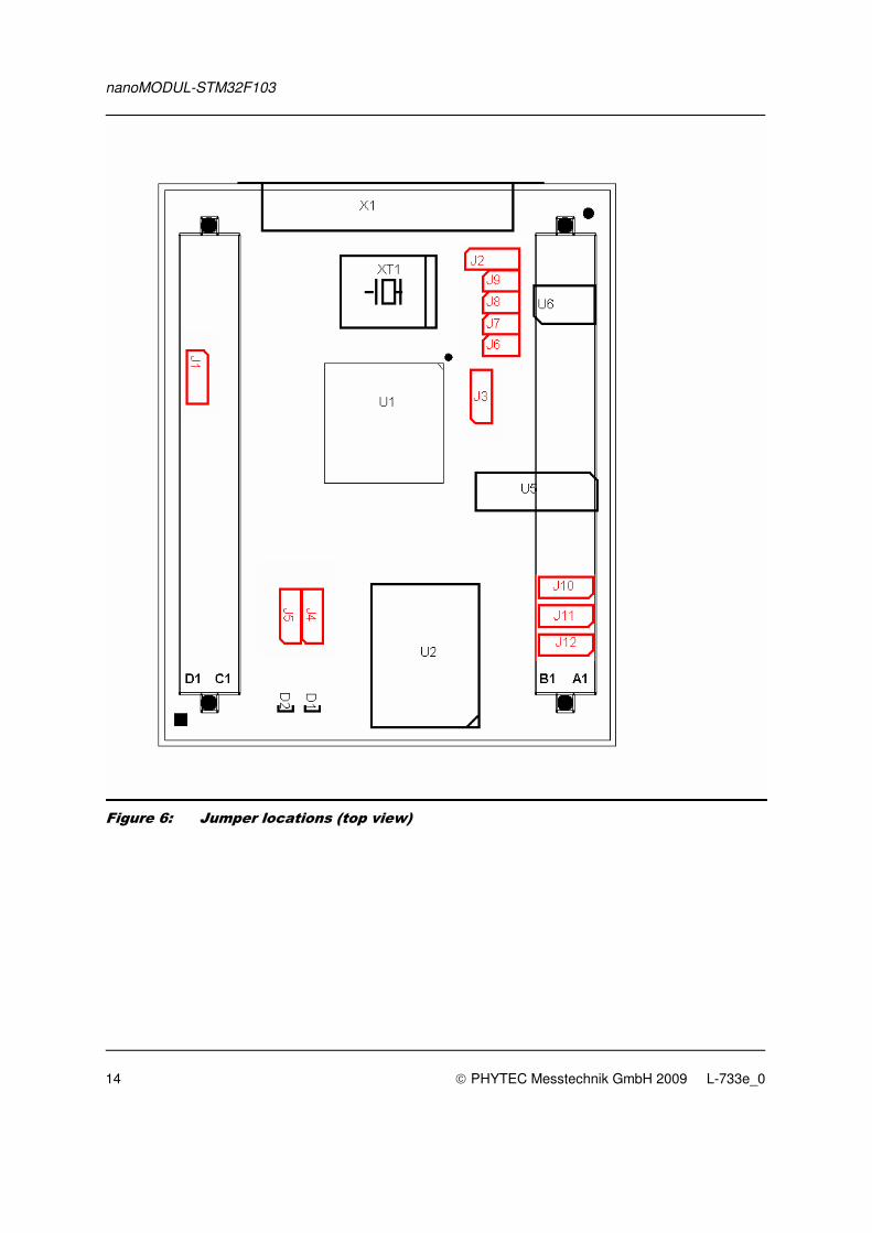
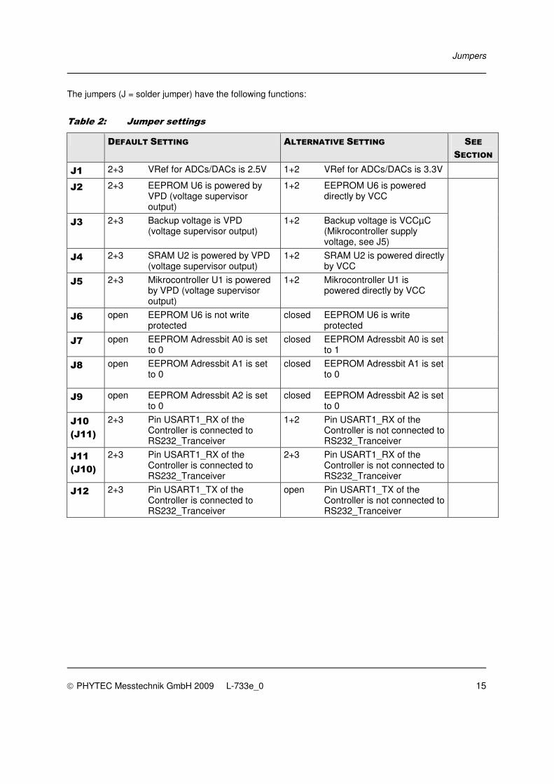
For configuration purposes, the nanoModul has 12 solder jumpers, some of which have been installed prior to delivery. Figure 5 illustrates the numbering of the solder jumper pads, while Figure 6 indicate the location of the solder jumpers on the board. All solder jumpers are located on the top side of the module. Table 2 below provides a functional summary of the solder jumpers, their default positions, and possible alternative positions and functions. A detailed description of each solder jumper can be found in the applicable section listed in the table.
Figure 5: Typical jumper pad numbering scheme
nanoMODUL-STM32F103
14 PHYTEC Messtechnik GmbH 2009 L-733e_0
Figure 6: Jumper locations (top view)
Jumpers
PHYTEC Messtechnik GmbH 2009 L-733e_0 15
The jumpers (J = solder jumper) have the following functions:
Table 2: Jumper settings
DEFAULT SETTING ALTERNATIVE SETTING SEE
SECTION
J1 2+3 VRef for ADCs/DACs is 2.5V 1+2 VRef for ADCs/DACs is 3.3V
J2 2+3 EEPROM U6 is powered by VPD (voltage supervisor output)
1+2 EEPROM U6 is powered directly by VCC
J3 2+3 Backup voltage is VPD (voltage supervisor output)
1+2 Backup voltage is VCCµC (Mikrocontroller supply voltage, see J5)
J4 2+3 SRAM U2 is powered by VPD (voltage supervisor output)
1+2 SRAM U2 is powered directly by VCC
J5 2+3 Mikrocontroller U1 is powered by VPD (voltage supervisor output)
1+2 Mikrocontroller U1 is powered directly by VCC
J6 open EEPROM U6 is not write protected
closed EEPROM U6 is write protected
J7 open EEPROM Adressbit A0 is set to 0
closed EEPROM Adressbit A0 is set to 1
J8 open EEPROM Adressbit A1 is set to 0
closed EEPROM Adressbit A1 is set to 0
J9 open EEPROM Adressbit A2 is set to 0
closed EEPROM Adressbit A2 is set to 0
J10
(J11)
2+3 Pin USART1_RX of the Controller is connected to RS232_Tranceiver
1+2 Pin USART1_RX of the Controller is not connected to RS232_Tranceiver
J11
(J10)
2+3 Pin USART1_RX of the Controller is connected to RS232_Tranceiver
2+3 Pin USART1_RX of the Controller is not connected to RS232_Tranceiver
J12 2+3 Pin USART1_TX of the Controller is connected to RS232_Tranceiver
open Pin USART1_TX of the Controller is not connected to RS232_Tranceiver
nanoMODUL-STM32F103
16 PHYTEC Messtechnik GmbH 2009 L-733e_0
4 Power Requirements
The nanoMODUL-STM32F103 normally operates off of one 3.3V voltage supply denoted as VCC. For Backup purpose there is another voltage input named VBAT.
System Memory
PHYTEC Messtechnik GmbH 2009 L-733e_0 17
5 System Memory
The nanoMODUL provides three types of on-board memory:
• Internal SRAM: 64Kbyte Mikrocontroller internal
• External SRAM: none, 512kByte or 2MByte external
• NAND Flash: 512kByte Mikrocontroller internal
• I²C-EEPROM: 4KB

nanoMODUL-STM32F103
18 PHYTEC Messtechnik GmbH 2009 L-733e_0
5.1 Memory Model
System Memory
PHYTEC Messtechnik GmbH 2009 L-733e_0 19
5.2 External SRAM (U2)
The nanoMODUL-STM32F103 can be optional populated with 512kByte or 2MByte external SRAM. The SRAM is connected to de Controller over the 16-Bit wide databus. FSMC_NE2 (Pin PG9) is used as chip select signal. Thus the address space of the SRAM begins at 0x64000000. If U2 is unpopulated then the databus signals D0-D15, NBL0 (lower byte enable) and the addressbus signal A19 can be used for other purpose e.g. as GPIOs. If 512 kByte SRAM is populated then the addressline A19 can be used for other purpose, too.
nanoMODUL-STM32F103
20 PHYTEC Messtechnik GmbH 2009 L-733e_0
5.3 I²C EEPROM (U6)
The nanoMODUL-STM32F103 is populated with a M24C32WMN6P non-volatile 4KByte EEPROM (U6) with an I²C interface to store configuration data or other general purpose data. This device is accessed through I²C port 2 on the nanoMODUL-STM32F103. The serial clock signal and serial data signal for I²C port 2 are made available at the nanoMODUL-connector as I2C2_SDA on pin 28A and I2C2_SCL on pin 27B. Three solder jumpers are provided to set the lower address bits: J7, J8, and J9. Refer to section 5.3.1 for details on setting these jumpers. Write protection to the device is accomplished via jumper J6. By default this jumper is opened, allowing write access to the EEPROM. Closing this jumper will cause the EEPROM to enter write protect mode, thereby disabling write access to the device. Refer to section 3 for details on setting these jumpers.
System Memory
PHYTEC Messtechnik GmbH 2009 L-733e_0 21
5.3.1 Setting the EEPROM Lower Address Bits (J7, J8, J9)
The 4KB I²C EEPROM populating U6 on the nanoMODUL has the capability of configuring the lower address bits A0, A1, and A2. The four upper address bits of the device are fixed at ‘1010’ (see ST M24C32 data sheet). The remaining three lower address bits of the seven bit I²C device address are configurable using jumpers J7, J8 and J9. J7 sets address bit A0, J8 address bit A1, and J9 address bit A2. Table 3 below shows the resulting seven bit I²C device address for the eight possible jumper configurations.
Table 3: EEPROM I²C address via J7, J8 and J9
U17 I²C DEVICE ADDRESS J6 J5 J4
1010 000 open open open
1010 001 closed open open
1010 010 open closed open
1010 011 closed closed open
1010 100 open open closed
1010 101 closed open closed
1010 110 open closed closed
1010 111 closed closed closed
nanoMODUL-STM32F103
22 PHYTEC Messtechnik GmbH 2009 L-733e_0
5.3.2 EEPROM Write Protection Control (J6)
Jumper J6 controls write access to the EEPROM (U6) device. Opening this jumper allows write access to the device, while closing this jumper enables write protection. The following configurations are possible:
Table 4: EEPROM write protection states via J6
EEPROM WRITE PROTECTION STATE J8
Write access allowed open
Write protected closed
System Memory
PHYTEC Messtechnik GmbH 2009 L-733e_0 23
5.4 RS-232 Transceiver (U5)
One dual RS-232 transceiver supporting 120kbps data rates populates the nanoMODUL-STM32F103 at U5. This device converts the signal levels for:
• USART1_RX (PA10) /USART1_TX (PA9) The RS-232 interface enables connection of the module to a COM port on a host-PC. In this instance the Rx line of the transceiver is connected to the Tx line of the COM port; while the Tx line of the transceiver is connected to the Rx line of the COM port. The ground potential of the nanoMODUL-STM32F103 circuitry needs to be connected to the applicable ground pin on the COM port as well. The nanoMODUL-STM32F103 does not convert the remaining USARTs/UARTs (USART2, USART3, UART4, UART5) provided by the STM32F103ZE to RS-232 levels. The TTL level signals are made available at the nanoMODUL-connector. External RS-232 transceivers must be supplied by the user if additional UART’s require RS-232 levels or the second transceiver of the dual RS-232 trainsceiver-IC can be used. With the RS-232 Transceiver, UART1 can be used to program the internal Flash of the Mikrocontroller via the internal Bootloader. The pins of the second RS-232 Transceiver are made available at the nanoMODUL-connector so that they can be used by external signals.

nanoMODUL-STM32F103
24 PHYTEC Messtechnik GmbH 2009 L-733e_0
JTAG Interface
PHYTEC Messtechnik GmbH 2009 L-733e_0 25
6 JTAG Interface (X1)
The nanoMODUL-STM32F103 is equipped with a JTAG interface for downloading program code into the internal flash, internal RAM or for debugging programs currently executing. The JTAG interface extends out to a 2.0 mm pitch pin header at X1 on the edge of the module PCB. All JTAG signals are also made available on the nanoMODUL-connector.
nanoMODUL-STM32F103
26 PHYTEC Messtechnik GmbH 2009 L-733e_0
7 Technical Specifications
Additional specifications (all TBD):
• Dimensions: 38.3mm x 47.1mm
• Storage temperature: -40°C to +125°C
• Operating temperature: -40°C to +85°C (industrial)
• Operating voltage: VCC 2.9V to 3.6V VBAT TBD to TBDV
• Power consumption: 60mA typical
Conditions: VCC = 3.3 V ,VBAT = 0 V, 2 MByte external SRAM,
nanoMODUL-STM32F103 Baseboard
PHYTEC Messtechnik GmbH 2009 L-733e_0 27
8 nanoMODUL-STM32F103 Baseboard
nanoMODUL-STM32F103 Baseboard Technical Highlights
• Up to 12 digital inputs, 24VDC, galvanically isolated
• 6 switchable relay outputs, 250VAC, 2A
• Up to 8 high side switches, 24VDC, up to 1,9A, short circuit proof, galvanically isolated
• Up to 8 analog inputs, 0-10VDC, 12-bit
• 2 analog outputs, 0-10V, 8- or 12-bit
• USB
• CAN
• RS232
• Connector with a lot of different functions (Timer, ADC, GPIO, I²C, SPI) for different purpose such as motor driver
• Operating Voltage: 24VDC for low power domain, 24VDC for high side switches
• Board can be powered over USB for prototyping with some restrictions
nanoMODUL-STM32F103
28 PHYTEC Messtechnik GmbH 2009 L-733e_0
Index
PHYTEC Messtechnik GmbH 2009 L-733e_0 29
Index
B
Block Diagram ............................... 4
C
COM Port..................................... 23
D
Debug Interface........................... 24 Dimensions.................................. 25
E
EEPROM............................... 17, 20 EEPROM Write Protection .......... 22
F
Features ..................................... 3
I
I²C EEPROM ............................... 20
J
J603............................................. 22 JTAG Interface ............................ 24
N
NAND Flash................................. 17
O
Operating Temperature ............... 25 Operating Voltage........................ 25
P
phyCORE-connector..................7, 8 Pin Description...............................7 Pinout.............................................9 Power Consumption ....................25
R
RS-232 Interface..........................23 RS-232 Level ...............................23 RS-232 Transceiver.....................23
S
SMT Connector..............................7 Storage Temperature...................25 System Memory...........................17
T
Technical Specifications ........25, 28 TTL Level.....................................23
U
U301 ............................................23 U302 ............................................23 U601 ......................................19, 20 UART3.........................................23 UART5.........................................23
X
X201 ............................................24

nanoMODUL-STM32F103
30 PHYTEC Messtechnik GmbH 2009 L-733e_0

Suggestions for Improvement
PHYTEC MesstechnikGmbH 2009 L-733e_0
Document: nanoMODUL-STM32F103 Document number: L-733e_0, Preliminary Version, April 2009 How would you improve this manual?
Did you find any mistakes in this manual? page
Submitted by: Customer number:
Name:
Company:
Address:
Return to: PHYTEC Technologie Holding AG Postfach 100403 D-55135 Mainz, Germany Fax : +49 (6131) 9221-33

Published by
PHYTEC Messtechnik GmbH 2009 Ordering No. L-733e_0
Printed in Germany