Embed Size (px)
Citation preview

FP3/FP10SH HardwareARCT1F300E-1 06.9
FP3/FP10SHHardware
PROGRAMMABLE CONTROLLER

Safety Precautions Observe the following notices to ensure personal safety or to prevent accidents. To ensure that you use this product correctly, read this User’s Manual thoroughly before use. Make sure that you fully understand the product and information on safe. This manual uses two safety flags to indicate different levels of danger. WARNING If critical situations that could lead to user’s death or serious injury is assumed by mishandling of the product. -Always take precautions to ensure the overall safety of your system, so that the whole system remains safe in the event of failure of this product or other external factor.
-Do not use this product in areas with inflammable gas. It could lead to an explosion. -Exposing this product to excessive heat or open flames could cause damage to the lithium battery or other electronic parts.
CAUTION If critical situations that could lead to user’s injury or only property damage is assumed by mishandling of the product. -To prevent abnormal exothermic heat or smoke generation, use this product at the values less than the maximum of the characteristics and performance that are assure in these specifications.
-Do not dismantle or remodel the product. It could lead to abnormal exothermic heat or smoke generation.
-Do not touch the terminal while turning on electricity. It could lead to an electric shock.. -Use the external devices to function the emergency stop and interlock circuit. -Connect the wires or connectors securely. The loose connection might cause abnormal exothermic heat or smoke generation
-Do not allow foreign matters such as liquid, flammable materials, metals to go into the inside of the product. It might cause exothermic heat or smoke generation. -Do not undertake construction (such as connection and disconnection) while the power supply is on.
Copyright / Trademarks -This manual and its contents are copylighted. -You may not copy this manual,in whole or part,without written consent of Matsushita Electric Works,Ltd.
-Windows and Windows NT are registered trademarks of Microsoft Corporation in the United States and/or other countries. -All other company names and product names are trademarks or registered trademarks of their respective owners. -Matsushita Electric Works,Ltd. pursues a policy of continuous improvement of the Design and performan e of its products, therefore,we reserve the right to change the manual/ cproduct without notice.


Table of Contents FP3/FP10SH
ii Matsushita Automation Controls
Table of Contents
Before You Start x. . . . . . . . . . . . . . . . . . . . . . . . . . . . . . . . . . . . . . . . . . . . .
Chapter 1 Features and System Configuration
1.1 General Features 1 − 3. . . . . . . . . . . . . . . . . . . . . . . . . . . . . . . . . . . . . . . . . . . . . . . .1.2 Basic System Configuration 1 − 6. . . . . . . . . . . . . . . . . . . . . . . . . . . . . . . . . . . . . . .
1.2.1 Basic Configuration and Number of Control I/O Points 1 − 6. . . . . . . .1.2.2 Configuration and Number of Control I/O Points When
Expanded 1 − 8. . . . . . . . . . . . . . . . . . . . . . . . . . . . . . . . . . . . . . . . . . . . . .1.3 Unit Combinations 1 − 10. . . . . . . . . . . . . . . . . . . . . . . . . . . . . . . . . . . . . . . . . . . . . .
1.3.1 Unit Line−Up 1 − 10. . . . . . . . . . . . . . . . . . . . . . . . . . . . . . . . . . . . . . . . . . .1.3.2 Restrictions on Unit Types 1 − 12. . . . . . . . . . . . . . . . . . . . . . . . . . . . . . .1.3.3 Limitations on Current Consumption 1 − 15. . . . . . . . . . . . . . . . . . . . . .
1.4 Expansion System Configuration 1 − 20. . . . . . . . . . . . . . . . . . . . . . . . . . . . . . . . .1.4.1 MEWNET−F (remote I/O) Configuration 1 − 20. . . . . . . . . . . . . . . . . . .1.4.2 MEWNET−TR System Configuration 1 − 22. . . . . . . . . . . . . . . . . . . . . .1.4.3 MEWNET−W System Configuration 1 − 24. . . . . . . . . . . . . . . . . . . . . . .1.4.4 MEWNET−P Configuration 1 − 26. . . . . . . . . . . . . . . . . . . . . . . . . . . . . .1.4.5 Computer Link Function 1 − 28. . . . . . . . . . . . . . . . . . . . . . . . . . . . . . . . .1.4.6 Control by MODEM 1 − 30. . . . . . . . . . . . . . . . . . . . . . . . . . . . . . . . . . . . .
1.5 Programming Tools 1 − 32. . . . . . . . . . . . . . . . . . . . . . . . . . . . . . . . . . . . . . . . . . . . .1.5.1 Tools Needed for Programming 1 − 32. . . . . . . . . . . . . . . . . . . . . . . . . . .
1.5.1.1 Using NPST−GR Software for FP3 1 − 32. . . . . . . . . . . . . .1.5.1.2 Using NPST−GR Software for FP10SH 1 − 33. . . . . . . . . .1.5.1.3 Using FP Programmer II Ver.2 for FP3 Only 1 − 33. . . . . .
1.5.2 Table of Programming Tools 1 − 34. . . . . . . . . . . . . . . . . . . . . . . . . . . . . .1.5.3 Tools Needed for ROM Writing of FP3 1 − 35. . . . . . . . . . . . . . . . . . . . .
1.5.3.1 When Creating a ROM With a CommerciallyAvailable ROM Writer, Through a MasterMemory (EEPROM) 1 − 35. . . . . . . . . . . . . . . . . . . . . . . . . . .
1.5.3.2 When Creating a ROM With NPST−GR Softwareand a Commercially Available ROM Writer 1 − 36. . . . . . .
1.5.4 Tools Needed for ROM Writing of FP10SH 1 − 37. . . . . . . . . . . . . . . . .1.5.4.1 When Creating a ROM With a Commercially
Available ROM Writer, Through a MasterMemory (FROM) 1 − 37. . . . . . . . . . . . . . . . . . . . . . . . . . . . . .
1.5.4.2 When Creating a ROM With NPST−GR Softwareand a Commercially Available ROM Writer 1 − 38. . . . . . .
Chapter 2 Parts and Its Specifications
2.1 Specifications 2 − 3. . . . . . . . . . . . . . . . . . . . . . . . . . . . . . . . . . . . . . . . . . . . . . . . . . .2.1.1 FP3/FP10SH General Specifications 2 − 3. . . . . . . . . . . . . . . . . . . . . . .2.1.2 Dimensions 2 − 3. . . . . . . . . . . . . . . . . . . . . . . . . . . . . . . . . . . . . . . . . . . . .2.1.3 FP3 Performance Specifications 2 − 4. . . . . . . . . . . . . . . . . . . . . . . . . . .
Table of ContentsFP3/FP10SH
iiiMatsushita Automation Controls
2.1.4 FP10SH Performance Specifications 2 − 7. . . . . . . . . . . . . . . . . . . . . . .2.2 Backplane for FP3/FP10SH 2 − 10. . . . . . . . . . . . . . . . . . . . . . . . . . . . . . . . . . . . . .2.3 Expansion Cable 2 − 12. . . . . . . . . . . . . . . . . . . . . . . . . . . . . . . . . . . . . . . . . . . . . . .2.4 FP3 CPU and Optional Memory 2 − 14. . . . . . . . . . . . . . . . . . . . . . . . . . . . . . . . . .
2.4.1 FP3 CPU 2 − 14. . . . . . . . . . . . . . . . . . . . . . . . . . . . . . . . . . . . . . . . . . . . . .2.4.1.1 Status Indicator LEDs 2 − 16. . . . . . . . . . . . . . . . . . . . . . . . .2.4.1.2 Initialize/Test Switch 2 − 17. . . . . . . . . . . . . . . . . . . . . . . . . . .2.4.1.3 Mode Selector 2 − 17. . . . . . . . . . . . . . . . . . . . . . . . . . . . . . . .
2.4.2 Memory (EPROM) and Master Memory (EEPROM) 2 − 18. . . . . . . . .2.5 FP10SH CPU and Optional Memory 2 − 20. . . . . . . . . . . . . . . . . . . . . . . . . . . . . .
2.5.1 FP10SH CPU 2 − 20. . . . . . . . . . . . . . . . . . . . . . . . . . . . . . . . . . . . . . . . . .2.5.1.1 Status Indicator LEDs 2 − 22. . . . . . . . . . . . . . . . . . . . . . . . .2.5.1.2 Initialize/Test Switch 2 − 23. . . . . . . . . . . . . . . . . . . . . . . . . . .2.5.1.3 Mode Selector 2 − 23. . . . . . . . . . . . . . . . . . . . . . . . . . . . . . . .2.5.1.4 Operation Condition Switches 2 − 24. . . . . . . . . . . . . . . . . .2.5.1.5 Station Number Setting Switches 2 − 26. . . . . . . . . . . . . . . .2.5.1.6 COM Port (RS232C) 2 − 26. . . . . . . . . . . . . . . . . . . . . . . . . .
2.5.2 Expansion Memory Unit 2 − 29. . . . . . . . . . . . . . . . . . . . . . . . . . . . . . . . .2.5.3 ROM Operation Board 2 − 31. . . . . . . . . . . . . . . . . . . . . . . . . . . . . . . . . .2.5.4 IC Memory Card Board 2 − 35. . . . . . . . . . . . . . . . . . . . . . . . . . . . . . . . . .2.5.5 IC Memory Card 2 − 37. . . . . . . . . . . . . . . . . . . . . . . . . . . . . . . . . . . . . . . .
2.6 Power Supply Units 2 − 42. . . . . . . . . . . . . . . . . . . . . . . . . . . . . . . . . . . . . . . . . . . . .2.6.1 Power Supply Specifications 2 − 44. . . . . . . . . . . . . . . . . . . . . . . . . . . . .
2.7 Power Supply Dummy Unit 2 − 45. . . . . . . . . . . . . . . . . . . . . . . . . . . . . . . . . . . . . .2.7.1 Conditions for Using a Power Supply Dummy Unit 2 − 46. . . . . . . . . .2.7.2 Installing the Power Supply Dummy Unit 2 − 48. . . . . . . . . . . . . . . . . . .
2.8 Common Specifications of Input, Output and I/O Mixed Units 2 − 49. . . . . . . . .2.8.1 Table of Input Unit Types 2 − 50. . . . . . . . . . . . . . . . . . . . . . . . . . . . . . . .2.8.2 Table of Output Unit Types 2 − 50. . . . . . . . . . . . . . . . . . . . . . . . . . . . . . .2.8.3 Table of I/O Mixed Unit Types 2 − 51. . . . . . . . . . . . . . . . . . . . . . . . . . . .
2.9 Input Units Specifications 2 − 52. . . . . . . . . . . . . . . . . . . . . . . . . . . . . . . . . . . . . . . .2.9.1 16-point Type DC Input Unit 2 − 52. . . . . . . . . . . . . . . . . . . . . . . . . . . . . .
2.9.1.1 Specifications 2 − 52. . . . . . . . . . . . . . . . . . . . . . . . . . . . . . . .2.9.1.2 Internal Circuit Diagram 2 − 53. . . . . . . . . . . . . . . . . . . . . . . .2.9.1.3 Pin Layout of Terminal Block 2 − 53. . . . . . . . . . . . . . . . . . . .
2.9.2 32-point Type DC Input Units 2 − 54. . . . . . . . . . . . . . . . . . . . . . . . . . . . .2.9.2.1 Specifications 2 − 54. . . . . . . . . . . . . . . . . . . . . . . . . . . . . . . .2.9.2.2 Internal Circuit Diagram 2 − 55. . . . . . . . . . . . . . . . . . . . . . . .2.9.2.3 Pin Layout of Connector 2 − 56. . . . . . . . . . . . . . . . . . . . . . .
2.9.3 64-point Type DC Input Units 2 − 57. . . . . . . . . . . . . . . . . . . . . . . . . . . . .2.9.3.1 Specifications 2 − 57. . . . . . . . . . . . . . . . . . . . . . . . . . . . . . . .2.9.3.2 Internal Circuit Diagram 2 − 57. . . . . . . . . . . . . . . . . . . . . . . .2.9.3.3 Pin Layout of Connector 2 − 58. . . . . . . . . . . . . . . . . . . . . . .2.9.3.4 Internal Current Consumption Switch 2 − 59. . . . . . . . . . . .2.9.3.5 Limitations on Number of Simultaneous Input ON
Points 2 − 60. . . . . . . . . . . . . . . . . . . . . . . . . . . . . . . . . . . . . . .2.9.3.6 Notes Regarding the Internal Current Consumption
Switch Settings 2 − 60. . . . . . . . . . . . . . . . . . . . . . . . . . . . . . .2.9.4 64-point/High−speed Response Type DC Input Units 2 − 61. . . . . . . .
Table of Contents FP3/FP10SH
iv Matsushita Automation Controls
2.9.4.1 Specifications 2 − 61. . . . . . . . . . . . . . . . . . . . . . . . . . . . . . . .2.9.4.2 Internal Circuit Diagram 2 − 61. . . . . . . . . . . . . . . . . . . . . . . .2.9.4.3 Pin Layout of Connector 2 − 62. . . . . . . . . . . . . . . . . . . . . . .2.9.4.4 Limitations on Number of Simultaneous Input ON
Points 2 − 63. . . . . . . . . . . . . . . . . . . . . . . . . . . . . . . . . . . . . . .2.9.5 8-point Type AC Input Units 2 − 64. . . . . . . . . . . . . . . . . . . . . . . . . . . . . .
2.9.5.1 Specifications 2 − 64. . . . . . . . . . . . . . . . . . . . . . . . . . . . . . . .2.9.5.2 Internal Circuit Diagram 2 − 65. . . . . . . . . . . . . . . . . . . . . . . .2.9.5.3 Pin Layout of Terminal Block 2 − 65. . . . . . . . . . . . . . . . . . . .
2.9.6 16-point Type AC Input Units 2 − 66. . . . . . . . . . . . . . . . . . . . . . . . . . . . .2.9.6.1 Specifications 2 − 66. . . . . . . . . . . . . . . . . . . . . . . . . . . . . . . .2.9.6.2 Internal Circuit Diagram 2 − 67. . . . . . . . . . . . . . . . . . . . . . . .2.9.6.3 Pin Layout of Terminal Block 2 − 67. . . . . . . . . . . . . . . . . . . .
2.10 Output Units Specifications 2 − 68. . . . . . . . . . . . . . . . . . . . . . . . . . . . . . . . . . . . . .2.10.1 16-point Type Relay Output Units 2 − 68. . . . . . . . . . . . . . . . . . . . . . . . .
2.10.1.1 Specifications 2 − 68. . . . . . . . . . . . . . . . . . . . . . . . . . . . . . . .2.10.1.2 Internal Circuit Diagram 2 − 69. . . . . . . . . . . . . . . . . . . . . . . .2.10.1.3 Pin Layout of Terminal Block 2 − 69. . . . . . . . . . . . . . . . . . . .
2.10.2 16-point Type Output Unit−Transistor NPN 2 − 70. . . . . . . . . . . . . . . . .2.10.2.1 Specifications 2 − 70. . . . . . . . . . . . . . . . . . . . . . . . . . . . . . . .2.10.2.2 Internal Circuit Diagram 2 − 71. . . . . . . . . . . . . . . . . . . . . . . .2.10.2.3 Pin Layout of Terminal Block 2 − 71. . . . . . . . . . . . . . . . . . . .
2.10.3 32-point Type Output Unit−Transistor NPN 2 − 72. . . . . . . . . . . . . . . . .2.10.3.1 Specifications 2 − 72. . . . . . . . . . . . . . . . . . . . . . . . . . . . . . . .2.10.3.2 Internal Circuit Diagram 2 − 73. . . . . . . . . . . . . . . . . . . . . . . .2.10.3.3 Pin Layout of Connector 2 − 73. . . . . . . . . . . . . . . . . . . . . . .
2.10.4 64-point Type Output Unit−Transistor NPN 2 − 74. . . . . . . . . . . . . . . . .2.10.4.1 Specifications 2 − 74. . . . . . . . . . . . . . . . . . . . . . . . . . . . . . . .2.10.4.2 Internal Circuit Diagram 2 − 75. . . . . . . . . . . . . . . . . . . . . . . .2.10.4.3 Pin Layout of Connector 2 − 75. . . . . . . . . . . . . . . . . . . . . . .
2.10.5 16-point Type Output Unit−Transistor PNP 2 − 76. . . . . . . . . . . . . . . . .2.10.5.1 Specifications 2 − 76. . . . . . . . . . . . . . . . . . . . . . . . . . . . . . . .2.10.5.2 Internal Circuit Diagram 2 − 77. . . . . . . . . . . . . . . . . . . . . . . .2.10.5.3 Pin Layout of Terminal Block 2 − 77. . . . . . . . . . . . . . . . . . . .
2.10.6 32-point type Output Unit−Transistor PNP 2 − 78. . . . . . . . . . . . . . . . . .2.10.6.1 Specifications 2 − 78. . . . . . . . . . . . . . . . . . . . . . . . . . . . . . . .2.10.6.2 Internal Circuit Diagram 2 − 79. . . . . . . . . . . . . . . . . . . . . . . .2.10.6.3 Pin Layout of Connector 2 − 79. . . . . . . . . . . . . . . . . . . . . . .
2.10.7 64-point Type Output Unit−Transistor PNP 2 − 80. . . . . . . . . . . . . . . . .2.10.7.1 Specifications 2 − 80. . . . . . . . . . . . . . . . . . . . . . . . . . . . . . . .2.10.7.2 Internal Circuit Diagram 2 − 81. . . . . . . . . . . . . . . . . . . . . . . .2.10.7.3 Pin Layout of Connector 2 − 81. . . . . . . . . . . . . . . . . . . . . . .
2.10.8 16-point Type Triac Output Unit 2 − 82. . . . . . . . . . . . . . . . . . . . . . . . . . .2.10.8.1 Specifications 2 − 82. . . . . . . . . . . . . . . . . . . . . . . . . . . . . . . .2.10.8.2 Internal Circuit Diagram 2 − 83. . . . . . . . . . . . . . . . . . . . . . . .2.10.8.3 Pin Layout of Terminal Block 2 − 83. . . . . . . . . . . . . . . . . . . .
2.11 I/O Mixed Units Specifications 2 − 84. . . . . . . . . . . . . . . . . . . . . . . . . . . . . . . . . . . .2.11.1 64−point Type I/O Mixed Unit−DC Input/Transistor NPN 2 − 84. . . . .
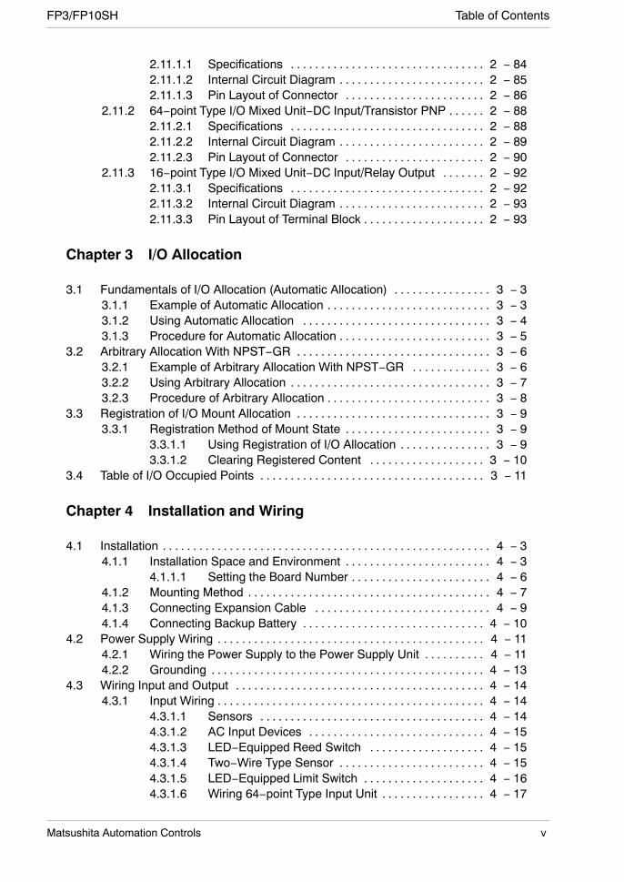
Table of ContentsFP3/FP10SH
vMatsushita Automation Controls
2.11.1.1 Specifications 2 − 84. . . . . . . . . . . . . . . . . . . . . . . . . . . . . . . .2.11.1.2 Internal Circuit Diagram 2 − 85. . . . . . . . . . . . . . . . . . . . . . . .2.11.1.3 Pin Layout of Connector 2 − 86. . . . . . . . . . . . . . . . . . . . . . .
2.11.2 64−point Type I/O Mixed Unit−DC Input/Transistor PNP 2 − 88. . . . . .2.11.2.1 Specifications 2 − 88. . . . . . . . . . . . . . . . . . . . . . . . . . . . . . . .2.11.2.2 Internal Circuit Diagram 2 − 89. . . . . . . . . . . . . . . . . . . . . . . .2.11.2.3 Pin Layout of Connector 2 − 90. . . . . . . . . . . . . . . . . . . . . . .
2.11.3 16−point Type I/O Mixed Unit−DC Input/Relay Output 2 − 92. . . . . . .2.11.3.1 Specifications 2 − 92. . . . . . . . . . . . . . . . . . . . . . . . . . . . . . . .2.11.3.2 Internal Circuit Diagram 2 − 93. . . . . . . . . . . . . . . . . . . . . . . .2.11.3.3 Pin Layout of Terminal Block 2 − 93. . . . . . . . . . . . . . . . . . . .
Chapter 3 I/O Allocation
3.1 Fundamentals of I/O Allocation (Automatic Allocation) 3 − 3. . . . . . . . . . . . . . . .3.1.1 Example of Automatic Allocation 3 − 3. . . . . . . . . . . . . . . . . . . . . . . . . . .3.1.2 Using Automatic Allocation 3 − 4. . . . . . . . . . . . . . . . . . . . . . . . . . . . . . .3.1.3 Procedure for Automatic Allocation 3 − 5. . . . . . . . . . . . . . . . . . . . . . . . .
3.2 Arbitrary Allocation With NPST−GR 3 − 6. . . . . . . . . . . . . . . . . . . . . . . . . . . . . . . .3.2.1 Example of Arbitrary Allocation With NPST−GR 3 − 6. . . . . . . . . . . . .3.2.2 Using Arbitrary Allocation 3 − 7. . . . . . . . . . . . . . . . . . . . . . . . . . . . . . . . .3.2.3 Procedure of Arbitrary Allocation 3 − 8. . . . . . . . . . . . . . . . . . . . . . . . . . .
3.3 Registration of I/O Mount Allocation 3 − 9. . . . . . . . . . . . . . . . . . . . . . . . . . . . . . . .3.3.1 Registration Method of Mount State 3 − 9. . . . . . . . . . . . . . . . . . . . . . . .
3.3.1.1 Using Registration of I/O Allocation 3 − 9. . . . . . . . . . . . . . .3.3.1.2 Clearing Registered Content 3 − 10. . . . . . . . . . . . . . . . . . .
3.4 Table of I/O Occupied Points 3 − 11. . . . . . . . . . . . . . . . . . . . . . . . . . . . . . . . . . . . .
Chapter 4 Installation and Wiring
4.1 Installation 4 − 3. . . . . . . . . . . . . . . . . . . . . . . . . . . . . . . . . . . . . . . . . . . . . . . . . . . . . .4.1.1 Installation Space and Environment 4 − 3. . . . . . . . . . . . . . . . . . . . . . . .
4.1.1.1 Setting the Board Number 4 − 6. . . . . . . . . . . . . . . . . . . . . . .4.1.2 Mounting Method 4 − 7. . . . . . . . . . . . . . . . . . . . . . . . . . . . . . . . . . . . . . . .4.1.3 Connecting Expansion Cable 4 − 9. . . . . . . . . . . . . . . . . . . . . . . . . . . . .4.1.4 Connecting Backup Battery 4 − 10. . . . . . . . . . . . . . . . . . . . . . . . . . . . . .
4.2 Power Supply Wiring 4 − 11. . . . . . . . . . . . . . . . . . . . . . . . . . . . . . . . . . . . . . . . . . . .4.2.1 Wiring the Power Supply to the Power Supply Unit 4 − 11. . . . . . . . . .4.2.2 Grounding 4 − 13. . . . . . . . . . . . . . . . . . . . . . . . . . . . . . . . . . . . . . . . . . . . .
4.3 Wiring Input and Output 4 − 14. . . . . . . . . . . . . . . . . . . . . . . . . . . . . . . . . . . . . . . . .4.3.1 Input Wiring 4 − 14. . . . . . . . . . . . . . . . . . . . . . . . . . . . . . . . . . . . . . . . . . . .
4.3.1.1 Sensors 4 − 14. . . . . . . . . . . . . . . . . . . . . . . . . . . . . . . . . . . . .4.3.1.2 AC Input Devices 4 − 15. . . . . . . . . . . . . . . . . . . . . . . . . . . . .4.3.1.3 LED−Equipped Reed Switch 4 − 15. . . . . . . . . . . . . . . . . . .4.3.1.4 Two−Wire Type Sensor 4 − 15. . . . . . . . . . . . . . . . . . . . . . . .4.3.1.5 LED−Equipped Limit Switch 4 − 16. . . . . . . . . . . . . . . . . . . .4.3.1.6 Wiring 64−point Type Input Unit 4 − 17. . . . . . . . . . . . . . . . .
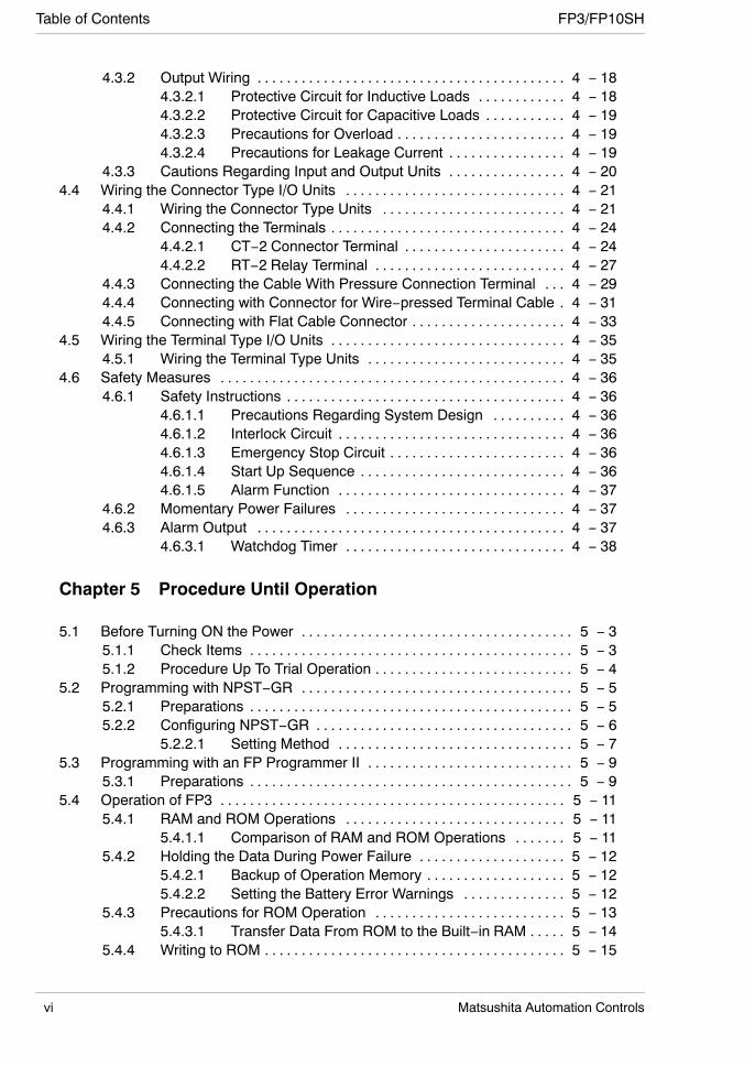
Table of Contents FP3/FP10SH
vi Matsushita Automation Controls
4.3.2 Output Wiring 4 − 18. . . . . . . . . . . . . . . . . . . . . . . . . . . . . . . . . . . . . . . . . .4.3.2.1 Protective Circuit for Inductive Loads 4 − 18. . . . . . . . . . . .4.3.2.2 Protective Circuit for Capacitive Loads 4 − 19. . . . . . . . . . .4.3.2.3 Precautions for Overload 4 − 19. . . . . . . . . . . . . . . . . . . . . . .4.3.2.4 Precautions for Leakage Current 4 − 19. . . . . . . . . . . . . . . .
4.3.3 Cautions Regarding Input and Output Units 4 − 20. . . . . . . . . . . . . . . .4.4 Wiring the Connector Type I/O Units 4 − 21. . . . . . . . . . . . . . . . . . . . . . . . . . . . . .
4.4.1 Wiring the Connector Type Units 4 − 21. . . . . . . . . . . . . . . . . . . . . . . . .4.4.2 Connecting the Terminals 4 − 24. . . . . . . . . . . . . . . . . . . . . . . . . . . . . . . .
4.4.2.1 CT−2 Connector Terminal 4 − 24. . . . . . . . . . . . . . . . . . . . . .4.4.2.2 RT−2 Relay Terminal 4 − 27. . . . . . . . . . . . . . . . . . . . . . . . . .
4.4.3 Connecting the Cable With Pressure Connection Terminal 4 − 29. . .4.4.4 Connecting with Connector for Wire−pressed Terminal Cable 4 − 31.4.4.5 Connecting with Flat Cable Connector 4 − 33. . . . . . . . . . . . . . . . . . . . .
4.5 Wiring the Terminal Type I/O Units 4 − 35. . . . . . . . . . . . . . . . . . . . . . . . . . . . . . . .4.5.1 Wiring the Terminal Type Units 4 − 35. . . . . . . . . . . . . . . . . . . . . . . . . . .
4.6 Safety Measures 4 − 36. . . . . . . . . . . . . . . . . . . . . . . . . . . . . . . . . . . . . . . . . . . . . . .4.6.1 Safety Instructions 4 − 36. . . . . . . . . . . . . . . . . . . . . . . . . . . . . . . . . . . . . .
4.6.1.1 Precautions Regarding System Design 4 − 36. . . . . . . . . .4.6.1.2 Interlock Circuit 4 − 36. . . . . . . . . . . . . . . . . . . . . . . . . . . . . . .4.6.1.3 Emergency Stop Circuit 4 − 36. . . . . . . . . . . . . . . . . . . . . . . .4.6.1.4 Start Up Sequence 4 − 36. . . . . . . . . . . . . . . . . . . . . . . . . . . .4.6.1.5 Alarm Function 4 − 37. . . . . . . . . . . . . . . . . . . . . . . . . . . . . . .
4.6.2 Momentary Power Failures 4 − 37. . . . . . . . . . . . . . . . . . . . . . . . . . . . . .4.6.3 Alarm Output 4 − 37. . . . . . . . . . . . . . . . . . . . . . . . . . . . . . . . . . . . . . . . . .
4.6.3.1 Watchdog Timer 4 − 38. . . . . . . . . . . . . . . . . . . . . . . . . . . . . .
Chapter 5 Procedure Until Operation
5.1 Before Turning ON the Power 5 − 3. . . . . . . . . . . . . . . . . . . . . . . . . . . . . . . . . . . . .5.1.1 Check Items 5 − 3. . . . . . . . . . . . . . . . . . . . . . . . . . . . . . . . . . . . . . . . . . . .5.1.2 Procedure Up To Trial Operation 5 − 4. . . . . . . . . . . . . . . . . . . . . . . . . . .
5.2 Programming with NPST−GR 5 − 5. . . . . . . . . . . . . . . . . . . . . . . . . . . . . . . . . . . . .5.2.1 Preparations 5 − 5. . . . . . . . . . . . . . . . . . . . . . . . . . . . . . . . . . . . . . . . . . . .5.2.2 Configuring NPST−GR 5 − 6. . . . . . . . . . . . . . . . . . . . . . . . . . . . . . . . . . .
5.2.2.1 Setting Method 5 − 7. . . . . . . . . . . . . . . . . . . . . . . . . . . . . . . .5.3 Programming with an FP Programmer II 5 − 9. . . . . . . . . . . . . . . . . . . . . . . . . . . .
5.3.1 Preparations 5 − 9. . . . . . . . . . . . . . . . . . . . . . . . . . . . . . . . . . . . . . . . . . . .5.4 Operation of FP3 5 − 11. . . . . . . . . . . . . . . . . . . . . . . . . . . . . . . . . . . . . . . . . . . . . . .
5.4.1 RAM and ROM Operations 5 − 11. . . . . . . . . . . . . . . . . . . . . . . . . . . . . .5.4.1.1 Comparison of RAM and ROM Operations 5 − 11. . . . . . .
5.4.2 Holding the Data During Power Failure 5 − 12. . . . . . . . . . . . . . . . . . . .5.4.2.1 Backup of Operation Memory 5 − 12. . . . . . . . . . . . . . . . . . .5.4.2.2 Setting the Battery Error Warnings 5 − 12. . . . . . . . . . . . . .
5.4.3 Precautions for ROM Operation 5 − 13. . . . . . . . . . . . . . . . . . . . . . . . . .5.4.3.1 Transfer Data From ROM to the Built−in RAM 5 − 14. . . . .
5.4.4 Writing to ROM 5 − 15. . . . . . . . . . . . . . . . . . . . . . . . . . . . . . . . . . . . . . . . .
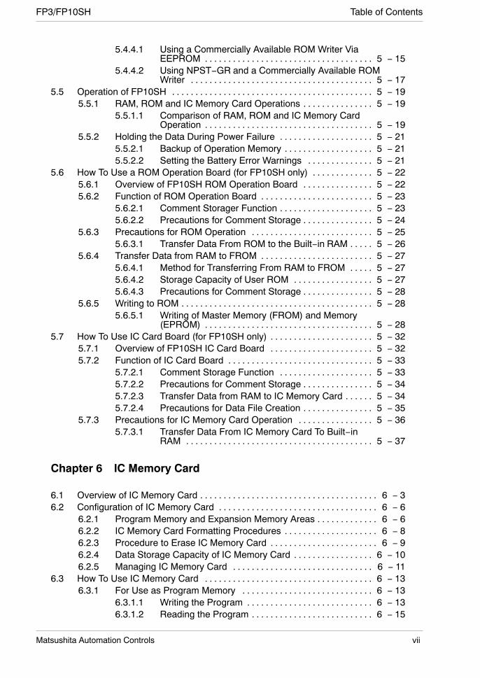
Table of ContentsFP3/FP10SH
viiMatsushita Automation Controls
5.4.4.1 Using a Commercially Available ROM Writer ViaEEPROM 5 − 15. . . . . . . . . . . . . . . . . . . . . . . . . . . . . . . . . . . .
5.4.4.2 Using NPST−GR and a Commercially Available ROMWriter 5 − 17. . . . . . . . . . . . . . . . . . . . . . . . . . . . . . . . . . . . . . .
5.5 Operation of FP10SH 5 − 19. . . . . . . . . . . . . . . . . . . . . . . . . . . . . . . . . . . . . . . . . . .5.5.1 RAM, ROM and IC Memory Card Operations 5 − 19. . . . . . . . . . . . . . .
5.5.1.1 Comparison of RAM, ROM and IC Memory CardOperation 5 − 19. . . . . . . . . . . . . . . . . . . . . . . . . . . . . . . . . . . .
5.5.2 Holding the Data During Power Failure 5 − 21. . . . . . . . . . . . . . . . . . . .5.5.2.1 Backup of Operation Memory 5 − 21. . . . . . . . . . . . . . . . . . .5.5.2.2 Setting the Battery Error Warnings 5 − 21. . . . . . . . . . . . . .
5.6 How To Use a ROM Operation Board (for FP10SH only) 5 − 22. . . . . . . . . . . . .5.6.1 Overview of FP10SH ROM Operation Board 5 − 22. . . . . . . . . . . . . . .5.6.2 Function of ROM Operation Board 5 − 23. . . . . . . . . . . . . . . . . . . . . . . .
5.6.2.1 Comment Storager Function 5 − 23. . . . . . . . . . . . . . . . . . . .5.6.2.2 Precautions for Comment Storage 5 − 24. . . . . . . . . . . . . . .
5.6.3 Precautions for ROM Operation 5 − 25. . . . . . . . . . . . . . . . . . . . . . . . . .5.6.3.1 Transfer Data From ROM to the Built−in RAM 5 − 26. . . . .
5.6.4 Transfer Data from RAM to FROM 5 − 27. . . . . . . . . . . . . . . . . . . . . . . .5.6.4.1 Method for Transferring From RAM to FROM 5 − 27. . . . .5.6.4.2 Storage Capacity of User ROM 5 − 27. . . . . . . . . . . . . . . . .5.6.4.3 Precautions for Comment Storage 5 − 28. . . . . . . . . . . . . . .
5.6.5 Writing to ROM 5 − 28. . . . . . . . . . . . . . . . . . . . . . . . . . . . . . . . . . . . . . . . .5.6.5.1 Writing of Master Memory (FROM) and Memory
(EPROM) 5 − 28. . . . . . . . . . . . . . . . . . . . . . . . . . . . . . . . . . . .5.7 How To Use IC Card Board (for FP10SH only) 5 − 32. . . . . . . . . . . . . . . . . . . . . .
5.7.1 Overview of FP10SH IC Card Board 5 − 32. . . . . . . . . . . . . . . . . . . . . .5.7.2 Function of IC Card Board 5 − 33. . . . . . . . . . . . . . . . . . . . . . . . . . . . . . .
5.7.2.1 Comment Storage Function 5 − 33. . . . . . . . . . . . . . . . . . . .5.7.2.2 Precautions for Comment Storage 5 − 34. . . . . . . . . . . . . . .5.7.2.3 Transfer Data from RAM to IC Memory Card 5 − 34. . . . . .5.7.2.4 Precautions for Data File Creation 5 − 35. . . . . . . . . . . . . . .
5.7.3 Precautions for IC Memory Card Operation 5 − 36. . . . . . . . . . . . . . . .5.7.3.1 Transfer Data From IC Memory Card To Built−in
RAM 5 − 37. . . . . . . . . . . . . . . . . . . . . . . . . . . . . . . . . . . . . . . .
Chapter 6 IC Memory Card
6.1 Overview of IC Memory Card 6 − 3. . . . . . . . . . . . . . . . . . . . . . . . . . . . . . . . . . . . . .6.2 Configuration of IC Memory Card 6 − 6. . . . . . . . . . . . . . . . . . . . . . . . . . . . . . . . . .
6.2.1 Program Memory and Expansion Memory Areas 6 − 6. . . . . . . . . . . . .6.2.2 IC Memory Card Formatting Procedures 6 − 8. . . . . . . . . . . . . . . . . . . .6.2.3 Procedure to Erase IC Memory Card 6 − 9. . . . . . . . . . . . . . . . . . . . . . .6.2.4 Data Storage Capacity of IC Memory Card 6 − 10. . . . . . . . . . . . . . . . .6.2.5 Managing IC Memory Card 6 − 11. . . . . . . . . . . . . . . . . . . . . . . . . . . . . .
6.3 How To Use IC Memory Card 6 − 13. . . . . . . . . . . . . . . . . . . . . . . . . . . . . . . . . . . .6.3.1 For Use as Program Memory 6 − 13. . . . . . . . . . . . . . . . . . . . . . . . . . . .
6.3.1.1 Writing the Program 6 − 13. . . . . . . . . . . . . . . . . . . . . . . . . . .6.3.1.2 Reading the Program 6 − 15. . . . . . . . . . . . . . . . . . . . . . . . . .
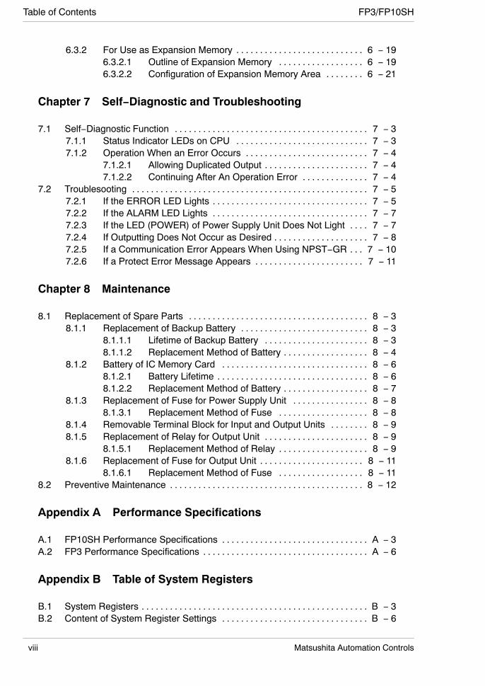
Table of Contents FP3/FP10SH
viii Matsushita Automation Controls
6.3.2 For Use as Expansion Memory 6 − 19. . . . . . . . . . . . . . . . . . . . . . . . . . .6.3.2.1 Outline of Expansion Memory 6 − 19. . . . . . . . . . . . . . . . . .6.3.2.2 Configuration of Expansion Memory Area 6 − 21. . . . . . . .
Chapter 7 Self−Diagnostic and Troubleshooting
7.1 Self−Diagnostic Function 7 − 3. . . . . . . . . . . . . . . . . . . . . . . . . . . . . . . . . . . . . . . . .7.1.1 Status Indicator LEDs on CPU 7 − 3. . . . . . . . . . . . . . . . . . . . . . . . . . . .7.1.2 Operation When an Error Occurs 7 − 4. . . . . . . . . . . . . . . . . . . . . . . . . .
7.1.2.1 Allowing Duplicated Output 7 − 4. . . . . . . . . . . . . . . . . . . . . .7.1.2.2 Continuing After An Operation Error 7 − 4. . . . . . . . . . . . . .
7.2 Troublesooting 7 − 5. . . . . . . . . . . . . . . . . . . . . . . . . . . . . . . . . . . . . . . . . . . . . . . . . .7.2.1 If the ERROR LED Lights 7 − 5. . . . . . . . . . . . . . . . . . . . . . . . . . . . . . . . .7.2.2 If the ALARM LED Lights 7 − 7. . . . . . . . . . . . . . . . . . . . . . . . . . . . . . . . .7.2.3 If the LED (POWER) of Power Supply Unit Does Not Light 7 − 7. . . .7.2.4 If Outputting Does Not Occur as Desired 7 − 8. . . . . . . . . . . . . . . . . . . .7.2.5 If a Communication Error Appears When Using NPST−GR 7 − 10. . .7.2.6 If a Protect Error Message Appears 7 − 11. . . . . . . . . . . . . . . . . . . . . . .
Chapter 8 Maintenance
8.1 Replacement of Spare Parts 8 − 3. . . . . . . . . . . . . . . . . . . . . . . . . . . . . . . . . . . . . .8.1.1 Replacement of Backup Battery 8 − 3. . . . . . . . . . . . . . . . . . . . . . . . . . .
8.1.1.1 Lifetime of Backup Battery 8 − 3. . . . . . . . . . . . . . . . . . . . . .8.1.1.2 Replacement Method of Battery 8 − 4. . . . . . . . . . . . . . . . . .
8.1.2 Battery of IC Memory Card 8 − 6. . . . . . . . . . . . . . . . . . . . . . . . . . . . . . .8.1.2.1 Battery Lifetime 8 − 6. . . . . . . . . . . . . . . . . . . . . . . . . . . . . . . .8.1.2.2 Replacement Method of Battery 8 − 7. . . . . . . . . . . . . . . . . .
8.1.3 Replacement of Fuse for Power Supply Unit 8 − 8. . . . . . . . . . . . . . . .8.1.3.1 Replacement Method of Fuse 8 − 8. . . . . . . . . . . . . . . . . . .
8.1.4 Removable Terminal Block for Input and Output Units 8 − 9. . . . . . . .8.1.5 Replacement of Relay for Output Unit 8 − 9. . . . . . . . . . . . . . . . . . . . . .
8.1.5.1 Replacement Method of Relay 8 − 9. . . . . . . . . . . . . . . . . . .8.1.6 Replacement of Fuse for Output Unit 8 − 11. . . . . . . . . . . . . . . . . . . . . .
8.1.6.1 Replacement Method of Fuse 8 − 11. . . . . . . . . . . . . . . . . .8.2 Preventive Maintenance 8 − 12. . . . . . . . . . . . . . . . . . . . . . . . . . . . . . . . . . . . . . . . .
Appendix A Performance Specifications
A.1 FP10SH Performance Specifications A − 3. . . . . . . . . . . . . . . . . . . . . . . . . . . . . . .A.2 FP3 Performance Specifications A − 6. . . . . . . . . . . . . . . . . . . . . . . . . . . . . . . . . . .
Appendix B Table of System Registers
B.1 System Registers B − 3. . . . . . . . . . . . . . . . . . . . . . . . . . . . . . . . . . . . . . . . . . . . . . . .B.2 Content of System Register Settings B − 6. . . . . . . . . . . . . . . . . . . . . . . . . . . . . . .
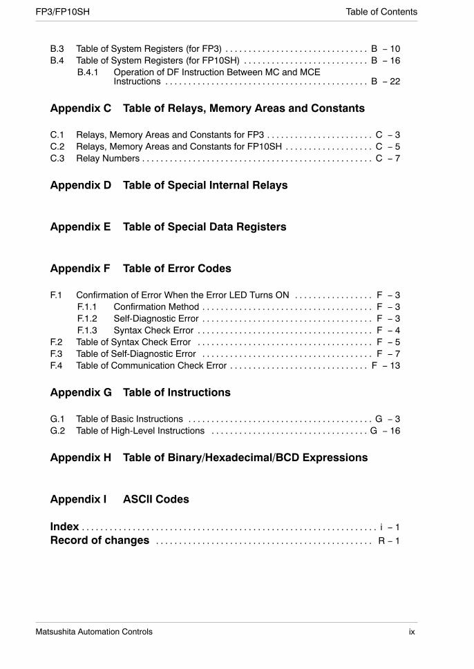
Table of ContentsFP3/FP10SH
ixMatsushita Automation Controls
B.3 Table of System Registers (for FP3) B − 10. . . . . . . . . . . . . . . . . . . . . . . . . . . . . . .B.4 Table of System Registers (for FP10SH) B − 16. . . . . . . . . . . . . . . . . . . . . . . . . . .
B.4.1 Operation of DF Instruction Between MC and MCEInstructions B − 22. . . . . . . . . . . . . . . . . . . . . . . . . . . . . . . . . . . . . . . . . . . .
Appendix C Table of Relays, Memory Areas and Constants
C.1 Relays, Memory Areas and Constants for FP3 C − 3. . . . . . . . . . . . . . . . . . . . . . .C.2 Relays, Memory Areas and Constants for FP10SH C − 5. . . . . . . . . . . . . . . . . . .C.3 Relay Numbers C − 7. . . . . . . . . . . . . . . . . . . . . . . . . . . . . . . . . . . . . . . . . . . . . . . . . .
Appendix D Table of Special Internal Relays
Appendix E Table of Special Data Registers
Appendix F Table of Error Codes
F.1 Confirmation of Error When the Error LED Turns ON F − 3. . . . . . . . . . . . . . . . .F.1.1 Confirmation Method F − 3. . . . . . . . . . . . . . . . . . . . . . . . . . . . . . . . . . . . .F.1.2 Self-Diagnostic Error F − 3. . . . . . . . . . . . . . . . . . . . . . . . . . . . . . . . . . . . .F.1.3 Syntax Check Error F − 4. . . . . . . . . . . . . . . . . . . . . . . . . . . . . . . . . . . . . .
F.2 Table of Syntax Check Error F − 5. . . . . . . . . . . . . . . . . . . . . . . . . . . . . . . . . . . . . .F.3 Table of Self-Diagnostic Error F − 7. . . . . . . . . . . . . . . . . . . . . . . . . . . . . . . . . . . . .F.4 Table of Communication Check Error F − 13. . . . . . . . . . . . . . . . . . . . . . . . . . . . . .
Appendix G Table of Instructions
G.1 Table of Basic Instructions G − 3. . . . . . . . . . . . . . . . . . . . . . . . . . . . . . . . . . . . . . . .G.2 Table of High-Level Instructions G − 16. . . . . . . . . . . . . . . . . . . . . . . . . . . . . . . . . .
Appendix H Table of Binary/Hexadecimal/BCD Expressions
Appendix I ASCII Codes
Index i − 1. . . . . . . . . . . . . . . . . . . . . . . . . . . . . . . . . . . . . . . . . . . . . . . . . . . . . . . . . . . . . . . .Record of changes R − 1. . . . . . . . . . . . . . . . . . . . . . . . . . . . . . . . . . . . . . . . . . . . . . .
Before You Start FP3/FP10SH
x Matsushita Automation Controls
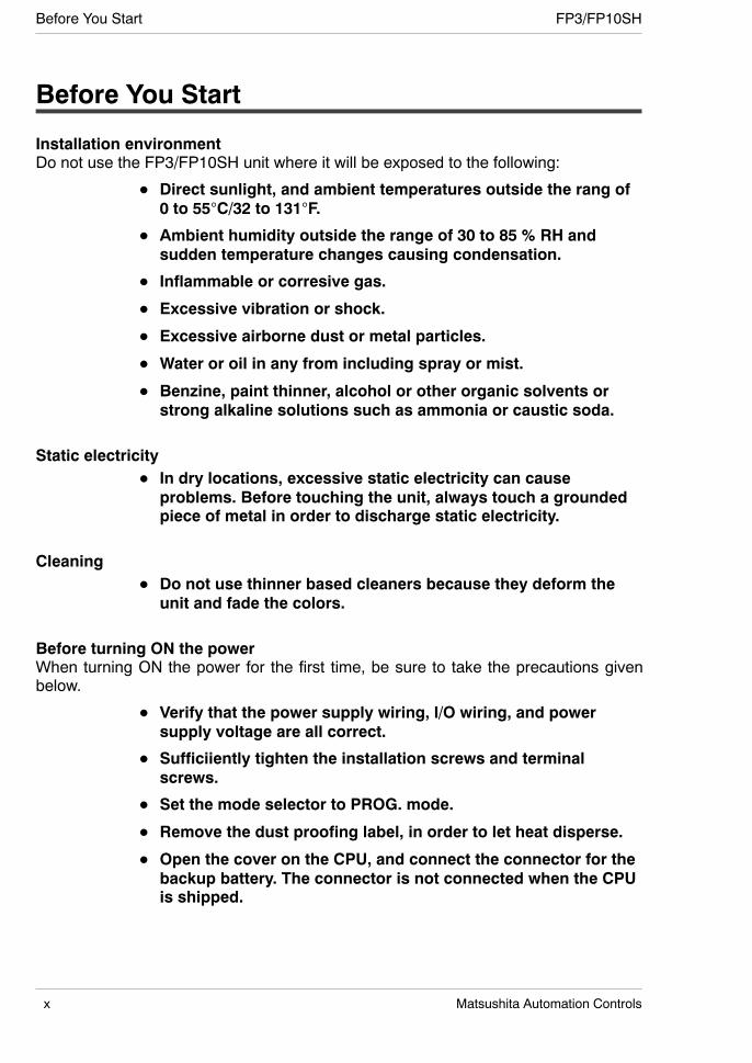
Before You Start
Installation environmentDo not use the FP3/FP10SH unit where it will be exposed to the following:
Direct sunlight, and ambient temperatures outside the rang of0 to 55°C/32 to 131°F.
Ambient humidity outside the range of 30 to 85 % RH andsudden temperature changes causing condensation.
Inflammable or corresive gas.
Excessive vibration or shock.
Excessive airborne dust or metal particles.
Water or oil in any from including spray or mist.
Benzine, paint thinner, alcohol or other organic solvents orstrong alkaline solutions such as ammonia or caustic soda.
Static electricityIn dry locations, excessive static electricity can causeproblems. Before touching the unit, always touch a groundedpiece of metal in order to discharge static electricity.
CleaningDo not use thinner based cleaners because they deform theunit and fade the colors.
Before turning ON the powerWhen turning ON the power for the first time, be sure to take the precautions givenbelow.
Verify that the power supply wiring, I/O wiring, and powersupply voltage are all correct.
Sufficiiently tighten the installation screws and terminalscrews.
Set the mode selector to PROG. mode.
Remove the dust proofing label, in order to let heat disperse.
Open the cover on the CPU, and connect the connector for thebackup battery. The connector is not connected when the CPUis shipped.

Before You StartFP3/FP10SH
xiMatsushita Automation Controls
Hardware compatibility between the two modelsThe FP3 and FP10SH share the same backplane and unit, but the following pointsshould be checked if the type of CPU is changed.
The internal current consumption varies depending on the CPU.See section 1.3.3, and check the total current consumption.
With the FP10SH, there are some expansion cables which cannot beused. See section 2.3 to check which cables can be used.
On the FP3, the programming tool port is an RS422 port (a 15−pinconnector), and on the FP10SH, the port is an RS232C port (a 9−pinconnector). The cables used for the two ports are different.
Programming toolsWhen using the NPST−GR software:
An adapter and cable are required to connect the FP3/FP10SH to acomputer (* section 1.5.2).
With the FP10SH, NPST−GR Ver.4 or a subsequent version is required.When using the handy−type FP programmer:
With the FP3, use “FP Programmer II Ver.2 (AFP1114V2).
The FP programmer cable (AFP5520: 50cm/19.69 in. or AFP5523:3 m/9.84 ft.) is required to connect the FP3 and the FP programmer IIVer.2.
. Note
The FP Programmer II Ver.2 cannot be used with the FP10SH.
Precautions when using the FP10SHWhen using the units listed below in combination with the FP10SH CPU, check theversion and lot number of the unit.
Type Ordernumber
Version/Lot number
A/D converter unitG type
AFP3402AFP3403AFP3405
The unit can be used if the lot number is97***** or a subsequent number.(Products manufactured in fiscal 1997 orlate )A/D converter unit
I typeAFP3406AFP3407AFP3408
later)
Positioning unitE type
AFP3431EAFP3432E
The unit can be used if the version is Ver.1.5 or a subsequent version.
Computer communicationunit (C.C.U.)
AFP3462 The unit can be used if the version is Ver.1.2 or a subsequent version.
Before You Start FP3/FP10SH
xii Matsushita Automation Controls
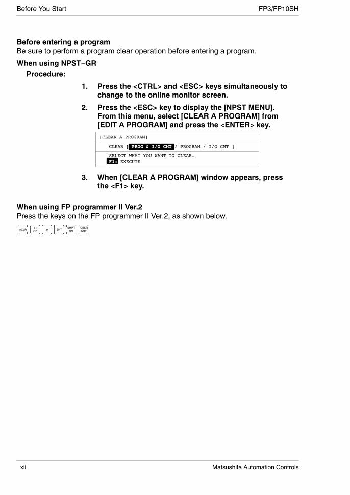
Before entering a programBe sure to perform a program clear operation before entering a program.
When using NPST−GRProcedure:
1. Press the <CTRL> and <ESC> keys simultaneously tochange to the online monitor screen.
2. Press the <ESC> key to display the [NPST MENU].From this menu, select [CLEAR A PROGRAM] from[EDIT A PROGRAM] and press the <ENTER> key.
[CLEAR A PROGRAM]
CLEAR [ PROG & I/O CMT / PROGRAM / I/O CMT ]
SELECT WHAT YOU WANT TO CLEAR.F1: EXECUTE
3. When [CLEAR A PROGRAM] window appears, pressthe <F1> key.
When using FP programmer II Ver.2Press the keys on the FP programmer II Ver.2, as shown below.
ENTACLR OP(−)
0 SCSHIFT
INST(DELT)
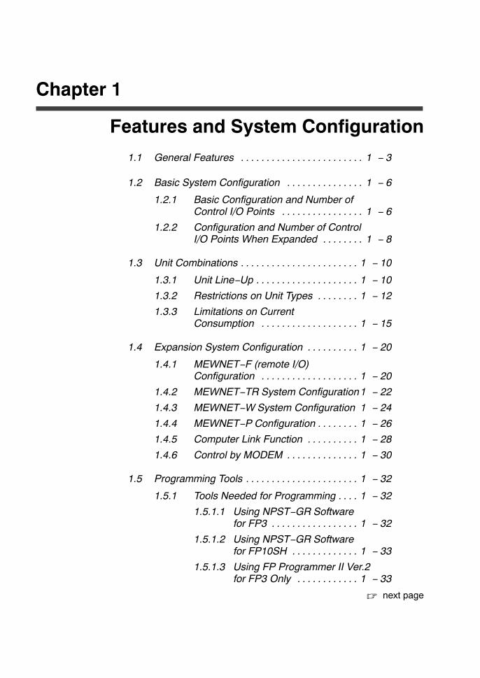
Chapter 1
Features and System Configuration
1.1 General Features 1 − 3. . . . . . . . . . . . . . . . . . . . . . . .
1.2 Basic System Configuration 1 − 6. . . . . . . . . . . . . . .
1.2.1 Basic Configuration and Number ofControl I/O Points 1 − 6. . . . . . . . . . . . . . . .
1.2.2 Configuration and Number of ControlI/O Points When Expanded 1 − 8. . . . . . . .
1.3 Unit Combinations 1 − 10. . . . . . . . . . . . . . . . . . . . . . .
1.3.1 Unit Line−Up 1 − 10. . . . . . . . . . . . . . . . . . . .
1.3.2 Restrictions on Unit Types 1 − 12. . . . . . . .
1.3.3 Limitations on CurrentConsumption 1 − 15. . . . . . . . . . . . . . . . . . .
1.4 Expansion System Configuration 1 − 20. . . . . . . . . .
1.4.1 MEWNET−F (remote I/O)Configuration 1 − 20. . . . . . . . . . . . . . . . . . .
1.4.2 MEWNET−TR System Configuration1 − 22
1.4.3 MEWNET−W System Configuration 1 − 24
1.4.4 MEWNET−P Configuration 1 − 26. . . . . . . .
1.4.5 Computer Link Function 1 − 28. . . . . . . . . .
1.4.6 Control by MODEM 1 − 30. . . . . . . . . . . . . .
1.5 Programming Tools 1 − 32. . . . . . . . . . . . . . . . . . . . . .
1.5.1 Tools Needed for Programming 1 − 32. . . .
1.5.1.1 Using NPST−GR Softwarefor FP3 1 − 32. . . . . . . . . . . . . . . . .
1.5.1.2 Using NPST−GR Softwarefor FP10SH 1 − 33. . . . . . . . . . . . .
1.5.1.3 Using FP Programmer II Ver.2for FP3 Only 1 − 33. . . . . . . . . . . .
next page
I/O Allocation FP3/FP10SH
1 − 2 Matsushita Automation Controls
1.5.2 Table of Programming Tools 1 − 34. . . . . .
1.5.3 Tools Needed for ROM Writingof FP3 1 − 35. . . . . . . . . . . . . . . . . . . . . . . . .
1.5.3.1 When Creating a ROM With aCommercially Available ROMWriter, Through a MasterMemory (EEPROM) 1 − 35. . . . . .
1.5.3.2 When Creating a ROM WithNPST−GR Software and aCommercially Available ROMWriter 1 − 36. . . . . . . . . . . . . . . . . .
1.5.4 Tools Needed for ROM Writingof FP10SH 1 − 37. . . . . . . . . . . . . . . . . . . . .
1.5.4.1 When Creating a ROM With aCommercially Available ROMWriter, Through a MasterMemory (FROM) 1 − 37. . . . . . . . .
1.5.4.2 When Creating a ROM WithNPST−GR Software and aCommercially Available ROMWriter 1 − 38. . . . . . . . . . . . . . . . . .

I/O AllocationFP3/FP10SH
1 − 3Matsushita Automation Controls
1.1 General Features
1.1 General FeaturesExclusive RISC (Reduced instruction set computer) processor for high speedprocessing.
Basic sequence instructions: 40 ns
Timer, counter instructions: 280 ns
Data transfer instructions: 80 ns
Addition/subtraction instructions: 240 ns
Scan time of 1 ms (for 10 k steps)The time required for one scan is greatly reduced by paralleling the calculation andtransmission processes.
Large program memory with a maximum of 120 k stepsCPU with an internal RAM capacity of 30 k steps. With the addition of the FP10SHoptional expansion memory unit of 30 k (or 90 k) steps, a programming capacity of upto 60 k (or 120 k) steps can be obtained.
Expansion memory unit
Transmission port with 115 kbps capabilityGreatly increased transmission speed means the program upload and downloadprocessing speeds are also greatly increased.
Functions demanded from larger modules are added1 ms unit timer added.
Real number calculations (trigonometric functions, exponents,logarithms, square roots, etc.)
Index modifier functions (224 words with bit modifier is also possible)
I/O Allocation FP3/FP10SH
1 − 4 Matsushita Automation Controls
1.1 General Features
ROM and IC memory card available for optional memoryProgram memory can be converted to ROM (with use of optional ROMoperation board).
Supports the use of IC memory cards for use as program memory orexpansion data memory (with use of optional IC memory card board).
ROM operation board IC memory card board
CPU comes standard with RS232C port
Hardware and software designed with considerations for expansionWith few restrictions when using units in combinations, up to 512 points are possiblewith an 8−slot master backplane and 64−point units, and this is expandable to up to1,536 points with additional backplanes (up to 2,048 with the FP10SH). Remodelingand expansion of the equipment is also supported for greater flexibility.
3 4 5 6 7 8
1 2 3 4 5 6 7 8
1 2 3 4 5 6 7 8
Masterbackplane
1stexpansionbackplane
1 2
(*) The FP10SH CPU supports expansion of up to 3 expansion backplanes.
1 2 3 4 5 6 7 8
Max.512 points
Max.2048 points (*)
Max.1024 points
Max.1536 points
2ndexpansionbackplane
3rdexpansionbackplane
Common programming software (NPST−GR software)Our FP series also supports the same programming software to allow you to make useof the same programs used with the smaller programmable controllers.
I/O AllocationFP3/FP10SH
1 − 5Matsushita Automation Controls
1.1 General Features
Copious selection of unitsInput units (16 points, 32 points, 64 points)
Output units (16 points, 32 points, 64 points)
I/O units (3 types)
Remote I/O-related units (2 types)
Analog I/O units (7 types)
Serial data controller units (2 types)
Positioning control units (4 types)
Interrupt control unit (1 type)
Link system-related units (5 types)
Standard modem initialization functionAmodem can be connected to the CPU for use with programmaintenance systems andremote monitoring and observation systems over normal phone lines.
Expandable over existing networksBesides MEWNET−F (remote I/O) systems, the units can be networked betweenprogrammable controllers and computers. Units with Ethernet capabilities (ET−LANunits) are also available.
Comparison of processing speed and memory capacity
Item FP10SH FP3
AFP6221V3 AFP6211V3 AFP3220C−F AFP3210C−FAFP3211C−F
Processingspeed (per an
Sequenceinstruction
0.04 µs 0.1 µs 0.5 µsspeed (pe ainstruction) Timer
instruction0.28 µs 0.7 µs 2.0 µs
High−levelinstruction
from 0.08 µs from 0.2 µs from dozens of speed µs
Program capacity 30 k steps(expanded up to 120 k steps)
16 k steps 10 k steps
External input relays (X) 8,192 points 2,048 pointsExternal output relays (Y) 8,192 points 2,048 pointsInternal relays (R) 14,192 points 1,568 pointsData registers (DT) 10,240 words 2,048 wordsFile registers (FL) 32,765 words 22,525 words to 0 wordLink relays (L) 10,240 points 1,024 points× 2Link data registers (LD) 8,448 words 128 words× 2
I/O Allocation FP3/FP10SH
1 − 6 Matsushita Automation Controls
1.2 Basic System Configuration
1.2 Basic System Configuration
1.2.1 Basic Configuration and Number of Control I/O Points
Item Master backplane
3-slottype
48 I/O points: using three 16-point I/O units96 I/O points: using three 32-point I/O units192 I/O points: using three 64-point I/O units
Power supplyunit
CPU
5-slottype
80 I/O points: using 16-point five I/O units160 I/O points: using 32-point five I/O units320 I/O points: using 64-point five I/O units
Power supply unit CPU
8-slottype
128 I/O points: using eight 16-point I/O units256 I/O points: using eight 32-point I/O units512 I/O points: using eight 64-point I/O units
Power supply unit CPU
Item Expansion backplane
3-slottype
48 I/O points: using three 16-point I/O units96 I/O points: using three 32-point I/O units192 I/O points: using three 64-point I/O units
Power supply unit
5-slottype
80 I/O points: using five 16-point I/O units160 I/O points: using five 32-point I/O units320 I/O points: using five 64-point I/O units
Power supply unit
8-slottype
128 I/O points: using eight 16-point I/O units256 I/O points: using eight 32-point I/O units512 I/O points: using eight 64-point I/O units
Power supply unit
next page

I/O AllocationFP3/FP10SH
1 − 7Matsushita Automation Controls
1.2 Basic System Configuration
The I/O units, intelligent units, power supply unit and backplane can be commonly usedfor the FP3 and the FP10SH.Although most of the I/O units and intelligent units can be combined freely in the layout,you should check the following points when selecting your units:
− the restrictions on unit types (* section 1.3.2).
− the limitations on current consumption (* section 1.3.3).The mounting position for the I/O units on each backplane are free and the I/O can beassigned using NPST-GR, so system design and specifications changes are easilysupported.The master and expansion backplanes are available in three types: 3-slot, 5-slot and8-slot.The number of I/O points controllable for one backplane for 16−point, 32−point, and64−point I/O units as shown below.
Backplane type Using 16−pointI/O units
Using 32−pointI/O units
Using 64−pointI/O units
3−slot 48 points 96 points 192 points
5−slot 80 points 160 points 320 points
8−slot 128 points 256 points 512 points

I/O Allocation FP3/FP10SH
1 − 8 Matsushita Automation Controls
1.2 Basic System Configuration
1.2.2 Configuration and Number of Control I/O Points When Expanded
Expansion cable
FP3 FP10SH
Masterbackplane
Expansionbackplane(No.1)
Expansionbackplane(No.2)
Masterbackplane
Expansionbackplane(No.1)
Expansionbackplane(No.2)
Expansionbackplane(No.3)
Expansion cable
Expansion cable
Expansion cable
Expansion cable
Both master and expansion backplanes can be connected in any combination between3−, 5− and 8−slot types.
Up to two (for the FP3) or three (for the FP10SH) expansion backplanes can beconnected to a master backplane.When using 64−point units attached to 8−slot backplanes, up to the following numberof points become controllable.
FP3Masterbackplane
Expansionbackplane
Expansionbackplane
512 points + 512 points + 512 points = total 1,536 points
FP10SHMasterbackplane
Expansionbackplane
Expansionbackplane
512 points + 512 points + 512 points
Expansionbackplane
+ 512 points = total 2,048 points
For limitation on expansion of the expansion cable, refer to section 2.3.
I/O AllocationFP3/FP10SH
1 − 9Matsushita Automation Controls
1.2 Basic System Configuration
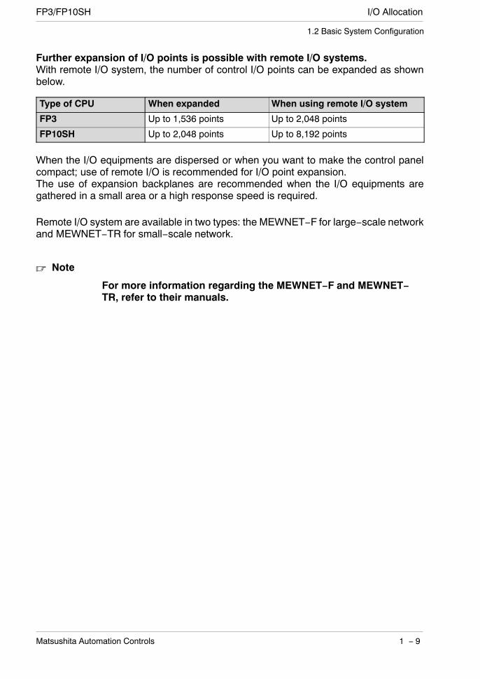
Further expansion of I/O points is possible with remote I/O systems.With remote I/O system, the number of control I/O points can be expanded as shownbelow.
Type of CPU When expanded When using remote I/O system
FP3 Up to 1,536 points Up to 2,048 points
FP10SH Up to 2,048 points Up to 8,192 points
When the I/O equipments are dispersed or when you want to make the control panelcompact; use of remote I/O is recommended for I/O point expansion.The use of expansion backplanes are recommended when the I/O equipments aregathered in a small area or a high response speed is required.
Remote I/O system are available in two types: the MEWNET−F for large−scale networkand MEWNET−TR for small−scale network.
Note
For more information regarding the MEWNET−F and MEWNET−TR, refer to their manuals.

I/O Allocation FP3/FP10SH
1 − 10 Matsushita Automation Controls
1.3 Unit Combinations
1.3 Unit Combinations
1.3.1 Unit Line−Up
Power supplydummy unit
3-slot type
CPU(with built−inRAM)
Optional memory
An expansionmemory unit(RAM) isavailable forthe FP10SH.
FP3CPU
FP10SHCPU
For FP3
EPROM orEEPROM
IC memorycard(SRAM/FROM)
This unit need to beinstalled when beingused as a slave stationof the MEWNET−F(remote I/O) system.
100/200 V AC type(selectable)
24 V DC type
For FP10SH
EPROM orFROM
A ROM operation board or IC memorycard board is required when optionalmemory is used for FP10SH.
5-slot type
8-slot type
3-slot type
5-slot type
8-slot type
Power supply unit
MEWNET-F (remote I/O) slave unit

I/O AllocationFP3/FP10SH
1 − 11Matsushita Automation Controls
1.3 Unit Combinations
32 pointsDC type
64 pointsDC type
8 pointsAC type
16 pointsAC type
16 pointsRelay type
16 pointsTransistortype
32 pointsTransistortype
64 pointsTransistortype
16 pointTriac type
16 pointsDC type
I:8/O:8,DC input/Relay type
I:32/O:32,DC input/Transistor type
Input units Output units
I/O mixed units Remote I/O-related units
MEWNET-F(remote I/O)master unit
MEWNET-TRmaster unit
Analog I/O units Operation display paneland computer interface unit Serial data controller units
Position control and motor control units Interrupt unit
Link system-related units Expansion data memory unit
A/Dconverterunit
RTD inputunit
Thermocoupleinput unit
D/Aconverterunit
Computer communicationunit (C.C.U.)
Serialdata unit
Data processunit
High-speedcounter unit
Positioningunit F-type(transistor type)
Pulseoutput unit
Positioningunit E-type
Positioningunit F-type(Line−driver type)
Interrupt unit
ET-LAN linkunit
MEWNET-P(optical) link unit
MEWNET-W(wire) link unit
C-NET linkunit
Expansion data memory unit

I/O Allocation FP3/FP10SH
1 − 12 Matsushita Automation Controls
1.3 Unit Combinations
1.3.2 Restrictions on Unit Types
Combination of FP3/FP10SH units (A: Available, N/A: Not available)Basic Units
Backplanes and units
Set configurations
MasterBackplane
ExpansionBackplane
Power
SupplyUnit
CPU
MEWNET−F
(rem
oteI/O
)Slave
Unit
Basicset
Powersupplyunit
CPU I/O mountingarea
The most basic configurationfor CPU installation.Power supply unit and CPUare installed to a masterbackplane.
A N/A A A N/A
Expan-sion set
Powersupplyunit
I/O mountingarea
This configuration is tobe used for expansion.A power supply unit isinstalled to an expansionbackplane.
N/A A A(*)
N/A N/A
RemoteI/O slavestationset
Powersupplyunit
Slave I/O mountingarea
This configuration isused when the serves asslave station of MEWNET−F(remote I/O system).A power supply unit andremote I/O slave units areinstalled to a masterbackplane.
A N/A A N/A A
Note(*): A power supply dummy unit may be used to omit the power
supply unit (* section 2.7).
I/O AllocationFP3/FP10SH
1 − 13Matsushita Automation Controls
1.3 Unit Combinations
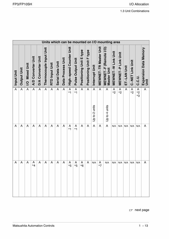
Units which can be mounted on I/O mounting area
InputUnit
OutputUnit
I/OMixed
Unit
A/D
Converter
Unit
D/A
Converter
Unit
ThermocoupleInputUnit
RTDInputUnit
SerialD
ataUnit
DataProcess
Unit
High−speedCounter
Unit
PulseOutputUnit
PositioningUnitEtype
PositioningUnitFtype
InterruptUnit
MEWNET−TR
MasterUnit
MEWNET−F
(Rem
oteI/O
)MasterUnit
MEWNET−W
LinkUnit
MEWNET−P
LinkUnit
ET−LANUnit
C−N
ETLinkUnit
C.C.U.
ExpansionDataMem
ory
Unit
A A A A A A A A A A*1
A*1
A A A
Upto2units
A A
Upto4units
A*2
A*2
A A*2
A*2*3
A
A A A A A A A A A A*1
A*1
A A A A A N/A N/A N/A N/A N/A A
A A A A*4
A A A A A A*5
A*5
A*6
A N/A A*7
N/A N/A N/A N/A N/A N/A A
next page

I/O Allocation FP3/FP10SH
1 − 14 Matsushita Automation Controls
1.3 Unit Combinations
Notes
(*1): Interrupt function is available on high−speed counter andpulse output units when the total number of units is 8 orless.
(*2): Up to 3 units in all −MEWNET−W link unit, MEWNET−Plink unit, C−NET link unit and computer communicationunit (Up to 5 units in all if the CPU is the FP10SH).Up to 2 units in all −MEWNET−W and MEWNET−P− for PClink function.
(*3): When using the FP10SH, the computer communicationunit Ver. 1.2 or later is required.
(*4): When using the FP10SH, units producted in 1997 or laterare required for I and G types (lot No. of 97**** or later).
(*5): The interrupt function is not available when a remote I/Oslave unit is connected.
(*6): When using the FP10SH, the positioning unit E−type Ver.1.5 or later is required.
(*7): When using the FP10SH, the MEWNET−TR transmittermaster unit Ver.1.1 or later is required.
I/O AllocationFP3/FP10SH
1 − 15Matsushita Automation Controls
1.3 Unit Combinations
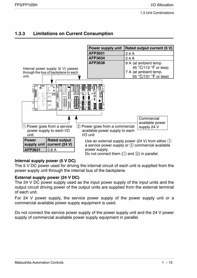
1.3.3 Limitations on Current Consumption
Internal power supply (5 V) passesthrough the bus of backplane to eachunit.
Powersupply unit
Rated outputcurrent (24 V)
AFP3631 0.8 A
Commercialavailable powersupply 24 V1 Power goes from a service
power supply to each I/Ounit
2 Power goes from a commercialavailable power supply to eachI/O unit
Use an external supply power (24 V) from either 1a service power supply or 2 commercial availablepower supply.Do not connect them ( 1 and 2 ) in parallel.
Power supply unit Rated output current (5 V)AFP3631AFP3634AFP3638
2.4 A2.4 A9 A (at ambient temp.
45 °C/113 °F or less)7 A (at ambient temp.
55 °C/131 °F or less)
Internal supply power (5 V DC)The 5 V DC power used for driving the internal circuit of each unit is supplied from thepower supply unit through the internal bus of the backplane.
External supply power (24 V DC)The 24 V DC power supply used as the input power supply of the input units and theoutput circuit driving power of the output units are supplied from the external terminalof each unit.For 24 V power supply, the service power supply of the power supply unit or acommercial available power supply equipment is used.
Do not connect the service power supply of the power supply unit and the 24 V powersupply of commercial available power supply equipment in parallel.
I/O Allocation FP3/FP10SH
1 − 16 Matsushita Automation Controls
1.3 Unit Combinations
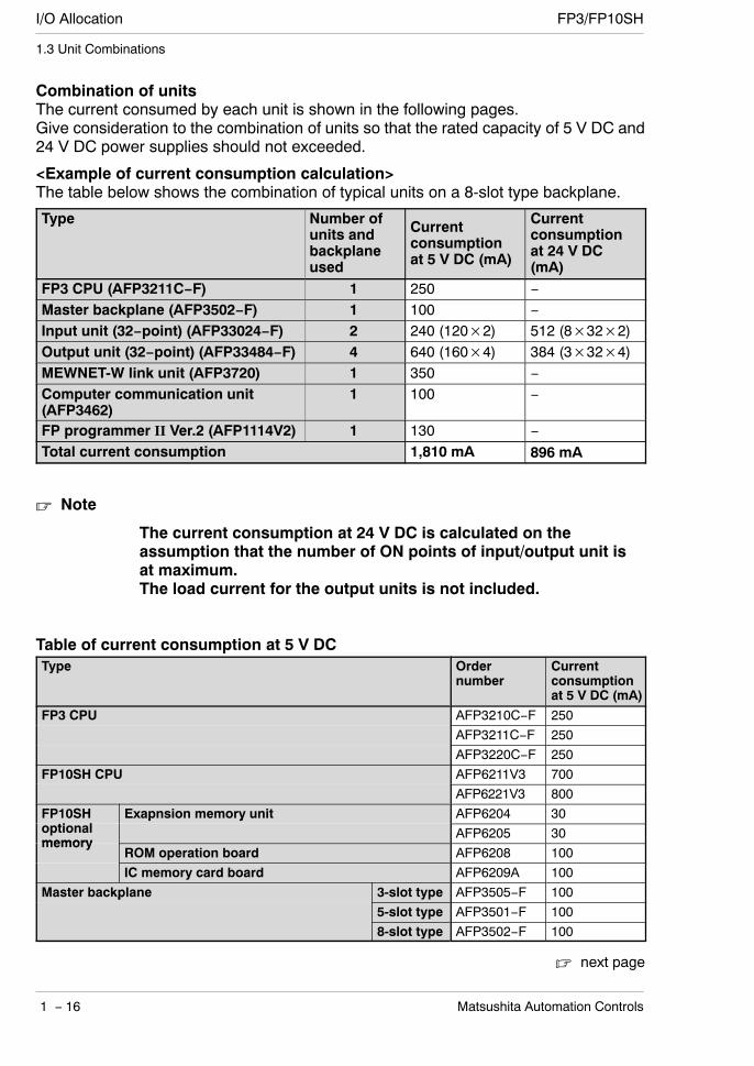
Combination of unitsThe current consumed by each unit is shown in the following pages.Give consideration to the combination of units so that the rated capacity of 5 V DC and24 V DC power supplies should not exceeded.
<Example of current consumption calculation>The table below shows the combination of typical units on a 8-slot type backplane.
Type Number ofunits andbackplaneused
Currentconsumptionat 5 V DC (mA)
Currentconsumptionat 24 V DC(mA)
FP3 CPU (AFP3211C−F) 1 250 −Master backplane (AFP3502−F) 1 100 −Input unit (32−point) (AFP33024−F) 2 240 (120×2) 512 (8×32×2)Output unit (32−point) (AFP33484−F) 4 640 (160×4) 384 (3×32×4)MEWNET-W link unit (AFP3720) 1 350 −Computer communication unit(AFP3462)
1 100 −
FP programmer II Ver.2 (AFP1114V2) 1 130 −Total current consumption 1,810 mA 896 mA
Note
The current consumption at 24 V DC is calculated on theassumption that the number of ON points of input/output unit isat maximum.The load current for the output units is not included.
Table of current consumption at 5 V DCType Order
numberCurrentconsumptionat 5 V DC (mA)
FP3 CPU AFP3210C−F 250AFP3211C−F 250AFP3220C−F 250
FP10SH CPU AFP6211V3 700AFP6221V3 800
FP10SHi l
Exapnsion memory unit AFP6204 30optionalmemory
p yAFP6205 30
memoryROM operation board AFP6208 100IC memory card board AFP6209A 100
Master backplane 3-slot type AFP3505−F 100p5-slot type AFP3501−F 1008-slot type AFP3502−F 100
next page
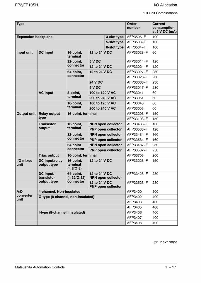
I/O AllocationFP3/FP10SH
1 − 17Matsushita Automation Controls
1.3 Unit Combinations
Type Ordernumber
Currentconsumptionat 5 V DC (mA)
Expansion backplane 3-slot type AFP3506−F 100p p5-slot type AFP3503−F 1008-slot type AFP3504−F 100
Input unit DC input 16-point,terminal
12 to 24 V DC AFP33023−F 60
32-point, 5 V DC AFP33014−F 120p ,connector 12 to 24 V DC AFP33024−F 12064-point, 12 to 24 V DC AFP33027−F 230p ,connector AFP33028−F 230
24 V DC AFP33068−F 2305 V DC AFP33017−F 230
AC input 8-point,i l
100 to 120 V AC AFP33041 60p p ,terminal 200 to 240 V AC AFP33051 6016-point,
i l100 to 120 V AC AFP33043 60p ,
terminal 200 to 240 V AC AFP33053 60Output unit Relay output 16-point, terminal AFP33203−F 150p y p
typep ,
AFP33103−F 150Transistor 16-point,
i lNPN open collector AFP33483−F 100
outputp ,
terminal PNP open collector AFP33583−F 12032-point, NPN open collector AFP33484−F 160p ,connector PNP open collector AFP33584−F 16064-point NPN open collector AFP33487−F 250pconnector PNP open collector AFP33587−F 250
Triac output 16-point, terminal AFP33703 200I/O mixedunit
DC input/relayoutput type
16-point,terminal(I: 8/O:8)
12 to 24 V DC AFP33223−F 150
DC input/transistor
64-point,(I: 32/O:32)
12 to 24 V DCNPN open collector
AFP33428−F 230transistoroutput type
(I: 32/O:32)connector 12 to 24 V DC
PNP open collectorAFP33528−F 230
A/D 4-channel, Non-insulated AFP3400 500/converterunit
G-type (8-channel, non-insulated) AFP3402 400unit
yp ( , )AFP3403 400AFP3405 400
I-type (8-channel, insulated) AFP3406 400yp ( , )AFP3407 400AFP3408 400
next page

I/O Allocation FP3/FP10SH
1 − 18 Matsushita Automation Controls
1.3 Unit Combinations
Type Ordernumber
Currentconsumptionat 5 V DC (mA)
D/A 2-channel (non-insulated) AFP3410 700/converterunit
( )AFP3411 700
unitI-type(i l d)
2-channel AFP3412 600yp(insulated) AFP3413 600
AFP3416 600AFP3417 600
4-channel AFP3414 1,000AFP3415 1,000AFP3418 1,000AFP3419 1,000
Thermocouple input unit AFP3420 500R.T.D. input unit AFP3421 500Serial data unit AFP3460 100Data process unit AFP3461 300High-speed counter unit 1-channel type AFP3621 150g p
2-channel type AFP3622 220Pulse output unit AFP3480 150Positioning unit E-type Transistor 1-axis type AFP3431E 250g yp
output type 2-axis type AFP3432E 250Positioning unit F-type Transistor 1-axis type AFP3431 350g yp
output type 2-axis type AFP3432 400Line-driver 1-axis type AFP3434 350output type 2-axis type AFP3435 350
3-axis type AFP3436 400Interrupt unit AFP3452 100MEWNET-TR master unit AFP3750 150MEWNET-F master unit AFP3742 450
slave unit AFP3743 400MEWNET-W link unit AFP3720 350MEWNET-P link unit AFP3710 320ET-LAN link unit AFP3790 470C-NET link unit AFP3463 350Computer communication unit (C.C.U.) AFP3462 100Expansion data memory unit AFP32091 50p y
AFP32092 50FP programmer II Ver.2 AFP1114V2 130Teaching unit II AFP5134 350

I/O AllocationFP3/FP10SH
1 − 19Matsushita Automation Controls
1.3 Unit Combinations
Table of current consumption at 24 V DCType Order
numberCurrentconsumptionat 24 V DC(mA)
Input unit DC input(12 2 V DC)
16-point, terminal AFP33023−F 8× np p(12 to 24 V DC) 32-point, connector AFP33024−F 8× n
64-point, connector AFP33027−F 6× np ,AFP33028−F 6× n
DC input(24 V DC)
64-point, connector AFP33068−F 3.5× n
Output unit Relay output 16-point, terminal AFP33203−F 10× np y ptype
p ,AFP33103−F 10× n
Transistor 16-point,i l
NPN open collector AFP33483−F 6× noutput
p ,terminal PNP open collector AFP33583−F 6× n32-point, NPN open collector AFP33484−F 3× np ,connector PNP open collector AFP33584−F 3× n64-point NPN open collector AFP33487−F 3× npconnector PNP open collector AFP33587−F 3× n
Notes
“n” expresses the number of inputs or outputs that are ON.
The input unit displays the current flowing to the internalcircuit. The other units display the current value required todrive the internal circuit. This value does not include the loadcurrent of the output unit.
Table of output current value of power supply unitPower supply unit Order number Rated output current (mA)pp y
at 5 V DC at 24 V DC100 V/200 V AC type AFP3631 2,400 800/ yp
AFP3638 7,000 (* Note 1)9,000 (* Note 2)
−−
24 V DC type AFP3634 2,400 −
Notes
(*1): At ambient temperature 55 °C/131.0 °F or less
(*2): At ambient temperature 45 °C/113.0 °F or less
I/O Allocation FP3/FP10SH
1 − 20 Matsushita Automation Controls
1.4 Expansion System Configuration
1.4 Expansion System Configuration
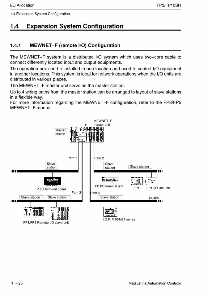
1.4.1 MEWNET−F (remote I/O) Configuration
The MEWNET−F system is a distributed I/O system which uses two−core cable toconnect differently located input and output equipments.The operation box can be installed in one location and used to control I/O equipmentin another locations. This system is ideal for network operations when the I/O units aredistributed in various places.The MEWNET−F master unit serve as the master station.Up to 4 wiring paths from the master station can be arranged to layout of slave stationsin a flexible way.For more information regarding the MEWNET−F configuration, refer to the FP3/FP5MEWNET−F manual.
Masterstation
Slavestation
Slavestation Slave station
Slave station Slave station Slave station
Path 1 Path 2
Path 3 Path 4
MEWNET−Fmaster unit
FP I/O terminal boardFP I/O terminal unit FP1
FP3/FP5 Remote I/O slave unitI.O.P. M30/M21 series
RS485
FP1 I/O link unit

I/O AllocationFP3/FP10SH
1 − 21Matsushita Automation Controls
1.4 Expansion System Configuration
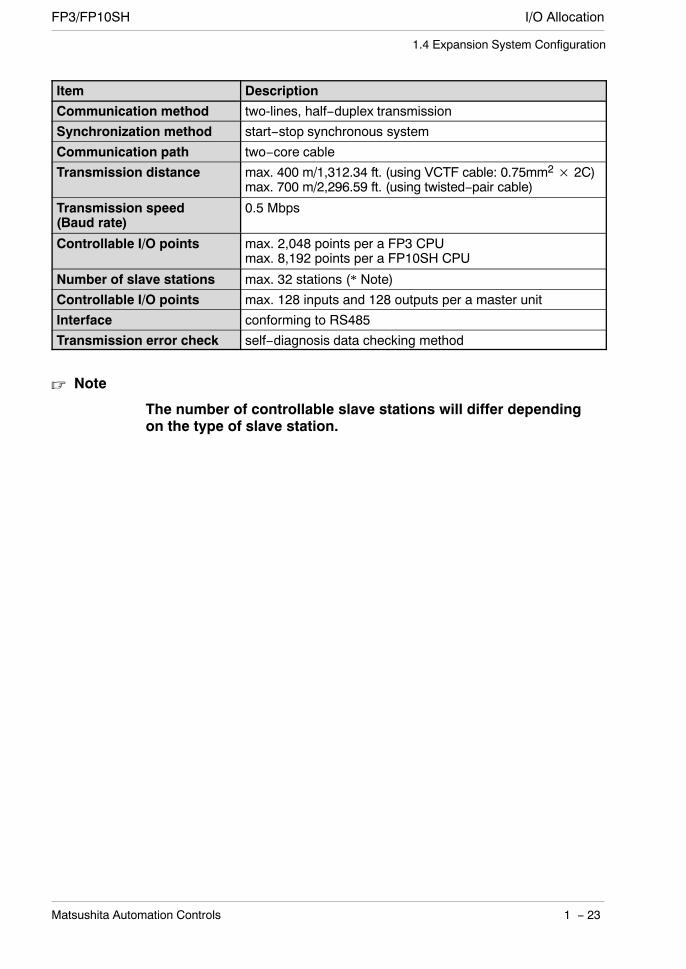
Item Description
Communication method two-line, half−duplex transmission
Synchronization method start−stop synchronous system
Communication path two−core cable(VCTF: 0.75 mm2× 2C or twisted−pair cable)
Transmission distance(* Note 1)
total distance:max. 400 m/1,312.34 ft. per port (using VCTF cable)max. 700 m/2,296.59 ft. per port (using twisted−paircable)
Transmission speed(Baud rate)
0.5 Mbps
Number of slave stations(* Note 2)
max. 32 stations per one master unit
Controllable I/O points max. 2,048 points per a FP3 CPUmax. 8,192 points per a FP10SH CPU
Interface conforming to RS485
Transmission error check CRC (Cyclic Redundancy Check) method
Notes
(*1): When using slave stations with conventional products(AFP87442, AFP3741, and AFP5741) on the same network,the maximum distance for transmissions is 200 m/656.168 ft. with VCTF cable and 300 m/984.252 ft. withtwisted−pair cable.
(*2): The number of controllable slave stations will differdepending on the type of slave station.

I/O Allocation FP3/FP10SH
1 − 22 Matsushita Automation Controls
1.4 Expansion System Configuration
1.4.2 MEWNET−TR System Configuration
This network system allows control with reduced cabling between the FP3 or FP10SHCPU and input/output units.By connecting the exclusive I/O terminal block, you can control the input and outputfrom the I/O terminal block (remote I/O control function).Allows the connection of two CPUs for the exchange of input/output information (I/O linkfunction).Equipped with a sefety function for selecting the operation status (operation stop modeor operation continue mode) when a communication error occurs.For more information regarding the MEWNET−TR configuration, refer to theMEWNET−TR manual.
FP I/O transmitter unit(4−input type, 4−output type)
Two−core cable(multi−drop wiring)
I/O link function
FP1 Control unit FP1 transmitter master unit
FP3 transmitter master unit
FP3 CPU or FP10SH CPU
Masterstation
Slavestation
FP I/O transmitter unit(8−input type, 8−output)
FP I/O transmitter unit(16−input type, 16−output type)
FP3 transmitter master unitFP3 transmitter master unit
Masterstation A
Masterstation A
Masterstation B
Masterstation B
FP3 transmitter master unitFP3 CPU or FP10SH CPU
Two−core cable
Remote I/O control function
I/O AllocationFP3/FP10SH
1 − 23Matsushita Automation Controls
1.4 Expansion System Configuration
Item Description
Communication method two-lines, half−duplex transmission
Synchronization method start−stop synchronous system
Communication path two−core cable
Transmission distance max. 400 m/1,312.34 ft. (using VCTF cable: 0.75mm2× 2C)max. 700 m/2,296.59 ft. (using twisted−pair cable)
Transmission speed(Baud rate)
0.5 Mbps
Controllable I/O points max. 2,048 points per a FP3 CPUmax. 8,192 points per a FP10SH CPU
Number of slave stations max. 32 stations (* Note)
Controllable I/O points max. 128 inputs and 128 outputs per a master unit
Interface conforming to RS485
Transmission error check self−diagnosis data checking method
Note
The number of controllable slave stations will differ dependingon the type of slave station.
I/O Allocation FP3/FP10SH
1 − 24 Matsushita Automation Controls
1.4 Expansion System Configuration
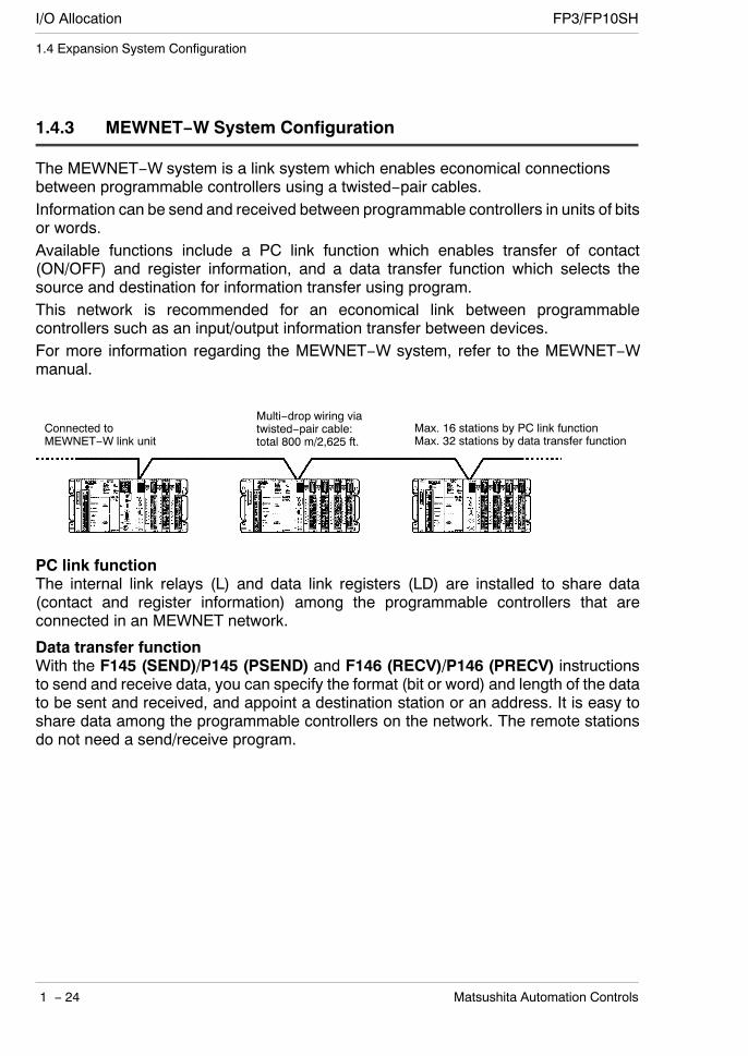
1.4.3 MEWNET−W System Configuration
The MEWNET−W system is a link system which enables economical connectionsbetween programmable controllers using a twisted−pair cables.Information can be send and received between programmable controllers in units of bitsor words.Available functions include a PC link function which enables transfer of contact(ON/OFF) and register information, and a data transfer function which selects thesource and destination for information transfer using program.This network is recommended for an economical link between programmablecontrollers such as an input/output information transfer between devices.For more information regarding the MEWNET−W system, refer to the MEWNET−Wmanual.
Connected toMEWNET−W link unit
Multi−drop wiring viatwisted−pair cable:total 800 m/2,625 ft.
Max. 16 stations by PC link functionMax. 32 stations by data transfer function
PC link functionThe internal link relays (L) and data link registers (LD) are installed to share data(contact and register information) among the programmable controllers that areconnected in an MEWNET network.
Data transfer functionWith the F145 (SEND)/P145 (PSEND) and F146 (RECV)/P146 (PRECV) instructionsto send and receive data, you can specify the format (bit or word) and length of the datato be sent and received, and appoint a destination station or an address. It is easy toshare data among the programmable controllers on the network. The remote stationsdo not need a send/receive program.
I/O AllocationFP3/FP10SH
1 − 25Matsushita Automation Controls
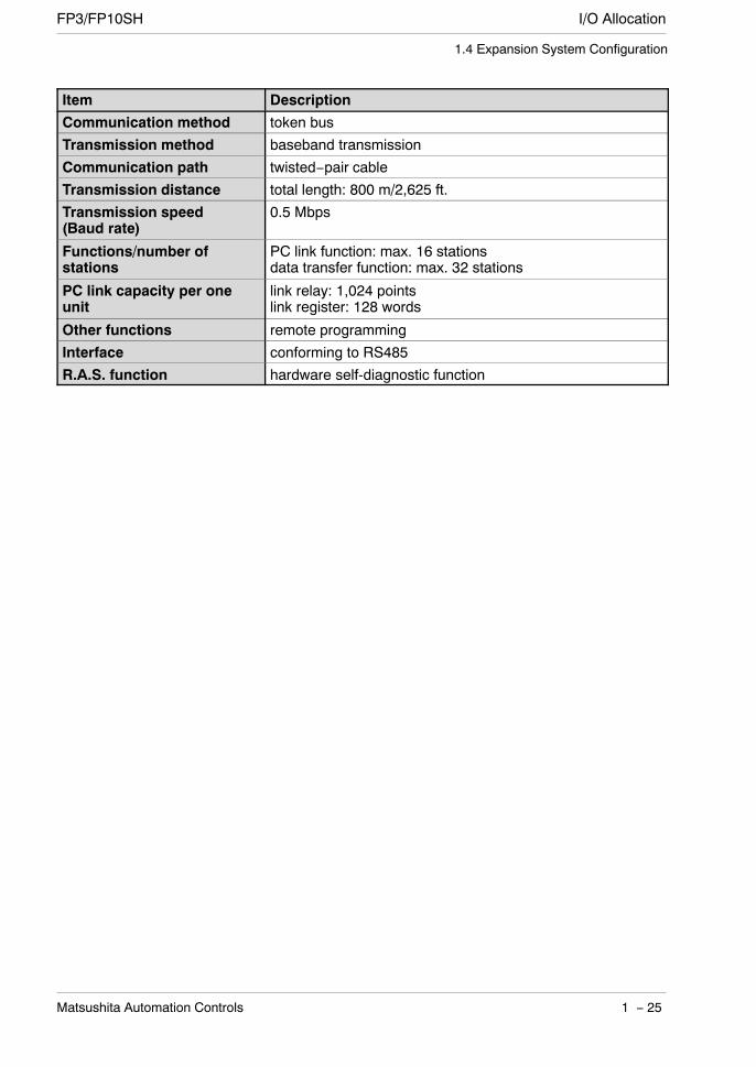
1.4 Expansion System Configuration
Item Description
Communication method token bus
Transmission method baseband transmission
Communication path twisted−pair cable
Transmission distance total length: 800 m/2,625 ft.
Transmission speed(Baud rate)
0.5 Mbps
Functions/number ofstations
PC link function: max. 16 stationsdata transfer function: max. 32 stations
PC link capacity per oneunit
link relay: 1,024 pointslink register: 128 words
Other functions remote programming
Interface conforming to RS485
R.A.S. function hardware self-diagnostic function

I/O Allocation FP3/FP10SH
1 − 26 Matsushita Automation Controls
1.4 Expansion System Configuration
1.4.4 MEWNET−P Configuration
The MEWNET−P (Optical) system links between programmable controllers andbetween programmable controller and computers with optical fiber cables.The system provides five functions: PC link, computer link, data transfer, remoteprogramming and computer−to−computer communication functions.Since it possesses loop−back functions and other RAS functions for measures againstmalfunctions, observation devices for monitoring the link system are unnecessary. Withthe use of the optical fiber cables, a highly reliable system with minimal noiseinterference can be constructed.This network is recommended for medium−sized computer link system.For more information regarding the MEWNET−P system, refer to the MEWNET−Pmanual.
Max. 63 stations/network(Max. 16 stations for PC link function)
Loop with optical fibercables:up to 800 m/2,642 ft.between stationsup to 10 km/32,808 ft.total distance
MEWNET−Plink board
PC link functionThe internal link relays (L) and data link registers (LD) are installed to share data(contact and register information) among the programmable controllers that areconnected in an MEWNET network.
Computer link functionThe host computer sends commands to the programmable controllers on network andwrites and reads the input/output information of relays as well as the data registerinformation. The communication programs are unnecessary on the programmablecontroller side.
Data transfer functionWith the F145 (SEND)/P145 (PSEND) and F146 (RECV)/P146 (PRECV) instructionsto send and receive data, you can specify the format (bit or word) and length of the datato be sent and received, and appoint a destination station or an address. It is easy toshare data among the programmable controllers on the network. The remote stationsdo not need a send/receive program.

I/O AllocationFP3/FP10SH
1 − 27Matsushita Automation Controls
1.4 Expansion System Configuration
Item Description
Communication method token ring
Transmission method baseband transmission
Communication path two−core optical fiber cable
Transmission distance between stations: 800 m/2,642 ft.total distance: 10 km/32,808 ft.
Transmission speed(Baud rate)
375 kbps
Functions/number ofstations
PC link function: max. 16 stationscomputer link function: max. 63 stationsdata transfer function: max. 63 stations
PC link capacity per oneunit
link relay: 1,024 pointslink register: 128 words
Other functions remote programmingcomputer−to−computer communication
R.A.S. function loop automatic return functionnode bypass functionself−diagnosis function(hardware and transmission system test)

I/O Allocation FP3/FP10SH
1 − 28 Matsushita Automation Controls
1.4 Expansion System Configuration
1.4.5 Computer Link Function
The FP3 can be connected to the computer as an addition to the computercommunication unit (C.C.U.). Since a RS232C port comes standard on the CPU forthe FP10SH, direct connection to and communication with the computer can beachieved without the addition of any intelligent units.Using a host computer program, the relay conditions and register contents of the CPUcan be read and written.The host computer program are created in BASIC, or other languages, based on thededicated protocol (MEWTOCOL−COM).With communications from a host computer, communication programs areunnecessary on the CPU side.For more information regarding the computer link function, refer to the C−NET link unitmanual.
1:1 communication(One computer to one FP3/FP10SHcommunication)
When using the RS232C port of FP10SHCPU
1:N communication(One computer to multiple FP3/FP10SHcommunication)
PC <FP10SH>CPU
PC <FP3>CPU C.C.U.
RS232C cable RS232C port
RS232C cable
RS232C port
When using the RS232C port of C.C.U.
PC C−NET adapter
<FP3> C.C.U.
RS232C cable
RS232C cable<FP10SH>
C−NETadapter
CPU
Two−corecables (RS485):(VCTF 0.75× 2C)
Amax.of 32stationscanbe connected.
I/O AllocationFP3/FP10SH
1 − 29Matsushita Automation Controls
1.4 Expansion System Configuration
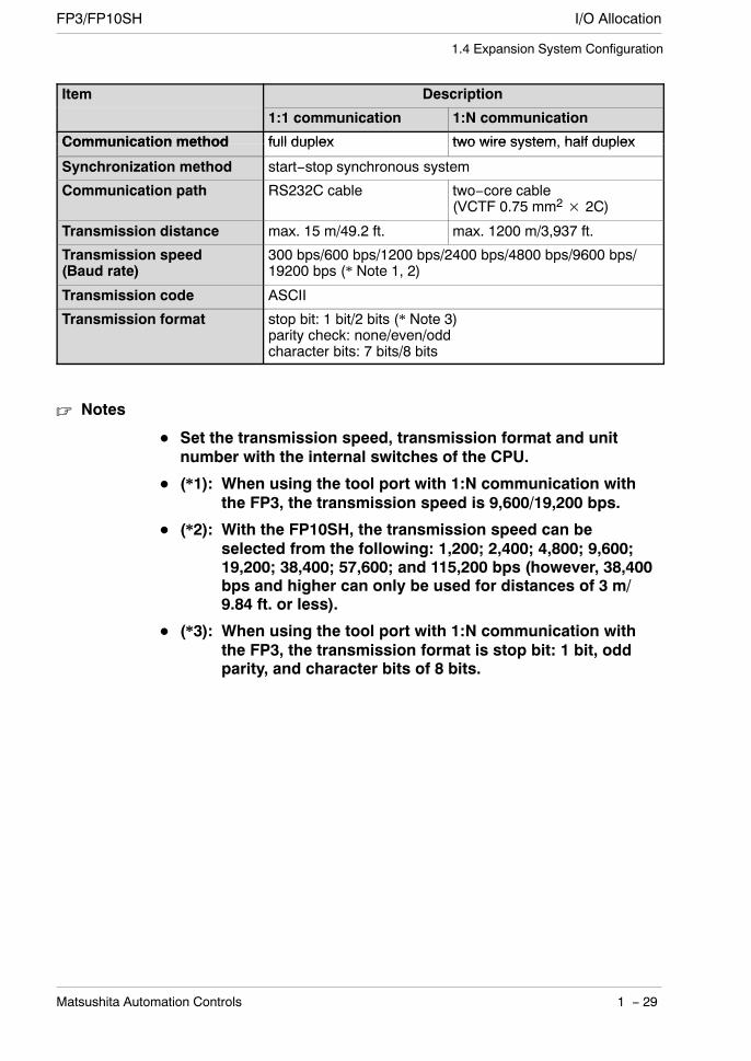
Item Description
1:1 communication 1:N communication
Communication method full duplex two wire system half duplexCommunication method full duplex two wire system, half duplex
Synchronization method start−stop synchronous system
Communication path RS232C cable two−core cable(VCTF 0.75 mm2× 2C)
Transmission distance max. 15 m/49.2 ft. max. 1200 m/3,937 ft.
Transmission speed(Baud rate)
300 bps/600 bps/1200 bps/2400 bps/4800 bps/9600 bps/19200 bps (* Note 1, 2)
Transmission code ASCII
Transmission format stop bit: 1 bit/2 bits (* Note 3)parity check: none/even/oddcharacter bits: 7 bits/8 bits
Notes
Set the transmission speed, transmission format and unitnumber with the internal switches of the CPU.
(*1): When using the tool port with 1:N communication withthe FP3, the transmission speed is 9,600/19,200 bps.
(*2): With the FP10SH, the transmission speed can beselected from the following: 1,200; 2,400; 4,800; 9,600;19,200; 38,400; 57,600; and 115,200 bps (however, 38,400bps and higher can only be used for distances of 3 m/9.84 ft. or less).
(*3): When using the tool port with 1:N communication withthe FP3, the transmission format is stop bit: 1 bit, oddparity, and character bits of 8 bits.

I/O Allocation FP3/FP10SH
1 − 30 Matsushita Automation Controls
1.4 Expansion System Configuration
1.4.6 Control by MODEM
FP3/FP10SH can be connected to MODEM for programming or computer linking overlong distances by using public telephone lines.When the power supply is turned ON, it will verify whether a MODEM is connected, and,if a MODEM is, it will automatically transmit the AT command to set the MODEM forautomatic reception.Since the reading and writing of the relay conditions and register contents of theprogrammable controller can be performed from the host computer, this function isapplicable for remote monitoring systems.When using the tool port, you can use NPST−GR software and perform reading andwriting of the programmable controller program and maintenance operations.When using the COM port (RS232C), transmission from the programmable controllerside can also be programmed.
1:1 communicationConnections to a MODEM can be madeusing either the RS232C port or theRS422 port.
When using FP10SH COM. port (RS232C)
1:N communicationUsing the C−NET adapter enablesMODEMs to be connected for multipleFP3/FP10SH.
When using FP3 CPU tool port (RS422)
MODEM
<FP10SH>
<FP3>
RS232C cableRS232C port
C−NETadapter
Two−corecables (RS485):(VCTF 0.75× 2C)
Amax.of 32stationscanbe connected.
MODEM
Publictelephone line
Publictelephone line
Publictelephone line
RS422 portRS422/232Cadapter
MODEM MODEM
C−NETadapter
C−NETadapter
MODEM MODEM
<FP3>
RS422 port
<FP10SH>
RS232C port
RS232Ccable

I/O AllocationFP3/FP10SH
1 − 31Matsushita Automation Controls
1.4 Expansion System Configuration
Item Description
FP3 FP10SH
Communication method half duplex
Synchronization method start−stop synchronous system
Transmission speed(Baud rate) (* Note)
2,400 bps (fixed) 1,200 bps/2,400 bps/4,800 bps/9,600 bps/19,200 bps/38,400 bps/57,600 bps/115,200 bps
Transmission code ASCII
Transmission format( l bi ) ( N )
Start bit: 1-bit(total: 10 bits) (* Note) Stop bit: 1-bit/2-bit
Parity check: none/odd/even
Character bit: 7-bit/8-bit
Note
Set the transmission speed and transmission format using theinternal switches of the CPU.
I/O Allocation FP3/FP10SH
1 − 32 Matsushita Automation Controls
1.5 Programming Tools
1.5 Programming Tools
1.5.1 Tools Needed for Programming
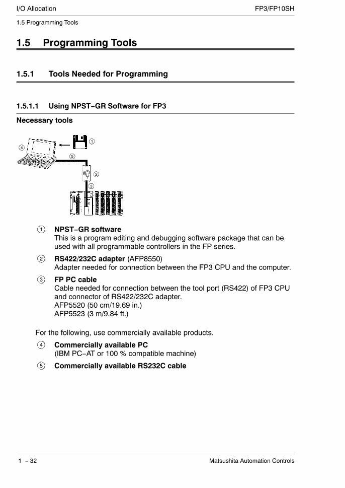
1.5.1.1 Using NPST−GR Software for FP3
Necessary tools
4
1
5
2
3
1 NPST−GR softwareThis is a program editing and debugging software package that can beused with all programmable controllers in the FP series.
2 RS422/232C adapter (AFP8550)Adapter needed for connection between the FP3 CPU and the computer.
3 FP PC cableCable needed for connection between the tool port (RS422) of FP3 CPUand connector of RS422/232C adapter.AFP5520 (50 cm/19.69 in.)AFP5523 (3 m/9.84 ft.)
For the following, use commercially available products.
4 Commercially available PC(IBM PC−AT or 100 % compatible machine)
5 Commercially available RS232C cable
I/O AllocationFP3/FP10SH
1 − 33Matsushita Automation Controls
1.5 Programming Tools
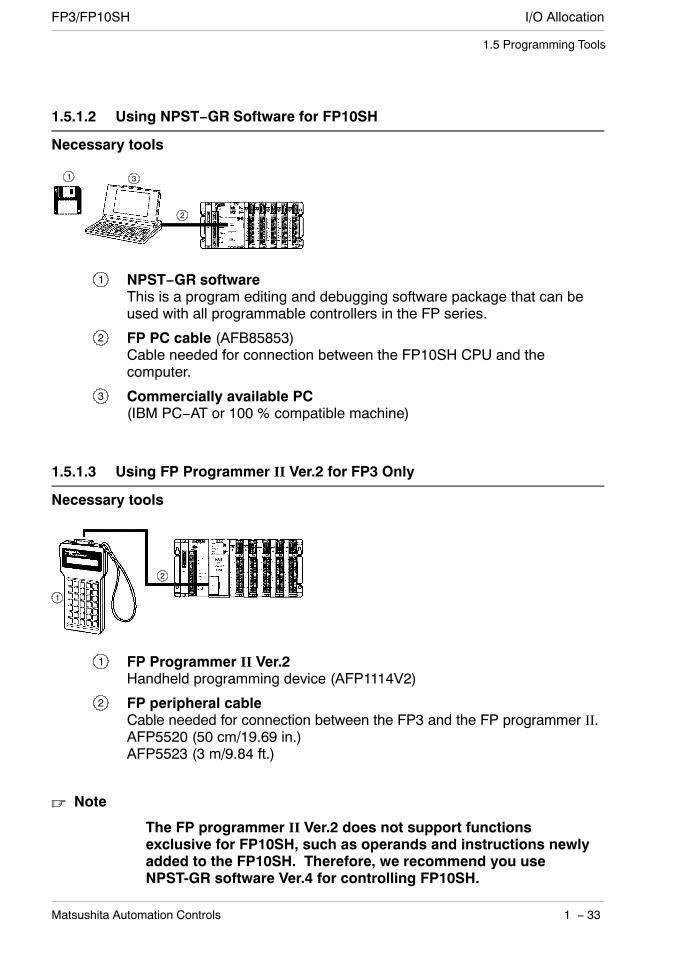
1.5.1.2 Using NPST−GR Software for FP10SH
Necessary tools
3
2
1
1 NPST−GR softwareThis is a program editing and debugging software package that can beused with all programmable controllers in the FP series.
2 FP PC cable (AFB85853)Cable needed for connection between the FP10SH CPU and thecomputer.
3 Commercially available PC(IBM PC−AT or 100 % compatible machine)
1.5.1.3 Using FP Programmer II Ver.2 for FP3 Only
Necessary tools
1
2
1 FP Programmer II Ver.2Handheld programming device (AFP1114V2)
2 FP peripheral cableCable needed for connection between the FP3 and the FP programmer II.AFP5520 (50 cm/19.69 in.)AFP5523 (3 m/9.84 ft.)
Note
The FP programmer II Ver.2 does not support functionsexclusive for FP10SH, such as operands and instructions newlyadded to the FP10SH. Therefore, we recommend you useNPST-GR software Ver.4 for controlling FP10SH.
I/O Allocation FP3/FP10SH
1 − 34 Matsushita Automation Controls
1.5 Programming Tools
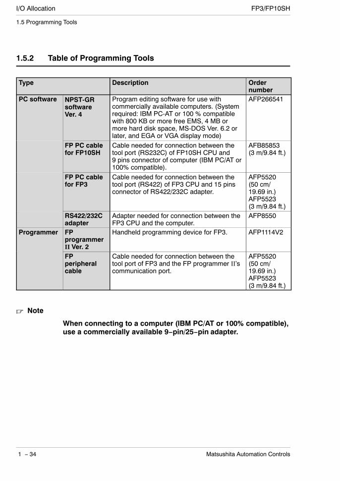
1.5.2 Table of Programming Tools
Type Description Ordernumber
PC software NPST-GRsoftwareVer. 4
Program editing software for use withcommercially available computers. (Systemrequired: IBM PC-AT or 100 % compatiblewith 800 KB or more free EMS, 4 MB ormore hard disk space, MS-DOS Ver. 6.2 orlater, and EGA or VGA display mode)
AFP266541
FP PC cablefor FP10SH
Cable needed for connection between thetool port (RS232C) of FP10SH CPU and9 pins connector of computer (IBM PC/AT or100% compatible).
AFB85853(3 m/9.84 ft.)
FP PC cablefor FP3
Cable needed for connection between thetool port (RS422) of FP3 CPU and 15 pinsconnector of RS422/232C adapter.
AFP5520(50 cm/19.69 in.)AFP5523(3 m/9.84 ft.)
RS422/232Cadapter
Adapter needed for connection between theFP3 CPU and the computer.
AFP8550
Programmer FPprogrammerII Ver. 2
Handheld programming device for FP3. AFP1114V2
FPperipheralcable
Cable needed for connection between thetool port of FP3 and the FP programmer II’scommunication port.
AFP5520(50 cm/19.69 in.)AFP5523(3 m/9.84 ft.)
Note
When connecting to a computer (IBM PC/AT or 100% compatible),use a commercially available 9−pin/25−pin adapter.
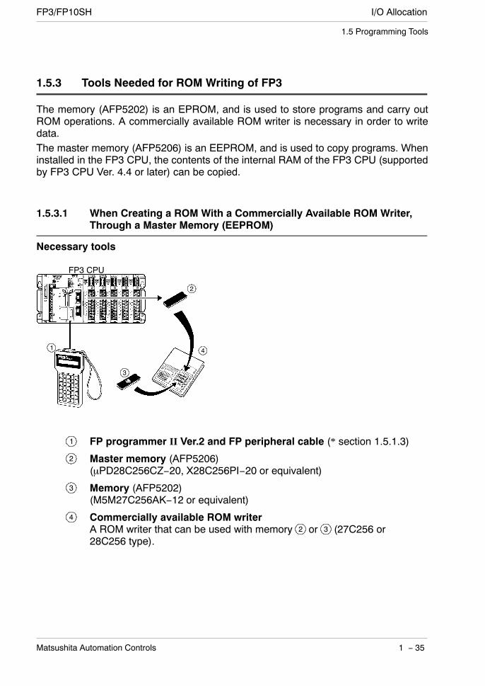
I/O AllocationFP3/FP10SH
1 − 35Matsushita Automation Controls
1.5 Programming Tools
1.5.3 Tools Needed for ROM Writing of FP3
The memory (AFP5202) is an EPROM, and is used to store programs and carry outROM operations. A commercially available ROM writer is necessary in order to writedata.The master memory (AFP5206) is an EEPROM, and is used to copy programs. Wheninstalled in the FP3 CPU, the contents of the internal RAM of the FP3 CPU (supportedby FP3 CPU Ver. 4.4 or later) can be copied.
1.5.3.1 When Creating a ROM With a Commercially Available ROM Writer,Through a Master Memory (EEPROM)
Necessary tools
3
4
2
FP3 CPU
1
1 FP programmer II Ver.2 and FP peripheral cable (* section 1.5.1.3)
2 Master memory (AFP5206)(µPD28C256CZ−20, X28C256PI−20 or equivalent)
3 Memory (AFP5202)(M5M27C256AK−12 or equivalent)
4 Commercially available ROM writerA ROM writer that can be used with memory 2 or 3 (27C256 or28C256 type).

I/O Allocation FP3/FP10SH
1 − 36 Matsushita Automation Controls
1.5 Programming Tools
1.5.3.2 When Creating a ROM With NPST−GR Software and a CommerciallyAvailable ROM Writer
Necessary tools
3
1
4
2
PC
1 PC and NPST−GR software (* section 1.5.1.1)
2 Memory (AFP5202)(M5M27C256AK−12 or equivalent)
3 Commercially available ROM writerA ROM writer that can be used with memory 2 (27C256 type).
4 Commercially available centronics cable or commercially availableRS232C cableUse a cable that conforms with the specifications of the ROM writer.

I/O AllocationFP3/FP10SH
1 − 37Matsushita Automation Controls
1.5 Programming Tools
1.5.4 Tools Needed for ROM Writing of FP10SH
The memory (AFP5209) is an EPROM, and is used to store programs and carry outROM operations. A commercially available ROM writer is necessary in order to writedata.The master memory (AFP5208) is a FROM, and is used to copy programs. Wheninstalled in the FP10SH CPU, the contents of the internal RAM of the FP10SH CPU(supported by FP10SH CPU Ver.2 or later) can be copied.
1.5.4.1 When Creating a ROM With a Commercially Available ROM Writer,Through a Master Memory (FROM)
Necessary tools
3
1
4
5
2
FP10SH CPU
PC
1 PC, NPST−GR software and cable (* section 1.5.1.2)
2 ROM operation board (AFP6208)
3 Master memory (AFP5208)(SST−29EE020−150−4C−PHor equivalent)
4 Memory (AFP5209)(M27C2001−150F1 or equivalent)
5 Commercially available ROM writerA ROM writer that can be used with memory 4 (27C2001 type).
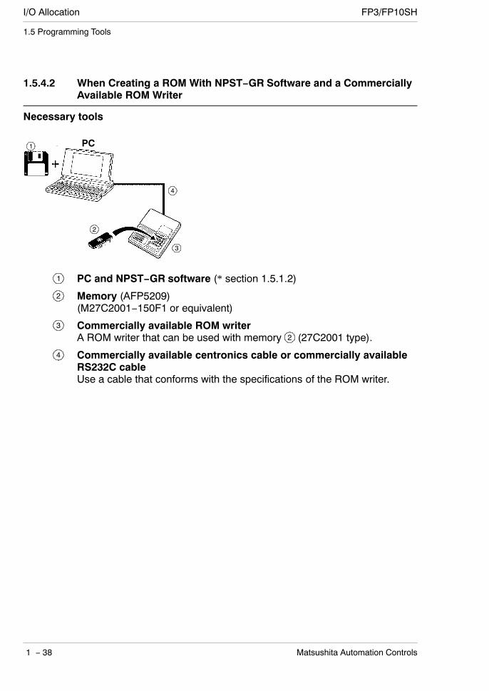
I/O Allocation FP3/FP10SH
1 − 38 Matsushita Automation Controls
1.5 Programming Tools
1.5.4.2 When Creating a ROM With NPST−GR Software and a CommerciallyAvailable ROM Writer
Necessary tools
2
1
3
4
PC
1 PC and NPST−GR software (* section 1.5.1.2)
2 Memory (AFP5209)(M27C2001−150F1 or equivalent)
3 Commercially available ROM writerA ROM writer that can be used with memory 2 (27C2001 type).
4 Commercially available centronics cable or commercially availableRS232C cableUse a cable that conforms with the specifications of the ROM writer.

Chapter 2
Parts and Its Specifications
2.1 Specifications 2 − 3. . . . . . . . . . . . . . . . . . . . . . . . . . . .
2.1.1 FP3/FP10SH General Specifications 2 − 3
2.1.2 Dimensions 2 − 3. . . . . . . . . . . . . . . . . . . . . .
2.1.3 FP3 Performance Specifications 2 − 4. . . .
2.1.4 FP10SH Performance Specifications 2 − 7
2.2 Backplane for FP3/FP10SH 2 − 10. . . . . . . . . . . . . .
2.3 Expansion Cable 2 − 12. . . . . . . . . . . . . . . . . . . . . . . .
2.4 FP3 CPU and Optional Memory 2 − 14. . . . . . . . . . .
2.4.1 FP3 CPU 2 − 14. . . . . . . . . . . . . . . . . . . . . . .
2.4.2 Memory (EPROM) and Master Memory(EEPROM) 2 − 18. . . . . . . . . . . . . . . . . . . . .
2.5 FP10SH CPU and Optional Memory 2 − 20. . . . . . .
2.5.1 FP10SH CPU 2 − 20. . . . . . . . . . . . . . . . . . .
2.5.2 Expansion Memory Unit 2 − 29. . . . . . . . . .
2.5.3 ROM Operation Board 2 − 31. . . . . . . . . . .
2.5.4 IC Memory Card Board 2 − 35. . . . . . . . . . .
2.5.5 IC Memory Card 2 − 37. . . . . . . . . . . . . . . . .
2.6 Power Supply Units 2 − 42. . . . . . . . . . . . . . . . . . . . . .
2.6.1 Power Supply Specifications 2 − 44. . . . . .
2.7 Power Supply Dummy Unit 2 − 45. . . . . . . . . . . . . . .
2.7.1 Conditions for Using a Power SupplyDummy Unit 2 − 46. . . . . . . . . . . . . . . . . . . .
2.7.2 Installing the Power Supply DummyUnit 2 − 48. . . . . . . . . . . . . . . . . . . . . . . . . . . .
next page

I/O Allocation FP3/FP10SH
2 − 2 Matsushita Automation Controls
2.8 Common Specifications of Input, Output andI/O Mixed Units 2 − 49. . . . . . . . . . . . . . . . . . . . . . . . .
2.8.1 Table of Input Unit Types 2 − 50. . . . . . . . .
2.8.2 Table of Output Unit Types 2 − 50. . . . . . . .
2.8.3 Table of I/O Mixed Unit Types 2 − 51. . . . .
2.9 Input Units Specifications 2 − 52. . . . . . . . . . . . . . . .
2.9.1 16-point Type DC Input Unit 2 − 52. . . . . . .
2.9.2 32-point Type DC Input Units 2 − 54. . . . . .
2.9.3 64-point Type DC Input Units 2 − 57. . . . . .
2.9.4 64-point/High−speed Response TypeDC Input Units 2 − 61. . . . . . . . . . . . . . . . . .
2.9.5 8-point Type AC Input Units 2 − 64. . . . . . .
2.9.6 16-point Type AC Input Units 2 − 66. . . . . .
2.10 Output Units Specifications 2 − 68. . . . . . . . . . . . . . .
2.10.1 16-point Type Relay Output Units 2 − 68. .
2.10.2 16-point Type Output Unit−TransistorNPN 2 − 70. . . . . . . . . . . . . . . . . . . . . . . . . . .
2.10.3 32-point Type Output Unit−TransistorNPN 2 − 72. . . . . . . . . . . . . . . . . . . . . . . . . . .
2.10.4 64-point Type Output Unit−TransistorNPN 2 − 74. . . . . . . . . . . . . . . . . . . . . . . . . . .
2.10.5 16-point Type Output Unit−TransistorPNP 2 − 76. . . . . . . . . . . . . . . . . . . . . . . . . . .
2.10.6 32-point type Output Unit−TransistorPNP 2 − 78. . . . . . . . . . . . . . . . . . . . . . . . . . .
2.10.7 64-point Type Output Unit−TransistorPNP 2 − 80. . . . . . . . . . . . . . . . . . . . . . . . . . .
2.10.8 16-point Type Triac Output Unit 2 − 82. . . .
2.11 I/O Mixed Units Specifications 2 − 84. . . . . . . . . . . .
2.11.1 64−point Type I/O Mixed Unit−DCInput/Transistor NPN 2 − 84. . . . . . . . . . . . .
2.11.2 64−point Type I/O Mixed Unit−DCInput/Transistor PNP 2 − 88. . . . . . . . . . . . .
2.11.3 16−point Type I/O Mixed Unit−DCInput/Relay Output 2 − 92. . . . . . . . . . . . . . .

I/O AllocationFP3/FP10SH
2 − 3Matsushita Automation Controls
2.1 Specifications
2.1 Specifications
2.1.1 FP3/FP10SH General Specifications
Item Descriptions
Ambient temperature 0 to 55 °C/32 to 131 °F
Storage temperature −20 to +70 °C/−4 to +158 °F
Ambient humidity 30 to 85 % RH (non-condensing)
Storage humidity 30 to 85 % RH (non-condensing)
Breakdown voltage 1,500 V AC for 1 minute between AC external terminal andframe ground terminal500 V AC for 1 minute between DC external terminal andframe ground terminal
Insulation resistance 100 MΩ or more (measured with a 500 V DC megger testing)between external terminal and frame ground terminal
Vibration resistance 10 to 55 Hz, 1 cycle/min: double amplitude of 0.75 mm/0.030 in., 10 min on 3 axes
Shock resistance 98 m/s2 or more, 4 times on 3 axes
Noise immunity 1,500 Vp-p with pulse widths 50 ns and 1 μs(based on in-house measurements)
Operating conditions Free from corrosive gases and excessive dust
2.1.2 Dimensions
Master backplane Expansion backplaneAB
150/5.906
120/4.724
100/3.937
(unit: mm/in.)
AB
150/5.906
120/4.724
100/3.937
(unit: mm/in.)
Type A (mm/in.): Overall length B (mm/in.): Mounting hole pitch3-slot type 260/10.236 245/9.6465-slot type 330/12.992 315/12.4028-slot type 435/17.126 420/16.535
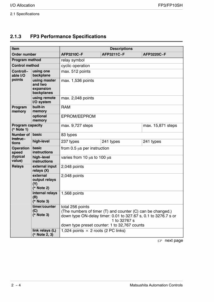
I/O Allocation FP3/FP10SH
2 − 4 Matsushita Automation Controls
2.1 Specifications
2.1.3 FP3 Performance Specifications
Item Descriptions
Order number AFP3210C−F AFP3211C−F AFP3220C−FProgram method relay symbolControl method cyclic operationControll−able I/O
using onebackplane
max. 512 pointsable I/Opoints using master
and twoexpansionbackplanes
max. 1,536 points
using remoteI/O system
max. 2,048 points
Programmemory
built-inmemory
RAMe o y
optionalmemory
EPROM/EEPROM
Program capacity(* Note 1)
max. 9,727 steps max. 15,871 steps
Number ofinstruc−
basic 83 typesinstruc−tions high-level 237 types 241 types 241 types
Operationspeed
basicinstructions
from 0.5 μs per instructionspeed(typicalvalue)
high−levelinstructions
varies from 10 μs to 100 μs
Relays external inputrelays (X)
2,048 points
externaloutput relays(Y)(* Note 2)
2,048 points
internal relays(R)(* Note 3)
1,568 points
timer/counter(C)(* Note 3)
total 256 points(The numbers of timer (T) and counter (C) can be changed.)down type ON-delay timer: 0.01 to 327.67 s, 0.1 to 3276.7 s or
1 to 32767 sdown type preset counter: 1 to 32,767 counts
link relays (L)(* Note 2, 3)
1,024 points× 2 roots (2 PC links)
next page

I/O AllocationFP3/FP10SH
2 − 5Matsushita Automation Controls
2.1 Specifications
Item Descriptions
Order number AFP3210C−F AFP3211C−F AFP3220C−FMemoryareas
data registers(DT)(* Note 3)
2,048 words
File registers(FL)(* Note 1, 3)
0 to 8,192 words 8,192 to 22,525words
link dataregisters (LD)(* Note 3, 4)
128 words× 2 roots (2 PC links)
timer/counterset value area(SV)
256 words
timer/counterelapsed valuearea (EV)
256 words
indexregisters(IX, IY)
2 words
Differential points(DF and DF/)
unlimited number of points
Auxiliary timer unlimited number of points, down type timer (0.01 to 327.67 s)Master control relaypoints (MCR)
64 points
Number of labels(JP and LOOP)
256 labels
Number of step ladder(* Note 3)
1,000 stages
Number of subroutine 100 subroutinesNumber of interruptprogram
25 programs
Comment input function(* Note 5)
not available available not available
Sampling trace function(* Note 6)
not available available available
Clock/calendar function year, month, day, hour, minute, second and day of weekLink functions PC link, computer link, data transfer, remote programming and
MODEM capabilitySelf-diagnostic function watching dog timer, memory malfunction detection, I/O
malfunction detection, backup battery malfunction detection,program syntax check, etc.
Other functions program edition during RUN (* Note 7), forced ON/OFF, interruptinput, test run, constant scan and machine language programoption
Memory backup time(lithium battery storagetime)
AFP3210C−F : min. 17,000 hours(typical value : approx. 34,000 hours)
AFP3211C−F, AFP3220C−F : min. 10,000 hours(typical value : approx. 22,000hours)
next page
I/O Allocation FP3/FP10SH
2 − 6 Matsushita Automation Controls
2.1 Specifications
Notes
(*1): The capacity will differ depending on the system registersettings.
(*2): Can also be used as an internal relay.
(*3): Hold or non−hold type can be set.
(*4): Can also be used as a data register.
(*5): Max. 2,730 points. Up to 12 characters per 1 comment.
(*6): Can perform sampling up to a maximum of 1,000samples (4,000 words) for data of 16 contacts and 3words.
(*7): During the ladder symbol input of NPST−GR, programedits during RUN cannot be performed.

I/O AllocationFP3/FP10SH
2 − 7Matsushita Automation Controls
2.1 Specifications
2.1.4 FP10SH Performance Specifications
Item DescriptionsOrder number AFP6221V3 AFP6211V3Program method relay symbolControl method cyclic operationControll−able I/O
using onebackplane
max. 512 pointsble I/Opoints using master
and threeexpansionbackplanes
max. 2,048 points
using remoteI/O system
max. 8,192 points
Programmemory
built-inmemory
RAMe o y
Optionalmemory
IC memory card (* Note 4) or EPROM/FROM (* Note 5)
Program capacity approx. 30 k steps (Approx. 60 k or 120 k steps available byinstalling optional expansion memory.)
Number ofinstruc−
basic 95 typesinstruc−tions high-level 431 types
Operationspeed
basicinstructions
from 40 ns per instruction from 100 ns per instructionspeed(typicalvalue)
high−levelinstructions
from 80 ns per instruction from 200 ns per instruction
Relays external inputrelays (X)
8,192 points
externaloutput relays(Y) (* Note 1)
8,192 points
internal relays(R)(* Note 2)
14,192 points
timer/counter(* Note 2)
total 3,072 points(TM number of timer (T) and counter (C) can be changed.)− down type ON-delay timer: 0.001 to 32.767 s, 0.01 to 327.67 s,
0.1 to 3276.7 s or 1 to 32,767 s− down type preset counter: 1 to 32,767 counts
link relays (L)(* Note 1, 2)
10,240 points
pulse relays(P)(* Note 1, 2)
2,048 points
alarm relays(E)(* Note 1, 2)
2,048 points
next page

I/O Allocation FP3/FP10SH
2 − 8 Matsushita Automation Controls
2.1 Specifications
Item Descriptions
Order number AFP6221V3 AFP6211V3Memoryareas
data registers(DT) (* Note 2)
10,240 words
file registers(FL) (* Note 2)
32,765 words
link dataregisters (LD)(* Note 2, 3)
8,448 words
timer/counterset value area(SV)
3,072 words
timer/counterelapsed valuearea (EV)
3,072 words
indexregisters(I)
14 words (I0 to ID) (with bank switching, 224 words portions canbe used)
Differential points(DF and DF/)
unlimited number of points
Auxiliary timer unlimited number of points, down type timer (0.01 to 327.67 s)Master control relaypoints (MCR)
256 points (when using the 90 k step expansion memory, up to atotal of 512 points can be used for the no. 1 and 2 programs)
Number of labels(JP and LOOP)
256 points (when using the 90 k step expansion memory, up to atotal of 512 points can be used for the no. 1 and 2 programs)
Number of step ladder(* Note 2)
1,000 steps (can only be used for the no. 1 program)
Number of subroutine 100 subroutines (can only be used for the no. 1 program)Number of interruptprogram
25 program (can only be used for the no. 1 program)
Comment input function available (either the IC memory card board or ROM operationboard are required)
Sampling trace function max. 1,000 samples (16 contacts and 3 words/sample)Clock/calendar function year, month, day, hour, minute, second and day of weekLink functions PC link, computer link, data transfer, remote programming and
MODEM capabilitySelf-diagnostic function watching dog timer, memory malfunction detection, I/O malfunction
detection, backup battery malfunction detection, program syntaxcheck, etc.
Other functions program edition during RUN, forced ON/OFF, interrupt input, testrun and constant scan
Memorybackuptime
CPU only min. 4,800 hours(typical : approx. 29,000 hours)
min. 9,500 hours(typical : approx. 57,000 hours)
time(lithiumbatterystoragetime)
when usedexpansionmemory
min. 4,300 hours (* Note 6)(typical : approx. 25,000 hours)
min. 7,600 hours (* Note 6)(typical : approx. 44,000 hours)
next page
I/O AllocationFP3/FP10SH
2 − 9Matsushita Automation Controls
2.1 Specifications
Notes
(*1): Can also be used as an internal relay.
(*2): Hold or non−hold type can be set.
(*3): Can also be used as a data register.
(*4): In addition to the IC memory card, the IC memory cardboard (AFP6209A) is required.
(*5): In addition to the ROM, the ROM operation board(AFP6208) is required.
(*6): The value when the 90 k steps type expansion memoryboard (AFP6205) is used.
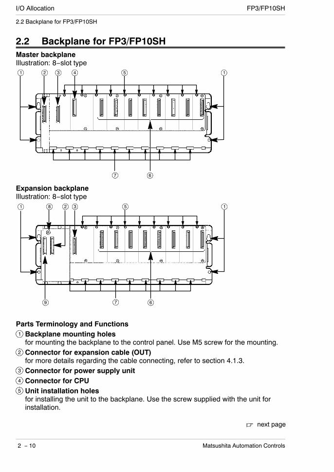
I/O Allocation FP3/FP10SH
2 − 10 Matsushita Automation Controls
2.2 Backplane for FP3/FP10SH
2.2 Backplane for FP3/FP10SHMaster backplaneIllustration: 8−slot type
32 4
67
1 5 1
Expansion backplaneIllustration: 8−slot type
2
9 67
1 58 3 1
Parts Terminology and Functions1 Backplane mounting holesfor mounting the backplane to the control panel. Use M5 screw for the mounting.
2 Connector for expansion cable (OUT)for more details regarding the cable connecting, refer to section 4.1.3.
3 Connector for power supply unit4 Connector for CPU5 Unit installation holesfor installing the unit to the backplane. Use the screw supplied with the unit forinstallation.
next page
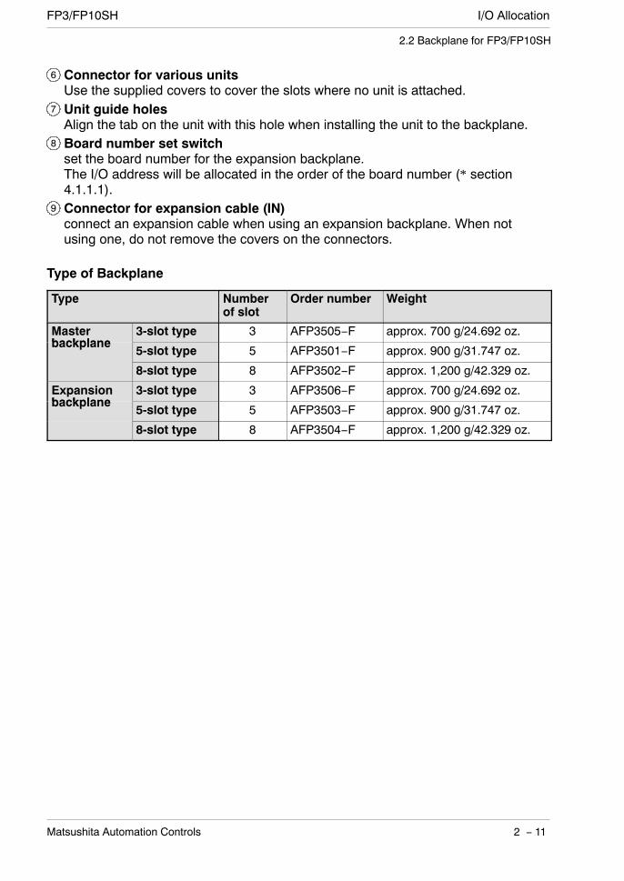
I/O AllocationFP3/FP10SH
2 − 11Matsushita Automation Controls
2.2 Backplane for FP3/FP10SH
6 Connector for various unitsUse the supplied covers to cover the slots where no unit is attached.
7 Unit guide holesAlign the tab on the unit with this hole when installing the unit to the backplane.
8 Board number set switchset the board number for the expansion backplane.The I/O address will be allocated in the order of the board number (* section4.1.1.1).
9 Connector for expansion cable (IN)connect an expansion cable when using an expansion backplane. When notusing one, do not remove the covers on the connectors.
Type of Backplane
Type Numberof slot
Order number Weight
Masterbackplane
3-slot type 3 AFP3505−F approx. 700 g/24.692 oz.backplane
5-slot type 5 AFP3501−F approx. 900 g/31.747 oz.
8-slot type 8 AFP3502−F approx. 1,200 g/42.329 oz.
Expansionbackplane
3-slot type 3 AFP3506−F approx. 700 g/24.692 oz.backplane
5-slot type 5 AFP3503−F approx. 900 g/31.747 oz.
8-slot type 8 AFP3504−F approx. 1,200 g/42.329 oz.
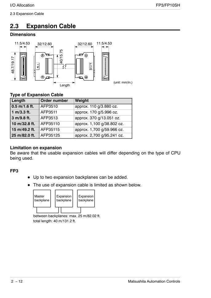
I/O Allocation FP3/FP10SH
2 − 12 Matsushita Automation Controls
2.3 Expansion Cable
2.3 Expansion CableDimensions
Length(unit: mm/in.)
48.7/19.17
40/15.75
11.5/4.53 32/12.60 32/12.60 11.5/4.53
Type of Expansion CableLength Order number Weight0.5 m/1.6 ft. AFP3510 approx. 110 g/3.880 oz.1 m/3.3 ft. AFP3511 approx. 170 g/5.996 oz.3 m/9.8 ft. AFP3513 approx. 370 g/13.051 oz.10 m/32.8 ft. AFP35110 approx. 1,100 g/38.802 oz.15 m/49.2 ft. AFP35115 approx. 1,700 g/59.966 oz.25 m/82.0 ft. AFP35125 approx. 2,700 g/95.241 oz.
Limitation on expansionBe aware that the usable expansion cables will differ depending on the type of CPUbeing used.
FP3Up to two expansion backplanes can be added.
The use of expansion cable is limited as shown below.
Masterbackplane
Expansionbackplane
between backplanes: max. 25 m/82.02 ft.total length: 40 m/131.2 ft.
Expansionbackplane
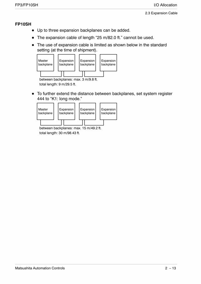
I/O AllocationFP3/FP10SH
2 − 13Matsushita Automation Controls
2.3 Expansion Cable
FP10SHUp to three expansion backplanes can be added.
The expansion cable of length “25 m/82.0 ft.” cannot be used.
The use of expansion cable is limited as shown below in the standardsetting (at the time of shipment).
between backplanes: max. 3 m/9.8 ft.total length: 9 m/29.5 ft.
Masterbackplane
Expansionbackplane
Expansionbackplane
Expansionbackplane
To further extend the distance between backplanes, set system register444 to “K1: long mode.”
between backplanes: max. 15 m/49.2 ft.total length: 30 m/98.43 ft.
Masterbackplane
Expansionbackplane
Expansionbackplane
Expansionbackplane

I/O Allocation FP3/FP10SH
2 − 14 Matsushita Automation Controls
2.4 FP3 CPU and Optional Memory
2.4 FP3 CPU and Optional Memory
2.4.1 FP3 CPU
1 2
3
5 6
74
8
9
Parts Terminology and Functions1 Status indicator LEDsdisplay the operating condition and error statuses (* section 2.4.1.1).
2 Initialize/test switchis used to clear the errors, initializes the operation memory and set the testoperation mode (* section 2.4.1.2).
3 Mode selectoris used to change the operation mode (* section 2.4.1.3).
4 Backup batteryfor backup of the internal memory (RAM). Not connected when the instrument isdelivered.
5 Memory protect and baud rate selectoris used to select the writing operation for the program memory and to set thebaud rate for the tool port.
Switch ItemSwitch positionSwitch
number ItemON OFF
1 Program memory protection switch Write protected Write enabled
2 Baud rate selector for tool port 9600 bps 19200 bps
next page
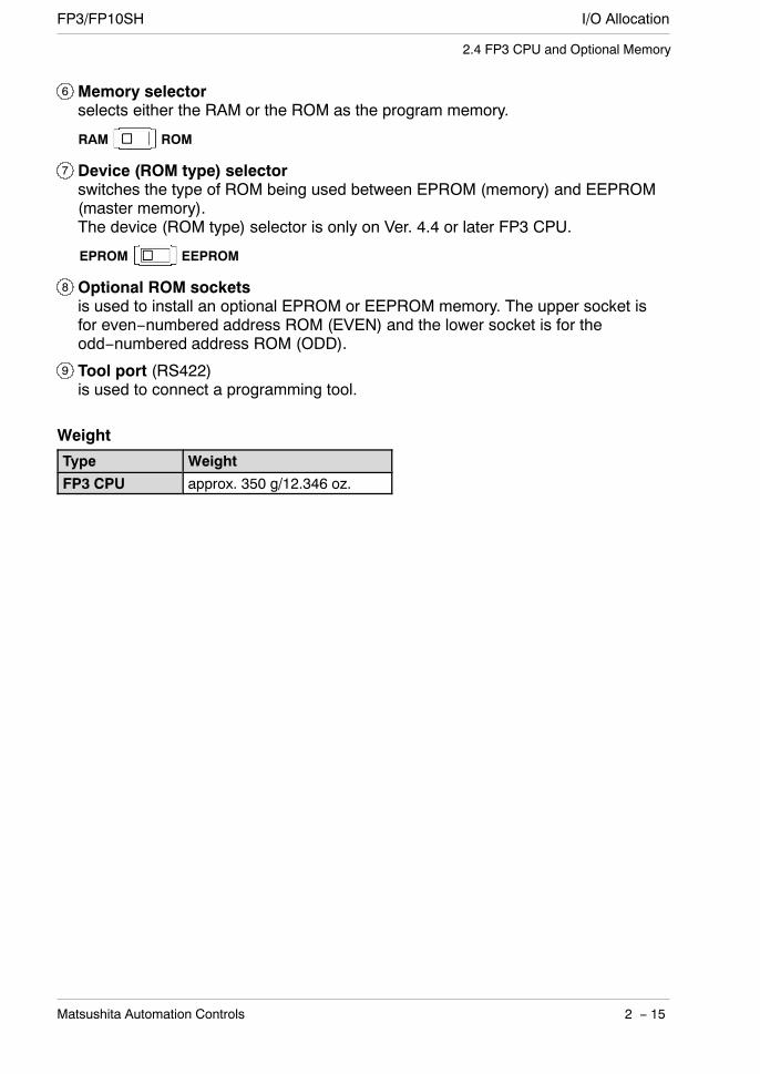
I/O AllocationFP3/FP10SH
2 − 15Matsushita Automation Controls
2.4 FP3 CPU and Optional Memory
6 Memory selectorselects either the RAM or the ROM as the program memory.
RAM ROM
7 Device (ROM type) selectorswitches the type of ROM being used between EPROM (memory) and EEPROM(master memory).The device (ROM type) selector is only on Ver. 4.4 or later FP3 CPU.
EPROM EEPROM
8 Optional ROM socketsis used to install an optional EPROM or EEPROM memory. The upper socket isfor even−numbered address ROM (EVEN) and the lower socket is for theodd−numbered address ROM (ODD).
9 Tool port (RS422)is used to connect a programming tool.
Weight
Type Weight
FP3 CPU approx. 350 g/12.346 oz.
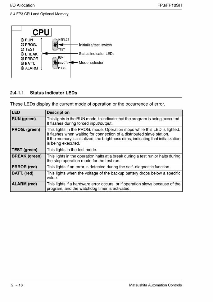
I/O Allocation FP3/FP10SH
2 − 16 Matsushita Automation Controls
2.4 FP3 CPU and Optional Memory
Status indicator LEDs
Mode selector
Initialize/test switch
2.4.1.1 Status Indicator LEDs
These LEDs display the current mode of operation or the occurrence of error.
LED Description
RUN (green) This lights in theRUNmode, to indicate that the program is being executed.It flashes during forced input/output.
PROG. (green) This lights in the PROG. mode. Operation stops while this LED is lighted.It flashes when waiting for connection of a distributed slave station.If the memory is initialized, the brightness dims, indicating that initializationis being executed.
TEST (green) This lights in the test mode.
BREAK (green) This lights in the operation halts at a break during a test run or halts duringthe step operation mode for the test run.
ERROR (red) This lights if an error is detected during the self−diagnostic function.
BATT. (red) This lights when the voltage of the backup battery drops below a specificvalue.
ALARM (red) This lights if a hardware error occurs, or if operation slows because of theprogram, and the watchdog timer is activated.
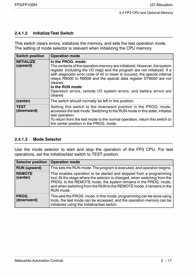
I/O AllocationFP3/FP10SH
2 − 17Matsushita Automation Controls
2.4 FP3 CPU and Optional Memory
2.4.1.2 Initialize/Test Switch
This switch clears errors, initializes the memory, and sets the test operation mode.The setting of mode selector is relevant when initializing the CPU memory.
Switch position Operation mode
INITIALIZE(upward)
In the PROG. mode:The contents of the operationmemory are initialized.However, the systemregister (including the I/O map) and the program are not initialized. If aself−diagnostic error code of 42 or lower is occured, the special internalrelays R9000 to R9008 and the special data register DT9000 are notcleared.In the RUN mode:Operation errors, remote I/O system errors, and battery errors arecleared.
(center) The switch should normally be left in this position.
TEST(downward)
Setting this switch to the downward position in the PROG. mode,accesses the test mode. Switching to the RUNmode in this state, initiatestest operation.To return from the test mode to the normal operation, return this switch tothe center position in the PROG. mode.
2.4.1.3 Mode Selector
Use the mode selector to start and stop the operation of the FP3 CPU. For testoperations, set the initialize/test switch to TEST position.
Selector position Operation mode
RUN (upward) This sets the RUNmode. The program is executed, and operation begins.
REMOTE(center)
This enables operation to be started and stopped from a programmingtool. At the stage where the selector is changed, when switching from thePROG. to the REMOTE mode, the system remains in the PROG. mode,and when switching from theRUN to the REMOTEmode, it remains in theRUN mode.
PROG.(downward)
This sets the PROG.mode. In thismode, programming can be done usingtools, the test mode can be accessed, and the operation memory can beinitialized using the Initialize/tset switch.
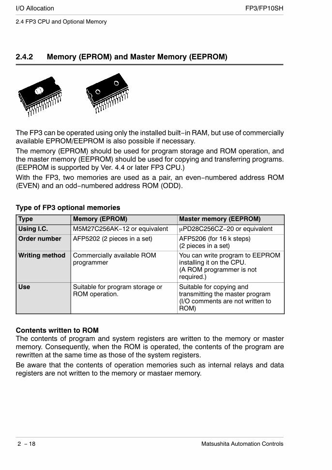
I/O Allocation FP3/FP10SH
2 − 18 Matsushita Automation Controls
2.4 FP3 CPU and Optional Memory
2.4.2 Memory (EPROM) and Master Memory (EEPROM)
The FP3 can be operated using only the installed built−in RAM, but use of commerciallyavailable EPROM/EEPROM is also possible if necessary.The memory (EPROM) should be used for program storage and ROM operation, andthe master memory (EEPROM) should be used for copying and transferring programs.(EEPROM is supported by Ver. 4.4 or later FP3 CPU.)With the FP3, two memories are used as a pair, an even−numbered address ROM(EVEN) and an odd−numbered address ROM (ODD).
Type of FP3 optional memories
Type Memory (EPROM) Master memory (EEPROM)
Using I.C. M5M27C256AK−12 or equivalent µPD28C256CZ−20 or equivalent
Order number AFP5202 (2 pieces in a set) AFP5206 (for 16 k steps)(2 pieces in a set)
Writing method Commercially available ROMprogrammer
You can write program to EEPROMinstalling it on the CPU.(A ROM programmer is notrequired.)
Use Suitable for program storage orROM operation.
Suitable for copying andtransmitting the master program(I/O comments are not written toROM)
Contents written to ROMThe contents of program and system registers are written to the memory or mastermemory. Consequently, when the ROM is operated, the contents of the program arerewritten at the same time as those of the system registers.Be aware that the contents of operation memories such as internal relays and dataregisters are not written to the memory or mastaer memory.
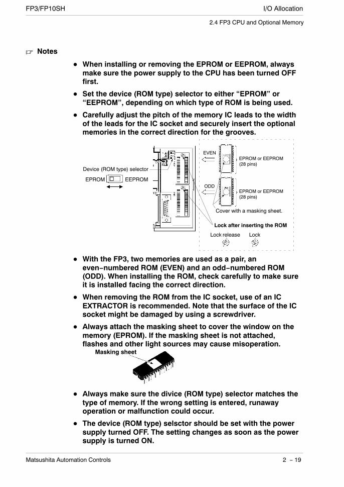
I/O AllocationFP3/FP10SH
2 − 19Matsushita Automation Controls
2.4 FP3 CPU and Optional Memory
Notes
When installing or removing the EPROM or EEPROM, alwaysmake sure the power supply to the CPU has been turned OFFfirst.
Set the device (ROM type) selector to either “EPROM” or“EEPROM”, depending on which type of ROM is being used.
Carefully adjust the pitch of the memory IC leads to the widthof the leads for the IC socket and securely insert the optionalmemories in the correct direction for the grooves.
EPROM EEPROM
Device (ROM type) selector
Cover with a masking sheet.
Lock after inserting the ROM
EPROM or EEPROM(28 pins)
EPROM or EEPROM(28 pins)
EVEN
ODD
Lock release Lock
With the FP3, two memories are used as a pair, aneven−numbered ROM (EVEN) and an odd−numbered ROM(ODD). When installing the ROM, check carefully to make sureit is installed facing the correct direction.
When removing the ROM from the IC socket, use of an ICEXTRACTOR is recommended. Note that the surface of the ICsocket might be damaged by using a screwdriver.
Always attach the masking sheet to cover the window on thememory (EPROM). If the masking sheet is not attached,flashes and other light sources may cause misoperation.
Masking sheet
Always make sure the divice (ROM type) selector matches thetype of memory. If the wrong setting is entered, runawayoperation or malfunction could occur.
The device (ROM type) selsctor should be set with the powersupply turned OFF. The setting changes as soon as the powersupply is turned ON.

I/O Allocation FP3/FP10SH
2 − 20 Matsushita Automation Controls
2.5 FP10SH CPU and Optional Memory
2.5 FP10SH CPU and Optional Memory
2.5.1 FP10SH CPU
51 2
3
8
6
4
9
7
1 Status indicator LEDsdisplay the operating condition and error statuses (* section 2.5.1.1).
2 Initialize/test switchis used to clear the errors, initializes the operation memory and set the testoperation mode (* section 2.5.1.2).
3 Mode selectoris used to change the operation mode (* section 2.5.1.3).
4 Operation condition switchesare used to set the baud rate of the programming tool, to select the programmemory, to select the writing operation for the program memory, and to set thetransmission format for the COM port (* section 2.5.1.4).
5 Station number setting switchesare used to set the station numbers (UNIT No.) for the computer link function ofthe tool port and the COM port (* section 2.5.1.5).
6 Backup batteryfor backup of the internal memory (RAM). Not connected when the instrument isdelivered.
next page
I/O AllocationFP3/FP10SH
2 − 21Matsushita Automation Controls
2.5 FP10SH CPU and Optional Memory
7 Tool port (RS232C)is used to connect a programming tool.
8 Option slotis used when installing an optional IC memory card board or a ROM operationboard.
9 COM port (RS232C)is used to connect a computer or other devices with RS232C port (* section2.5.1.6).
Weight
Type Weight
FP10SH CPU approx. 350 g/12.346 oz.
Expansionmemory unit
approx. 30 g/1.058 oz.
IC memory cardboard
approx. 60 g/2.116 oz.
ROM operationboard
approx. 35 g/1.235 oz.

I/O Allocation FP3/FP10SH
2 − 22 Matsushita Automation Controls
2.5 FP10SH CPU and Optional Memory
Status indicator LEDs
Mode selector
Initialize/test switch
2.5.1.1 Status Indicator LEDs
These LEDs display the current mode of operation or the occurrence of error.
LED Description
RUN (green) This lights in theRUNmode, to indicate that the program is being executed.It flashes during forced input/output.
PROG. (green) This lights in the PROG. mode. Operation stops while this LED is lighted.It flashes when waiting for connection of a distributed slave station.If the memory is initialized, the brightness dims, indicating that initializationis being executed.
TEST (green) This lights in the test mode.
BREAK (green) This lights in the operation halts at a break during a test run or halts duringthe step operation mode for the test run.
ERROR (red) This lights if an error is detected during the self−diagnostic function.
BATT. (red) This lights when the voltage of the backup battery drops below a specificvalue.
ALARM (red) This lights if a hardware error occurs, or if operation slows because of theprogram, and the watchdog timer is activated.
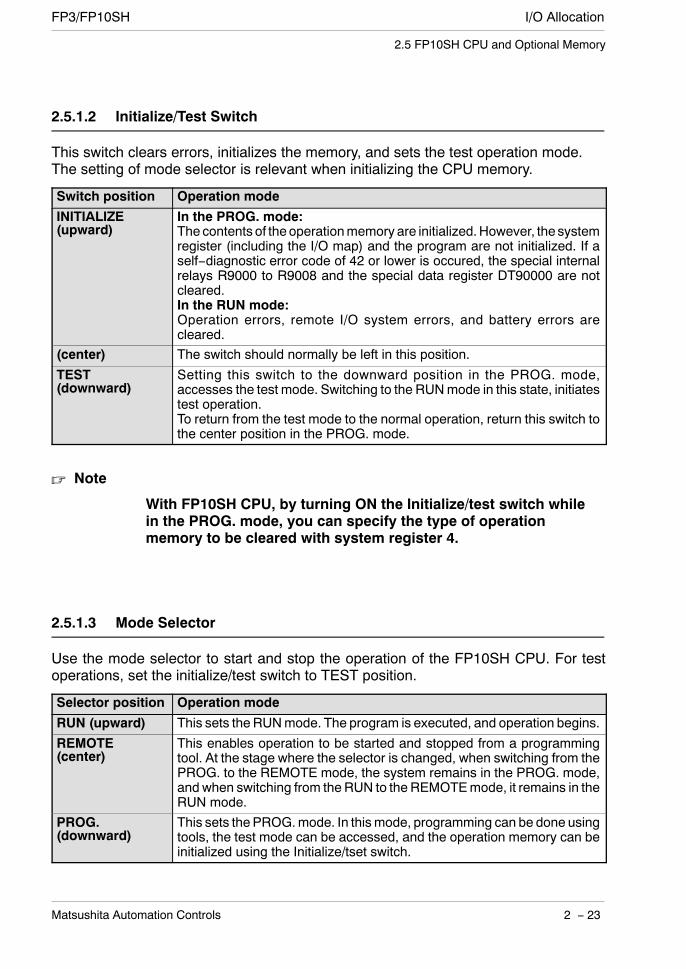
I/O AllocationFP3/FP10SH
2 − 23Matsushita Automation Controls
2.5 FP10SH CPU and Optional Memory
2.5.1.2 Initialize/Test Switch
This switch clears errors, initializes the memory, and sets the test operation mode.The setting of mode selector is relevant when initializing the CPU memory.
Switch position Operation mode
INITIALIZE(upward)
In the PROG. mode:The contents of the operationmemory are initialized.However, the systemregister (including the I/O map) and the program are not initialized. If aself−diagnostic error code of 42 or lower is occured, the special internalrelays R9000 to R9008 and the special data register DT90000 are notcleared.In the RUN mode:Operation errors, remote I/O system errors, and battery errors arecleared.
(center) The switch should normally be left in this position.
TEST(downward)
Setting this switch to the downward position in the PROG. mode,accesses the test mode. Switching to the RUNmode in this state, initiatestest operation.To return from the test mode to the normal operation, return this switch tothe center position in the PROG. mode.
Note
With FP10SH CPU, by turning ON the Initialize/test switch whilein the PROG. mode, you can specify the type of operationmemory to be cleared with system register 4.
2.5.1.3 Mode Selector
Use the mode selector to start and stop the operation of the FP10SH CPU. For testoperations, set the initialize/test switch to TEST position.
Selector position Operation mode
RUN (upward) This sets the RUNmode. The program is executed, and operation begins.
REMOTE(center)
This enables operation to be started and stopped from a programmingtool. At the stage where the selector is changed, when switching from thePROG. to the REMOTE mode, the system remains in the PROG. mode,and when switching from theRUN to the REMOTEmode, it remains in theRUN mode.
PROG.(downward)
This sets the PROG.mode. In thismode, programming can be done usingtools, the test mode can be accessed, and the operation memory can beinitialized using the Initialize/tset switch.
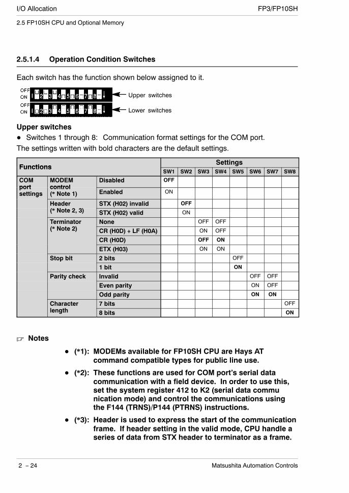
I/O Allocation FP3/FP10SH
2 − 24 Matsushita Automation Controls
2.5 FP10SH CPU and Optional Memory
2.5.1.4 Operation Condition Switches
Each switch has the function shown below assigned to it.
Upper switches
Lower switches
Upper switchesSwitches 1 through 8: Communication format settings for the COM port.
The settings written with bold characters are the default settings.
FunctionsSettings
FunctionsSW1 SW2 SW3 SW4 SW5 SW6 SW7 SW8
COMport
MODEMcontrol
Disabled OFFportsettings
control(* Note 1) Enabled ONg
Header(* N 2 3)
STX (H02) invalid OFF(* Note 2, 3) STX (H02) valid ON
Terminator(* N 2)
None OFF OFF(* Note 2) CR (H0D) + LF (H0A) ON OFF
CR (H0D) OFF ON
ETX (H03) ON ON
Stop bit 2 bits OFFp1 bit ON
Parity check Invalid OFF OFFyEven parity ON OFF
Odd parity ON ON
Characterl h
7 bits OFFlength 8 bits ON
Notes
(*1): MODEMs available for FP10SH CPU are Hays ATcommand compatible types for public line use.
(*2): These functions are used for COM port’s serial datacommunication with a field device. In order to use this,set the system register 412 to K2 (serial data communication mode) and control the communications usingthe F144 (TRNS)/P144 (PTRNS) instructions.
(*3): Header is used to express the start of the communicationframe. If header setting in the valid mode, CPU handle aseries of data from STX header to terminator as a frame.
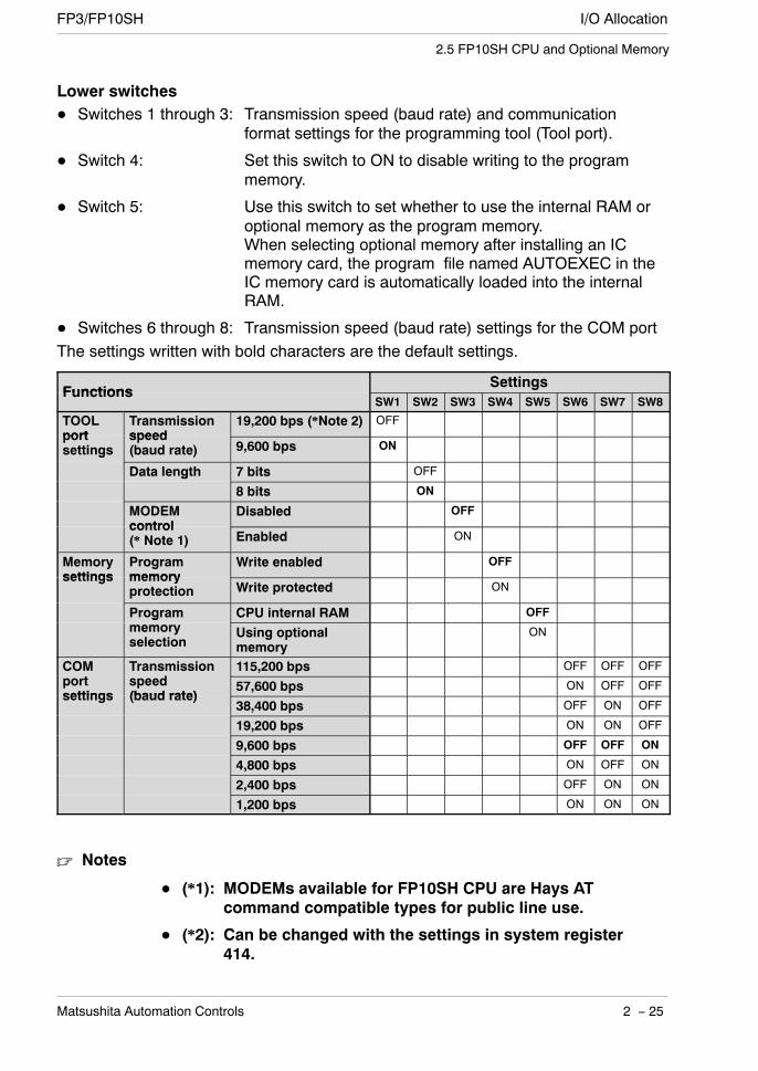
I/O AllocationFP3/FP10SH
2 − 25Matsushita Automation Controls
2.5 FP10SH CPU and Optional Memory
Lower switchesSwitches 1 through 3: Transmission speed (baud rate) and communication
format settings for the programming tool (Tool port).
Switch 4: Set this switch to ON to disable writing to the programmemory.
Switch 5: Use this switch to set whether to use the internal RAM oroptional memory as the program memory.When selecting optional memory after installing an ICmemory card, the program file named AUTOEXEC in theIC memory card is automatically loaded into the internalRAM.
Switches 6 through 8: Transmission speed (baud rate) settings for the COM portThe settings written with bold characters are the default settings.
FunctionsSettings
FunctionsSW1 SW2 SW3 SW4 SW5 SW6 SW7 SW8
TOOLport
Transmissionspeed
19,200 bps (*Note 2) OFFportsettings
speed(baud rate) 9,600 bps ONg
Data length 7 bits OFFg8 bits ON
MODEMcontrol
Disabled OFFcontrol(* Note 1) Enabled ON
Memorysettings
Programmemory
Write enabled OFFsettings memory
protection Write protected ON
Program CPU internal RAM OFFgmemoryselection
Using optionalmemory
ON
COM Transmissiond
115,200 bps OFF OFF OFFportsettings
speed(baud rate)
57,600 bps ON OFF OFFsettings (baud rate)
38,400 bps OFF ON OFF
19,200 bps ON ON OFF
9,600 bps OFF OFF ON
4,800 bps ON OFF ON
2,400 bps OFF ON ON
1,200 bps ON ON ON
Notes
(*1): MODEMs available for FP10SH CPU are Hays ATcommand compatible types for public line use.
(*2): Can be changed with the settings in system register414.
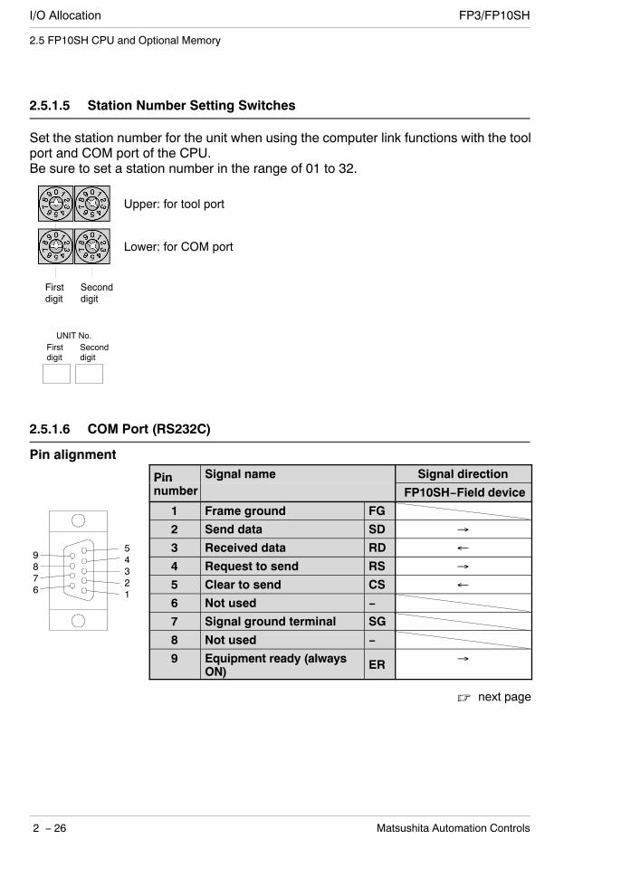
I/O Allocation FP3/FP10SH
2 − 26 Matsushita Automation Controls
2.5 FP10SH CPU and Optional Memory
2.5.1.5 Station Number Setting Switches
Set the station number for the unit when using the computer link functions with the toolport and COM port of the CPU.Be sure to set a station number in the range of 01 to 32.
Firstdigit
Seconddigit
Upper: for tool port
Lower: for COM port
UNIT No.Firstdigit
Seconddigit
2.5.1.6 COM Port (RS232C)
Pin alignment
Pin Signal name Signal directionPinnumber
g
FP10SH−Field device
1 Frame ground FG
2 Send data SD →3 Received data RD ←4 Request to send RS →5 Clear to send CS ←6 Not used −
7 Signal ground terminal SG
8 Not used −
9 Equipment ready (alwaysON) ER →
next page
9876
54321

I/O AllocationFP3/FP10SH
2 − 27Matsushita Automation Controls
2.5 FP10SH CPU and Optional Memory
Communication specificationsThe transmission speed and communication format are decided by the operationcondition switches on the CPU (* section 2.5.1.4). The table below indicates the defaultsettings.
Item Description
Transmission speed (baud rate) 9,600 bps
Character bit 8 bits
Parity check Odd parity
Start bit 1 bit
Stop bit 1 bit
Header STX invalid
Terminator CR
In the computer link, header and terminator are decided by the MEWTOCOL-COMformat.These settings are used for serial data communication with a field device. In order touse this, set the system register 412 to K2 (serial data communication mode) andcontrol the communication with the F144 (TRNS)/P144 (PTRNS) instructions.The serial data communication instructions F144 (TRNS)/P144 (PTRNS) cannot beexecuted unless pin number 5 (CS) of COM port (RS232C) is turned ON.
Connection cable examples
Pin no. Abbreviation1 FG2 SD3 RD4 RS5 CS6 −7 SG8 −9 ER
FP10SH COM port
Pin no. Abbreviation1 CD (DCD)2 RD (RXD)3 SD (TXD)4 ER (DTR)5 SG6 DR (DSR)7 RS (RTS)8 CS (CTS)9 RI (CI)
ComputerPin no. Abbreviation
1 FG2 SD3 RD4 RS5 CS6 −7 SG8 −9 ER
FP10SH COM port
Pin no. Abbreviation1 FG2 SD (TXD)3 RD (RXD)4 RS (RTS)5 CS (CTS)6 DR (DSR)7 SG8 CD (DCD)20 ER (DTR)
Computer
Example 1: Connected to a computer (9-pin)
Example 2: Connected to a computer (25-pin)
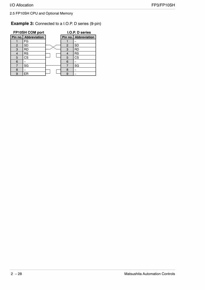
I/O Allocation FP3/FP10SH
2 − 28 Matsushita Automation Controls
2.5 FP10SH CPU and Optional Memory
Pin no. Abbreviation1 FG2 SD3 RD4 RS5 CS6 −7 SG8 −9 ER
Pin no. Abbreviation1 −2 SD3 RD4 RS5 CS6 −7 SG8 −9 −
FP10SH COM port I.O.P. D series
Example 3: Connected to a I.O.P. D series (9-pin)

I/O AllocationFP3/FP10SH
2 − 29Matsushita Automation Controls
2.5 FP10SH CPU and Optional Memory
2.5.2 Expansion Memory Unit
The expansion memory unit is installed in the FP10SH CPU.The expansion memory unit enables FP10SH to expand program memory up to60 k or 120 k steps using two following types:
Type Order number Weight
30 k steps type AFP6204 approx. 30 g/1.058 oz.
90 k steps type AFP6205
pp g/
Note
When installing and removing an expansion memory unit, thecontents of built−in RAM of CPU may be destroyed. Be sure tomake backup of program stored in the built−in RAM of CPU beforeinstalling and removing an expansion memory unit. And, if youneed, re-transfer the program to the CPU using NPST−GR software,after installation.
Installing the expansion memory unitProcedure:
1. Remove the side cover of the FP10SH CPU with aflat-head screwdriver.
Side cover Flat-headscrewdriver
next page
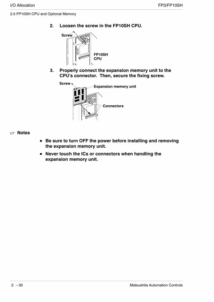
I/O Allocation FP3/FP10SH
2 − 30 Matsushita Automation Controls
2.5 FP10SH CPU and Optional Memory
2. Loosen the screw in the FP10SH CPU.
Screw
FP10SHCPU
3. Properly connect the expansion memory unit to theCPU’s connector. Then, secure the fixing screw.
ScrewExpansion memory unit
Connectors
Notes
Be sure to turn OFF the power before installing and removingthe expansion memory unit.
Never touch the ICs or connectors when handling theexpansion memory unit.

I/O AllocationFP3/FP10SH
2 − 31Matsushita Automation Controls
2.5 FP10SH CPU and Optional Memory
2.5.3 ROM Operation Board
The FP10SH can be operated using only the installed built−in RAM, but use ofcommercially available EPROM/FROM is also possible if necessary.The ROM operation board is necessary for ROM operation.
Memory (EPROM) and Master Memory (FROM)
Attach to the ROM operation board for operation.The memory (EPROM) should be used for program storage and ROM operation, andthe master memory (FROM) should be used for copying and transferring programs.CPU Ver. 2 or later is required to use the memory.
Type of FP10SH optional memories
Type Memory (EPROM) Master memory (FROM)
Using I.C. M27C2001−150F1 or equivalent SST−29EE020−150−4C−PHorequivalent
Order number AFP5209 AFP5208
Writing method Commercially available ROMprogrammer
You can write program to FROMinstalling it on the CPU.
Use Suitable for program storage orROM operation
Suitable for copyingand transmittingthe master program
Note
The I/O comments are written to the internal memory of the ROMoperation board.
Comments written to ROMThe program, system register, and initial settings (memory contents and user selectionsfor DT and other settings) are written to the memory (EPROM) or master memory(FROM). Therefore, for ROM operation, be aware that the program contents and dataregister (operation data) contents are simultaneously rewritten.The comments (line comments, comment statements, and I/O comments) are storedin the internal memory of the ROM operation board.
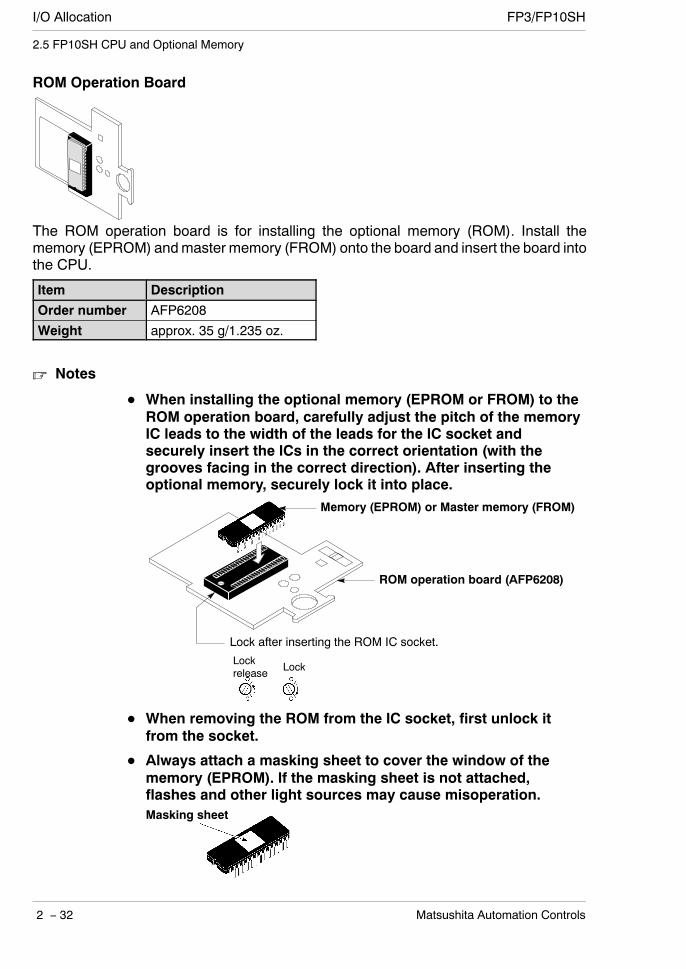
I/O Allocation FP3/FP10SH
2 − 32 Matsushita Automation Controls
2.5 FP10SH CPU and Optional Memory
ROM Operation Board
The ROM operation board is for installing the optional memory (ROM). Install thememory (EPROM) andmaster memory (FROM) onto the board and insert the board intothe CPU.
Item Description
Order number AFP6208
Weight approx. 35 g/1.235 oz.
Notes
When installing the optional memory (EPROM or FROM) to theROM operation board, carefully adjust the pitch of the memoryIC leads to the width of the leads for the IC socket andsecurely insert the ICs in the correct orientation (with thegrooves facing in the correct direction). After inserting theoptional memory, securely lock it into place.
Lock after inserting the ROM IC socket.
Lockrelease Lock
Memory (EPROM) or Master memory (FROM)
ROM operation board (AFP6208)
When removing the ROM from the IC socket, first unlock itfrom the socket.
Always attach a masking sheet to cover the window of thememory (EPROM). If the masking sheet is not attached,flashes and other light sources may cause misoperation.Masking sheet

I/O AllocationFP3/FP10SH
2 − 33Matsushita Automation Controls
2.5 FP10SH CPU and Optional Memory
Installing the ROM operation boardWhen installing the ROM operation board, first remove the FP10SH CPU from itsbackplane.
Procedure:
1. Place the CPU down flat on a surface and insert theROM operation board into the CPU along the guidesprovided. At this time, make sure that the hook on thebottom of the CPU used for attaching the unit to thebackplane is located off the table you are working on.
Insert
FP10SH CPU
ROM operationboard
2. Align the ROM operation board with its connector onthe bottom of the CPU. To make sure that the board isproperly attached, confirm it visually by lookingthrough the holes on the side of the CPU. If the boardis inserted while not aligned with the connector, thepins of the board may become bent.
Verify proper connection
next page

I/O Allocation FP3/FP10SH
2 − 34 Matsushita Automation Controls
2.5 FP10SH CPU and Optional Memory
3. Firmly press on the ROM operation board from aboveand insert it into its connector. Firmly insert theboard until its upper frame is caught on the hooks ofthe CPU (continue pushing until a catching sound isheard).
Hooks
4. To remove the board, unhook the hook by hand,insert a screwdriver into the hole provided and prythe board upwards.
Remove
Pry upwards
FP10SH CPU
ROM operationboard
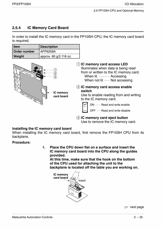
I/O AllocationFP3/FP10SH
2 − 35Matsushita Automation Controls
2.5 FP10SH CPU and Optional Memory
2.5.4 IC Memory Card Board
In order to install the IC memory card in the FP10SH CPU, the IC memory card boardis required.
Item Description
Order number AFP6209A
Weight approx. 60 g/2.116 oz.
123
IC memorycard board
1 IC memory card access LEDIlluminates when data is being readfrom or written to the IC memory card.When lit AccessingWhen not lit Not accessing
2 IC memory card access enableswitchUse to enable reading from and writingto the IC memory card.
3 IC memory card eject buttonUse to remove the IC memory card.
ON Read and write enable
OFF Read and write disable
Installing the IC memory card boardWhen installing the IC memory card board, first remove the FP10SH CPU from itsbackplane.
Procedure:1. Place the CPU down flat on a surface and insert the
IC memory card board into the CPU along the guidesprovided.At this time, make sure that the hook on the bottomof the CPU used for attaching the unit to thebackplane is located off the table you are working on.
Insert
IC memorycard board
next page

I/O Allocation FP3/FP10SH
2 − 36 Matsushita Automation Controls
2.5 FP10SH CPU and Optional Memory
2. Align the IC memory card board with its connector onthe bottom of the CPU. To make sure that the board isproperly attached, confirm it visually by lookingthrough the holes on the side of the CPU. If the boardis inserted while not aligned with the connector, thepins of the board may become bent.
Verify proper connection
3. Firmly press on the IC memory card board fromabove and insert it into its connector. Firmly insertthe board until its upper frame is caught on thehooks of the CPU (continue pushing until a catchingsound is heard).
Hooks
4. To remove the board, unhook the hook by hand, inserta screwdriver into the hole provided and pry the boardupwards.
Remove
Pry upwards
IC memorycard board
FP10SH CPU
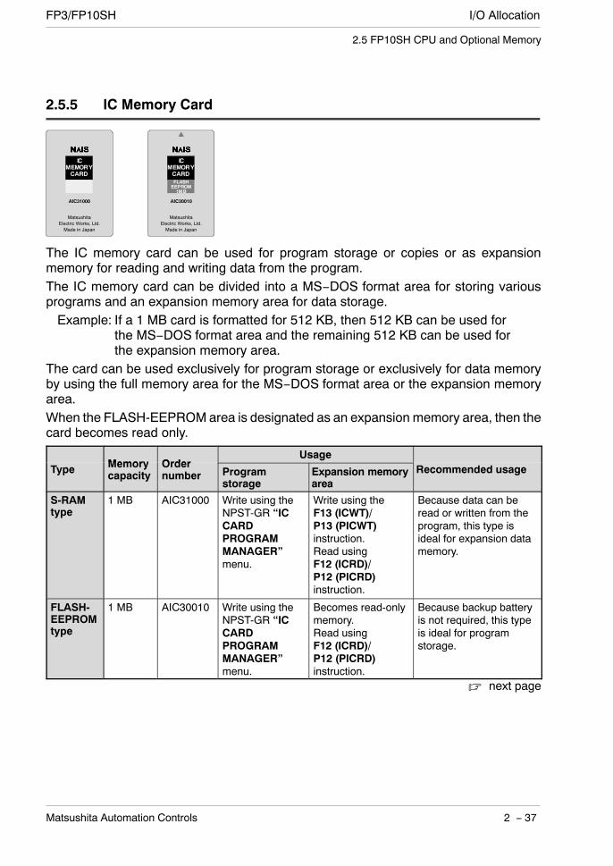
I/O AllocationFP3/FP10SH
2 − 37Matsushita Automation Controls
2.5 FP10SH CPU and Optional Memory
2.5.5 IC Memory Card
AIC30010
MatsushitaElectric Works, Ltd.Made in Japan
AIC31000
MatsushitaElectric Works, Ltd.Made in Japan
The IC memory card can be used for program storage or copies or as expansionmemory for reading and writing data from the program.The IC memory card can be divided into a MS−DOS format area for storing variousprograms and an expansion memory area for data storage.Example: If a 1 MB card is formatted for 512 KB, then 512 KB can be used for
the MS−DOS format area and the remaining 512 KB can be used forthe expansion memory area.
The card can be used exclusively for program storage or exclusively for data memoryby using the full memory area for the MS−DOS format area or the expansion memoryarea.When the FLASH-EEPROMarea is designated as an expansion memory area, then thecard becomes read only.
Memory OrderUsage
Type Memorycapacity
Ordernumber Program
storageExpansion memoryarea
Recommended usage
S-RAMtype
1 MB AIC31000 Write using theNPST-GR “ICCARDPROGRAMMANAGER”menu.
Write using theF13 (ICWT)/P13 (PICWT)instruction.Read usingF12 (ICRD)/P12 (PICRD)instruction.
Because data can beread or written from theprogram, this type isideal for expansion datamemory.
FLASH-EEPROMtype
1 MB AIC30010 Write using theNPST-GR “ICCARDPROGRAMMANAGER”menu.
Becomes read-onlymemory.Read usingF12 (ICRD)/P12 (PICRD)instruction.
Because backup batteryis not required, this typeis ideal for programstorage.
next page
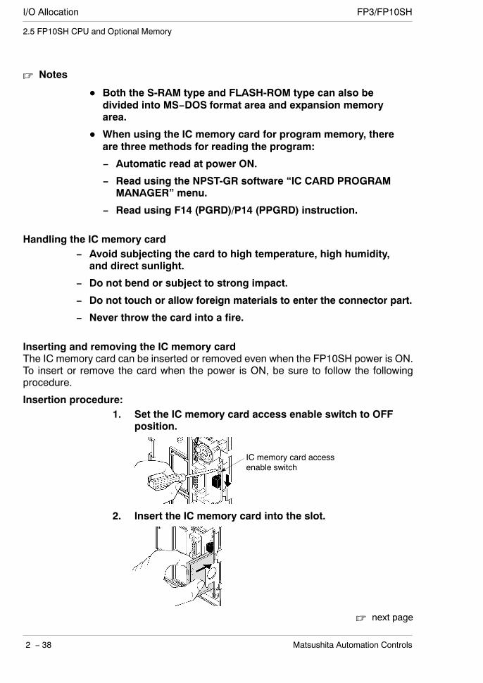
I/O Allocation FP3/FP10SH
2 − 38 Matsushita Automation Controls
2.5 FP10SH CPU and Optional Memory
Notes
Both the S-RAM type and FLASH-ROM type can also bedivided into MS−DOS format area and expansion memoryarea.
When using the IC memory card for program memory, thereare three methods for reading the program:
− Automatic read at power ON.
− Read using the NPST-GR software “IC CARD PROGRAMMANAGER” menu.
− Read using F14 (PGRD)/P14 (PPGRD) instruction.
Handling the IC memory card− Avoid subjecting the card to high temperature, high humidity,
and direct sunlight.
− Do not bend or subject to strong impact.
− Do not touch or allow foreign materials to enter the connector part.
− Never throw the card into a fire.
Inserting and removing the IC memory cardThe IC memory card can be inserted or removed even when the FP10SH power is ON.To insert or remove the card when the power is ON, be sure to follow the followingprocedure.
Insertion procedure:1. Set the IC memory card access enable switch to OFF
position.
IC memory card accessenable switch
2. Insert the IC memory card into the slot.
next page

I/O AllocationFP3/FP10SH
2 − 39Matsushita Automation Controls
2.5 FP10SH CPU and Optional Memory
3. Continue pushing the IC memory card until the ejectbutton pops out.
Eject button
4. Set the IC memory card access enable switch to ONposition.
IC memory card accessenable switch
Notes
Do not try to insert the IC memory card while the IC memorycard access enable switch is ON. It could lead to damage ofthe memory contents or a malfunction of the CPU.
Do not use excessive force on the IC memory card or slot.
Removal procedure:1. Set the IC memory card access enable switch to OFF
position. Verify that the IC memory card access LEDis OFF.
IC memory card access enable switch
IC memory card access LED
2. Push the eject button until the IC memory cardbecomes free.
Eject button
next page
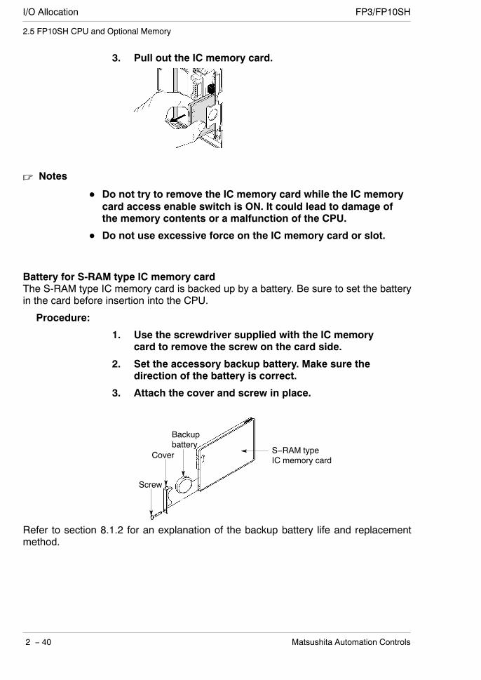
I/O Allocation FP3/FP10SH
2 − 40 Matsushita Automation Controls
2.5 FP10SH CPU and Optional Memory
3. Pull out the IC memory card.
Notes
Do not try to remove the IC memory card while the IC memorycard access enable switch is ON. It could lead to damage ofthe memory contents or a malfunction of the CPU.
Do not use excessive force on the IC memory card or slot.
Battery for S-RAM type IC memory cardThe S-RAM type IC memory card is backed up by a battery. Be sure to set the batteryin the card before insertion into the CPU.
Procedure:
1. Use the screwdriver supplied with the IC memorycard to remove the screw on the card side.
2. Set the accessory backup battery. Make sure thedirection of the battery is correct.
3. Attach the cover and screw in place.
Cover
Screw
Backupbattery
S−RAM typeIC memory card
Refer to section 8.1.2 for an explanation of the backup battery life and replacementmethod.
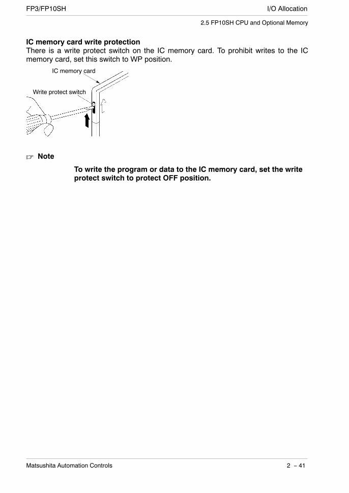
I/O AllocationFP3/FP10SH
2 − 41Matsushita Automation Controls
2.5 FP10SH CPU and Optional Memory
IC memory card write protectionThere is a write protect switch on the IC memory card. To prohibit writes to the ICmemory card, set this switch to WP position.
Write protect switch
IC memory card
Note
To write the program or data to the IC memory card, set the writeprotect switch to protect OFF position.
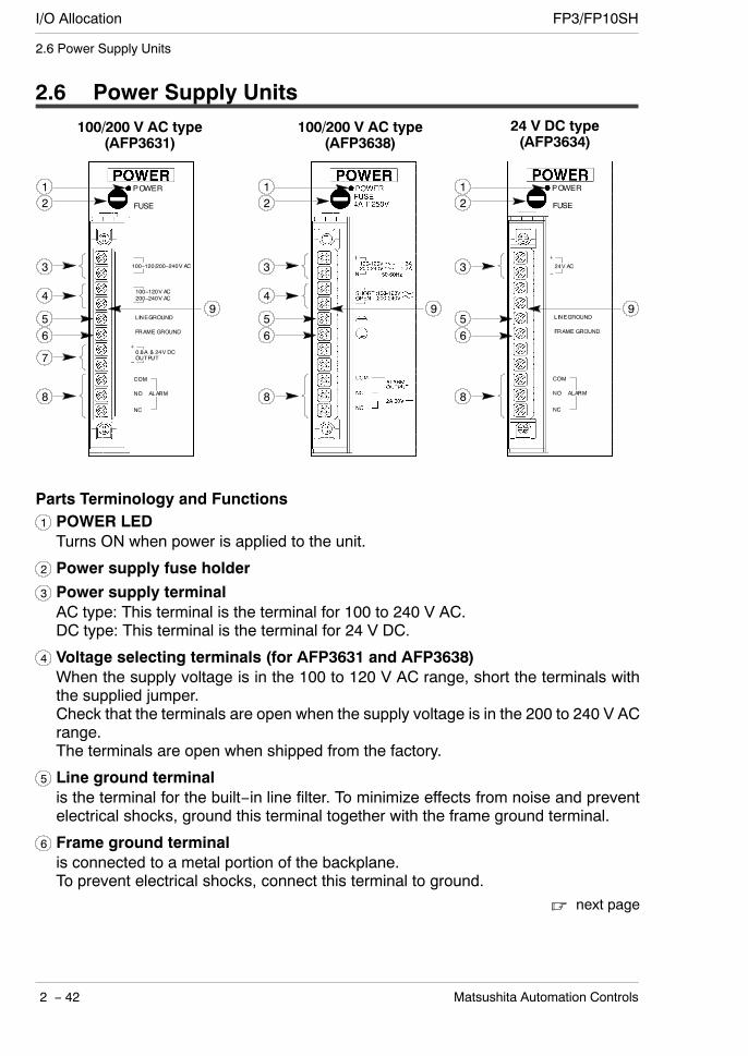
I/O Allocation FP3/FP10SH
2 − 42 Matsushita Automation Controls
2.6 Power Supply Units
2.6 Power Supply Units100/200 V AC type
(AFP3638)100/200 V AC type
(AFP3631)24 V DC type(AFP3634)
12
3
4
56
7
8
9
12
3
4
56
8
9 9
12
3
56
8
Parts Terminology and Functions1 POWER LEDTurns ON when power is applied to the unit.
2 Power supply fuse holder3 Power supply terminalAC type: This terminal is the terminal for 100 to 240 V AC.DC type: This terminal is the terminal for 24 V DC.
4 Voltage selecting terminals (for AFP3631 and AFP3638)When the supply voltage is in the 100 to 120 V AC range, short the terminals withthe supplied jumper.Check that the terminals are open when the supply voltage is in the 200 to 240 V ACrange.The terminals are open when shipped from the factory.
5 Line ground terminalis the terminal for the built−in line filter. To minimize effects from noise and preventelectrical shocks, ground this terminal together with the frame ground terminal.
6 Frame ground terminalis connected to a metal portion of the backplane.To prevent electrical shocks, connect this terminal to ground.
next page
I/O AllocationFP3/FP10SH
2 − 43Matsushita Automation Controls
2.6 Power Supply Units
7 Service power terminal (24 V DC) (for AFP3631 only)Used for the DC power supply (24 V DC) for the I/O units. The capacity will differdepending on the type of power supply unit. Do not connect this service powerterminal in parallel with the power supply for other commercially available powersupply devices.
8 Alarm output terminalContact output terminals of the relay which turns ON when the ALARM LED of theCPU turns ON. Normally closed contact (N.C.) and normally open contact (N.O.) areavailable.However, this relay operates only when the power supply unit is installed in themaster backplane.
9 Terminal blockis the terminal for power supply wiring. Uses M3.5 crimp terminals(* section 4.2.1).
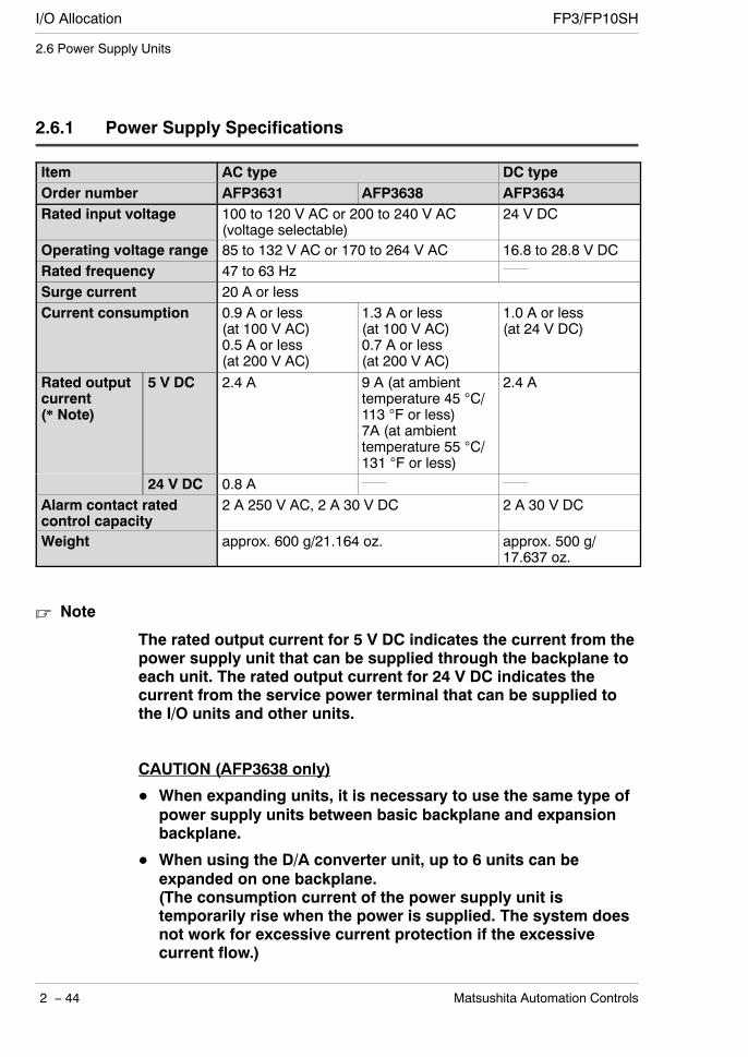
I/O Allocation FP3/FP10SH
2 − 44 Matsushita Automation Controls
2.6 Power Supply Units
2.6.1 Power Supply Specifications
Item AC type DC typeOrder number AFP3631 AFP3638 AFP3634Rated input voltage 100 to 120 V AC or 200 to 240 V AC
(voltage selectable)24 V DC
Operating voltage range 85 to 132 V AC or 170 to 264 V AC 16.8 to 28.8 V DCRated frequency 47 to 63 HzSurge current 20 A or lessCurrent consumption 0.9 A or less
(at 100 V AC)0.5 A or less(at 200 V AC)
1.3 A or less(at 100 V AC)0.7 A or less(at 200 V AC)
1.0 A or less(at 24 V DC)
Rated outputcurrent(* Note)
5 V DC 2.4 A 9 A (at ambienttemperature 45 °C/113 °F or less)7A (at ambienttemperature 55 °C/131 °F or less)
2.4 A
24 V DC 0.8 AAlarm contact ratedcontrol capacity
2 A 250 V AC, 2 A 30 V DC 2 A 30 V DC
Weight approx. 600 g/21.164 oz. approx. 500 g/17.637 oz.
Note
The rated output current for 5 V DC indicates the current from thepower supply unit that can be supplied through the backplane toeach unit. The rated output current for 24 V DC indicates thecurrent from the service power terminal that can be supplied tothe I/O units and other units.
CAUTION (AFP3638 only)
When expanding units, it is necessary to use the same type ofpower supply units between basic backplane and expansionbackplane.
When using the D/A converter unit, up to 6 units can beexpanded on one backplane.(The consumption current of the power supply unit istemporarily rise when the power is supplied. The system doesnot work for excessive current protection if the excessivecurrent flow.)
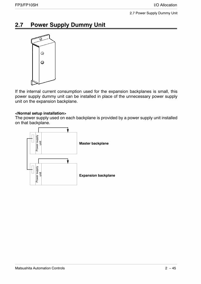
I/O AllocationFP3/FP10SH
2 − 45Matsushita Automation Controls
2.7 Power Supply Dummy Unit
2.7 Power Supply Dummy Unit
If the internal current consumption used for the expansion backplanes is small, thispower supply dummy unit can be installed in place of the unnecessary power supplyunit on the expansion backplane.
<Normal setup installation>The power supply used on each backplane is provided by a power supply unit installedon that backplane.
Pow
ersupply
unit
Pow
ersupply
unit
Master backplane
Expansion backplane
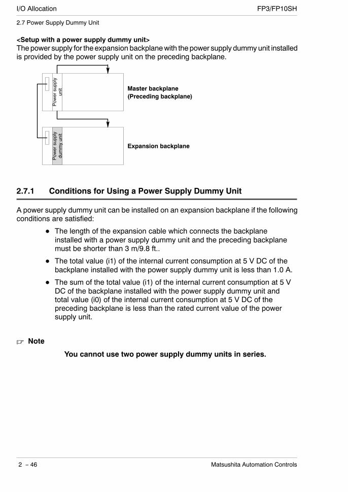
I/O Allocation FP3/FP10SH
2 − 46 Matsushita Automation Controls
2.7 Power Supply Dummy Unit
<Setup with a power supply dummy unit>Thepower supply for theexpansion backplanewith the power supply dummyunit installedis provided by the power supply unit on the preceding backplane.
Pow
ersupply
unit
Pow
ersupply
dummyunit
Master backplane(Preceding backplane)
Expansion backplane
2.7.1 Conditions for Using a Power Supply Dummy Unit
A power supply dummy unit can be installed on an expansion backplane if the followingconditions are satisfied:
The length of the expansion cable which connects the backplaneinstalled with a power supply dummy unit and the preceding backplanemust be shorter than 3 m/9.8 ft..
The total value (i1) of the internal current consumption at 5 V DC of thebackplane installed with the power supply dummy unit is less than 1.0 A.
The sum of the total value (i1) of the internal current consumption at 5 VDC of the backplane installed with the power supply dummy unit andtotal value (i0) of the internal current consumption at 5 V DC of thepreceding backplane is less than the rated current value of the powersupply unit.
Note
You cannot use two power supply dummy units in series.

I/O AllocationFP3/FP10SH
2 − 47Matsushita Automation Controls
2.7 Power Supply Dummy Unit
Example 1:When the power supply dummy unit is installed on the 1st expansion backplane
Conditionsi0 + i1≦Rated current value of powersupply unit (1)i1≦ 1 AL1≦ 3 m/9.8 ft.
i0: Total value of internal currentconsumption at 5 V DC of the masterbackplane with the power supplyunit (1).
i1: Total value of internal currentconsumption at 5 V DC of the 1stexpansion backplane with the powersupply dummy unit.
L1: Length of expansion cable betweenthe master backplane and the 1stexpansion backplane.
Master backplanePow
ersupply
unit(1)
CPU
Pow
ersupply
unit(2)
i0
i1
L1
1st expansion backplane
2nd expansion backplane
Pow
ersupply
dummyunit
Example 2:When the power supply dummy unit is installed on the 2nd expansion backplane
Conditions∆ i0 + i1≦Rated current value of power
supply unit (2)∆ i1≦ 1 A∆ L2≦ 3 m/9.8 ft.
i0: Total value of internal currentconsumption at 5 V DC of the 1stexpansion backplane with thepower supply unit (2).
i1: Total value of internal currentconsumption at 5 V DC of the 2ndexpansion backplane with thepower supply dummy unit.
L2: Length of the expansion cablebetween the 1st expansionbackplane and the 2nd expansionbackplane .
Master backplane
Pow
ersupply
unit(1)
CPU
Pow
ersupply
unit(2) i0
i1
L1
L2
1st expansion backplane
2nd expansion backplane
Pow
ersupply
dummyunit
NoteRefor to section 1.3.3, for detalis about the current consumptionof each unit.
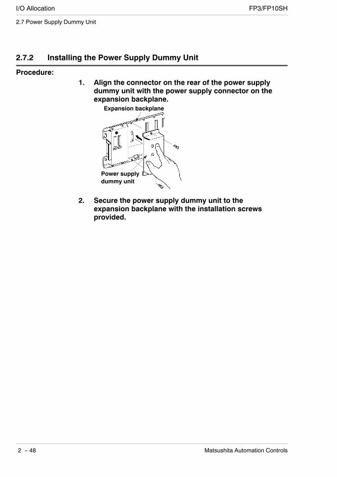
I/O Allocation FP3/FP10SH
2 − 48 Matsushita Automation Controls
2.7 Power Supply Dummy Unit
2.7.2 Installing the Power Supply Dummy Unit
Procedure:1. Align the connector on the rear of the power supply
dummy unit with the power supply connector on theexpansion backplane.
Expansion backplane
Power supplydummy unit
2. Secure the power supply dummy unit to theexpansion backplane with the installation screwsprovided.
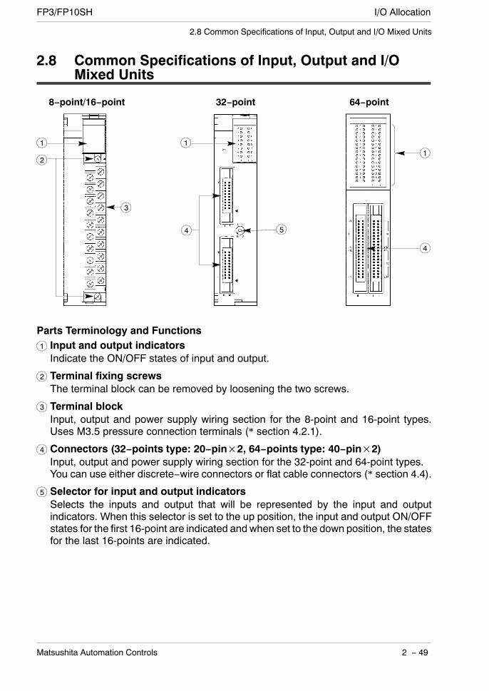
I/O AllocationFP3/FP10SH
2 − 49Matsushita Automation Controls
2.8 Common Specifications of Input, Output and I/O Mixed Units
2.8 Common Specifications of Input, Output and I/OMixed Units
8−point/16−point 32−point 64−point
1
2
3
4 5
1
4
1
Parts Terminology and Functions1 Input and output indicatorsIndicate the ON/OFF states of input and output.
2 Terminal fixing screwsThe terminal block can be removed by loosening the two screws.
3 Terminal blockInput, output and power supply wiring section for the 8-point and 16-point types.Uses M3.5 pressure connection terminals (* section 4.2.1).
4 Connectors (32−points type: 20−pin×2, 64−points type: 40−pin×2)Input, output and power supply wiring section for the 32-point and 64-point types.You can use either discrete−wire connectors or flat cable connectors (* section 4.4).
5 Selector for input and output indicatorsSelects the inputs and output that will be represented by the input and outputindicators. When this selector is set to the up position, the input and output ON/OFFstates for the first 16-point are indicated and when set to the down position, the statesfor the last 16-points are indicated.
I/O Allocation FP3/FP10SH
2 − 50 Matsushita Automation Controls
2.8 Common Specifications of Input, Output and I/O Mixed Units
2.8.1 Table of Input Unit Types
Type Numberof points
Connectionmethod
Description Order number
DC inputtype
16-point terminal 12 to 24 V DC, sink/sourceinput
AFP33023−Ftype
32-point connector 12 to 24 V DC, sink/sourceinput
AFP33024−F
5 V DC, sink/source input AFP33014−F64-point connector 12 to 24 V DC, sink/source
inputAFP33027−F
5 V DC, sink/source input AFP33017−Fhigh-speed response type, 12to 24 V DC, sink/source input
AFP33028−F
high-speed response type,24 V DC, sink/source input
AFP33068−F
AC input 8-point terminal 100 to 120 V AC AFP33041ptype
p200 to 240 V AC AFP33051
16-point terminal 100 to 120 V AC AFP33043p200 to 240 V AC AFP33053
2.8.2 Table of Output Unit Types
Type Numberof points
Connectionmethod
Description Order number
Relay 16-point terminal without relay sockets, 2 A/point AFP33103−Fyoutput type
pwith relay sockets, 2 A/point AFP33203−F
Transistor(NPN open
16-point terminal 5 to 24 V DC, 0.5 A AFP33483−F(NPN opencollector)
32-point connector 5 to 24 V DC, 0.1 A AFP33484−Fcollector)output type 64-point 5 to 24 V DC, 0.1 A AFP33487−F
Transistor(PNP open
16-point terminal 5 to 24 V DC, 0.1 A AFP33583−F(PNP opencollector)
32-point connector 5 to 24 V DC, 0.1 A AFP33584−Fcollector)output type 64-point 5 to 24 V DC, 0.1 A AFP33587−F
Triac outputtype
16-point terminal 100 to 240 V AC, 0.5 A/point AFP33703
Note
The maximum load current for the transistor output type outputunit will differ depending on the voltage used.Refer to the specifications pages for each unit.
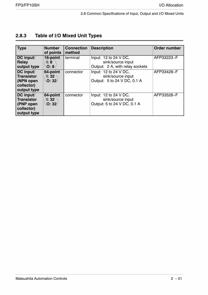
I/O AllocationFP3/FP10SH
2 − 51Matsushita Automation Controls
2.8 Common Specifications of Input, Output and I/O Mixed Units
2.8.3 Table of I/O Mixed Unit Types
Type Numberof points
Connectionmethod
Description Order number
DC input/Relayoutput type
16-pointI: 8O: 8
terminal Input: 12 to 24 V DC,sink/source input
Output: 2 A, with relay sockets
AFP33223−F
DC input/Transistor(NPN opencollector)output type
64-pointI: 32O: 32
connector Input: 12 to 24 V DC,sink/source input
Output: 5 to 24 V DC, 0.1 A
AFP33428−F
DC input/Transistor(PNP opencollector)output type
64-pointI: 32O: 32
connector Input: 12 to 24 V DC,sink/source input
Output: 5 to 24 V DC, 0.1 A
AFP33528−F

I/O Allocation FP3/FP10SH
2 − 52 Matsushita Automation Controls
2.9 Input Units Specifications
2.9 Input Units Specifications
2.9.1 16-point Type DC Input Unit
2.9.1.1 Specifications
Item DescriptionOrder number AFP33023−FRated input voltage 12 to 24 V DCRated input current approx. 8 mA (at 24 V DC)Input impedance approx. 3 k ΩInput voltage range 10.2 to 26.4 V DC
(max. input current: 10 mA or less)Min. ON voltage/Min. ON current
9.6 V/4 mA
Max. OFF voltage/Max. OFF current
2.5 V/1 mA
Responsei
OFF→ ON 1.5 ms or lessptime ON→ OFF 2.0 ms or lessInternal currentconsumption (at 5 V DC)
60 mA or less
Input points per common 8 points/commonEither the positive or negative of the input power supply canbe connected to COM (common) terminal.
Connection method terminal block (M 3.5 screw)Weight approx. 300 g/10.582 oz

I/O AllocationFP3/FP10SH
2 − 53Matsushita Automation Controls
2.9 Input Units Specifications
2.9.1.2 Internal Circuit Diagram
COM
Input
Internalcircuit
InputindicatorLED
1.5 kΩ
1.5 kΩ
1 kΩ0.1 µF12 to24 V DC
AFP33023−F
2.9.1.3 Pin Layout of Terminal Block
12 to24 V DC
12 to24 V DC
0
2
4
6
1
3
5
7COM(+, −)
9
B
D
8
A
C
E
COM(+, −)
F
Σ
Σ
AFP33023−F
Note
For more information regarding the applicable pressureconnection (crimp) terminals and wiring, refer to section 4.5.

I/O Allocation FP3/FP10SH
2 − 54 Matsushita Automation Controls
2.9 Input Units Specifications
2.9.2 32-point Type DC Input Units
2.9.2.1 Specifications
Item DescriptionOrder number AFP33024−F AFP33014−FRated input voltage 12 to 24 V DC 5 V DCRated input current approx. 8 mA (at 24 V DC) approx. 4.2 mA (at 5 V DC)Input impedance approx. 3 k Ω approx. 1.2 k ΩInput voltage range 10.2 to 26.4 V DC 4.25 to 5.5 V DCMin. ON voltage/Min. ON current
9.6 V/4 mA 3.5 V/3 mA
Max. OFF voltage/Max. OFF current
2.5 V/1 mA 1.5 V/1 mA
Responsei
OFF→ ON 1.5 ms or lessptime ON→ OFF 2.0 ms or lessInternal currentconsumption (at 5 V DC)
120 mA or less
Input points per common 16 points/commonEither the positive or negative of the input power supply canbe connected to COM (common) terminal.
Connection method two 20-pin connectorsWeight approx. 400 g/14.110 oz
When an AFP33024−F is used, keep the rate of input points per common which aresimultaneously ON within the following range as determined by the ambienttemperature.
Rate of input pointsper common whichare simultaneousON (%)
Ambient temperature (°C/°F)
at 24 V DC
at 26.4 V DC
55/131
50/122
35/95
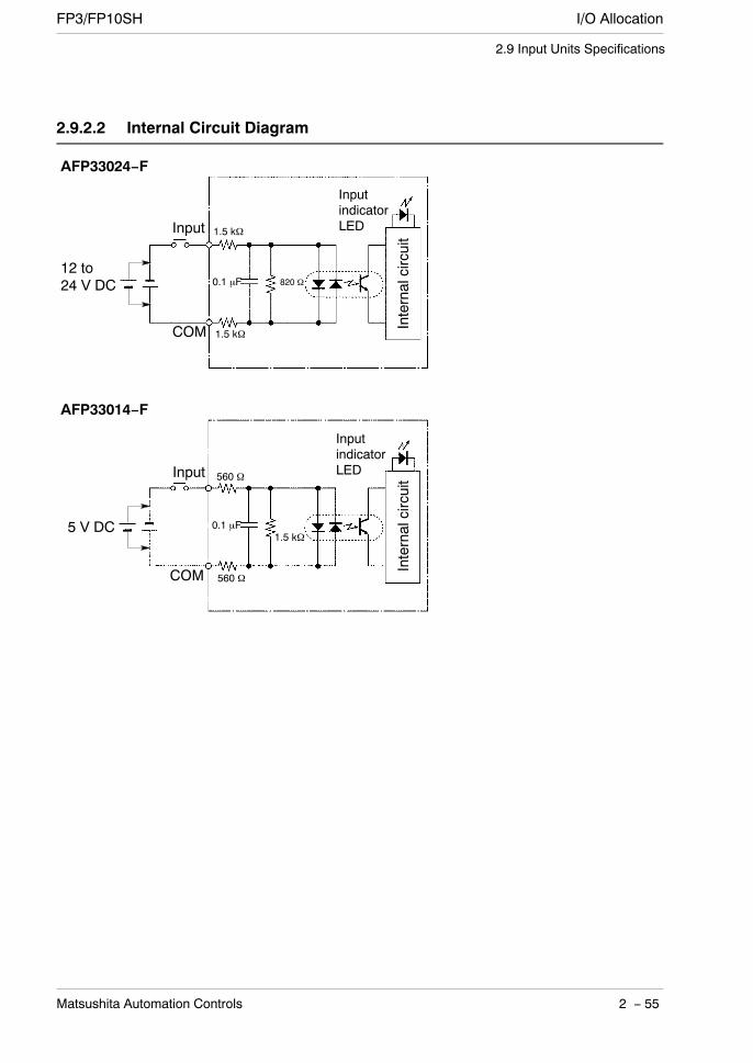
I/O AllocationFP3/FP10SH
2 − 55Matsushita Automation Controls
2.9 Input Units Specifications
2.9.2.2 Internal Circuit Diagram
820 Ω
COM
Input 1.5 kΩ
1.5 kΩ
0.1 µF12 to24 V DC
AFP33024−F
InputindicatorLED
Internalcircuit
COM
Input
Internalcircuit560 Ω
560 Ω
1.5 kΩ0.1 µF
AFP33014−F
InputindicatorLED
5 V DC
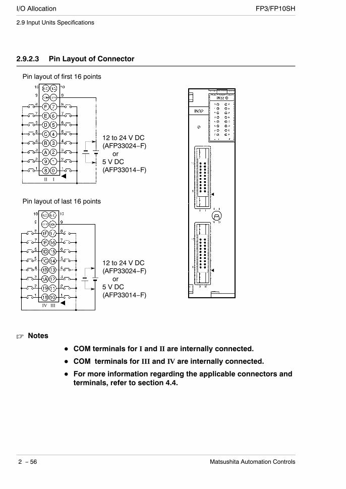
I/O Allocation FP3/FP10SH
2 − 56 Matsushita Automation Controls
2.9 Input Units Specifications
2.9.2.3 Pin Layout of Connector
12 to 24 V DC(AFP33024−F)
or5 V DC(AFP33014−F)
12 to 24 V DC(AFP33024−F)
or5 V DC(AFP33014−F)
II I
IV III
Pin layout of first 16 points
Pin layout of last 16 points
Notes
COM terminals for I and II are internally connected.
COM terminals for III and IV are internally connected.
For more information regarding the applicable connectors andterminals, refer to section 4.4.

I/O AllocationFP3/FP10SH
2 − 57Matsushita Automation Controls
2.9 Input Units Specifications
2.9.3 64-point Type DC Input Units
2.9.3.1 Specifications
Item DescriptionOrder number AFP33027−F AFP33017−FRated input voltage 12 to 24 V DC 5 V DCRated input current approx. 6.2 mA (at 24 V DC) approx. 4.2 mA (at 5 V DC)Input impedance approx. 3.9 k Ω approx. 1.2 k ΩInput voltage range 10.2 to 26.4 V DC 4.25 to 5.5 V DCMin. ON voltage/Min. ON current
9.6 V/3 mA 3.5 V/3 mA
Max. OFF voltage/Max. OFF current
2.5 V/1 mA 1.5 V/1 mA
Responsei
OFF→ ON 1.5 ms or lessptime ON→ OFF 2.0 ms or lessInternal currentconsumption (at 5 V DC)
230 mA or less
Input points per common 32 points/commonEither the positive or negative of the input power supply canbe connected to COM (common) terminal.
Connection method two 40-pin connectorsWeight approx. 400 g/14.110 oz
2.9.3.2 Internal Circuit Diagram
12 to24 V DC(AFP33027−F)
or5 V DC(AFP33017−F)
AFP33017−F/AFP33027−F
COM
InputInternal current consumptionswitch (SW1 and SW2)(* section 2.9.3.4)
Internalcircuit
InputindicatorLED
3.9 kΩ (AFP33027−F)1.2 kΩ (AFP33017−F)
1 kΩ (AFP33027−F)1.5 kΩ (AFP33017−F)
Switchingcircuit
ON
OFF

I/O Allocation FP3/FP10SH
2 − 58 Matsushita Automation Controls
2.9 Input Units Specifications
2.9.3.3 Pin Layout of Connector
III
IV
I
II
12 to24 V DC(AFP33027−F)
or5 V DC(AFP33017−F)
Pin layout of first 32 pointsleft side connector
Pin layout of last 32 pointsright side connector
12 to24 V DC(AFP33027−F)
or5 V DC(AFP33017−F)
. next page
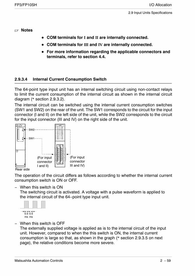
I/O AllocationFP3/FP10SH
2 − 59Matsushita Automation Controls
2.9 Input Units Specifications
Notes
COM terminals for I and II are internally connected.
COM terminals for III and IV are internally connected.
For more information regarding the applicable connectors andterminals, refer to section 4.4.
2.9.3.4 Internal Current Consumption Switch
The 64-point type input unit has an internal switching circuit using non-contact relaysto limit the current consumption of the internal circuit as shown in the internal circuitdiagram (* section 2.9.3.2).The internal circuit can be switched using the internal current consumption switches(SW1 and SW2) on the rear of the unit. The SW1 corresponds to the circuit for the inputconnector (I and II) on the left side of the unit, while the SW2 corresponds to the circuitfor the input connector (III and IV) on the right side of the unit.
SW2
SW1
(For inputconnectorI and II)
(For inputconnectorIII and IV)
Rear side
The operation of the circuit differs as follows according to whether the internal currentconsumption switch is ON or OFF.
− When this switch is ONThe switching circuit is activated. A voltage with a pulse waveform is applied tothe internal circuit of the 64−point type input unit.
0.5ms
0.5ms
− When this switch is OFFThe externally supplied voltage is applied as is to the internal circuit of the inputunit. However, compared to when the this switch is ON, the internal currentconsumption is large so that, as shown in the graph (* section 2.9.3.5 on nextpage), the relative conditions become more severe.

I/O Allocation FP3/FP10SH
2 − 60 Matsushita Automation Controls
2.9 Input Units Specifications
2.9.3.5 Limitations on Number of Simultaneous Input ON Points
Keep the number of input points per common which are simultaneously ON within thefollowing range as determined by the temperature.When internal current consumptionswitch SW1 and SW2 are both OFF(settings at time of shipment from thefactory)
When either internal current consumptionswitch SW1 or SW2 is ON
100
8070
29/84.2 48/118.4 55/131
at 24 VDCat 26.4 VDC
1009080
55/131
52/125.6
46/114.8
at 24 VDCat 26.4 VDC
Ambient temperature (_C/_F)Ambient temperature (_C/_F)
Rate of inputpoints percommonwhich aresimultaneousON (%)
Rate of inputpoints percommonwhich aresimultaneousON (%)
There is no limit when the internal current consumption switch SW1 and SW2 are bothON.There is no limit when using 12 V DC.
2.9.3.6 Notes Regarding the Internal Current Consumption Switch Settings
When using two-wire type sensor or proximity sensors, be sure to turn OFF the internalcurrent consumption switch corresponding to the circuit connected to the sensor.When adding an operation verification LED in parallel with the input contact, ordepending on the type of sensor used, there is a danger that the current will leak intoanother input circuit and cause erroneous operation. When this happens, either turnOFF the internal current consumption switch to the problem circuit or insert a diode intothe input circuit (* section 4.3.1.6).
COM
Input
Insert diode
Inputcontact
OperationLED
Internalcircuit
64−point typeDC input unit
Note
The dotted line represents reversal of input voltage polarity.
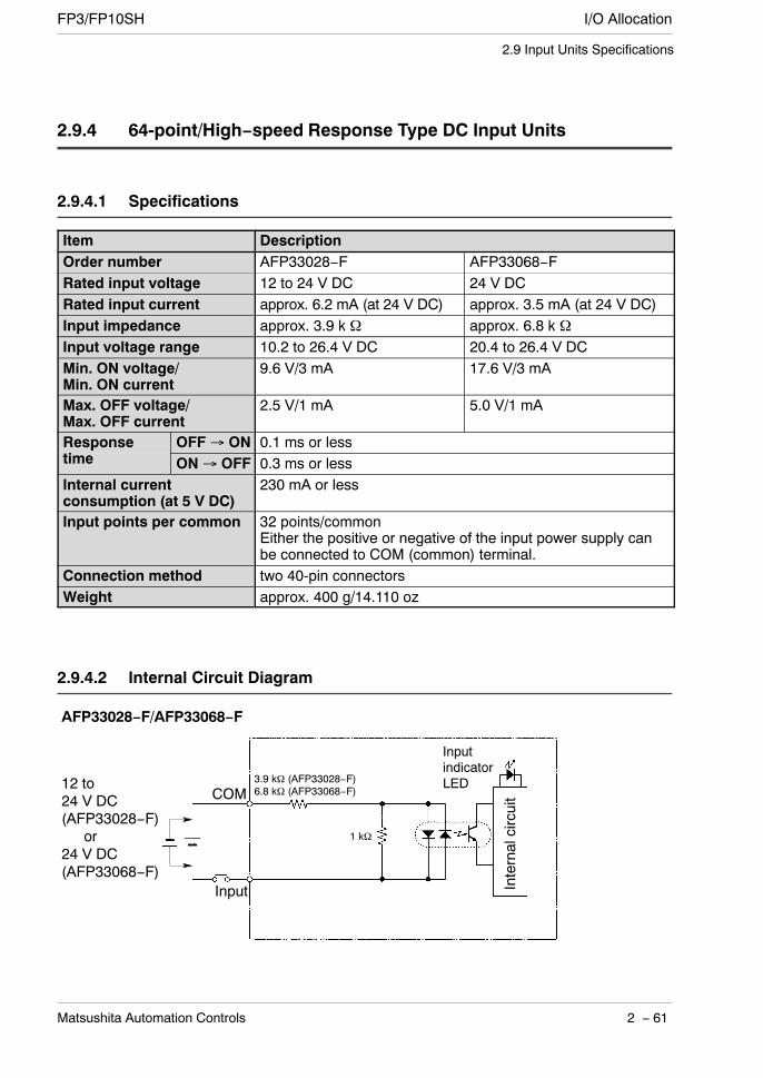
I/O AllocationFP3/FP10SH
2 − 61Matsushita Automation Controls
2.9 Input Units Specifications
2.9.4 64-point/High−speed Response Type DC Input Units
2.9.4.1 Specifications
Item DescriptionOrder number AFP33028−F AFP33068−FRated input voltage 12 to 24 V DC 24 V DCRated input current approx. 6.2 mA (at 24 V DC) approx. 3.5 mA (at 24 V DC)Input impedance approx. 3.9 k Ω approx. 6.8 k ΩInput voltage range 10.2 to 26.4 V DC 20.4 to 26.4 V DCMin. ON voltage/Min. ON current
9.6 V/3 mA 17.6 V/3 mA
Max. OFF voltage/Max. OFF current
2.5 V/1 mA 5.0 V/1 mA
Responsei
OFF→ ON 0.1 ms or lessptime ON→ OFF 0.3 ms or lessInternal currentconsumption (at 5 V DC)
230 mA or less
Input points per common 32 points/commonEither the positive or negative of the input power supply canbe connected to COM (common) terminal.
Connection method two 40-pin connectorsWeight approx. 400 g/14.110 oz
2.9.4.2 Internal Circuit Diagram
12 to24 V DC(AFP33028−F)
or24 V DC(AFP33068−F)
AFP33028−F/AFP33068−F
COM
Input Internalcircuit
InputindicatorLED3.9 kΩ (AFP33028−F)
6.8 kΩ (AFP33068−F)
1 kΩ

I/O Allocation FP3/FP10SH
2 − 62 Matsushita Automation Controls
2.9 Input Units Specifications
2.9.4.3 Pin Layout of Connector
III
IV
I
II
12 to24 V DC(AFP33028−F)
or24 V DC(AFP33068−F)
Pin layout of first 32 pointsleft side connector
Pin layout of last 32 pointsright side connector
12 to24 V DC(AFP33028−F)
or24 V DC(AFP33068−F)
next page
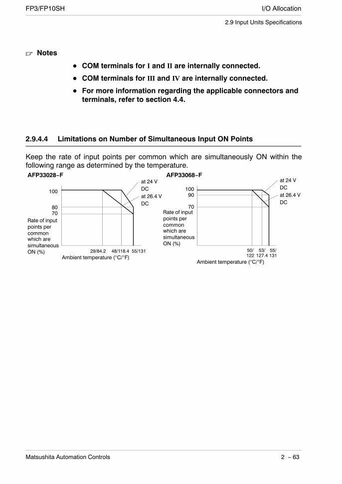
I/O AllocationFP3/FP10SH
2 − 63Matsushita Automation Controls
2.9 Input Units Specifications
Notes
COM terminals for I and II are internally connected.
COM terminals for III and IV are internally connected.
For more information regarding the applicable connectors andterminals, refer to section 4.4.
2.9.4.4 Limitations on Number of Simultaneous Input ON Points
Keep the rate of input points per common which are simultaneously ON within thefollowing range as determined by the temperature.AFP33028−F
100
8070
29/84.2 48/118.4 55/131
at 24 VDCat 26.4 VDC
10090
70
55/131
53/127.4
50/122
at 24 VDCat 26.4 VDC
Ambient temperature (°C/°F)Ambient temperature (°C/°F)
AFP33068−F
Rate of inputpoints percommonwhich aresimultaneousON (%)
Rate of inputpoints percommonwhich aresimultaneousON (%)

I/O Allocation FP3/FP10SH
2 − 64 Matsushita Automation Controls
2.9 Input Units Specifications
2.9.5 8-point Type AC Input Units
2.9.5.1 Specifications
Item DescriptionOrder number AFP33041 AFP33051Rated input voltage 100 to 120 V AC 200 to 240 V ACRated input current approx. 10 mA (at 100 V AC) approx. 10 mA (at 200 V AC)Input impedance approx. 10 k Ω approx. 20 k ΩInput voltage range 85 to 132 V AC (max. input
current: 20 mA or less)170 to 264 V AC (max. inputcurrent: 20 mA or less)
Min. ON voltage/Min. ON current
80 V/6 mA 160 V/6 mA
Max. OFF voltage/Max. OFF current
30 V/3 mA 50 V/3 mA
Responsei
OFF→ ON 15 ms or lessptime ON→ OFF 30 ms or lessInternal currentconsumption (at 5 V DC)
60 mA or less
Input points per common 8 points/commonConnection method terminal block (M 3.5 screw)Weight approx. 350 g/12.346 oz
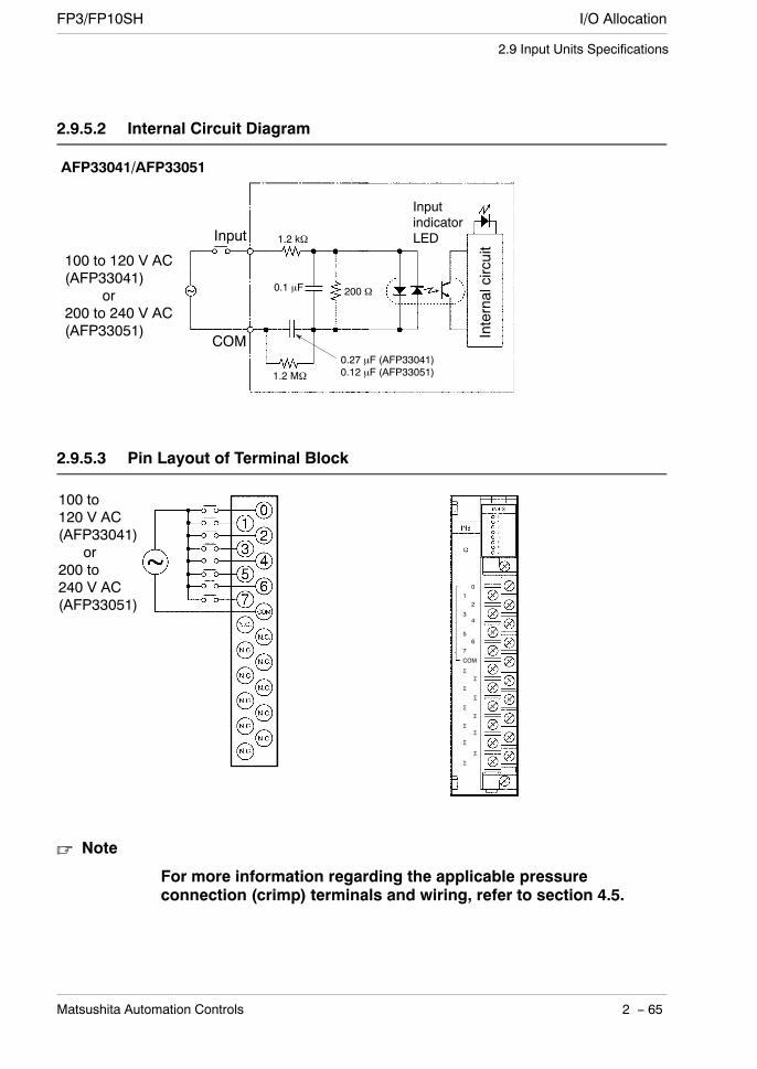
I/O AllocationFP3/FP10SH
2 − 65Matsushita Automation Controls
2.9 Input Units Specifications
2.9.5.2 Internal Circuit Diagram
COM
Input
Internalcircuit
InputindicatorLED1.2 kΩ
1.2 MΩ
200 Ω0.1 µF
100 to 120 V AC(AFP33041)
or200 to 240 V AC(AFP33051)
AFP33041/AFP33051
0.27 µF (AFP33041)0.12 µF (AFP33051)
2.9.5.3 Pin Layout of Terminal Block
100 to120 V AC(AFP33041)
or200 to240 V AC(AFP33051)
0
2
4
6
1
3
5
7
COM
Σ
Σ
Σ
Σ
Σ
Σ
Σ
Σ
Σ
Σ
Σ
Note
For more information regarding the applicable pressureconnection (crimp) terminals and wiring, refer to section 4.5.

I/O Allocation FP3/FP10SH
2 − 66 Matsushita Automation Controls
2.9 Input Units Specifications
2.9.6 16-point Type AC Input Units
2.9.6.1 Specifications
Item DescriptionOrder number AFP33043 AFP33053Rated input voltage 100 to 120 V AC 200 to 240 V ACRated input current approx. 10 mA (at 100 V AC) approx. 10 mA (at 200 V AC)Input impedance approx. 10 k Ω approx. 20 k ΩInput voltage range 85 to 132 V AC
(max. input current: 20 mA orless)
170 to 264 V AC(max. input current: 20 mA orless)
Min. ON voltage/Min. ON current
80 V/6 mA 160 V/6 mA
Max. OFF voltage/Max. OFF current
30 V/3 mA 50 V/3 mA
Responsei
OFF→ ON 15 ms or lessptime ON→ OFF 30 ms or lessInternal currentconsumption (at 5 V DC)
60 mA or less
Input points per common 8 points/commonConnection method terminal block (M 3.5 screw)Weight approx. 350 g/12.346 oz
Limitations on Number of Simultaneous Input ON Points
Keep the number of input points per common which are simultaneously ON within thefollowing range as determined by the ambient temperature.
Number ofinput pointsper commonwhich aresimultaneousON
Ambient temperature (°C/°F) Ambient temperature (°C/°F)
AFP33043 AFP33053
Number ofinput pointsper commonwhich aresimultaneousON
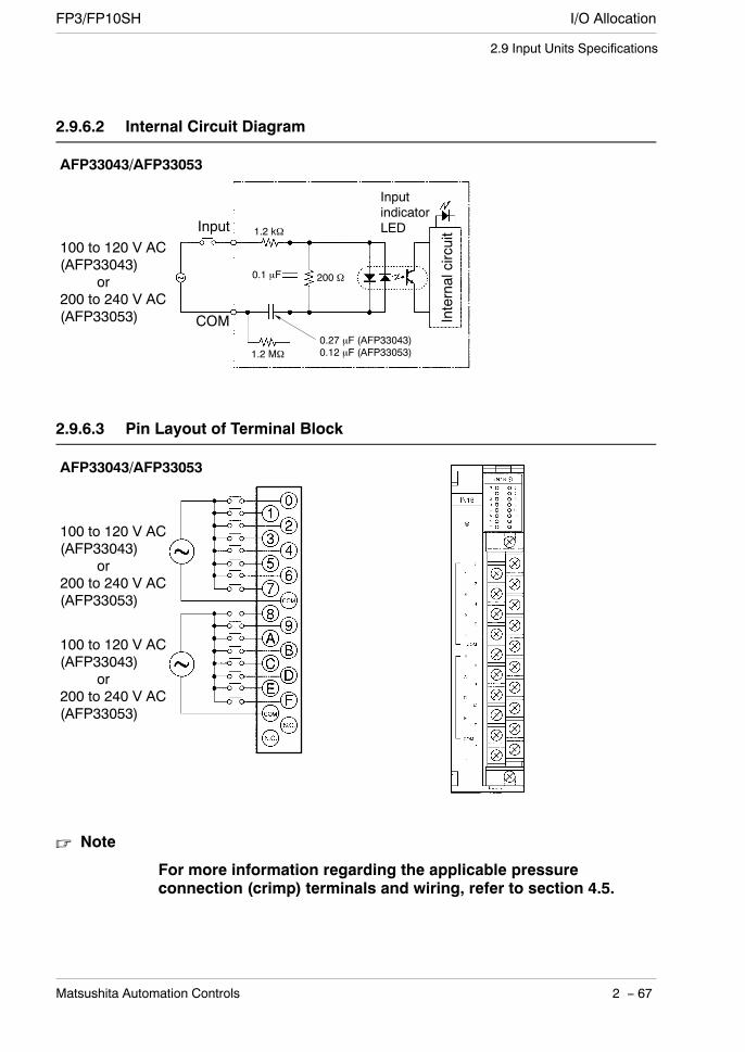
I/O AllocationFP3/FP10SH
2 − 67Matsushita Automation Controls
2.9 Input Units Specifications
2.9.6.2 Internal Circuit Diagram
Internalcircuit
InputindicatorLED
100 to 120 V AC(AFP33043)
or200 to 240 V AC(AFP33053)
0.27 µF (AFP33043)0.12 µF (AFP33053)
COM
Input 1.2 kΩ
1.2 MΩ
200 Ω0.1 µF
AFP33043/AFP33053
2.9.6.3 Pin Layout of Terminal Block
AFP33043/AFP33053
100 to 120 V AC(AFP33043)
or200 to 240 V AC(AFP33053)
100 to 120 V AC(AFP33043)
or200 to 240 V AC(AFP33053)
Note
For more information regarding the applicable pressureconnection (crimp) terminals and wiring, refer to section 4.5.
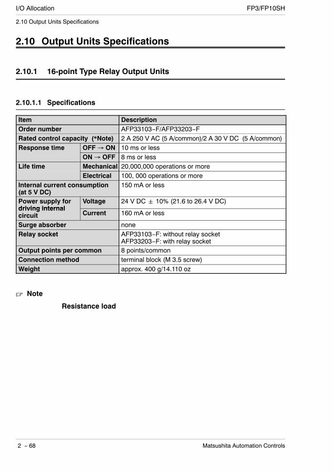
I/O Allocation FP3/FP10SH
2 − 68 Matsushita Automation Controls
2.10 Output Units Specifications
2.10 Output Units Specifications
2.10.1 16-point Type Relay Output Units
2.10.1.1 Specifications
Item DescriptionOrder number AFP33103−F/AFP33203−FRated control capacity (*Note) 2 A 250 V AC (5 A/common)/2 A 30 V DC (5 A/common)Response time OFF→ ON 10 ms or lessp
ON→ OFF 8 ms or lessLife time Mechanical 20,000,000 operations or more
Electrical 100, 000 operations or moreInternal current consumption(at 5 V DC)
150 mA or less
Power supply fordriving internal
Voltage 24 V DC 10% (21.6 to 26.4 V DC)driving internalcircuit Current 160 mA or less
Surge absorber noneRelay socket AFP33103−F: without relay socket
AFP33203−F: with relay socketOutput points per common 8 points/commonConnection method terminal block (M 3.5 screw)Weight approx. 400 g/14.110 oz
Note
Resistance load
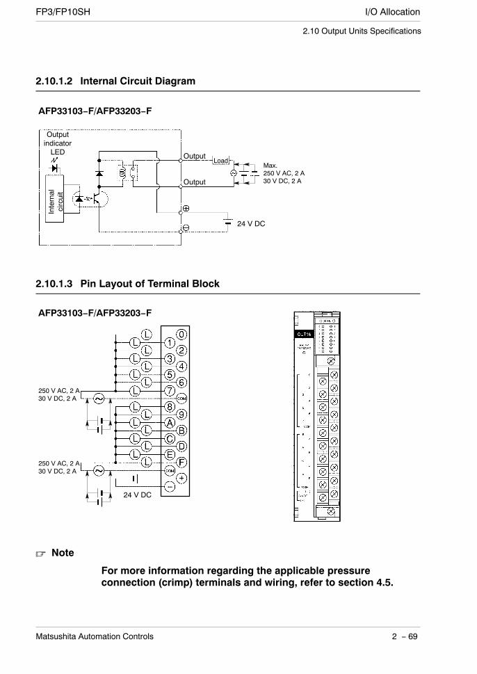
I/O AllocationFP3/FP10SH
2 − 69Matsushita Automation Controls
2.10 Output Units Specifications
2.10.1.2 Internal Circuit Diagram
Max.250 V AC, 2 A30 V DC, 2 A
Output
Internal
circuit
OutputindicatorLED
Load
Output
24 V DC
AFP33103−F/AFP33203−F
2.10.1.3 Pin Layout of Terminal Block
250 V AC, 2 A30 V DC, 2 A
250 V AC, 2 A30 V DC, 2 A
24 V DC
AFP33103−F/AFP33203−F
Note
For more information regarding the applicable pressureconnection (crimp) terminals and wiring, refer to section 4.5.
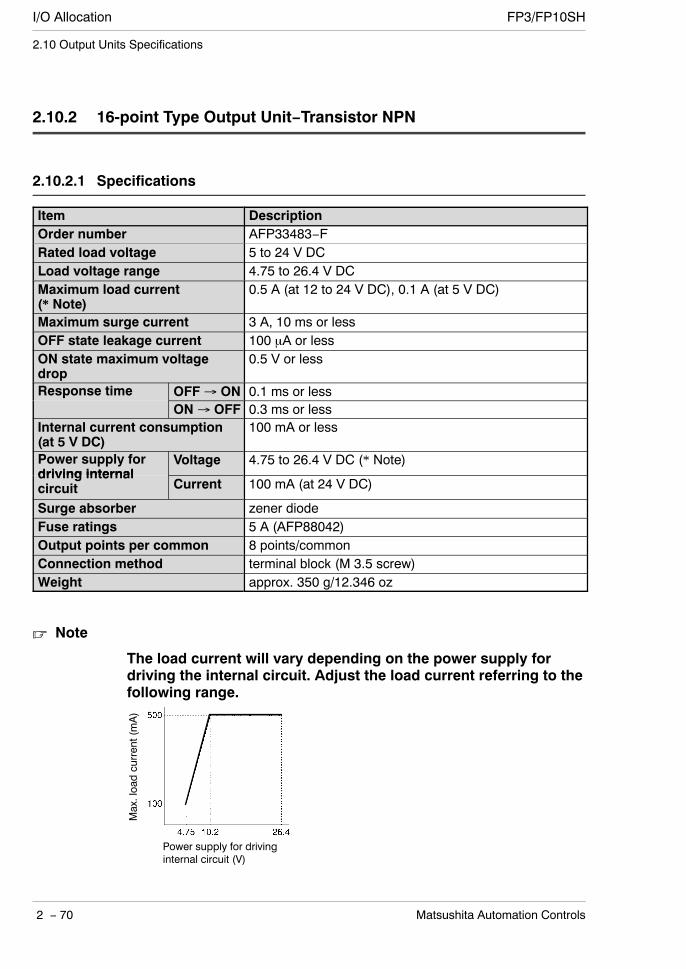
I/O Allocation FP3/FP10SH
2 − 70 Matsushita Automation Controls
2.10 Output Units Specifications
2.10.2 16-point Type Output Unit−Transistor NPN
2.10.2.1 Specifications
Item DescriptionOrder number AFP33483−FRated load voltage 5 to 24 V DCLoad voltage range 4.75 to 26.4 V DCMaximum load current(* Note)
0.5 A (at 12 to 24 V DC), 0.1 A (at 5 V DC)
Maximum surge current 3 A, 10 ms or lessOFF state leakage current 100 µA or lessON state maximum voltagedrop
0.5 V or less
Response time OFF→ ON 0.1 ms or lesspON→ OFF 0.3 ms or less
Internal current consumption(at 5 V DC)
100 mA or less
Power supply fordriving internal
Voltage 4.75 to 26.4 V DC (* Note)driving internalcircuit Current 100 mA (at 24 V DC)
Surge absorber zener diodeFuse ratings 5 A (AFP88042)Output points per common 8 points/commonConnection method terminal block (M 3.5 screw)Weight approx. 350 g/12.346 oz
Note
The load current will vary depending on the power supply fordriving the internal circuit. Adjust the load current referring to thefollowing range.
Max.loadcurrent(mA)
Power supply for drivinginternal circuit (V)
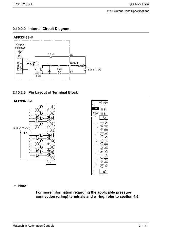
I/O AllocationFP3/FP10SH
2 − 71Matsushita Automation Controls
2.10 Output Units Specifications
2.10.2.2 Internal Circuit Diagram
Output
Internal
circuit
OutputindicatorLED
Load
5 to 24 V DC
5.6 kΩ
2 kΩ
Fuse5A
AFP33483−F
2.10.2.3 Pin Layout of Terminal Block
5 to 24 V DC
AFP33483−F
Note
For more information regarding the applicable pressureconnection (crimp) terminals and wiring, refer to section 4.5.
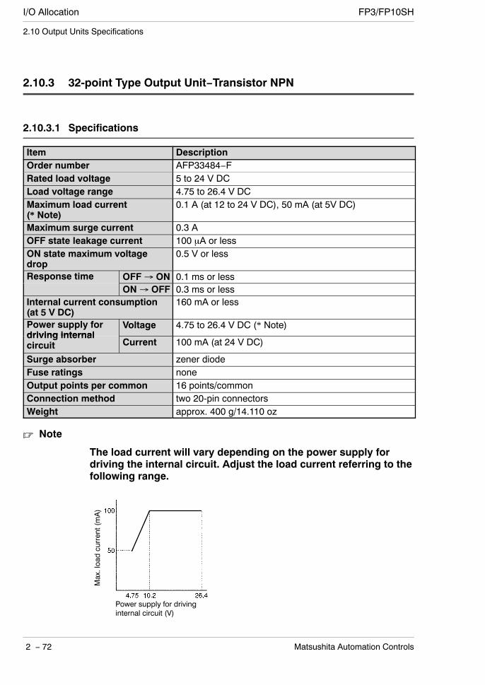
I/O Allocation FP3/FP10SH
2 − 72 Matsushita Automation Controls
2.10 Output Units Specifications
2.10.3 32-point Type Output Unit−Transistor NPN
2.10.3.1 Specifications
Item DescriptionOrder number AFP33484−FRated load voltage 5 to 24 V DCLoad voltage range 4.75 to 26.4 V DCMaximum load current(* Note)
0.1 A (at 12 to 24 V DC), 50 mA (at 5V DC)
Maximum surge current 0.3 AOFF state leakage current 100 µA or lessON state maximum voltagedrop
0.5 V or less
Response time OFF→ ON 0.1 ms or lesspON→ OFF 0.3 ms or less
Internal current consumption(at 5 V DC)
160 mA or less
Power supply fordriving internal
Voltage 4.75 to 26.4 V DC (* Note)driving internalcircuit Current 100 mA (at 24 V DC)
Surge absorber zener diodeFuse ratings noneOutput points per common 16 points/commonConnection method two 20-pin connectorsWeight approx. 400 g/14.110 oz
Note
The load current will vary depending on the power supply fordriving the internal circuit. Adjust the load current referring to thefollowing range.
Max.loadcurrent(mA)
Power supply for drivinginternal circuit (V)

I/O AllocationFP3/FP10SH
2 − 73Matsushita Automation Controls
2.10 Output Units Specifications
2.10.3.2 Internal Circuit Diagram
Output
Internal
circuit
OutputindicatorLED
Load
5 to 24 V DC
10 kΩ
10 kΩ
AFP33484−F
2.10.3.3 Pin Layout of Connector
Pin layout offirst 16 points
Pin layout oflast 16 points
5 to 24 V DC
5 to 24 V DC
I II
IV III
NotesAlthough (10A, 10B) and⊖ (9A, 9B) terminals areconnected with the same connector. It is recommended thatthey also be connected externally.For more information regarding the applicable connectors andterminals, refer to section 4.4.

I/O Allocation FP3/FP10SH
2 − 74 Matsushita Automation Controls
2.10 Output Units Specifications
2.10.4 64-point Type Output Unit−Transistor NPN
2.10.4.1 Specifications
Item DescriptionOrder number AFP33487−FRated load voltage 5 to 24 V DCLoad voltage range 4.75 to 26.4 V DCMaximum load current(* Note)
0.1 A (at 12 to 24 V DC), 50 mA (at 5 V DC)
Maximum surge current 0.3 AOFF state leakage current 100 µA or lessON state maximum voltagedrop
0.5 V or less
Response time OFF→ ON 0.1 ms or lesspON→ OFF 0.3 ms or less
Internal current consumption(at 5 V DC)
250 mA or less
Surge absorber zener diodeFuse ratings noneOutput points per common 32 points/commonConnection method two 40-pin connectorsWeight approx. 400 g/14.110 oz
Note
The load current will vary depending on the power supply fordriving the internal circuit. Adjust the load current referring to thefollowing range.
Max.loadcurrent(mA)
Power supply for drivinginternal circuit (V)
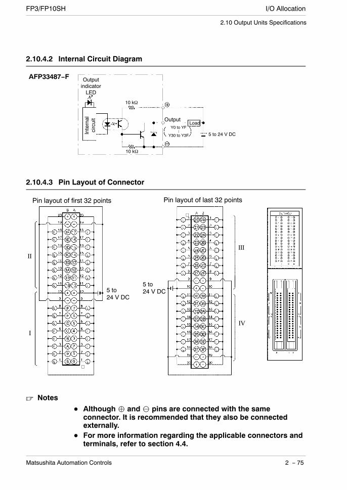
I/O AllocationFP3/FP10SH
2 − 75Matsushita Automation Controls
2.10 Output Units Specifications
2.10.4.2 Internal Circuit Diagram
Y0 to YF⋮
Y30 to Y3F
Output
Internal
circuit
OutputindicatorLED
Load
5 to 24 V DC
10 kΩ
10 kΩ
AFP33487−F
2.10.4.3 Pin Layout of Connector
III
IVI
II
Pin layout of first 32 points Pin layout of last 32 points
5 to24 V DC
∀
∀
5 to24 V DC
NotesAlthough and⊖ pins are connected with the sameconnector. It is recommended that they also be connectedexternally.For more information regarding the applicable connectors andterminals, refer to section 4.4.

I/O Allocation FP3/FP10SH
2 − 76 Matsushita Automation Controls
2.10 Output Units Specifications
2.10.5 16-point Type Output Unit−Transistor PNP
2.10.5.1 Specifications
Item DescriptionOrder number AFP33583−FRated load voltage 5 to 24 V DCLoad voltage range 4.75 to 26.4 V DCMaximum load current(* Note)
0.5 A (at 24 V DC),0.3 A (at 12 V DC),0.1 A (at 5 V DC)
Maximum surge current 5 A, 100 ms or lessOFF state leakage current 100 µA or lessON state maximum voltagedrop
0.5 V or less
Response time OFF→ ON 0.1 ms or lesspON→ OFF 0.3 ms or less
Internal current consumption(at 5 V DC)
120 mA or less
Power supply fordriving internal
Voltage 4.75 to 26.4 V DC (* Note.)driving internalcircuit Current 200 mA (at 24 V DC)
Surge absorber zener diodeFuse ratings 5 A (1 piece/common)Output points per common 8 points/commonConnection method terminal block (M 3.5 screw)Weight approx. 350 g/12.346 oz
NoteThe load current will vary depending on the power supply fordriving the internal circuit. Adjust the load current referring to thefollowing range.
Max.loadcurrent(mA)
Power supply for drivinginternal circuit (V)
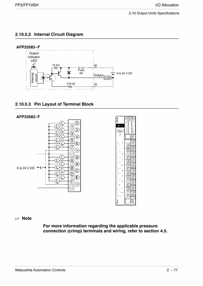
I/O AllocationFP3/FP10SH
2 − 77Matsushita Automation Controls
2.10 Output Units Specifications
2.10.5.2 Internal Circuit Diagram
Output
Internal
circuit
OutputindicatorLED
5 to 24 V DC
15 kΩ
3.9 kΩ
Fuse5A
AFP33583−F
Load
2.10.5.3 Pin Layout of Terminal Block
5 to 24 V DC
AFP33583−F
Note
For more information regarding the applicable pressureconnection (crimp) terminals and wiring, refer to section 4.5.
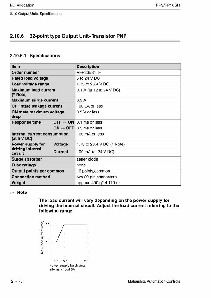
I/O Allocation FP3/FP10SH
2 − 78 Matsushita Automation Controls
2.10 Output Units Specifications
2.10.6 32-point type Output Unit−Transistor PNP
2.10.6.1 Specifications
Item DescriptionOrder number AFP33584−FRated load voltage 5 to 24 V DCLoad voltage range 4.75 to 26.4 V DCMaximum load current(* Note)
0.1 A (at 12 to 24 V DC)
Maximum surge current 0.3 AOFF state leakage current 100 µA or lessON state maximum voltagedrop
0.5 V or less
Response time OFF→ ON 0.1 ms or lesspON→ OFF 0.3 ms or less
Internal current consumption(at 5 V DC)
160 mA or less
Power supply fordriving internal
Voltage 4.75 to 26.4 V DC (* Note)driving internalcircuit Current 100 mA (at 24 V DC)
Surge absorber zener diodeFuse ratings noneOutput points per common 16 points/commonConnection method two 20-pin connectorsWeight approx. 400 g/14.110 oz
Note
The load current will vary depending on the power supply fordriving the internal circuit. Adjust the load current referring to thefollowing range.
Max.loadcurrent(mA)
Power supply for drivinginternal circuit (V)
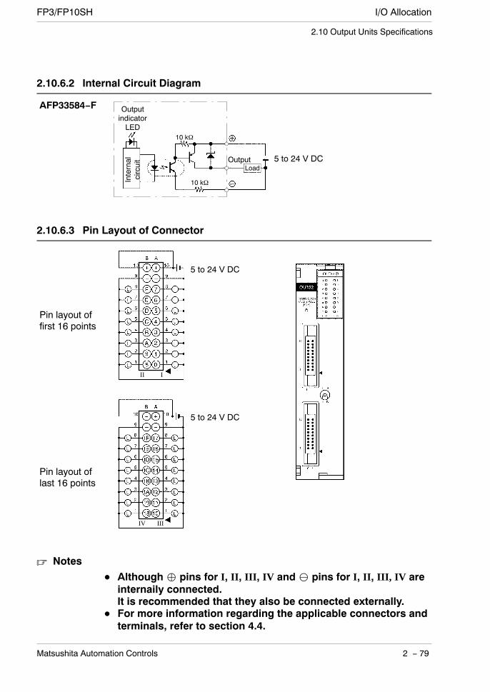
I/O AllocationFP3/FP10SH
2 − 79Matsushita Automation Controls
2.10 Output Units Specifications
2.10.6.2 Internal Circuit Diagram
5 to 24 V DCOutput
Internal
circuit
OutputindicatorLED
Load
10 kΩ
10 kΩ
AFP33584−F
2.10.6.3 Pin Layout of Connector
Pin layout offirst 16 points
Pin layout oflast 16 points
5 to 24 V DC
II I
IV III
5 to 24 V DC
NotesAlthough pins for I, II, III, IV and⊖ pins for I, II, III, IV areinternaily connected.It is recommended that they also be connected externally.For more information regarding the applicable connectors andterminals, refer to section 4.4.
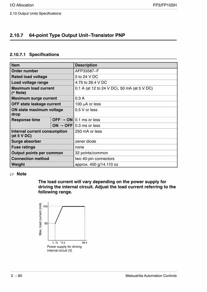
I/O Allocation FP3/FP10SH
2 − 80 Matsushita Automation Controls
2.10 Output Units Specifications
2.10.7 64-point Type Output Unit−Transistor PNP
2.10.7.1 Specifications
Item DescriptionOrder number AFP33587−FRated load voltage 5 to 24 V DCLoad voltage range 4.75 to 26.4 V DCMaximum load current(* Note)
0.1 A (at 12 to 24 V DC), 50 mA (at 5 V DC)
Maximum surge current 0.3 AOFF state leakage current 100 µA or lessON state maximum voltagedrop
0.5 V or less
Response time OFF→ ON 0.1 ms or lesspON→ OFF 0.3 ms or less
Internal current consumption(at 5 V DC)
250 mA or less
Surge absorber zener diodeFuse ratings noneOutput points per common 32 points/commonConnection method two 40-pin connectorsWeight approx. 400 g/14.110 oz
Note
The load current will vary depending on the power supply fordriving the internal circuit. Adjust the load current referring to thefollowing range.
Max.loadcurrent(mA)
Power supply for drivinginternal circuit (V)
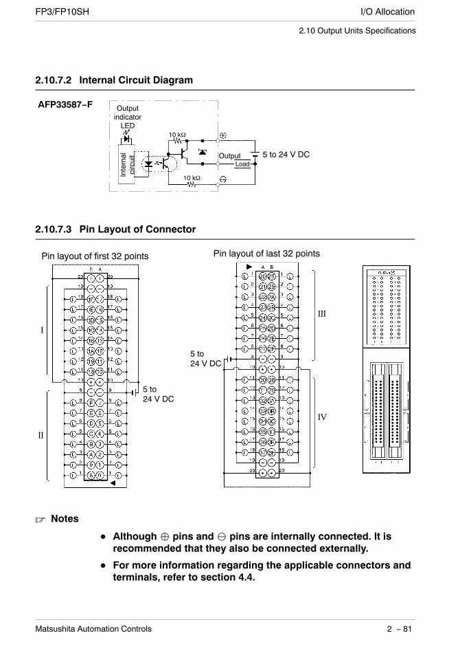
I/O AllocationFP3/FP10SH
2 − 81Matsushita Automation Controls
2.10 Output Units Specifications
2.10.7.2 Internal Circuit Diagram
5 to 24 V DCOutput
Internal
circuit
OutputindicatorLED
Load
10 kΩ
10 kΩ
AFP33587−F
2.10.7.3 Pin Layout of Connector
III
IV
I
II
Pin layout of first 32 points Pin layout of last 32 points
5 to24 V DC
5 to24 V DC
Notes
Although pins and⊖ pins are internally connected. It isrecommended that they also be connected externally.
For more information regarding the applicable connectors andterminals, refer to section 4.4.
I/O Allocation FP3/FP10SH
2 − 82 Matsushita Automation Controls
2.10 Output Units Specifications
2.10.8 16-point Type Triac Output Unit
2.10.8.1 Specifications
Item DescriptionOrder number AFP33703Rated load voltage 100 to 240 V AC, 50/60 HzLoad voltage range 85 to 264 V ACMaximum load current 0.5 A/point, 2 A/commonMaximum surge current 15 A, 100 ms or lessMinimum load current 25 mAOFF state leakage current 3 mA or less (at 240 V AC)ON state maximum voltagedrop
2.5 V or less (0.1 A or less)1.5 V or less (0.1 A to 0.5 A)
Response time OFF→ ON 1 ms or lesspON→ OFF 0.5 cycle + 1 ms or less
Internal current consumption(at 5 V DC)
200 mA or less
Surge absorber varistorFuse ratings 5 A (1 piece/common)Output points per common 8 points/commonConnection method terminal block (M 3.5 screw)Weight approx. 400 g/14.110 oz
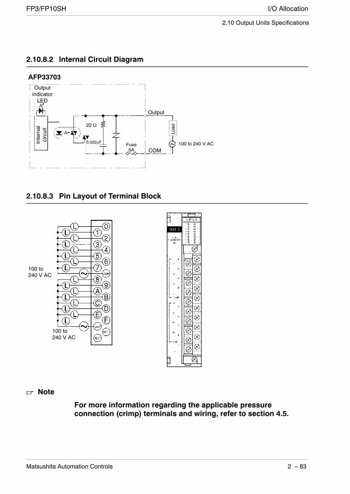
I/O AllocationFP3/FP10SH
2 − 83Matsushita Automation Controls
2.10 Output Units Specifications
2.10.8.2 Internal Circuit Diagram
Output
Internal
circuit
OutputindicatorLED
COM100 to 240 V ACFuse
5A
AFP33703
22 Ω
0.022µF
Load
2.10.8.3 Pin Layout of Terminal Block
100 to240 V AC
100 to240 V AC
Note
For more information regarding the applicable pressureconnection (crimp) terminals and wiring, refer to section 4.5.

I/O Allocation FP3/FP10SH
2 − 84 Matsushita Automation Controls
2.11 I/O Mixed Units Specifications
2.11 I/O Mixed Units Specifications
2.11.1 64−point Type I/O Mixed Unit−DC Input/Transistor NPN
2.11.1.1 Specifications
Item DescriptionOrder number AFP33428−FInput Number of input points 32 pointsput
Rated input voltage 12 to 24 V DCRated input current approx. 6.2 mA (at 24 V DC)Input impedance approx. 3.9 k ΩInput voltage range 10.2 to 26.4 V DCMin. ON voltage/Min. ONcurrent
9.6 V/3 mA
Max. OFF voltage/Max. OFFcurrent
2.5 V/1 mA
Response time OFF→ ON 0.1 ms or lesspON→ OFF 0.3 ms or less
Input points per common 32 points/commonEither the positive or negative of the input powersupply can be connected to COM (common)terminal.
Output Number of output points 32 pointspRated load voltage 5 to 24 V DCLoad voltage range 4.75 to 26.4 V DCMaximum load current 0.1 A (at 12 to 24 V DC), 50 mA (at 5 V DC)Maximum surge current 0.3 A or lessOFF state leakage current 100 µA or lessON state maximum voltagedrop
0.5 V or less
Response time OFF→ ON 0.1 ms or lesspON→ OFF 0.3 ms or less
Power supplyfor driving
Voltage 4.75 to 26.4 V DCfor drivinginternal circuit Current 100 mA (at 24 V DC)
Surge absorber zener diodeFuse ratings noneOutput points per common 32 points/common
Internal current consumption(at 5 V DC)
230 mA or less
Connection method two 40-pin connectorsWeight approx. 400 g/14.110 oz

I/O AllocationFP3/FP10SH
2 − 85Matsushita Automation Controls
2.11 I/O Mixed Units Specifications
2.11.1.2 Internal Circuit Diagram
AFP33428−FInput section (left side connector)
COM
Input
Internal
circuit
InputindicatorLED
3.9 kΩ
3.9 kΩ
1 kΩ0.1µF
12 to24 V DC
Note
Keep the rate of input points per common which aresimultaneously ON within the following range as determined bythe temperature.
100
8570
37/98.6
49/120.2
55/131
at 24 V DCat 26.4 V DC
Ambient temperature (°C/°F)
Rate of inputpoints percommonwhich aresimultaneousON (%)
Output section (right side connector)
Output
Internal
circuit
OutputindicatorLED
10 kΩ
5 to24 V DC
10 kΩ
Load
next page

I/O Allocation FP3/FP10SH
2 − 86 Matsushita Automation Controls
2.11 I/O Mixed Units Specifications
Note
The load current will vary depending on the power supply fordriving the internal circuit. Adjust the load current referring to thefollowing range.
Max.loadcurrent(mA)
Power supply for drivinginternal circuit (V)
2.11.1.3 Pin Layout of Connector
I
II
12 to24 V DC
Input section(left side connector)
Output section(right side connector)
5 to24 V DC
CN1 CN2
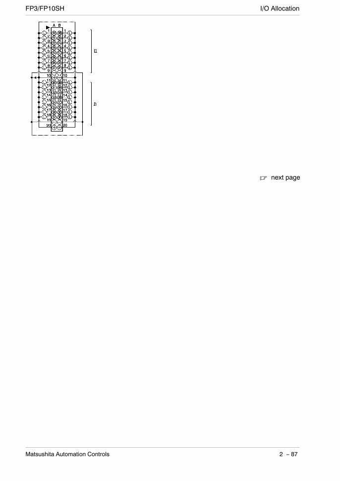
I/O AllocationFP3/FP10SH
2 − 87Matsushita Automation Controls
next page

I/O Allocation FP3/FP10SH
2 − 88 Matsushita Automation Controls
2.11 I/O Mixed Units Specifications
Notes
COM pins for I and for II are internally connected.
Although pins and⊖ pins for III and for IV are internallyconnected. It is recommended that they also be connectedexternally.
For more information regarding the applicable connectors andterminals, refer to section 4.4.

I/O AllocationFP3/FP10SH
2 − 89Matsushita Automation Controls
2.11 I/O Mixed Units Specifications
2.11.2 64−point Type I/O Mixed Unit−DC Input/Transistor PNP
2.11.2.1 Specifications
Item DescriptionOrder number AFP33528−FInput Number of input points 32 pointsput
Rated input voltage 12 to 24 V DCRated input current approx. 6.2 mA (at 24 V DC)Input impedance approx. 3.9 k ΩInput voltage range 10.2 to 26.4 V DCMin. ON voltage/Min. ONcurrent
9.6 V/3 mA
Max. OFF voltage/Max. OFFcurrent
2.5 V/1 mA
Response time OFF→ ON 0.1 ms or lesspON→ OFF 0.3 ms or less
Input points per common 32 points/commonEither the positive or negative of the input powersupply can be connected to COM (common)terminal.
Output Number of output points 32 pointspRated load voltage 5 to 24 V DCLoad voltage range 4.75 to 26.4 V DCMaximum load current 0.1 A (at 12 to 24 V DC), 50 mA (at 5 V DC)Maximum surge current 0.3 A or lessOFF state leakage current 100 µA or lessON state maximum voltagedrop
0.5 V or less
Response time OFF→ ON 0.1 ms or lesspON→ OFF 0.3 ms or less
Power supplyfor driving
Voltage 4.75 to 26.4 V DCfor drivinginternal circuit Current 100 mA (at 24 V DC)
Surge absorber zener diodeFuse ratings noneOutput points per common 32 points/common
Internal current consumption(at 5 V DC)
230 mA or less
Connection method two 40-pin connectorsWeight approx. 400 g/14.110 oz
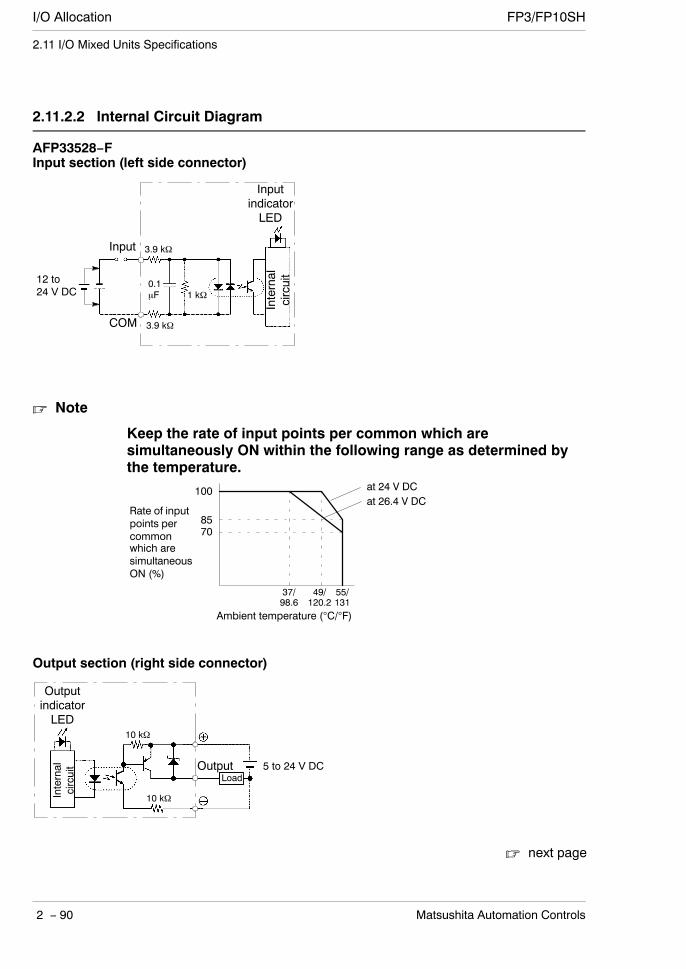
I/O Allocation FP3/FP10SH
2 − 90 Matsushita Automation Controls
2.11 I/O Mixed Units Specifications
2.11.2.2 Internal Circuit Diagram
AFP33528−FInput section (left side connector)
COM
Input
Internal
circuit
InputindicatorLED
3.9 kΩ
3.9 kΩ
1 kΩ0.1µF
12 to24 V DC
Note
Keep the rate of input points per common which aresimultaneously ON within the following range as determined bythe temperature.
100
8570
37/98.6
49/120.2
55/131
at 24 V DCat 26.4 V DC
Ambient temperature (°C/°F)
Rate of inputpoints percommonwhich aresimultaneousON (%)
Output section (right side connector)
Output
Internal
circuit
OutputindicatorLED
10 kΩ
5 to 24 V DC
10 kΩ
Load
next page
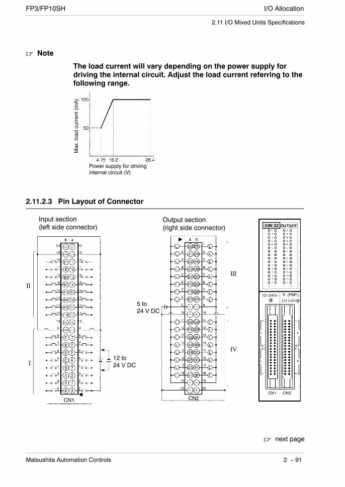
I/O AllocationFP3/FP10SH
2 − 91Matsushita Automation Controls
2.11 I/O Mixed Units Specifications
Note
The load current will vary depending on the power supply fordriving the internal circuit. Adjust the load current referring to thefollowing range.
Max.loadcurrent(mA)
Power supply for drivinginternal circuit (V)
2.11.2.3 Pin Layout of Connector
I
II
Input section(left side connector)
III
IV
Output section(right side connector)
12 to24 V DC
5 to24 V DC
CN1 CN2
next page

I/O Allocation FP3/FP10SH
2 − 92 Matsushita Automation Controls
2.11 I/O Mixed Units Specifications
Notes
COM pins for I and for II are internally connected.
Although pins and⊖ pins for III and for IV are internallyconnected. It is recommended that they also be connectedexternally.
For more information regarding the applicable connectors andterminals, refer to section 4.4.
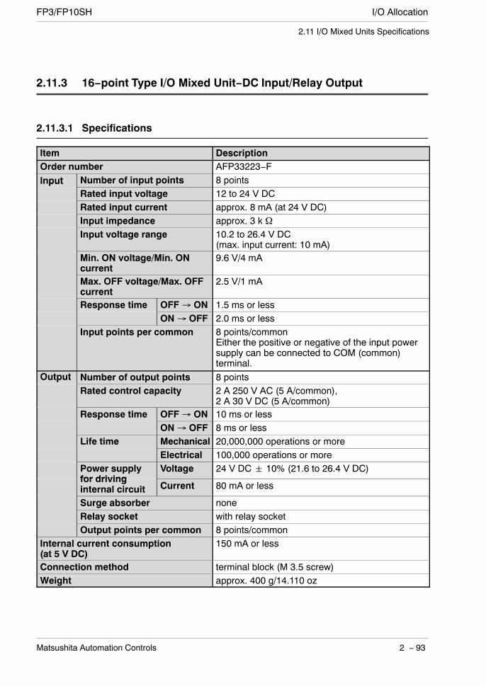
I/O AllocationFP3/FP10SH
2 − 93Matsushita Automation Controls
2.11 I/O Mixed Units Specifications
2.11.3 16−point Type I/O Mixed Unit−DC Input/Relay Output
2.11.3.1 Specifications
Item DescriptionOrder number AFP33223−FInput Number of input points 8 pointsput
Rated input voltage 12 to 24 V DCRated input current approx. 8 mA (at 24 V DC)Input impedance approx. 3 k ΩInput voltage range 10.2 to 26.4 V DC
(max. input current: 10 mA)Min. ON voltage/Min. ONcurrent
9.6 V/4 mA
Max. OFF voltage/Max. OFFcurrent
2.5 V/1 mA
Response time OFF→ ON 1.5 ms or lesspON→ OFF 2.0 ms or less
Input points per common 8 points/commonEither the positive or negative of the input powersupply can be connected to COM (common)terminal.
Output Number of output points 8 pointspRated control capacity 2 A 250 V AC (5 A/common),
2 A 30 V DC (5 A/common)Response time OFF→ ON 10 ms or lessp
ON→ OFF 8 ms or lessLife time Mechanical 20,000,000 operations or more
Electrical 100,000 operations or morePower supplyfor driving
Voltage 24 V DC 10% (21.6 to 26.4 V DC)for drivinginternal circuit Current 80 mA or less
Surge absorber noneRelay socket with relay socketOutput points per common 8 points/common
Internal current consumption(at 5 V DC)
150 mA or less
Connection method terminal block (M 3.5 screw)Weight approx. 400 g/14.110 oz

I/O Allocation FP3/FP10SH
2 − 94 Matsushita Automation Controls
2.11 I/O Mixed Units Specifications
2.11.3.2 Internal Circuit Diagram
AFP33223−F
Input
Internalcircuit
1.5 kΩ
1 kΩ
Load
24 V DC
Output
COM
Output
1.5 kΩ
0.15 µF
⊖
LED
250 V AC, 2 A30 V DC, 2 A
12 to 24 V DC
2.11.3.3 Pin Layout of Terminal Block
12 to 24 V DC
24 V DC
AFP33223−F
250 V AC, 2 A30 V DC, 2 A
Note
For more information regarding the applicable pressureconnection (crimp) terminals and wiring, refer to section 4.5.
Chapter 3
I/O Allocation
3.1 Fundamentals of I/O Allocation(Automatic Allocation) 3 − 3. . . . . . . . . . . . . . . . . . . . .
3.1.1 Example of Automatic Allocation 3 − 3. . . .
3.1.2 Using Automatic Allocation 3 − 4. . . . . . . .
3.1.3 Procedure for Automatic Allocation 3 − 5.
3.2 Arbitrary Allocation With NPST−GR 3 − 6. . . . . . . . .
3.2.1 Example of Arbitrary AllocationWith NPST−GR 3 − 6. . . . . . . . . . . . . . . . . .
3.2.2 Using Arbitrary Allocation 3 − 7. . . . . . . . . .
3.2.3 Procedure of Arbitrary Allocation 3 − 8. . .
3.3 Registration of I/O Mount Allocation 3 − 9. . . . . . . . .
3.3.1 Registration Method of Mount State 3 − 9.
3.3.1.1 Using Registration of I/OAllocation 3 − 9. . . . . . . . . . . . . . . .
3.3.1.2 Clearing RegisteredContent 3 − 10. . . . . . . . . . . . . . . . .
3.4 Table of I/O Occupied Points 3 − 11. . . . . . . . . . . . . .

I/O Allocation FP3/FP10SH
3 − 2 Matsushita Automation Controls
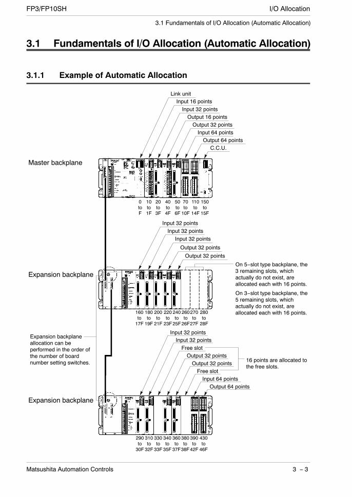
I/O AllocationFP3/FP10SH
3 − 3Matsushita Automation Controls
3.1 Fundamentals of I/O Allocation (Automatic Allocation)
3.1 Fundamentals of I/O Allocation (Automatic Allocation)
3.1.1 Example of Automatic Allocation
Master backplane
Link unitInput 16 pointsInput 32 pointsOutput 16 pointsOutput 32 pointsInput 64 pointsOutput 64 points
C.C.U.
Input 32 pointsInput 32 points
Input 32 points
Output 32 points
Output 32 points
0toF
10to1F
20to3F
40to4F
50to6F
70to10F
150to15F
110to14F
160to17F
180to19F
200to21F
220to23F
240to25F
260to26F
280to28F
270to27F
Expansion backplane
Expansion backplane
290to30F
310to32F
330to33F
340to35F
360to37F
380to38F
430to46F
390to42F
On 5−slot type backplane, the3 remaining slots, whichactually do not exist, areallocated each with 16 points.
On 3−slot type backplane, the5 remaining slots, whichactually do not exist, areallocated each with 16 points.
Input 32 pointsInput 32 pointsFree slotOutput 32 pointsOutput 32 pointsFree slotInput 64 points
Output 64 points
16 points are allocated tothe free slots.
Expansion backplaneallocation can beperformed in the order ofthe number of boardnumber setting switches.
I/O Allocation FP3/FP10SH
3 − 4 Matsushita Automation Controls
3.1 Fundamentals of I/O Allocation (Automatic Allocation)
3.1.2 Using Automatic Allocation
The I/O number is determined by the unit installation location and allocated in orderstarting from the left side (slot 0) of the master backplane.I/O points are allocated for each unit according to its own I/O occupation (* section 3.4).In the table of section 3.4, the occupied points are expressed in the following fashionfor convenience.
How to express the occupied points
I/O occupation points16, 32, 64, 128
Type of unitNil: I/O unitS: Intelligent unit
Type of I/OX: Input, Y: Output, E: without I/Os
16 points are allocated for the free slot.All backplanes, including 3- and 5-slot types, are regarded as 8-slot types, and slotswhich do not actually exist are regarded as open slots.On 5−slot type backplane, the 3 remaining slots, which actually do not exist, areallocated each with 16 points.On 3−slot type backplane, the 5 remaining slots, which actually do not exist, areallocated each with 16 points.Expansion backplane allocation can be performed in the order of the numbers of theboard number setting switches.
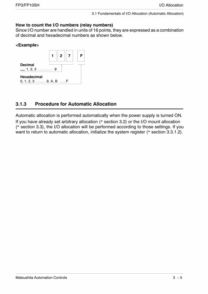
I/O AllocationFP3/FP10SH
3 − 5Matsushita Automation Controls
3.1 Fundamentals of I/O Allocation (Automatic Allocation)
How to count the I/O numbers (relay numbers)Since I/O number are handled in units of 16 points, they are expressed as a combinationof decimal and hexadecimal numbers as shown below.
Decimal, 1, 2, 3 9. . . . . . . .
Hexadecimal0, 1, 2, 3 9, A, B F. . . . . . . .
<Example>
]
7 F21
3.1.3 Procedure for Automatic Allocation
Automatic allocation is performed automatically when the power supply is turned ON.If you have already set arbitrary allocation (* section 3.2) or the I/O mount allocation(* section 3.3), the I/O allocation will be performed according to those settings. If youwant to return to automatic allocation, initialize the system register (* section 3.3.1.2).

I/O Allocation FP3/FP10SH
3 − 6 Matsushita Automation Controls
3.2 Arbitrary Allocation With NPST−GR
3.2 Arbitrary Allocation With NPST−GR
3.2.1 Example of Arbitrary Allocation With NPST−GR
Master backplane
Link unitInput 16 pointsInput 32 pointsOutput 16 pointsOutput 32 pointsInput 64 pointsOutput 64 points
C.C.U.
Input 32 pointsInput 32 points
Input 32 points
Output 32 points
Output 32 points
0toF
10to2F
30to3F
40to5F
60to9F
100to13F
140to15F
160to17F
180to19F
200to21F
220to23F
Expansion backplane
Expansion backplane
240to25F
260to27F
280to31F
320to33F
340to35F
360to39F
440to47F
400to43F
For 5-slot type backplane, thenumber of occupied I/O pointsfor the 3 slots which do notactually exist can be set to 0.(Setting: 0E) The same is truefor the 3-slot type backplanes.
Input 32 pointsInput 32 pointsFree slotOutput 32 pointsOutput 32 pointsFree slotInput 64 points
Output 64 points
You can allocato I/Opoints for units thatwill be installed in theintervening free slots.(In this example, 64points can beallocated by using the64X or 64Y setting.)
When it has not yetbeen decided whatkind of unit will beinstalled, anindeterminate numberof points can beallocated. (In thisexample, because 64points have beenallocated, a 16−point,32−point or 64−pointinput or output unitcan be selected.)
Since units such asthe C.C.U., and linkunit do not requireactual I/Os, you donot have to assignI/O points. (Setting:0SE)
I/O AllocationFP3/FP10SH
3 − 7Matsushita Automation Controls
3.2 Arbitrary Allocation With NPST−GR
3.2.2 Using Arbitrary Allocation
You have the following advantages when you use the NPST−GR software to performarbitrary allocation.For link unit and C.C.U. (computer communication unit), etc., that do not require actualI/Os, the number of I/O points can be set to 0, and the I/O numbers will be renumberedaccordingly. (Use the NPST-GR setting: 0SE).For the 5-slot type backplanes, the number of I/O points for the 3 slots which do notactually exist can be set to 0 and the I/O numbers will be renumbered accordingly.For the 3-slot type backplanes, the number of I/O points for the 5 slots which do notactually exist can be set to 0 and the I/O numbers will be renumbered accordingly.(Use the NPST-GR setting: 0E).For free slots, I/O points can be allocated for I/O units that will be installed later. Forexample, if a 32-point or 64-point unit will be added in the future, the addition of the unitwill not affect the I/O numbers for the subsequent units.When there is a possibility that the number of I/O points will increase, but the type ofunit has not yet been decided, an indeterminate number of points can be allocated.In this example, because 64 points (64Y) have been allocated in the free slot, a 16−point,32−point or 64−point output unit can be selected. The addition of the unit will not affect theI/O numbers for the subsequent units.
Note
When arbitrary allocation is not used, I/Os will be allocatedautomatically according to the automatic allocation.

I/O Allocation FP3/FP10SH
3 − 8 Matsushita Automation Controls
3.2 Arbitrary Allocation With NPST−GR
3.2.3 Procedure of Arbitrary Allocation
You can use the NPST−GR software. If you want to use NPST−GR software, read theNPST−GR manuals.
Procedure:
1. Set the NPST−GR to OFFLINE mode.
2. Press the <ESC> key to display the “NPST MENU.”Select “ALLOCATE I/O MAP” from “PLCCONFIGURATION” of the menu and press the <ESC>key.
<Settings for the example on page 3 − 6>
1. Set the number of slots to 24.(The slots will be set at 8 slotsper one backplane.)
2. Allocations will be performedfor each unit according to thesettings.
3. After the allocations are completed, register the contents of allocation bypressing the <Ctrl> and <f1> keys simultaneously. The registeredsettings can be written to the FP3/FP10SH CPU together with theprogram.The system will operate according to the I/O allocation.
Writing contents of arbitrary allocation on the NPST−GR screen1. Press the <ESC> key to display the “NPST MENU.”
2. Select “PROGRAM MANAGER” then “LOAD A PROGRAM TO PLC”,and press the <ESC> key. The program is transferred to theFP3/FP10SH CPU, and the contents of allocation are simultaneouslywritten to the FP3/FP10SH CPU as part of its system register settings.
I/O AllocationFP3/FP10SH
3 − 9Matsushita Automation Controls
3.3 Registration of I/O Mount Allocation
3.3 Registration of I/O Mount Allocation
3.3.1 Registration Method of Mount State
Registering with NPST-GRProcedure:
1. Set the mode selector of CPU to the PROG. mode andset the NPST−GR to online mode.
2. Press the <ESC> key to display the “NPST MENU.”Select “ALLOCATE I/O MAP” from the “PLCCONFIGURATION”, and press the <ENTER> key.
3. Then press <F10 (LD I/O)> key to register the currentI/O mapping.
4. Verify that “OK? (Y/N)” appears, and then press the<Y> key. By selecting “Y” in the screen, the unitcurrently mounted is read to the NPST−GR screen,and the contents of allocation are recorded to theCPU at the same time. The contents recorded at thistime are the same as the contents for automaticallocation.
Registering with FP programmer II Ver.2Perform the following key operations.The contents recorded at this time are the same as the contents for automaticallocation.
5 2 ENT WRT(−)OP
3.3.1.1 Using Registration of I/O Allocation
The registration of I/O allocation refers to the registration of the I/O numbers assignedto each unit in the system registers of the CPU.For automatic allocation (* section 3.1), the allocation depends on the state of theinstalled units when the power is turned ON. However, if the I/O allocations areregistered, the I/O numbers will not be shifted even if there are mistakes in theinstallation of the units.Arbitrary allocation (* section 3.2) is registered in the CPU at the same time the programis written, so there is no need for the registration operation.
next page
I/O Allocation FP3/FP10SH
3 − 10 Matsushita Automation Controls
3.3 Registration of I/O Mount Allocation
Notes
It is not absolutely necessary to perform the registration of I/Oallocation. If the allocation is not registered, the system willoperate according to the automatic allocations.
If the I/O allocation is registered, correct operation will not bepossible if units are changed or mount positions are changedafter registration. Redo the registration if the installationconditions do match the contents of the registration.
3.3.1.2 Clearing Registered Content
The registered content is cleared by initializing system register.Note that the contents of all the system registers will be reset when you initialize systemregister.
Clearing content using NPST-GRProcedure:
1. Set the NPST−GR to ONLINE monitor.
2. Press the <ESC> key to display the “NPST MENU.”Select “SYSTEM REGISTER” from the “PLCCONFIGURATION” of the NPST menu, and press the<ENTER> key.
3. press <F2 (INT)> key.
4. Verify that “INITIALIZE? (Y/N)” is displayed, andpress the <Y> key. The contents of the systemregister will be cleared.
Clearing content using FP programmerPerform the following key operations.
5 1 ENT WRT(−)OP
I/O AllocationFP3/FP10SH
3 − 11Matsushita Automation Controls
3.4 Table of I/O Occupied Points
3.4 Table of I/O Occupied Points
Name Ordernumber
I/O occupiedpoint
Inputunit
DC input 16-point,terminal
12 to 24 V DC AFP33023−F 16Xu t
32-point, 12 to 24 V DC AFP33024−F 32Xp ,connector 5 V DC AFP33014−F
64-point, 12 to 24 V DC AFP33027−F 64Xp ,connector AFP33028−F
24 V DC AFP33068−F
5 V DC AFP33017−F
AC input 8-point,i l
100 to 120 V AC AFP33041 16Xp p ,terminal 200 to 240 V AC AFP33051
16-point,i l
100 to 120 V AC AFP33043 16Xp ,terminal 200 to 240 V AC AFP33053
Outputi
Relay 16-point,i l
With relay socket AFP33203−F 16Ypunit
youtput
p ,terminal Without relay socket AFP33103−F
Transistor 16-point,i l
NPN open collector AFP33483−F 16Youtput
p ,terminal PNP open collector AFP33583−F
32-point, NPN open collector AFP33484−F 32Yp ,connector PNP open collector AFP33584−F
64-point, NPN open collector AFP33487−F 64Yp ,connector PNP open collector AFP33587−F
Triacoutput
16-point, terminal AFP33703 16Y
I/Omixedunit
DC input/relayoutputtype
16-point, terminal AFP33223−F 16X16Y
DC input/transistor(NPN)output
64-point, connector AFP33428−F 32X32Y
DC input/transistor(PNP)output
64-point, connector AFP33528−F 32X32Y
next page
I/O Allocation FP3/FP10SH
3 − 12 Matsushita Automation Controls
3.4 Table of I/O Occupied Points
Name Ordernumber
I/O occupiedpoint
A/D 4-channel Standard type AFP3400 16SX/converterunit
8-channel G-type AFP3402 16SE (0SE)( N )unit
yp
AFP3403
( )(* Note 1)
AFP3405
8-channel I-type AFP3406yp
AFP3407
AFP3408
D/A 2-channel Standard type AFP3410 16SX/converterunit
yp
AFP3411unit
2-channel I-type AFP3412 16SE (0SE)( N )
yp
AFP3413
( )(* Note 1)
AFP3416
AFP3417
4-channel I-type AFP3414yp
AFP3415
AFP3418
AFP3419
R.T.D. input unit AFP3420 16SX
Thermocouple input unit AFP3421 16SX
Serial data unit AFP3460 16SXSYData process unit AFP3461 16SY
High-speed counteri
1-channel type AFP3621g punit 2-channel type AFP3622
Pulse output unit AFP3480 16SX/16SY
Positioning unit E-type AFP3431E 16SX/16SYg yp
AFP3432E 32SX/32SY
Positioning unit F-type AFP3431 16SXSY
g yp
AFP3434 16SY
AFP3432 32SXSYAFP3435 32SY
AFP3436
Interrupt unit AFP3452 16SX
MEWNET-TR transmitter master unit AFP3750 0X to 128X0Y to 128Y(* Note 2)
MEWNET-F master unit AFP3742 16SE (0SE)( N )MEWNET-W link unit AFP3720
( )(* Note 1)
next page

I/O AllocationFP3/FP10SH
3 − 13Matsushita Automation Controls
3.4 Table of I/O Occupied Points
Name Ordernumber
I/O occupiedpoint
MEWNET-P link unit AFP3710 16SE (0SE)( N )C-NET link unit AFP3463
( )(* Note 1)
ET-LAN unit AFP3790
C.C.U. AFP3462
Data memory unit AFP32091 16SXy
AFP32092
Notes
(*1): The number of I/O occupied points that units marked“16SE (0SE)” possess can be set to 0 using arbitraryallocation in the NPST-GR.
(*2): I/O allocation for a MEWNET-TR transmitter master unitvary depending on the unit settings.
The occupied I/O points are expressed in the following fashionfor convenience.
I/O occupation points16, 32, 64, 128
Type of unitNil: I/O unitS: Intelligent unit
Type of I/OX: Input, Y: Output, E: without I/Os

I/O Allocation FP3/FP10SH
3 − 14 Matsushita Automation Controls
3.4 Table of I/O Occupied Points

Chapter 4
Installation and Wiring
4.1 Installation 4 − 3. . . . . . . . . . . . . . . . . . . . . . . . . . . . . .
4.1.1 Installation Space and Environment 4 − 3.
4.1.1.1 Setting the Board Number 4 − 6.
4.1.2 Mounting Method 4 − 7. . . . . . . . . . . . . . . . .
4.1.3 Connecting Expansion Cable 4 − 9. . . . . .
4.1.4 Connecting Backup Battery 4 − 10. . . . . . .
4.2 Power Supply Wiring 4 − 11. . . . . . . . . . . . . . . . . . . .
4.2.1 Wiring the Power Supply to thePower Supply Unit 4 − 11. . . . . . . . . . . . . . .
4.2.2 Grounding 4 − 13. . . . . . . . . . . . . . . . . . . . . .
4.3 Wiring Input and Output 4 − 14. . . . . . . . . . . . . . . . . .
4.3.1 Input Wiring 4 − 14. . . . . . . . . . . . . . . . . . . . .
4.3.1.1 Sensors 4 − 14. . . . . . . . . . . . . . . .
4.3.1.2 AC Input Devices 4 − 15. . . . . . . .
4.3.1.3 LED−EquippedReed Switch 4 − 15. . . . . . . . . . . .
4.3.1.4 Two−Wire Type Sensor 4 − 15. . .
4.3.1.5 LED−EquippedLimit Switch 4 − 16. . . . . . . . . . . . .
4.3.1.6 Wiring 64−pointType Input Unit 4 − 17. . . . . . . . . .
4.3.2 Output Wiring 4 − 18. . . . . . . . . . . . . . . . . . .
4.3.2.1 Protective Circuit forInductive Loads 4 − 18. . . . . . . . . .
4.3.2.2 Protective Circuit forCapacitive Loads 4 − 19. . . . . . . .
4.3.2.3 Precautions for Overload 4 − 19.
next page

I/O Allocation FP3/FP10SH
4 − 2 Matsushita Automation Controls
4.3.2.4 Precautions forLeakage Current 4 − 19. . . . . . . . .
4.3.3 Cautions Regarding Input andOutput Units 4 − 20. . . . . . . . . . . . . . . . . . . .
4.4 Wiring the Connector Type I/O Units 4 − 21. . . . . . .
4.4.1 Wiring the Connector Type Units 4 − 21. . .
4.4.2 Connecting the Terminals 4 − 24. . . . . . . . .
4.4.2.1 CT−2 Connector Terminal 4 − 24.
4.4.2.2 RT−2 Relay Terminal 4 − 27. . . . .
4.4.3 Connecting the Cable WithPressure Connection Terminal 4 − 29. . . .
4.4.4 Connecting with Connector forWire−pressed Terminal Cable 4 − 31. . . . .
4.4.5 Connecting with Flat CableConnector 4 − 33. . . . . . . . . . . . . . . . . . . . . .
4.5 Wiring the Terminal Type I/O Units 4 − 35. . . . . . . . .
4.5.1 Wiring the Terminal Type Units 4 − 35. . . .
4.6 Safety Measures 4 − 36. . . . . . . . . . . . . . . . . . . . . . . .
4.6.1 Safety Instructions 4 − 36. . . . . . . . . . . . . . .
4.6.1.1 Precautions RegardingSystem Design 4 − 36. . . . . . . . . .
4.6.1.2 Interlock Circuit 4 − 36. . . . . . . . . .
4.6.1.3 Emergency Stop Circuit 4 − 36. . .
4.6.1.4 Start Up Sequence 4 − 36. . . . . . .
4.6.1.5 Alarm Function 4 − 37. . . . . . . . . .
4.6.2 Momentary Power Failures 4 − 37. . . . . . .
4.6.3 Alarm Output 4 − 37. . . . . . . . . . . . . . . . . . .
4.6.3.1 Watchdog Timer 4 − 38. . . . . . . . .
I/O AllocationFP3/FP10SH
4 − 3Matsushita Automation Controls
4.1 Installation
4.1 Installation
4.1.1 Installation Space and Environment
DimensionsMaster backplane
AB
150/5.906
120/4.724
100/3.937
(unit: mm/in.)
Type Overall lengthA (mm/in.):
Mounting holepitchB (mm/in.):
3-slot type 260/10.236 245/9.6465-slot type 330/12.992 315/12.4028-slot type 435/17.126 420/16.535
Expansion backplane
AB
150/5.906
120/4.724
100/3.937
(unit: mm/in.)
Type Overall lengthA (mm/in.):
Mounting holepitchB (mm/in.):
3-slot type 260/10.236 245/9.6465-slot type 330/12.992 315/12.4028-slot type 435/17.126 420/16.535
I/O Allocation FP3/FP10SH
4 − 4 Matsushita Automation Controls
4.1 Installation
Installation SpaceDuck and other devices
50 mm/1.97 in. or more
50 mm/1.97 in. or more (*)
50 mm/1.97 in. or more
50 mm/1.97 in. or more
Masterbackplane
Expansionbackplane
(*): When using the MEWNET-P link unit: 80 mm/3.15 in. or more
100 mm/3.937 in. or more
Panel door, etc.
FP3/FP10SH
Other
devices
Leave at least 50 mm/1.97 in. of space between the peripheral ducts of the unit andother devices to allow heat radiation and unit replacement.Leave some further space, as indicated below, around the lower section when using alink unit.When using the MEWNET-P link unit: 80 mm/3.15 in. or moreWhen installing devices facing the FP3/FP10SH such as on the door of the panel, leavea space of at least 100 mm/3.94 in. between that device and the unit to avoid the effectsof heat or radiated noise.
next page

I/O AllocationFP3/FP10SH
4 − 5Matsushita Automation Controls
4.1 Installation
Although the depth of the unit is 120 mm/4.724 in., leave a space of at least 200mm/7.87 in. from the mounting surface for programming tool connections and wiring.
120 mm/4.724 in.
Approx. 190 mm/7.480 in.
FP peripheral cable
Avoid installing the unit in the following locations:Ambient temperatures outside the range of 0 to 55 °C/32 to 131 °F
Ambient humidity outside the range of 30 to 85 % RH
Sudden temperature changes causing condensation
Inflammable or corrosive gases
Excessive airborne dust or metal particles
Benzine, paint thinner, alcohol, other organic solvents or strong alkaline solutionssuch as ammonia or caustic soda
Excessive vibration or shock
Direct sunlight
Water in any from including spray or mist
Avoid noise interference from the following items:Influence from power transmission lines, high voltage equipment, power cables,power equipment, radio transmitters, or any other equipment that generates highswitching surges.
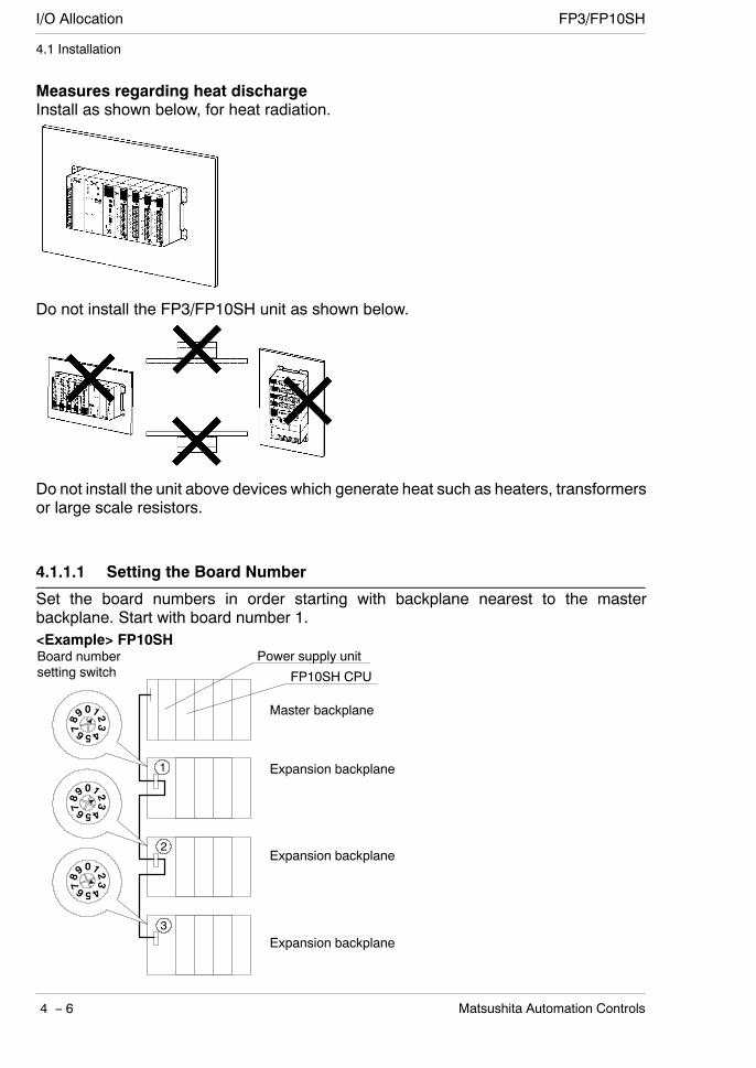
I/O Allocation FP3/FP10SH
4 − 6 Matsushita Automation Controls
4.1 Installation
Measures regarding heat dischargeInstall as shown below, for heat radiation.
Do not install the FP3/FP10SH unit as shown below.
Do not install the unit above devices which generate heat such as heaters, transformersor large scale resistors.
4.1.1.1 Setting the Board Number
Set the board numbers in order starting with backplane nearest to the masterbackplane. Start with board number 1.<Example> FP10SH
1
2
Board numbersetting switch
Power supply unit
FP10SH CPU
3
Master backplane
Expansion backplane
Expansion backplane
Expansion backplane
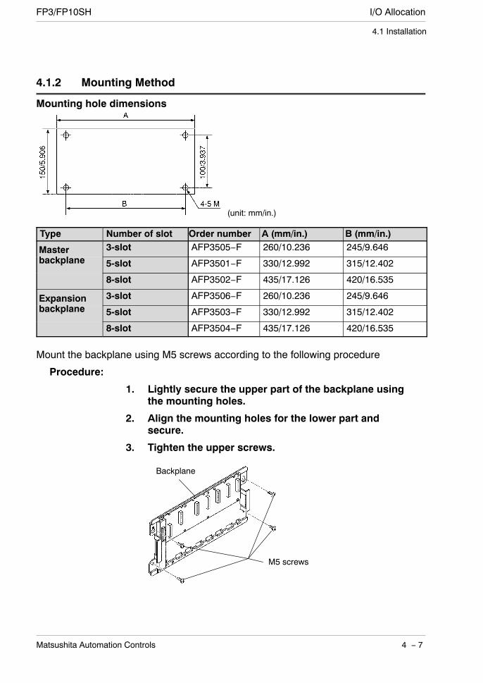
I/O AllocationFP3/FP10SH
4 − 7Matsushita Automation Controls
4.1 Installation
4.1.2 Mounting Method
Mounting hole dimensions
(unit: mm/in.)
Type Number of slot Order number A (mm/in.) B (mm/in.)
Masterb k l
3-slot AFP3505−F 260/10.236 245/9.646backplane 5-slot AFP3501−F 330/12.992 315/12.402
8-slot AFP3502−F 435/17.126 420/16.535
Expansionb k l
3-slot AFP3506−F 260/10.236 245/9.646pbackplane 5-slot AFP3503−F 330/12.992 315/12.402
8-slot AFP3504−F 435/17.126 420/16.535
Mount the backplane using M5 screws according to the following procedure
Procedure:
1. Lightly secure the upper part of the backplane usingthe mounting holes.
2. Align the mounting holes for the lower part andsecure.
3. Tighten the upper screws.
Backplane
M5 screws
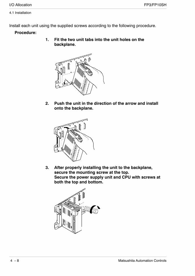
I/O Allocation FP3/FP10SH
4 − 8 Matsushita Automation Controls
4.1 Installation
Install each unit using the supplied screws according to the following procedure.
Procedure:
1. Fit the two unit tabs into the unit holes on thebackplane.
2. Push the unit in the direction of the arrow and installonto the backplane.
3. After properly installing the unit to the backplane,secure the mounting screw at the top.Secure the power supply unit and CPU with screws atboth the top and bottom.
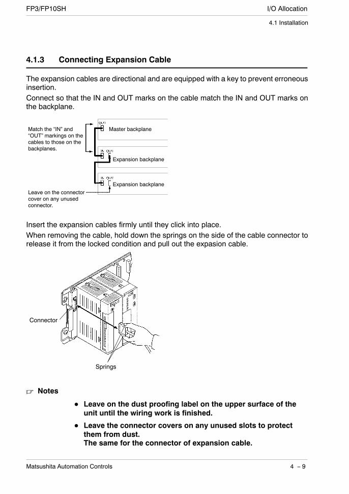
I/O AllocationFP3/FP10SH
4 − 9Matsushita Automation Controls
4.1 Installation
4.1.3 Connecting Expansion Cable
The expansion cables are directional and are equipped with a key to prevent erroneousinsertion.Connect so that the IN and OUT marks on the cable match the IN and OUT marks onthe backplane.
Master backplane
Expansion backplane
Expansion backplane
Match the “IN” and“OUT” markings on thecables to those on thebackplanes.
Leave on the connectorcover on any unusedconnector.
Insert the expansion cables firmly until they click into place.When removing the cable, hold down the springs on the side of the cable connector torelease it from the locked condition and pull out the expasion cable.
Connector
Springs
Notes
Leave on the dust proofing label on the upper surface of theunit until the wiring work is finished.
Leave the connector covers on any unused slots to protectthem from dust.The same for the connector of expansion cable.
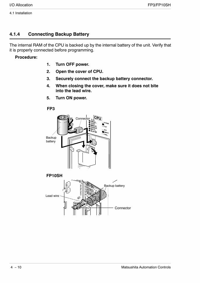
I/O Allocation FP3/FP10SH
4 − 10 Matsushita Automation Controls
4.1 Installation
4.1.4 Connecting Backup Battery
The internal RAM of the CPU is backed up by the internal battery of the unit. Verify thatit is properly connected before programming.
Procedure:
1. Turn OFF power.
2. Open the cover of CPU.
3. Securely connect the backup battery connector.
4. When closing the cover, make sure it does not biteinto the lead wire.
5. Turn ON power.
Connector
Backupbattery
FP3
Backup battery
Connector
Lead wire
FP10SH
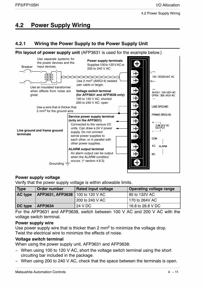
I/O AllocationFP3/FP10SH
4 − 11Matsushita Automation Controls
4.2 Power Supply Wiring
4.2 Power Supply Wiring
4.2.1 Wiring the Power Supply to the Power Supply Unit
Pin layout of power supply unit (AFP3631 is used for the example below.)
L
N
Breaker
Use separate systems forthe power devices and theinput devices.
Use an insulated transformerwhen effects from noise aregreat.
Use 2 mm2 (AWG14) twistedpair cable or larger.
Power supply terminalsSupplies100 to120VACor200 to 240 V AC
Voltage switch terminal(for AFP3631 and AFP3638 only)100 to 120 V AC: shorted200 to 240 V AC: open
Use a wire that is thicker that2 mm2 for the ground wire.
Service power supply terminal(only on the AFP3631)Connected to the various I/Ounits. Can draw a 24 V powersupply. Do not connectservie power supplies toeach other, or in parallel withother power supplies.
ALARM output terminalAn alarm output can be outputwhen the ALARM conditionoccurs. (* section 4.6.3)
Line ground and frame groundterminals
Grounding
Power supply voltageVerify that the power supply voltage is within allowable limits.Type Order number Rated input voltage Operating voltage rangeAC type AFP3631, AFP3638 100 to 120 V AC 85 to 132V ACyp ,
200 to 240 V AC 170 to 264V ACDC type AFP3634 24 V DC 16.8 to 28.8 V DCFor the AFP3631 and AFP3638, switch between 100 V AC and 200 V AC with thevoltage switch terminal.Power supply wireUse power supply wire that is thicker than 2 mm2 to minimize the voltage drop.Twist the electrical wire to minimize the effects of noise.Voltage switch terminalWhen using the power supply unit, AFP3631 and AFP3638:− When using 100 to 120 V AC, short the voltage switch terminal using the short
circuiting bar included in the package.− When using 200 to 240 V AC, check that the space between the terminals is open.
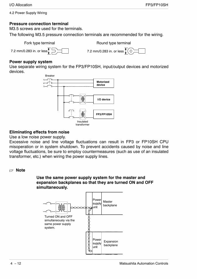
I/O Allocation FP3/FP10SH
4 − 12 Matsushita Automation Controls
4.2 Power Supply Wiring
Pressure connection terminalM3.5 screws are used for the terminals.The following M3.5 pressure connection terminals are recommended for the wiring.
7.2 mm/0.283 in. or less 7.2 mm/0.283 in. or less
Fork type terminal Round type terminal
Power supply systemUse separate wiring system for the FP3/FP10SH, input/output devices and motorizeddevices.
Breaker
Motorizeddevice
I/O device
FP3/FP10SH
Insulatedtransformer
Eliminating effects from noiseUse a low noise power supply.Excessive noise and line voltage fluctuations can result in FP3 or FP10SH CPUmisoperation or in system shutdown. To prevent accidents caused by noise and linevoltage fluctuations, be sure to employ countermeasures (such as use of an insulatedtransformer, etc.) when wiring the power supply lines.
Note
Use the same power supply system for the master andexpansion backplanes so that they are turned ON and OFFsimultaneously.
Powersupplyunit
Powersupplyunit
Turned ON and OFFsimultaneously via thesame power supplysystem.
Masterbackplane
Expansionbackplane
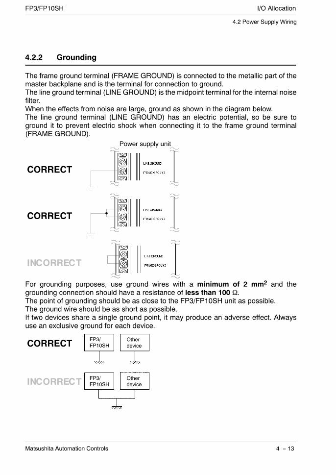
I/O AllocationFP3/FP10SH
4 − 13Matsushita Automation Controls
4.2 Power Supply Wiring
4.2.2 Grounding
The frame ground terminal (FRAME GROUND) is connected to the metallic part of themaster backplane and is the terminal for connection to ground.The line ground terminal (LINE GROUND) is the midpoint terminal for the internal noisefilter.When the effects from noise are large, ground as shown in the diagram below.The line ground terminal (LINE GROUND) has an electric potential, so be sure toground it to prevent electric shock when connecting it to the frame ground terminal(FRAME GROUND).
CORRECT
Power supply unit
CORRECT
For grounding purposes, use ground wires with a minimum of 2 mm2 and thegrounding connection should have a resistance of less than 100 Ω.The point of grounding should be as close to the FP3/FP10SH unit as possible.The ground wire should be as short as possible.If two devices share a single ground point, it may produce an adverse effect. Alwaysuse an exclusive ground for each device.
FP3/FP10SH
Otherdevice
FP3/FP10SH
CORRECT
Otherdevice
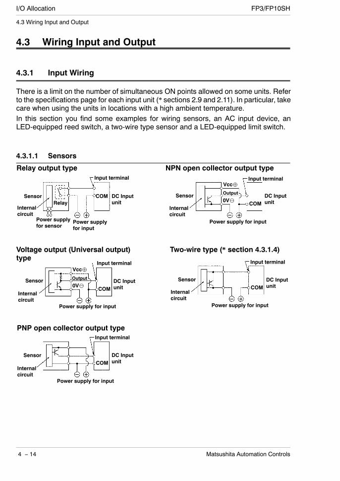
I/O Allocation FP3/FP10SH
4 − 14 Matsushita Automation Controls
4.3 Wiring Input and Output
4.3 Wiring Input and Output
4.3.1 Input Wiring
There is a limit on the number of simultaneous ON points allowed on some units. Referto the specifications page for each input unit (* sections 2.9 and 2.11). In particular, takecare when using the units in locations with a high ambient temperature.In this section you find some examples for wiring sensors, an AC input device, anLED-equipped reed switch, a two-wire type sensor and a LED-equipped limit switch.
4.3.1.1 Sensors
COM DC Inputunit
Input terminal
Power supplyfor input
Power supplyfor sensor
Sensor
Internalcircuit
Relay output type
COMDC Inputunit
Input terminal
Power supply for input
Sensor
Internalcircuit
Vcc
0V⊖
NPN open collector output type
Relay
Output
COMDC Inputunit
Input terminal
Power supply for input
Sensor
Internalcircuit
Two-wire type (* section 4.3.1.4)
COMDC Inputunit
Input terminal
Power supply for input
Sensor
Internalcircuit
Vcc
0V⊖
Voltage output (Universal output)type
Output
COMDC Inputunit
Input terminal
Power supply for input
Sensor
Internalcircuit
PNP open collector output type

I/O AllocationFP3/FP10SH
4 − 15Matsushita Automation Controls
4.3 Wiring Input and Output
4.3.1.2 AC Input Devices
COM
Inputterminal
Powersupply
COM
Inputterminal
Powersupply
ACinputdevice
Non-contact output typeContact output type
Inputunit
ACinputdevice
InputunitContact
4.3.1.3 LED−Equipped Reed Switch
When a LED is connected to an input contact such as LED-equipped reed switch, makesure that the voltage value applied to the input terminal of FP3/FP10SH is greater thanON voltage value.In particular, take care when connecting a number of switches in series.
DCinput unit
COM
Inputterminal
LED−equippedreed switch
ON voltagevalue or more
LED
Con−tact
Power supply for input
4.3.1.4 Two−Wire Type Sensor
If the input of FP3/10SH is not turned OFF because of leakage current from thetwo−wire type sensor, the use of a bleeder resistor is recommended, as shown below.
DCinput unit
Using 12 to 24 V DC type input unit(OFF voltage: 2.5 V, Input impedance: 3 kΩ)
COM
Input terminal
Two−wiretype sensor
Internalcircuit
Bleederresistor R
I: Sensor’s leakage current (mA)R: Bleeder resistor (kΩ)
Power supply for input
next page
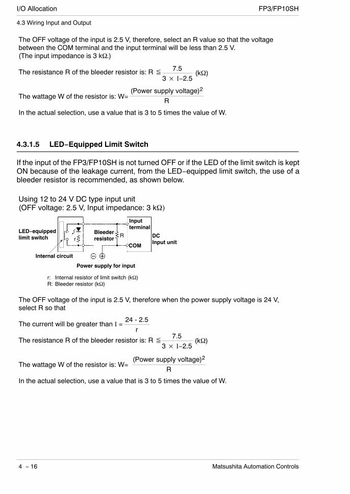
I/O Allocation FP3/FP10SH
4 − 16 Matsushita Automation Controls
4.3 Wiring Input and Output
The OFF voltage of the input is 2.5 V, therefore, select an R value so that the voltagebetween the COM terminal and the input terminal will be less than 2.5 V.(The input impedance is 3 kΩ.)
The resistance R of the bleeder resistor is: R≦
The wattage W of the resistor is: W=
In the actual selection, use a value that is 3 to 5 times the value of W.
7.53× I−2.5
(Power supply voltage)2
R
(kΩ)
4.3.1.5 LED−Equipped Limit Switch
If the input of the FP3/FP10SH is not turned OFF or if the LED of the limit switch is keptON because of the leakage current, from the LED−equipped limit switch, the use of ableeder resistor is recommended, as shown below.
The OFF voltage of the input is 2.5 V, therefore when the power supply voltage is 24 V,select R so that
The current will be greater than I =
The resistance R of the bleeder resistor is: R≦
The wattage W of the resistor is: W=
In the actual selection, use a value that is 3 to 5 times the value of W.
24 - 2.5r
Internal circuit
Using 12 to 24 V DC type input unit(OFF voltage: 2.5 V, Input impedance: 3 kΩ)
DCInput unit
COM
Inputterminal
LED−equippedlimit switch
Bleederresistor R
r
r: Internal resistor of limit switch (kΩ)R: Bleeder resistor (kΩ)
7.53× I−2.5
(Power supply voltage)2
R
(kΩ)
Power supply for input
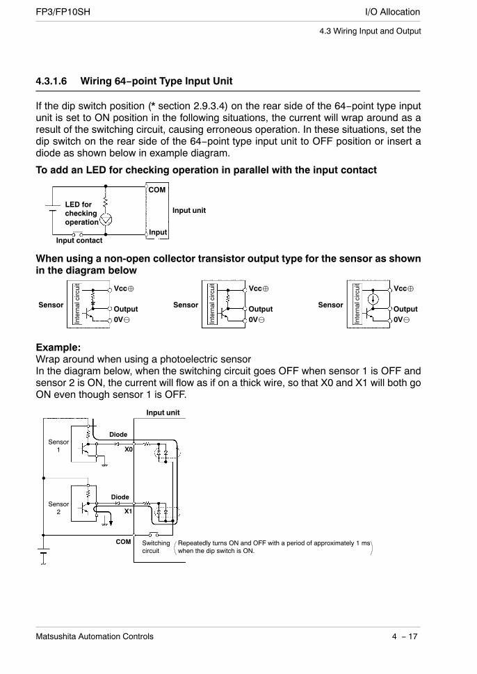
I/O AllocationFP3/FP10SH
4 − 17Matsushita Automation Controls
4.3 Wiring Input and Output
4.3.1.6 Wiring 64−point Type Input Unit
If the dip switch position (* section 2.9.3.4) on the rear side of the 64−point type inputunit is set to ON position in the following situations, the current will wrap around as aresult of the switching circuit, causing erroneous operation. In these situations, set thedip switch on the rear side of the 64−point type input unit to OFF position or insert adiode as shown below in example diagram.
To add an LED for checking operation in parallel with the input contact
COM
LED forcheckingoperation
Input unit
InputInput contact
When using a non-open collector transistor output type for the sensor as shownin the diagram below
Vcc
Internalcircuit
Output0V⊖ In
ternalcircuit
Internalcircuit
Sensor
Vcc
Output0V⊖
Sensor
Vcc
Output0V⊖
Sensor
Example:Wrap around when using a photoelectric sensorIn the diagram below, when the switching circuit goes OFF when sensor 1 is OFF andsensor 2 is ON, the current will flow as if on a thick wire, so that X0 and X1 will both goON even though sensor 1 is OFF.
Diode
Diode
COM
Input unit
Switchingcircuit
Sensor1
Sensor2
X0
X1
Repeatedly turns ON and OFF with a period of approximately 1 mswhen the dip switch is ON.
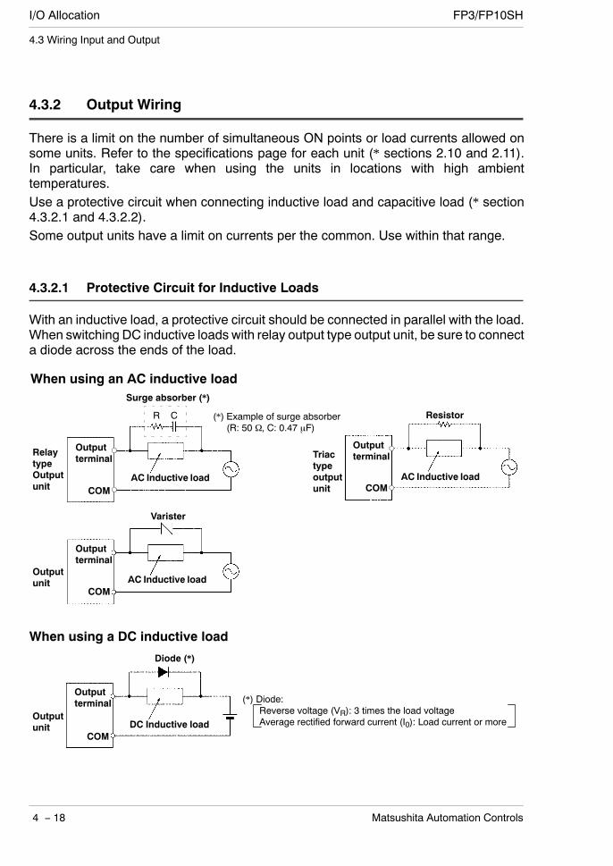
I/O Allocation FP3/FP10SH
4 − 18 Matsushita Automation Controls
4.3 Wiring Input and Output
4.3.2 Output Wiring
There is a limit on the number of simultaneous ON points or load currents allowed onsome units. Refer to the specifications page for each unit (* sections 2.10 and 2.11).In particular, take care when using the units in locations with high ambienttemperatures.Use a protective circuit when connecting inductive load and capacitive load (* section4.3.2.1 and 4.3.2.2).Some output units have a limit on currents per the common. Use within that range.
4.3.2.1 Protective Circuit for Inductive Loads
With an inductive load, a protective circuit should be connected in parallel with the load.When switching DC inductive loads with relay output type output unit, be sure to connecta diode across the ends of the load.
When using an AC inductive load
RelaytypeOutputunit COM
Outputterminal
(*) Example of surge absorber(R: 50 Ω, C: 0.47 µF)
Surge absorber (*)
AC Inductive load
R C
Varister
Outputunit
COM
Outputterminal
AC Inductive load
Triactypeoutputunit
Resistor
COM
Outputterminal
AC Inductive load
Diode (*)
When using a DC inductive load
Outputunit
COM
Outputterminal
DC Inductive loadReverse voltage (VR): 3 times the load voltageAverage rectified forward current (I0): Load current or more
(*) Diode:
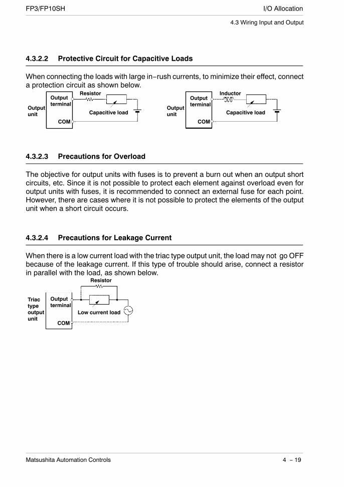
I/O AllocationFP3/FP10SH
4 − 19Matsushita Automation Controls
4.3 Wiring Input and Output
4.3.2.2 Protective Circuit for Capacitive Loads
When connecting the loads with large in−rush currents, to minimize their effect, connecta protection circuit as shown below.
Outputunit
COM
Outputterminal
Capacitive load
Resistor
Outputunit
COM
Outputterminal
Inductor
Capacitive load
4.3.2.3 Precautions for Overload
The objective for output units with fuses is to prevent a burn out when an output shortcircuits, etc. Since it is not possible to protect each element against overload even foroutput units with fuses, it is recommended to connect an external fuse for each point.However, there are cases where it is not possible to protect the elements of the outputunit when a short circuit occurs.
4.3.2.4 Precautions for Leakage Current
When there is a low current load with the triac type output unit, the load may not go OFFbecause of the leakage current. If this type of trouble should arise, connect a resistorin parallel with the load, as shown below.
Triactypeoutputunit
COM
Outputterminal
Resistor
Low current load

I/O Allocation FP3/FP10SH
4 − 20 Matsushita Automation Controls
4.3 Wiring Input and Output
4.3.3 Cautions Regarding Input and Output Units
WiringArrange the wiring so that the input and output wiring are separated, and so that theinput and output wiring is separated from the motorized wiring, as so much as possible.Do not route them through the same duct or wrap them up together.Separate the wires of input/output from the motorized and high voltage wires by at least100 mm/3.937 in.
Unit coverAttach and remove the cover of the input and output unit as shown below.The unit cover cannot be attached when using the connector for wire−pressed terminalcable with hood cover in the connector type unit.
Unit cover
Dust proofing labelDo not remove the dust proofing label that is attached to the upper portion of the unituntil the installation and wiring are finished.Be sure to remove the dust proofing label prior to operation to allow heat radiation.
Dust proofing label
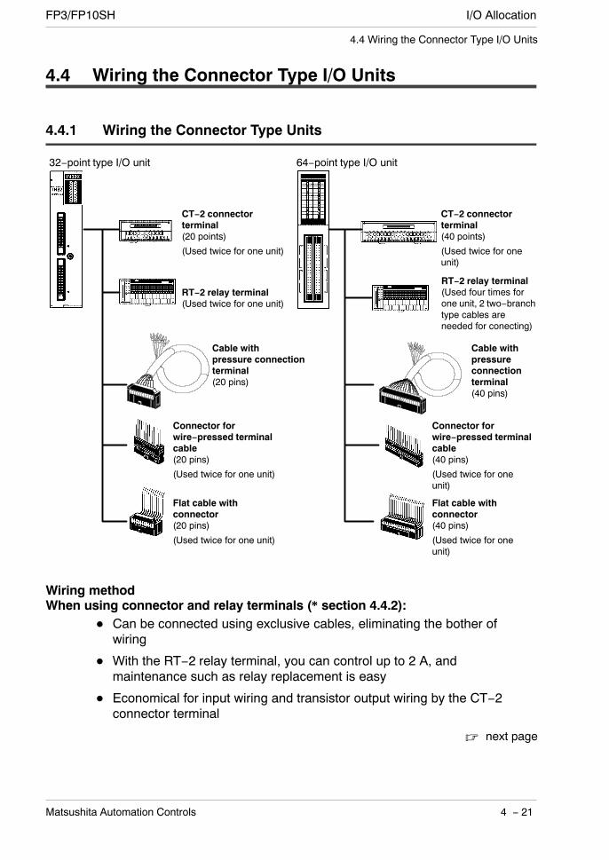
I/O AllocationFP3/FP10SH
4 − 21Matsushita Automation Controls
4.4 Wiring the Connector Type I/O Units
4.4 Wiring the Connector Type I/O Units
4.4.1 Wiring the Connector Type Units
32−point type I/O unit 64−point type I/O unit
CT−2 connectorterminal(20 points)
(Used twice for one unit)
RT−2 relay terminal(Used twice for one unit)
Cable withpressure connectionterminal(20 pins)
Connector forwire−pressed terminalcable(20 pins)
(Used twice for one unit)
Flat cable withconnector(20 pins)
(Used twice for one unit)
CT−2 connectorterminal(40 points)
(Used twice for oneunit)
RT−2 relay terminal(Used four times forone unit, 2 two−branchtype cables areneeded for conecting)
Cable withpressureconnectionterminal(40 pins)
Connector forwire−pressed terminalcable(40 pins)
(Used twice for oneunit)
Flat cable withconnector(40 pins)
(Used twice for oneunit)
Wiring methodWhen using connector and relay terminals (* section 4.4.2):
Can be connected using exclusive cables, eliminating the bother ofwiring
With the RT−2 relay terminal, you can control up to 2 A, andmaintenance such as relay replacement is easy
Economical for input wiring and transistor output wiring by the CT−2connector terminal
next page

I/O Allocation FP3/FP10SH
4 − 22 Matsushita Automation Controls
4.4 Wiring the Connector Type I/O Units
When using cable with pressure connection terminal (* section 4.4.3)The connector converted to a pressure connection terminal using theconnector terminal cable.
The correspondence between the I/O numbers and pressure connectionterminal pin numbers are the same as for connector terminals. (* section4.4.2)
When using connector for wire−pressed terminal cable (* section 4.4.4)You can directly connect wires from 0.2 to 0.3 mm2.
Eliminates the bother of wiring connections because the wires can beconnected without removing the covers from the wires.
Can correct wiring mistakes smoothly.
A tool exclusively designed for this purpose is necessary.
When using flat cable (* section 4.4.5)There is a cable with a connector on only one end.
When using a commercially available flat cable, be sure to use a suitableconnector.
next page

I/O AllocationFP3/FP10SH
4 − 23Matsushita Automation Controls
4.4 Wiring the Connector Type I/O Units
Type of unit 32-pointtypeInput unit
32-pointtypeOutput unit
64-pointtypeInput unit
64-pointtypeOutput unit
64-point typeI/O mixed unit
AFP33024−FAFP33014−F
AFP33484−FAFP33584−F(*Note 1)
AFP33027−FAFP33017−FAFP33028−FAFP F
AFP33487−FAFP33587−F(*Note 1)
AFP33428−FAFP33528−F(*Note 1)( )
AFP33068−F( )
Input Output
Number of connector pins 20 40 40
Usingterminal
CT−2connectort i l
DIN rail mountingtype
AYC1120 AYC1140 AYC1140terminal connector
terminal Direct mountingtype
AVC2120 AYC2140 AYC2140
Exclusivecable
1 m/3.281ft
AYT51203 AYT51403 AYT51403cable
2 m/6.562ft
AYT51205 AYT51405 AYT51405
RT−2 relayterminal
DIN rail mountingtype
− AY232502 − AY232502 − AY232502terminal
Direct mountingtype
− AY232522 − AY232522 − AY232522
Exclusivecable
1 m/3.281ft
− AY15133 − AY15633 − AY15633cable
2 m/6.562ft
− AY15135 − AY15635 − AY15635
Using cablewithpressure
1 m/3.281ft AYT58203 AYT58403 AYT58403
pressureconnectionterminal
2 m/6.562ft AYT58205 AYT58405 AYT58405
Using connector forwire−pressed terminalbl
Housing AXW1204A(2 pieces)
AXW1404A(2 pieces)
AXW1404A(2 pieces)wire pressed terminal
cable Contact AXW7221 (2 pieces)(5 pins/line) (*Note 2)
AXW7221 (4 pieces)(5 pins/line) (*Note 2)
Semi-cover AXW62001A(2 pieces)
AXW64001A(2 pieces)
AXW64001A(2 pieces)
Pressureconnector tool
AXY52000
Using flatcable
Flat cable with aconnector on one end
1 m/3.281ft
− − AFB8541 AFB8541cable connector on one end
2 m/6.562ft
− − AFB8542 AFB8542
Connector only AXM120415 AXM140415 AXM140415
Notes
(*1): The RT−2 relay terminal cannot be used in the PNP opencollector output type units AFP33584−F, AFP33587−F, andAFP33528−F.
(*2): When ordering, please contact your dealer regarding theminimum quantity.
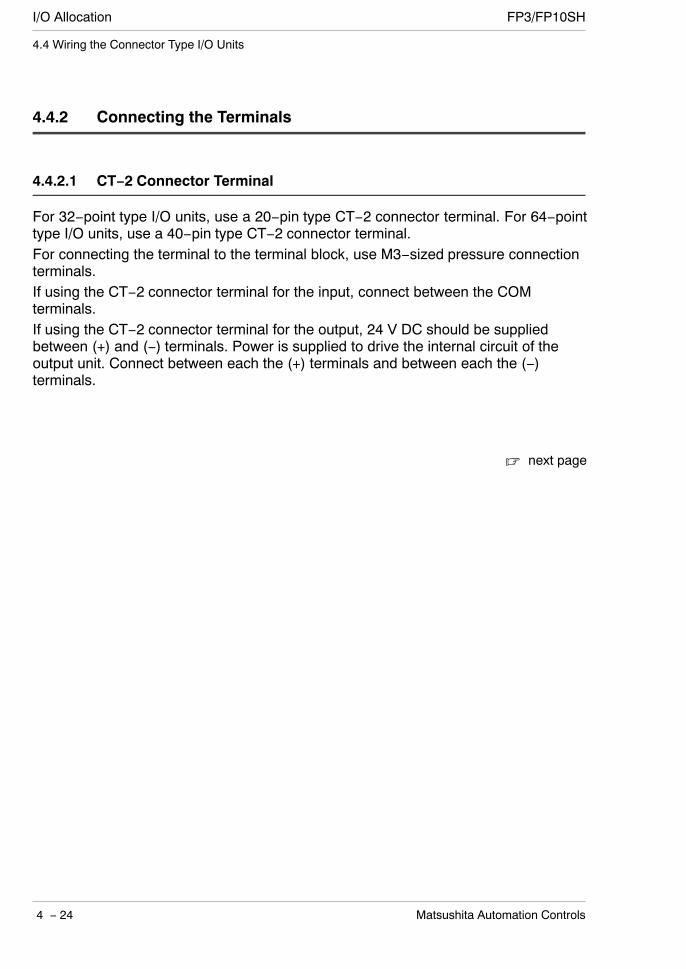
I/O Allocation FP3/FP10SH
4 − 24 Matsushita Automation Controls
4.4 Wiring the Connector Type I/O Units
4.4.2 Connecting the Terminals
4.4.2.1 CT−2 Connector Terminal
For 32−point type I/O units, use a 20−pin type CT−2 connector terminal. For 64−pointtype I/O units, use a 40−pin type CT−2 connector terminal.For connecting the terminal to the terminal block, use M3−sized pressure connectionterminals.If using the CT−2 connector terminal for the input, connect between the COMterminals.If using the CT−2 connector terminal for the output, 24 V DC should be suppliedbetween (+) and (−) terminals. Power is supplied to drive the internal circuit of theoutput unit. Connect between each the (+) terminals and between each the (−)terminals.
next page
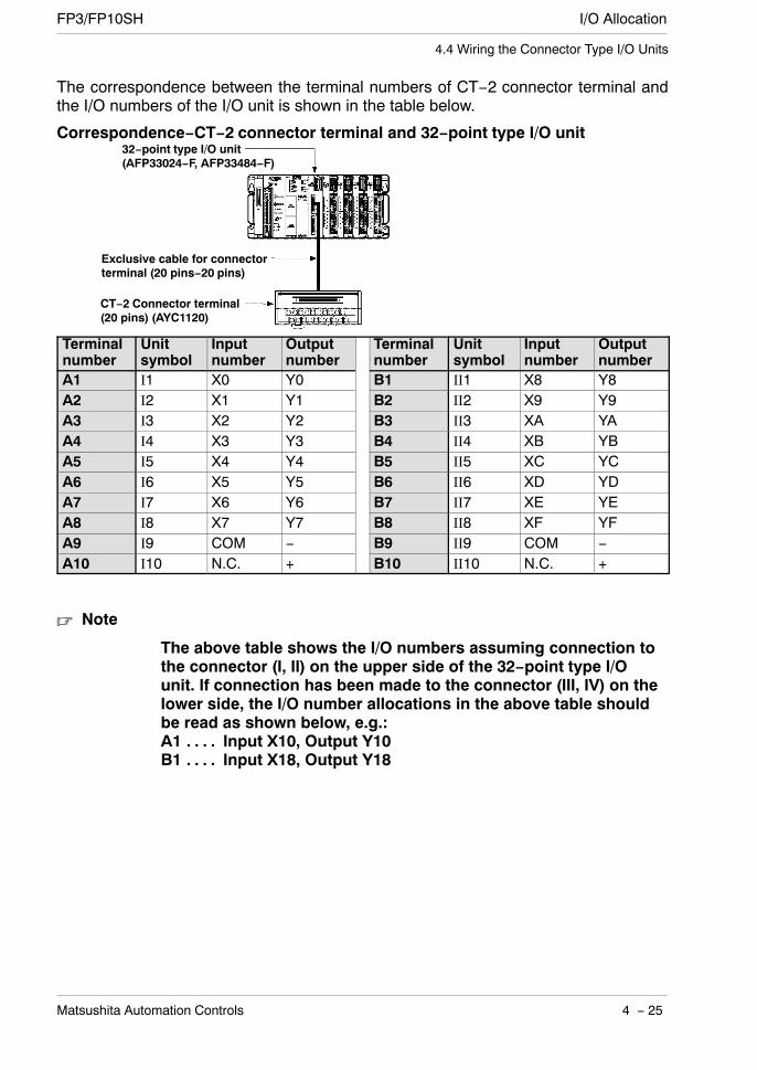
I/O AllocationFP3/FP10SH
4 − 25Matsushita Automation Controls
4.4 Wiring the Connector Type I/O Units
The correspondence between the terminal numbers of CT−2 connector terminal andthe I/O numbers of the I/O unit is shown in the table below.
Correspondence−CT−2 connector terminal and 32−point type I/O unit32−point type I/O unit(AFP33024−F, AFP33484−F)
Exclusive cable for connectorterminal (20 pins−20 pins)
CT−2 Connector terminal(20 pins) (AYC1120)
Terminalnumber
Unitsymbol
Inputnumber
Outputnumber
Terminalnumber
Unitsymbol
Inputnumber
Outputnumber
A1 I1 X0 Y0 B1 II1 X8 Y8A2 I2 X1 Y1 B2 II2 X9 Y9A3 I3 X2 Y2 B3 II3 XA YAA4 I4 X3 Y3 B4 II4 XB YBA5 I5 X4 Y4 B5 II5 XC YCA6 I6 X5 Y5 B6 II6 XD YDA7 I7 X6 Y6 B7 II7 XE YEA8 I8 X7 Y7 B8 II8 XF YFA9 I9 COM − B9 II9 COM −A10 I10 N.C. + B10 II10 N.C. +
Note
The above table shows the I/O numbers assuming connection tothe connector (I, II) on the upper side of the 32−point type I/Ounit. If connection has been made to the connector (III, IV) on thelower side, the I/O number allocations in the above table shouldbe read as shown below, e.g.:A1 Input X10, Output Y10. . . .B1 Input X18, Output Y18. . . .
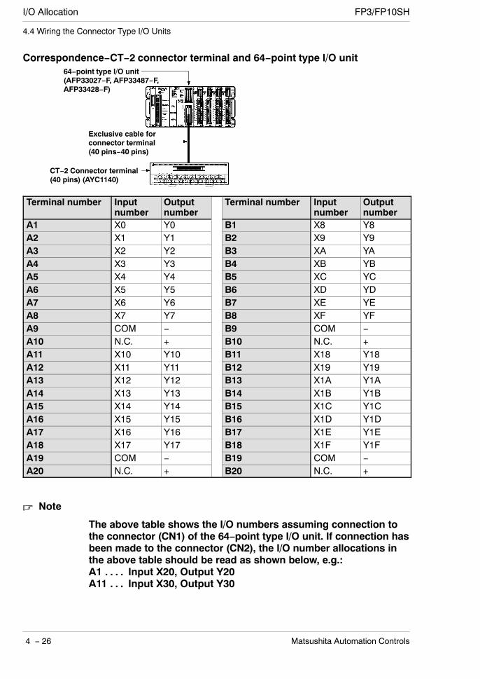
I/O Allocation FP3/FP10SH
4 − 26 Matsushita Automation Controls
4.4 Wiring the Connector Type I/O Units
Correspondence−CT−2 connector terminal and 64−point type I/O unit64−point type I/O unit(AFP33027−F, AFP33487−F,AFP33428−F)
Exclusive cable forconnector terminal(40 pins−40 pins)
CT−2 Connector terminal(40 pins) (AYC1140)
Terminal number Inputnumber
Outputnumber
Terminal number Inputnumber
Outputnumber
A1 X0 Y0 B1 X8 Y8A2 X1 Y1 B2 X9 Y9A3 X2 Y2 B3 XA YAA4 X3 Y3 B4 XB YBA5 X4 Y4 B5 XC YCA6 X5 Y5 B6 XD YDA7 X6 Y6 B7 XE YEA8 X7 Y7 B8 XF YFA9 COM − B9 COM −A10 N.C. + B10 N.C. +A11 X10 Y10 B11 X18 Y18A12 X11 Y11 B12 X19 Y19A13 X12 Y12 B13 X1A Y1AA14 X13 Y13 B14 X1B Y1BA15 X14 Y14 B15 X1C Y1CA16 X15 Y15 B16 X1D Y1DA17 X16 Y16 B17 X1E Y1EA18 X17 Y17 B18 X1F Y1FA19 COM − B19 COM −A20 N.C. + B20 N.C. +
Note
The above table shows the I/O numbers assuming connection tothe connector (CN1) of the 64−point type I/O unit. If connection hasbeen made to the connector (CN2), the I/O number allocations inthe above table should be read as shown below, e.g.:A1 Input X20, Output Y20. . . .A11 Input X30, Output Y30. . .
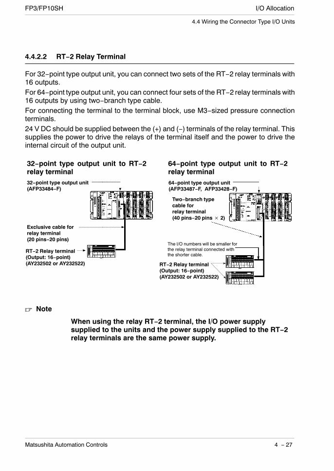
I/O AllocationFP3/FP10SH
4 − 27Matsushita Automation Controls
4.4 Wiring the Connector Type I/O Units
4.4.2.2 RT−2 Relay Terminal
For 32−point type output unit, you can connect two sets of the RT−2 relay terminals with16 outputs.For 64−point type output unit, you can connect four sets of the RT−2 relay terminals with16 outputs by using two−branch type cable.For connecting the terminal to the terminal block, use M3−sized pressure connectionterminals.24 V DC should be supplied between the (+) and (−) terminals of the relay terminal. Thissupplies the power to drive the relays of the terminal itself and the power to drive theinternal circuit of the output unit.
32−point type output unit(AFP33484−F)
Exclusive cable forrelay terminal(20 pins−20 pins)
RT−2 Relay terminal(Output: 16−point)(AY232502 or AY232522)
32−point type output unit to RT−2relay terminal
64−point type output unit to RT−2relay terminal
Two−branch typecable forrelay terminal(40 pins−20 pins× 2)
RT−2 Relay terminal(Output: 16−point)(AY232502 or AY232522)
The I/O numbers will be smaller forthe relay terminal connected withthe shorter cable.
64−point type output unit(AFP33487−F, AFP33428−F)
Note
When using the relay RT−2 terminal, the I/O power supplysupplied to the units and the power supply supplied to the RT−2relay terminals are the same power supply.

I/O Allocation FP3/FP10SH
4 − 28 Matsushita Automation Controls
4.4 Wiring the Connector Type I/O Units
Correspondence−RT−2 relay terminal and I/O unit
The correspondence between the terminal numbers of RT−2 relay terminal and the I/Onumbers of the I/O unit is shown in the table below. The output terminals have fourpoints per common.
Terminalnumber
Output number Terminalnumber
Output number
0+ Y0 8+ Y81+ Y1 9+ Y92+ Y2 A+ YA3+ Y3 B+ YBCOM− Common terminal for
Y0 to Y3COM− Common terminal for
Y8 to YB4+ Y4 C+ YC5+ Y5 D+ YD6+ Y6 E+ YE7+ Y7 F+ YFCOM− Common terminal for
Y4 to Y7COM− Common terminal for
YC to YF
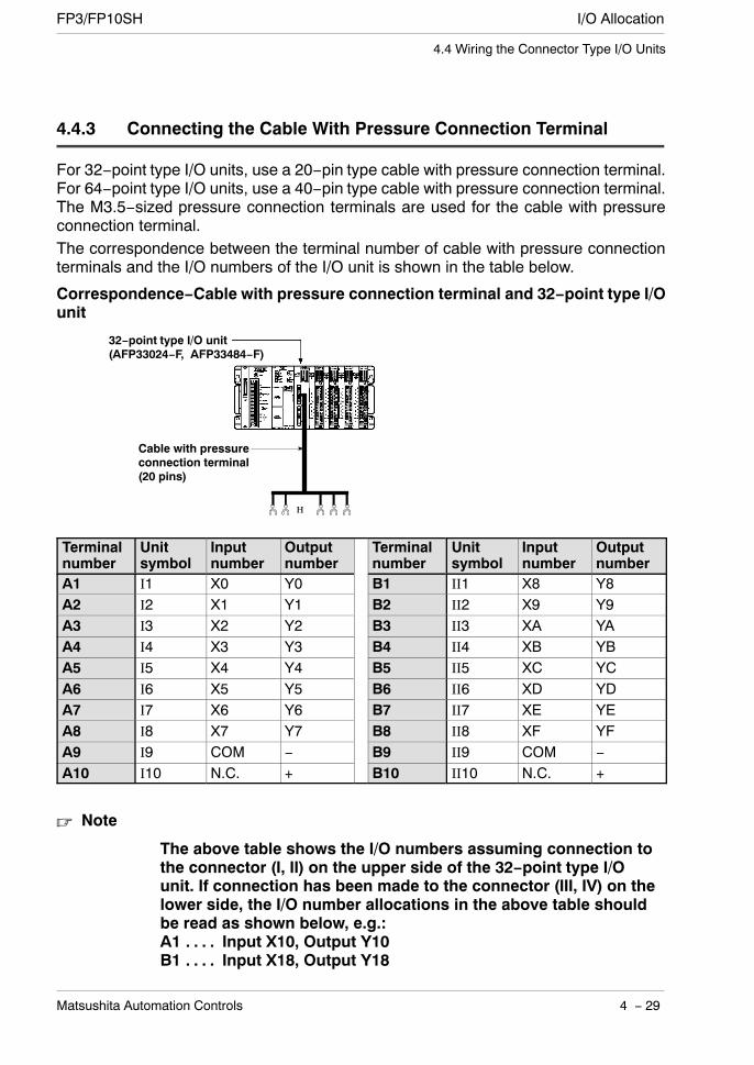
I/O AllocationFP3/FP10SH
4 − 29Matsushita Automation Controls
4.4 Wiring the Connector Type I/O Units
4.4.3 Connecting the Cable With Pressure Connection Terminal
For 32−point type I/O units, use a 20−pin type cable with pressure connection terminal.For 64−point type I/O units, use a 40−pin type cable with pressure connection terminal.The M3.5−sized pressure connection terminals are used for the cable with pressureconnection terminal.The correspondence between the terminal number of cable with pressure connectionterminals and the I/O numbers of the I/O unit is shown in the table below.
Correspondence−Cable with pressure connection terminal and 32−point type I/Ounit
32−point type I/O unit(AFP33024−F, AFP33484−F)
Cable with pressureconnection terminal(20 pins)
…
Terminalnumber
Unitsymbol
Inputnumber
Outputnumber
Terminalnumber
Unitsymbol
Inputnumber
Outputnumber
A1 I1 X0 Y0 B1 II1 X8 Y8A2 I2 X1 Y1 B2 II2 X9 Y9A3 I3 X2 Y2 B3 II3 XA YAA4 I4 X3 Y3 B4 II4 XB YBA5 I5 X4 Y4 B5 II5 XC YCA6 I6 X5 Y5 B6 II6 XD YDA7 I7 X6 Y6 B7 II7 XE YEA8 I8 X7 Y7 B8 II8 XF YFA9 I9 COM − B9 II9 COM −A10 I10 N.C. + B10 II10 N.C. +
Note
The above table shows the I/O numbers assuming connection tothe connector (I, II) on the upper side of the 32−point type I/Ounit. If connection has been made to the connector (III, IV) on thelower side, the I/O number allocations in the above table shouldbe read as shown below, e.g.:A1 Input X10, Output Y10. . . .B1 Input X18, Output Y18. . . .
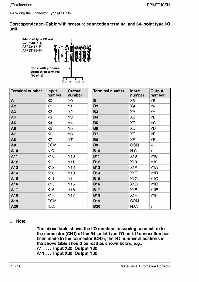
I/O Allocation FP3/FP10SH
4 − 30 Matsushita Automation Controls
4.4 Wiring the Connector Type I/O Units
Correspondence−Cable with pressure connection terminal and 64−point type I/Ounit
…
64−point type I/O unit(AFP33027−F,AFP33487−F,AFP33428−F)
Cable with pressureconnection terminal(40 pins)
Terminal number Inputnumber
Outputnumber
Terminal number Inputnumber
Outputnumber
A1 X0 Y0 B1 X8 Y8A2 X1 Y1 B2 X9 Y9A3 X2 Y2 B3 XA YAA4 X3 Y3 B4 XB YBA5 X4 Y4 B5 XC YCA6 X5 Y5 B6 XD YDA7 X6 Y6 B7 XE YEA8 X7 Y7 B8 XF YFA9 COM − B9 COM −A10 N.C. + B10 N.C. +A11 X10 Y10 B11 X18 Y18A12 X11 Y11 B12 X19 Y19A13 X12 Y12 B13 X1A Y1AA14 X13 Y13 B14 X1B Y1BA15 X14 Y14 B15 X1C Y1CA16 X15 Y15 B16 X1D Y1DA17 X16 Y16 B17 X1E Y1EA18 X17 Y17 B18 X1F Y1FA19 COM − B19 COM −A20 N.C. + B20 N.C. +
Note
The above table shows the I/O numbers assuming connection tothe connector (CN1) of the 64−point type I/O unit. If connection hasbeen made to the connector (CN2), the I/O number allocations inthe above table should be read as shown below, e.g.:A1 Input X20, Output Y20. . . .A11 Input X30, Output Y30. . .

I/O AllocationFP3/FP10SH
4 − 31Matsushita Automation Controls
4.4 Wiring the Connector Type I/O Units
4.4.4 Connecting with Connector for Wire−pressed Terminal Cable
This is a connector that allows lose wires to be connected without removing the wire’sinsulation.The pressure connection tool (AXY52000) is required to connect the loose wires.
Connector for wire−pressedterminal cable(20 pins)
Connector for wire−pressedterminal cable(40 pins)
Suitable wires (twisted wire)Size Cross section area Insulation thickness Rated current
AWG22 0.3 mm2dia 1 5 to dia 1 1 3 A
AWG24 0.2 mm2 dia. 1.5 to dia. 1.1 3 A
Contact puller pin for rewiringIf there is a wiring mistake or the wire is incorrectly pressure−connected, the contactpuller pin provided with the fitting can be used to remove the contact.
Press the housing against thepressure connection tool so that thecontact puller pin comes in contactwith this section.

I/O Allocation FP3/FP10SH
4 − 32 Matsushita Automation Controls
4.4 Wiring the Connector Type I/O Units
Assembly of connector for wire−pressed terminal cableThe wire end can be directly press−fitted without removing the wire‘s insulation, savinglabor.
Procedure:
1. Bend the contact back from the carrier, and set it inthe pressure connection tool.
2. Insert the wire without removing its insulation until itstops, and lightly grip the tool.
3. After press−fitting the wire, insert it into the housing.
4. When all wires has been inserted, fit the semi−coverinto place.
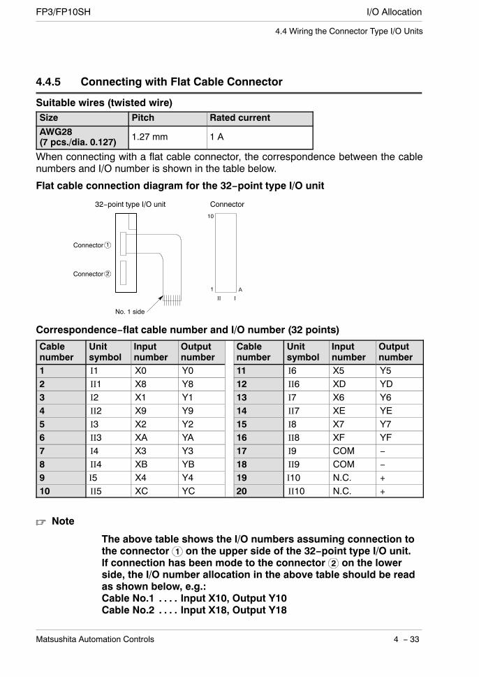
I/O AllocationFP3/FP10SH
4 − 33Matsushita Automation Controls
4.4 Wiring the Connector Type I/O Units
4.4.5 Connecting with Flat Cable Connector
Suitable wires (twisted wire)Size Pitch Rated current
AWG28(7 pcs./dia. 0.127) 1.27 mm 1 A
When connecting with a flat cable connector, the correspondence between the cablenumbers and I/O number is shown in the table below.
Flat cable connection diagram for the 32−point type I/O unit
32−point type I/O unit Connector
Connector
Connector
1
2
10
1 ΑII I
No. 1 side
Correspondence−flat cable number and I/O number (32 points)
Cablenumber
Unitsymbol
Inputnumber
Outputnumber
Cablenumber
Unitsymbol
Inputnumber
Outputnumber
1 I1 X0 Y0 11 I6 X5 Y52 II1 X8 Y8 12 II6 XD YD3 I2 X1 Y1 13 I7 X6 Y64 II2 X9 Y9 14 II7 XE YE5 I3 X2 Y2 15 I8 X7 Y76 II3 XA YA 16 II8 XF YF7 I4 X3 Y3 17 I9 COM −8 II4 XB YB 18 II9 COM −9 I5 X4 Y4 19 I10 N.C. +10 II5 XC YC 20 II10 N.C. +
Note
The above table shows the I/O numbers assuming connection tothe connector 1 on the upper side of the 32−point type I/O unit.If connection has been mode to the connector 2 on the lowerside, the I/O number allocation in the above table should be readas shown below, e.g.:Cable No.1 Input X10, Output Y10. . . .Cable No.2 Input X18, Output Y18. . . .
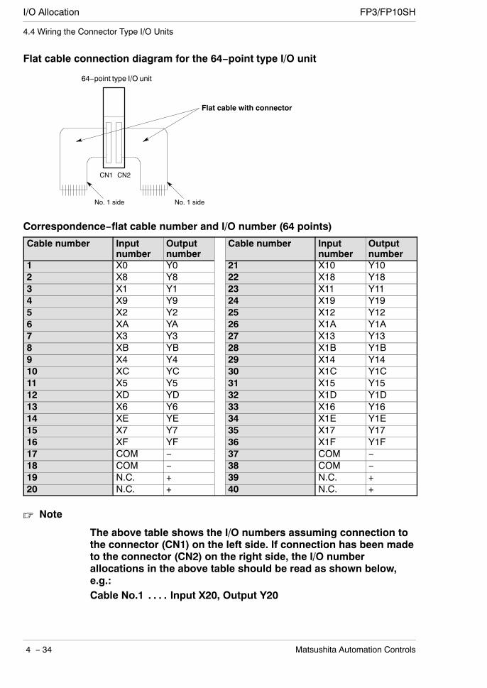
I/O Allocation FP3/FP10SH
4 − 34 Matsushita Automation Controls
4.4 Wiring the Connector Type I/O Units
Flat cable connection diagram for the 64−point type I/O unit
64−point type I/O unit
No. 1 sideNo. 1 side
CN1 CN2
Flat cable with connector
Correspondence−flat cable number and I/O number (64 points)
Cable number Inputnumber
Outputnumber
Cable number Inputnumber
Outputnumber
1 X0 Y0 21 X10 Y102 X8 Y8 22 X18 Y183 X1 Y1 23 X11 Y114 X9 Y9 24 X19 Y195 X2 Y2 25 X12 Y126 XA YA 26 X1A Y1A7 X3 Y3 27 X13 Y138 XB YB 28 X1B Y1B9 X4 Y4 29 X14 Y1410 XC YC 30 X1C Y1C11 X5 Y5 31 X15 Y1512 XD YD 32 X1D Y1D13 X6 Y6 33 X16 Y1614 XE YE 34 X1E Y1E15 X7 Y7 35 X17 Y1716 XF YF 36 X1F Y1F17 COM − 37 COM −18 COM − 38 COM −19 N.C. + 39 N.C. +20 N.C. + 40 N.C. +
Note
The above table shows the I/O numbers assuming connection tothe connector (CN1) on the left side. If connection has been madeto the connector (CN2) on the right side, the I/O numberallocations in the above table should be read as shown below,e.g.:Cable No.1 Input X20, Output Y20. . . .
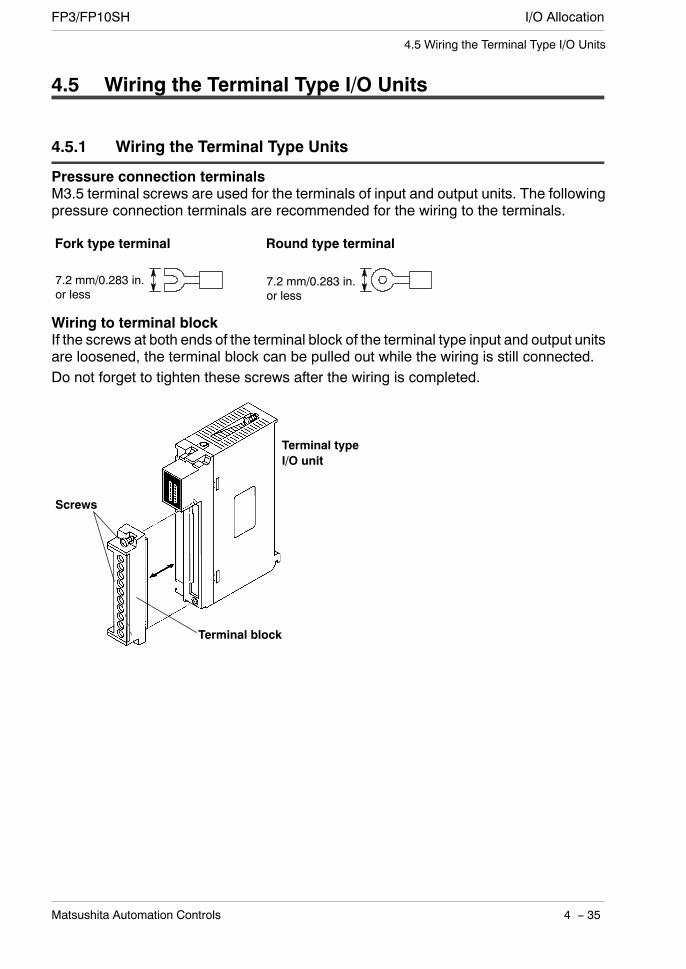
I/O AllocationFP3/FP10SH
4 − 35Matsushita Automation Controls
4.5 Wiring the Terminal Type I/O Units
4.5 Wiring the Terminal Type I/O Units
4.5.1 Wiring the Terminal Type Units
Pressure connection terminalsM3.5 terminal screws are used for the terminals of input and output units. The followingpressure connection terminals are recommended for the wiring to the terminals.
7.2 mm/0.283 in.or less
7.2 mm/0.283 in.or less
Fork type terminal Round type terminal
Wiring to terminal blockIf the screws at both ends of the terminal block of the terminal type input and output unitsare loosened, the terminal block can be pulled out while the wiring is still connected.Do not forget to tighten these screws after the wiring is completed.
Screws
Terminal block
Terminal typeI/O unit
I/O Allocation FP3/FP10SH
4 − 36 Matsushita Automation Controls
4.6 Safety Measures
4.6 Safety Measures
4.6.1 Safety Instructions
4.6.1.1 Precautions Regarding System Design
In certain applications, malfunction may occur for the following reasons:
Power ON timing differences between the FP3/FP10SH system and I/Oor motorized devices
An operation time lag when a momentary power failure occurs
Abnormality in the FP3/FP10SH, power supply circuit, or other devicesIn order to prevent a malfunction resulting in system shutdown choose the adequatessafety measures listed in the following:
4.6.1.2 Interlock Circuit
When a motor clockwise/counter-clockwise operation is controlled, provide an interlockcircuit that prevents clockwise and counter-clockwise signals from inputting into themotor at the same time.
4.6.1.3 Emergency Stop Circuit
Add an emergency stop circuit to controlled devices in order to prevent a systemshutdown or an irreparable accident when malfunction occurs.
4.6.1.4 Start Up Sequence
The FP3/FP10SH should be operated after all of the outside devices are energized. Tokeep this sequence, the following measures are recommended:
Set the mode selector from PROG. mode to RUN mode after power issupplied to all of the outside devices.
Program the FP3/FP10SH so as to disregard the inputs and outputs untilthe outside devices are energized.

I/O AllocationFP3/FP10SH
4 − 37Matsushita Automation Controls
4.6 Safety Measures
4.6.1.5 Alarm Function
When an alarm occurs, the FP3/FP10SH turns OFF the output and stops operation.Even while in this condition, take the appropriate safety precautions outside of theFP3/FP10SH to ensure no malfunction or damage is transmitted to anywhere else inthe system.
4.6.2 Momentary Power Failures
If a momentary power failure occurs, the resulting operations will differ depending onthe duration of the power failure.
Less than 10 ms: Operation continues.Between 10 ms and 20 ms: Depending on the conditions, the operation
may continue or may stop.More than 20 ms: The unit resets and the output turns OFF. When the
power returns, operation starts from its initial conditions.
4.6.3 Alarm Output
The alarm output goes ON when the watchdog timer (* section 4.6.3.1) is activated bya program error (eg., infinite loop) or an error in the hardware itself.The alarm output terminal has two relay contacts, N.O. (normally open) and N.C.(normally closed) on the power supply unit, which can be used as external alarmsignals.
Lamp foralarm signal
Power supply
L
Power supply unit
Note
Be aware that the alarm output for power supply unit that areinstalled to the expansion backplanes will not work.

I/O Allocation FP3/FP10SH
4 − 38 Matsushita Automation Controls
4.6 Safety Measures
4.6.3.1 Watchdog Timer
The watchdog timer is a program error and hardware error detection timer. It goes ONwhen the scan time exceeds 640 ms.When the watchdog timer is activated, at the same time the ALARM LED lights, theALARM contacts on the power supply unit go ON, all outputs to the output units areturned OFF and the unit is put in halted state. (The system is in a non-processing statethat includes communications with programming tools as well.)
Chapter 5
Procedure Until Operation
5.1 Before Turning ON the Power 5 − 3. . . . . . . . . . . . . .
5.1.1 Check Items 5 − 3. . . . . . . . . . . . . . . . . . . . .
5.1.2 Procedure Up To Trial Operation 5 − 4. . . .
5.2 Programming with NPST−GR 5 − 5. . . . . . . . . . . . . .
5.2.1 Preparations 5 − 5. . . . . . . . . . . . . . . . . . . . .
5.2.2 Configuring NPST−GR 5 − 6. . . . . . . . . . . .
5.3 Programming with an FP Programmer II 5 − 9. . . . .
5.3.1 Preparations 5 − 9. . . . . . . . . . . . . . . . . . . . .
5.4 Operation of FP3 5 − 11. . . . . . . . . . . . . . . . . . . . . . . .
5.4.1 RAM and ROM Operations 5 − 11. . . . . . .
5.4.2 Holding the Data During PowerFailure 5 − 12. . . . . . . . . . . . . . . . . . . . . . . . .
5.4.3 Precautions for ROM Operation 5 − 13. . .
5.4.4 Writing to ROM 5 − 15. . . . . . . . . . . . . . . . . .
5.5 Operation of FP10SH 5 − 19. . . . . . . . . . . . . . . . . . . .
5.5.1 RAM, ROM and IC Memory CardOperations 5 − 19. . . . . . . . . . . . . . . . . . . . .
5.5.2 Holding the Data During PowerFailure 5 − 21. . . . . . . . . . . . . . . . . . . . . . . . .
5.6 How To Use a ROM Operation Board(for FP10SH only) 5 − 22. . . . . . . . . . . . . . . . . . . . . . .
5.6.1 Overview of FP10SH ROM OperationBoard 5 − 22. . . . . . . . . . . . . . . . . . . . . . . . . .
5.6.2 Function of ROM Operation Board 5 − 23.
5.6.3 Precautions for ROM Operation 5 − 25. . .
5.6.4 Transfer Data from RAM to FROM 5 − 27.
5.6.5 Writing to ROM 5 − 28. . . . . . . . . . . . . . . . . .
next page

I/O Allocation FP3/FP10SH
5 − 2 Matsushita Automation Controls
5.7 How To Use IC Card Board(for FP10SH only) 5 − 32. . . . . . . . . . . . . . . . . . . . . . .
5.7.1 Overview of FP10SH IC Card Board 5 − 32
5.7.2 Function of IC Card Board 5 − 33. . . . . . . .
5.7.3 Precautions for IC Memory CardOperation 5 − 36. . . . . . . . . . . . . . . . . . . . . .
I/O AllocationFP3/FP10SH
5 − 3Matsushita Automation Controls
5.1 Before Turning ON the Power
5.1 Before Turning ON the Power
5.1.1 Check Items
After wiring, be sure to check the items below before turning ON the power supply tothe FP3/FP10SH system.
Item Description
Unit mountingstatus
−Does the unit type match the device list during the design stage?−Are the unit mounting screws properly tightened?−Is the unit dust protected label detached?
Power supply unit −Is power supply voltage supplied correctly?−For power supply units AFP3631 and AFP3638, are the voltageswitch terminals shorted together for 100 to 120 V AC operationand open for 200 to 240 V AC operation?
−Are the terminal block mounting screws properly tightened?−Is the wire size correct?
Input/Output units −Does the wiring of connector and terminal match?−Is the operating voltage of I/O correct?−Are the terminal block mounting screws properly tightened?−Is the wire size correct?
Expansion cable −Are the expansion cables properly connected?
Board numbersetting
−Are they set so that numbers are not identical?(If expansion backplane are used, the numbers for the boardnumber set switch must be set.)
Setting of CPU −Is the mode selector set to the PROG. mode?−Is the backup battery connector firmly connected?−Has the DIP switch of CPU been set correctly?
ROM mountingstatus
−Has the ROM been mounted in the correct direction?−Has the ROM been securely installed? Are the lead feet firmlysecured and not likely to come loose?
−For the FP3, does the ROM type match the position of device(ROM type) selector?
I/O Allocation FP3/FP10SH
5 − 4 Matsushita Automation Controls
5.1 Before Turning ON the Power
5.1.2 Procedure Up To Trial Operation
After installing and wiring, perform the trial operation by following procedure.
Procedure:
1. Before turning ON the power, check the itemsdescribed on the previous page
2. Turn ON the power
3. Check that the power supply unit’s POWER LED andCPU’s PROG. LED are ON
4. Enter the programWhen using a programming tool, perform the operation “Clear Program”before inputting. Enter the program using the programming tool. Use theproramming tool’s “total check function” to check for syntax errors.
5. Check output wiringUse the forced output function to check the output wiring.
6. Check input wiringCheck the input wiring by watching the ON/OFF status of the input LEDs ofinput unit or by using the monitoring function of the programming tool.
7. Switch the mode selector from PROG. to RUN mode
8. If the RUN LED turns ON, check the operation of theprogram
9. Edit the program (debug) if necessaryIf there is an error in the operation, check the program using the monitoringfunction of the programming tool. And then correct the program.
10. Save the edited programWe highly recommend to save the created program onto a floppy disk.Printing out is also possible.The program can also be saved on ROM for FP3 and on an IC memorycard or ROM for FP10SH.
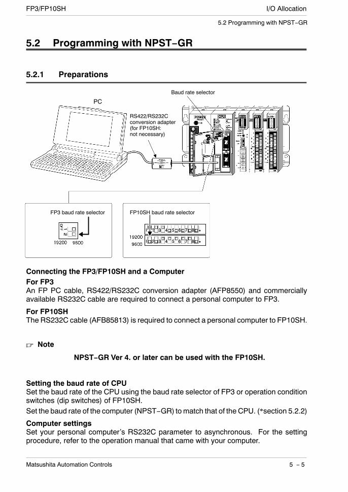
I/O AllocationFP3/FP10SH
5 − 5Matsushita Automation Controls
5.2 Programming with NPST−GR
5.2 Programming with NPST−GR
5.2.1 Preparations
RS422/RS232Cconversion adapter(for FP10SH:not necessary)
Baud rate selector
FP3 baud rate selector FP10SH baud rate selector
PC
Connecting the FP3/FP10SH and a ComputerFor FP3An FP PC cable, RS422/RS232C conversion adapter (AFP8550) and commerciallyavailable RS232C cable are required to connect a personal computer to FP3.
For FP10SHThe RS232C cable (AFB85813) is required to connect a personal computer to FP10SH.
Note
NPST−GR Ver 4. or later can be used with the FP10SH.
Setting the baud rate of CPUSet the baud rate of the CPU using the baud rate selector of FP3 or operation conditionswitches (dip switches) of FP10SH.Set the baud rate of the computer (NPST−GR) tomatch that of the CPU. (*section 5.2.2)
Computer settingsSet your personal computer’s RS232C parameter to asynchronous. For the settingprocedure, refer to the operation manual that came with your computer.
I/O Allocation FP3/FP10SH
5 − 6 Matsushita Automation Controls
5.2 Programming with NPST−GR
5.2.2 Configuring NPST−GR
Depending on the PLC type and communication speed (baud rate), it is necessary toset the basic configuration for NPST−GR. Be sure to set these items (parameters)before beginning programming.
SCREEN MODE[MONO/COLOR]Select either black−and−white (monochrome) or color for the display of the NPST−GRscreen mode.
PLC TYPESelect the PLC (programmable controller) type that is being used.
Communication formatThe baud rate setting must match that of the CPU that is connected. (* section 5.2.1)
LOGGED DRIVE/DIRECTORYSelect the disk drive and directory from which the program and file are to be read.
NOTE DISPLAYSelect whether or not to display the title and the title is to be added to the filename whendisplaying the filename.
PROGRAMMING MODE[Ladder symbol mode, Boolean ladder mode and Boolean non−ladder mode]Select the inputting method for creating and editing the program.
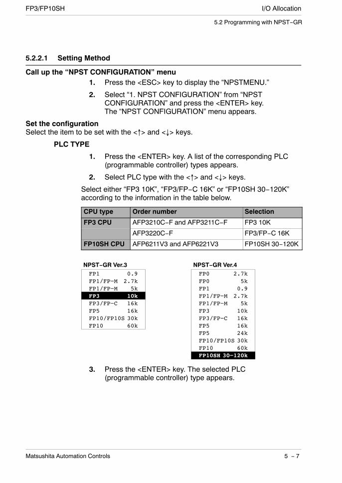
I/O AllocationFP3/FP10SH
5 − 7Matsushita Automation Controls
5.2 Programming with NPST−GR
5.2.2.1 Setting Method
Call up the “NPST CONFIGURATION” menu1. Press the <ESC> key to display the “NPSTMENU.”
2. Select “1. NPST CONFIGURATION” from “NPSTCONFIGURATION” and press the <ENTER> key.The “NPST CONFIGURATION” menu appears.
Set the configurationSelect the item to be set with the <↑> and <↓> keys.
PLC TYPE
1. Press the <ENTER> key. A list of the corresponding PLC(programmable controller) types appears.
2. Select PLC type with the <↑> and <↓> keys.Select either “FP3 10K”, “FP3/FP−C 16K” or “FP10SH 30−120K”according to the information in the table below.
CPU type Order number Selection
FP3 CPU AFP3210C−F and AFP3211C−F FP3 10K
AFP3220C−F FP3/FP−C 16K
FP10SH CPU AFP6211V3 and AFP6221V3 FP10SH 30−120K
FP1 0.9FP1/FP−M 2.7kFP1/FP−M 5kFP3 10kFP3/FP−C 16kFP5 16kFP10/FP10S 30kFP10 60k
NPST−GR Ver.3FP0 2.7kFP0 5kFP1 0.9FP1/FP−M 2.7kFP1/FP−M 5kFP3 10kFP3/FP−C 16kFP5 16kFP5 24kFP10/FP10S 30kFP10 60kFP10SH 30−120k
NPST−GR Ver.4
3. Press the <ENTER> key. The selected PLC(programmable controller) type appears.
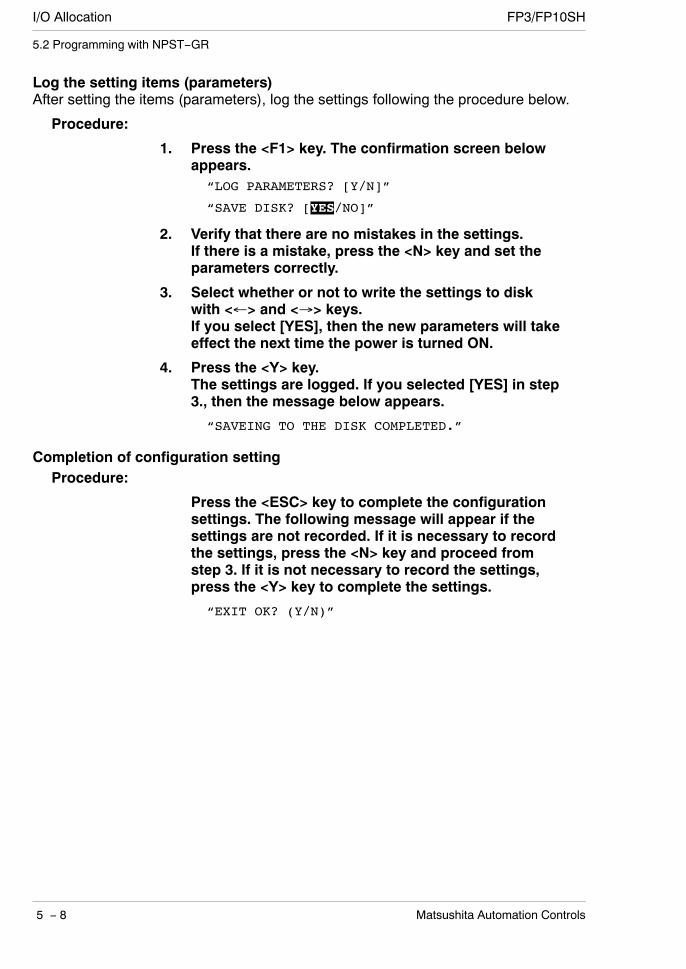
I/O Allocation FP3/FP10SH
5 − 8 Matsushita Automation Controls
5.2 Programming with NPST−GR
Log the setting items (parameters)After setting the items (parameters), log the settings following the procedure below.
Procedure:
1. Press the <F1> key. The confirmation screen belowappears.“LOG PARAMETERS? [Y/N]”
“SAVE DISK? [YES/NO]”
2. Verify that there are no mistakes in the settings.If there is a mistake, press the <N> key and set theparameters correctly.
3. Select whether or not to write the settings to diskwith <←> and <→> keys.If you select [YES], then the new parameters will takeeffect the next time the power is turned ON.
4. Press the <Y> key.The settings are logged. If you selected [YES] in step3., then the message below appears.
“SAVEING TO THE DISK COMPLETED.”
Completion of configuration settingProcedure:
Press the <ESC> key to complete the configurationsettings. The following message will appear if thesettings are not recorded. If it is necessary to recordthe settings, press the <N> key and proceed fromstep 3. If it is not necessary to record the settings,press the <Y> key to complete the settings.
“EXIT OK? (Y/N)”

I/O AllocationFP3/FP10SH
5 − 9Matsushita Automation Controls
5.3 Programming with an FP Programmer II
5.3 Programming with an FP Programmer II
5.3.1 Preparations
FP programmer IIAFP1114V2
FP peripheral cableAFP5520(50 cm/19.69 in.)AFP5523(3 m/9.84 ft.)
Baud rate selector
FP3 baud rate selector
Connecting the FP3 and an FP programmer IIAn FP peripheral cable is required to connect an FP3 to an FP programmer II.
− FP peripheral cable :50 cm/19.69 in (AFP5520)3 m/9.84 ft. (AFP5523)
Setting the baud rate of the CPUSet the baud rate of CPU using the baud rate selector.When using the FP programmer II, a baud rate of either 9,600 bps or 19,200 bps canbe selected.
Storage location of programsThe programs input with the FP programmer II are stored one after another in the FP3’sbuilt-in memory (RAM).
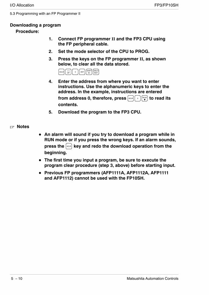
I/O Allocation FP3/FP10SH
5 − 10 Matsushita Automation Controls
5.3 Programming with an FP Programmer II
Downloading a programProcedure:
1. Connect FP programmer II and the FP3 CPU usingthe FP peripheral cable.
2. Set the mode selector of the CPU to PROG.
3. Press the keys on the FP programmer II, as shownbelow, to clear all the data stored.
0 ENT SCSHIFT
INST(DELT)
ACLR OP(−)
4. Enter the address from where you want to enterinstructions. Use the alphanumeric keys to enter theaddress. In the example, instructions are enteredfrom address 0, therefore, press 0ACLR READ to read itscontents.
5. Download the program to the FP3 CPU.
Notes
An alarm will sound if you try to download a program while inRUN mode or if you press the wrong keys. If an alarm sounds,press the ACLR key and redo the download operation from thebeginning.
The first time you input a program, be sure to execute theprogram clear procedure (step 3, above) before starting input.
Previous FP programmers (AFP1111A, AFP1112A, AFP1111and AFP1112) cannot be used with the FP10SH.
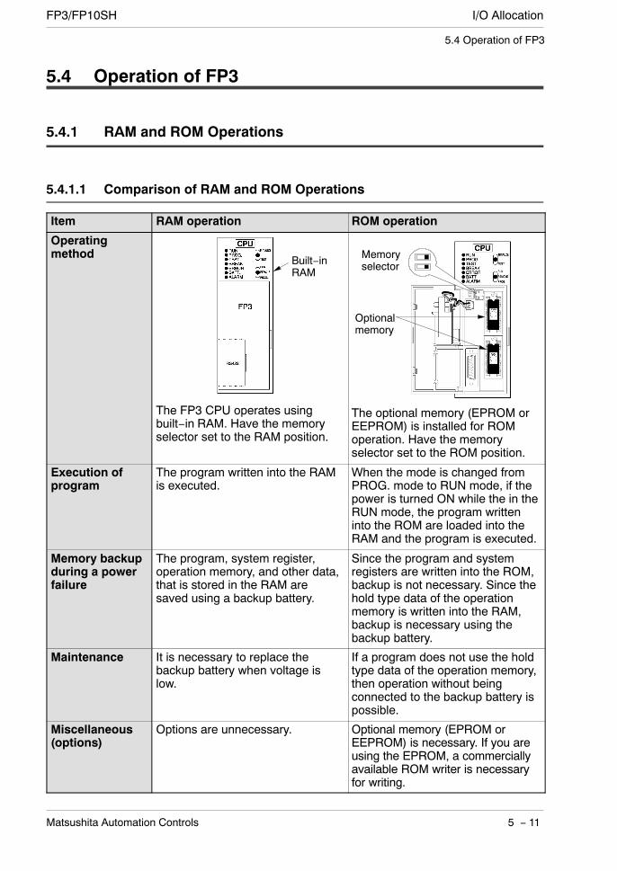
I/O AllocationFP3/FP10SH
5 − 11Matsushita Automation Controls
5.4 Operation of FP3
5.4 Operation of FP3
5.4.1 RAM and ROM Operations
5.4.1.1 Comparison of RAM and ROM Operations
Item RAM operation ROM operation
Operatingmethod
The FP3 CPU operates usingbuilt−in RAM. Have the memoryselector set to the RAM position.
Built−inRAM
The optional memory (EPROM orEEPROM) is installed for ROMoperation. Have the memoryselector set to the ROM position.
Memoryselector
Optionalmemory
Execution ofprogram
The program written into the RAMis executed.
When the mode is changed fromPROG. mode to RUN mode, if thepower is turned ON while the in theRUN mode, the program writteninto the ROM are loaded into theRAM and the program is executed.
Memory backupduring a powerfailure
The program, system register,operation memory, and other data,that is stored in the RAM aresaved using a backup battery.
Since the program and systemregisters are written into the ROM,backup is not necessary. Since thehold type data of the operationmemory is written into the RAM,backup is necessary using thebackup battery.
Maintenance It is necessary to replace thebackup battery when voltage islow.
If a program does not use the holdtype data of the operation memory,then operation without beingconnected to the backup battery ispossible.
Miscellaneous(options)
Options are unnecessary. Optional memory (EPROM orEEPROM) is necessary. If you areusing the EPROM, a commerciallyavailable ROM writer is necessaryfor writing.
I/O Allocation FP3/FP10SH
5 − 12 Matsushita Automation Controls
5.4 Operation of FP3
5.4.2 Holding the Data During Power Failure
5.4.2.1 Backup of Operation Memory
The internal relay, data registers and other hold type data are backed up by the battery.When performing ROM operation with the internal relay, data registers, and other suchdata set to non− hold type data, you can perform operation without being connectedto a backup battery.
5.4.2.2 Setting the Battery Error Warnings
With the exception of FP3 CPU version 4.4 or greater, if the CPU is set with the batteryerror warning disabled, the ERROR LED does not light even if operating while not beingconnected to a backup battery. Set the battery error warning according to the followingprocedure:
Procedure:For NPST−GR software
1. Press the <ESC> key to display the [NPST MENU].In the [NPST MENU] screen, select the [SYSTEMREGISTER] option from the [PLC CONFIGURATION]and press <ENTER> key.
2. In the [PLC CONFIGURATION] screen, press the <F8>key and select the [ACT ON ERROR] option. Then setthe [BATTERY ERROR] to [DISABLE].
3. Press the <F1> key to save the setting contents.4. Press the <ESC> key and then the <Y> key to return
to the original screen.For FP Programmer II
1. Use the following key sequence for the systemregister
(−)OP 5 0 ENT
2. To read contents of system register 4 , press thefollowing keys
READΒ4
3. To disable the battery error warning, press thefollowing keys.ACLR 1 WRT
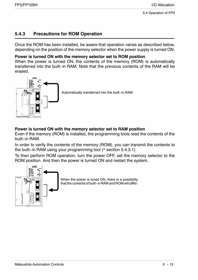
I/O AllocationFP3/FP10SH
5 − 13Matsushita Automation Controls
5.4 Operation of FP3
5.4.3 Precautions for ROM Operation
Once the ROM has been installed, be aware that operation varies as described below,depending on the position of the memory selector when the power supply is turned ON.
Power is turned ON with the memory selector set to ROM positionWhen the power is turned ON, the contents of the memory (ROM) is automaticallytransferred into the built−in RAM. Note that the previous contents of the RAM will beerased.
Automatically transferred into the built−in RAM
Power is turned ON with the memory selector set to RAM positionEven if the memory (ROM) is installed, the programming tools read the contents of thebuilt−in RAM.In order to verify the contents of the memory (ROM), you can transmit the contents tothe built−in RAM using your programming tool (* section 5.4.3.1).To then perform ROM operation, turn the power OFF, set the memory selector to theROM position. And then the power is turned ON and restart the system.
When the power is tuned ON, there is a possibilitythat the contents of built−inRAMandROMwill differ.
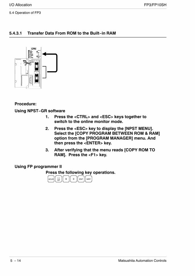
I/O Allocation FP3/FP10SH
5 − 14 Matsushita Automation Controls
5.4 Operation of FP3
5.4.3.1 Transfer Data From ROM to the Built−in RAM
Procedure:
Using NPST−GR software1. Press the <CTRL> and <ESC> keys together to
switch to the online monitor mode.
2. Press the <ESC> key to display the [NPST MENU].Select the [COPY PROGRAM BETWEEN ROM & RAM]option from the [PROGRAM MANAGER] menu. Andthen press the <ENTER> key.
3. After verifying that the menu reads [COPY ROM TORAM]. Press the <F1> key.
Using FP programmer IIPress the following key operations.
(−)OP 9 0 ENTACLR WRT
I/O AllocationFP3/FP10SH
5 − 15Matsushita Automation Controls
5.4 Operation of FP3
5.4.4 Writing to ROM
5.4.4.1 Using a Commercially Available ROM Writer Via EEPROM
Procedure:
1. Turn OFF the power and attach the master memory(EEPROM) to the CPU.Set the device (ROM type) selector to the EEPROMposition.
2. Verify that the mode selector is set to PROG. modeand then turn ON the power.
3. When using the NPST−GR or FP programmer II,transfer the contents of the built−in RAM to themaster memory (EEPROM). (* refer to the next page)
4. Turn OFF the power, and detach the programmedmaster memory (EEPROM) from the CPU and attach itin the commercially available ROM writer.
5. Transfer the contents of master memory (EEPROM)to the ROM writer
Transfer
next page
I/O Allocation FP3/FP10SH
5 − 16 Matsushita Automation Controls
5.4 Operation of FP3
6. Remove the master memory (EEPROM) and installthe memory (EPROM) and write the contents of theROM writer to the memory (EPROM).
Write
Note
Refer to the manual of commercially available ROM writer foroperation procedure and setting of ROM.
Transfer data from the built−in RAM to master memory (EEPROM)Procedure:
Using NPST−GR software1. Press the <CTRL> and <ESC> keys together to
switch to the online monitor mode.
2. Press the <ESC> key to display the [NPST MENU].Select the [COPY PROGRAM BETWEEN ROM & RAM]option from the [PROGRAM MANAGER] menu. Andthen press the <ENTER> key.
3. Press the <F2> key to switch to [COPY RAM TOROM].
4. Press the <F1> key. The contents of the built−in RAMare transfered to EEPROM.
Using the FP programmer IIPress the following key operations.
(−)OP 9 9 ENTACLR WRT
Note
If you want to write the contents of built−in RAM of the FP3 to themaster memory (EEPROM), be sure to verify that the memoryselector is set to the RAM position before turning ON the power.
I/O AllocationFP3/FP10SH
5 − 17Matsushita Automation Controls
5.4 Operation of FP3
5.4.4.2 Using NPST−GR and a Commercially Available ROM Writer
Procedure:
1. In the NPST−GR at the computer, select the [LOADTO/FROM ROM WRITER] option to transfer the pro-gram to the commercially available ROM writer.
2. Attach the memory (EPROM) in the commerciallyavailable ROM witer.Write the data to the memory (EPROM) with thecommercially available ROM writer.
Note
Refer to the manual for the commercially available ROM writer forthe proper settings.
Transfer program from the computer with NPST−GR to the ROM writerProcedure:
1. In the [NPST CONFIGURATION] menu, press the<SHIFT> and <F6> keys together to display the [ROMCONFIG].
<ROM CONFIG> window
TRANS RATE (bps) [ 9600 Σ 4800 Σ 2400 Σ 1200 Σ 600 Σ 300 ]
DATA LENGTH [ 8 Σ 7 ]
PARITY CHECK [ NO Σ EV Σ OD ]
STOP BIT [ 1 Σ 2 ]
next page

I/O Allocation FP3/FP10SH
5 − 18 Matsushita Automation Controls
5.4 Operation of FP3
2. Set the transmission rate and communication formatthat matches that for the ROM writer with, and press<F1> key to save the settings.
3. Press the <ESC> key, and select [PROGRAMMANAGER] from the [NPST MENU] then select the[LOAD TO/FROM ROM WRITER] option. Press the<ENTER> key.
[LOAD TO/FROM ROM WRITER]
READ WRITE VRFY
INTEL HEX MOTOROLA [S]
SERIAL PORT CENTRNICS PORT FILE
NO PASSWORD WITH PASSWORD
F1 : EXECUTE.
4. Specify the transmission format and connectionmethod appropriate for the ROM writer and thenselect [WRITE]. Press the <F1> key. The program istransfered to the ROM writer.
I/O AllocationFP3/FP10SH
5 − 19Matsushita Automation Controls
5.5 Operation of FP10SH
5.5 Operation of FP10SH
5.5.1 RAM, ROM and IC Memory Card Operations
5.5.1.1 Comparison of RAM, ROM and IC Memory Card Operation
Item RAM operation ROM operation IC memory cardoperation
Operatingmethod
Built−inRAM ROM operation board
or IC card board
This operates based onbuilt−in RAM of CPU. Setthe program memoryswitch (SW5) to OFF(* section 2.5.1.4).
The optional ROMoperating board isinstalled for ROMoperation. Set the programmemory switch (SW5) toON. (* section 2.5.1.4).
The optional IC memorycard and IC card boardare installed for ICmemory card operation.Set the program memoryswitch (SW5) to ON.(* section 2.5.1.4).
Execution ofprogram
The program written intothe RAM is executed.
When the power is turnedON, the program writteninto ROM are transferredinto the RAM and theprogram is executed.
Turning the power ON willtransferred the program(file named AUTOEXEC.SPG) of the IC memorycard into the RAM andexecute the program.Using the F14(PGRD)/P14 (PPGRD)instructions, it is possibleto read out the program(with an arbitrary filename) stored in the ICmemory card.
next page
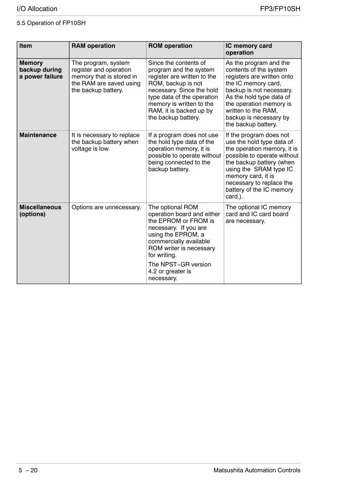
I/O Allocation FP3/FP10SH
5 − 20 Matsushita Automation Controls
5.5 Operation of FP10SH
Item RAM operation ROM operation IC memory cardoperation
Memorybackup duringa power failure
The program, systemregister and operationmemory that is stored inthe RAM are saved usingthe backup battery.
Since the contents ofprogram and the systemregister are written to theROM, backup is notnecessary. Since the holdtype data of the operationmemory is written to theRAM, it is backed up bythe backup battery.
As the program and thecontents of the systemregisters are written ontothe IC memory card,backup is not necessary.As the hold type data ofthe operation memory iswritten to the RAM,backup is necessary bythe backup battery.
Maintenance It is necessary to replacethe backup battery whenvoltage is low.
If a program does not usethe hold type data of theoperation memory, it ispossible to operate withoutbeing connected to thebackup battery.
If the program does notuse the hold type data ofthe operation memory, it ispossible to operate withoutthe backup battery (whenusing the SRAM type ICmemory card, it isnecessary to replace thebattery of the IC memorycard.).
Miscellaneous(options)
Options are unnecessary. The optional ROMoperation board and eitherthe EPROM or FROM isnecessary. If you areusing the EPROM, acommercially availableROM writer is necessaryfor writing.
The NPST−GR version4.2 or greater isnecessary.
The optional IC memorycard and IC card boardare necessary.
I/O AllocationFP3/FP10SH
5 − 21Matsushita Automation Controls
5.5 Operation of FP10SH
5.5.2 Holding the Data During Power Failure
5.5.2.1 Backup of Operation Memory
The internal relay, data registers and other hold type data are backed up by the battery.When performing ROM operation or IC memory card operation with the internal relay,data registers, and other such data set to non− hold type data, you can performoperation without being connected to a backup battery.
5.5.2.2 Setting the Battery Error Warnings
If the FP10SH CPU is set with the battery error warning disabled using system register4, the ERROR LED does not light even if operating while not being connected to abattery.Set the battery error warning according to the following procedure:
Procedure:
For NPST−GR software
1. Press the <ESC> key to display the [NPST MENU].In the [NPST MENU] screen, select the [SYSTEMREGISTER] option from the [PLC CONFIGURATION]and press the <ENTER> key.
2. In the [PLC CONFIGURATION] menu, press the <F8>key and select the [ACT ON ERROR] option. Then setthe [BATTERY ERROR] to [DISABLE].
3. Press the <F1> key to save the setting contents.
4. Press the <ESC> key and then the <Y> key to returnto the original screen.
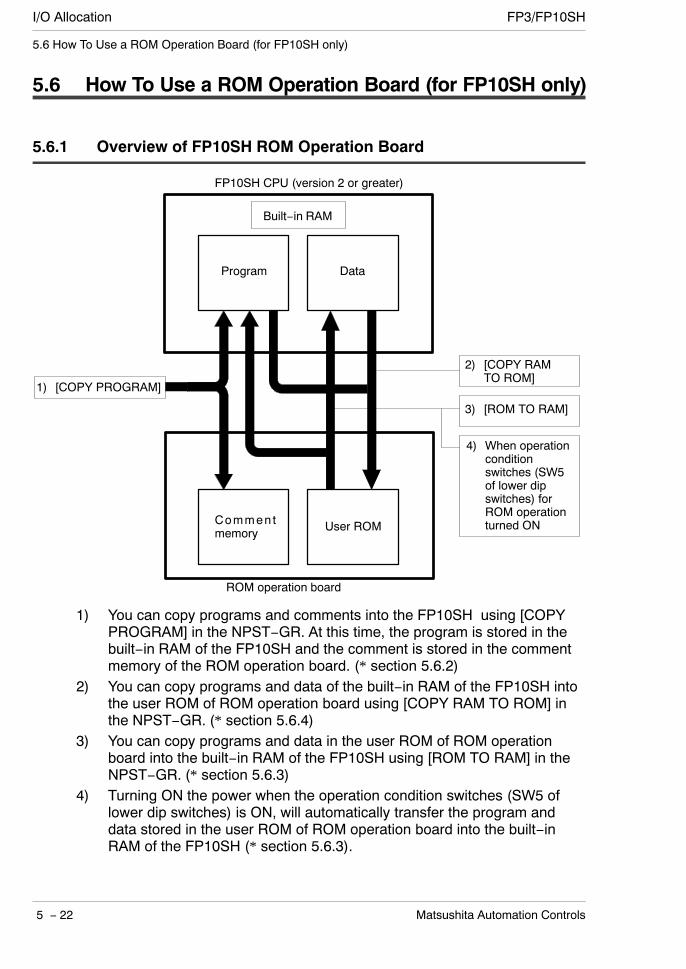
I/O Allocation FP3/FP10SH
5 − 22 Matsushita Automation Controls
5.6 How To Use a ROM Operation Board (for FP10SH only)
5.6 How To Use a ROM Operation Board (for FP10SH only)
5.6.1 Overview of FP10SH ROM Operation Board
3) [ROM TO RAM]
FP10SH CPU (version 2 or greater)
Built−in RAM
Program Data
1) [COPY PROGRAM]
Commentmemory User ROM
ROM operation board
2) [COPY RAMTO ROM]
4) When operationconditionswitches (SW5of lower dipswitches) forROM operationturned ON
1) You can copy programs and comments into the FP10SH using [COPYPROGRAM] in the NPST−GR. At this time, the program is stored in thebuilt−in RAM of the FP10SH and the comment is stored in the commentmemory of the ROM operation board. (* section 5.6.2)
2) You can copy programs and data of the built−in RAM of the FP10SH intothe user ROM of ROM operation board using [COPY RAM TO ROM] inthe NPST−GR. (* section 5.6.4)
3) You can copy programs and data in the user ROM of ROM operationboard into the built−in RAM of the FP10SH using [ROM TO RAM] in theNPST−GR. (* section 5.6.3)
4) Turning ON the power when the operation condition switches (SW5 oflower dip switches) is ON, will automatically transfer the program anddata stored in the user ROM of ROM operation board into the built−inRAM of the FP10SH (* section 5.6.3).
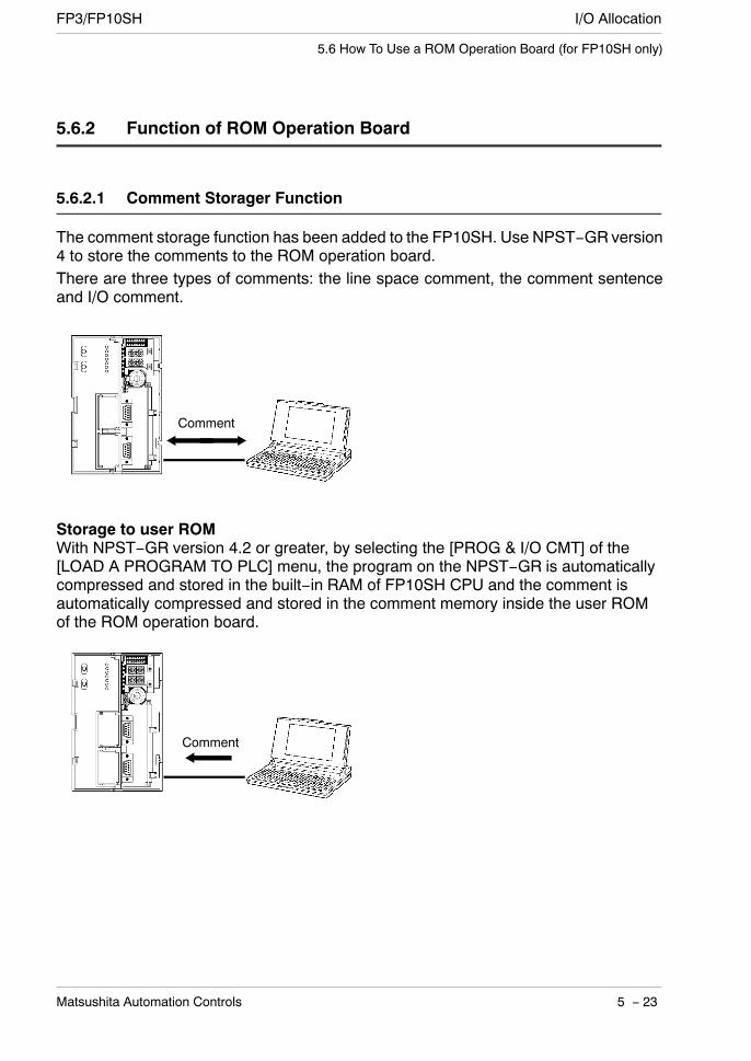
I/O AllocationFP3/FP10SH
5 − 23Matsushita Automation Controls
5.6 How To Use a ROM Operation Board (for FP10SH only)
5.6.2 Function of ROM Operation Board
5.6.2.1 Comment Storager Function
The comment storage function has been added to the FP10SH. Use NPST−GRversion4 to store the comments to the ROM operation board.There are three types of comments: the line space comment, the comment sentenceand I/O comment.
Comment
Storage to user ROMWith NPST−GR version 4.2 or greater, by selecting the [PROG & I/O CMT] of the[LOAD A PROGRAM TO PLC] menu, the program on the NPST−GR is automaticallycompressed and stored in the built−in RAM of FP10SH CPU and the comment isautomatically compressed and stored in the comment memory inside the user ROMof the ROM operation board.
Comment
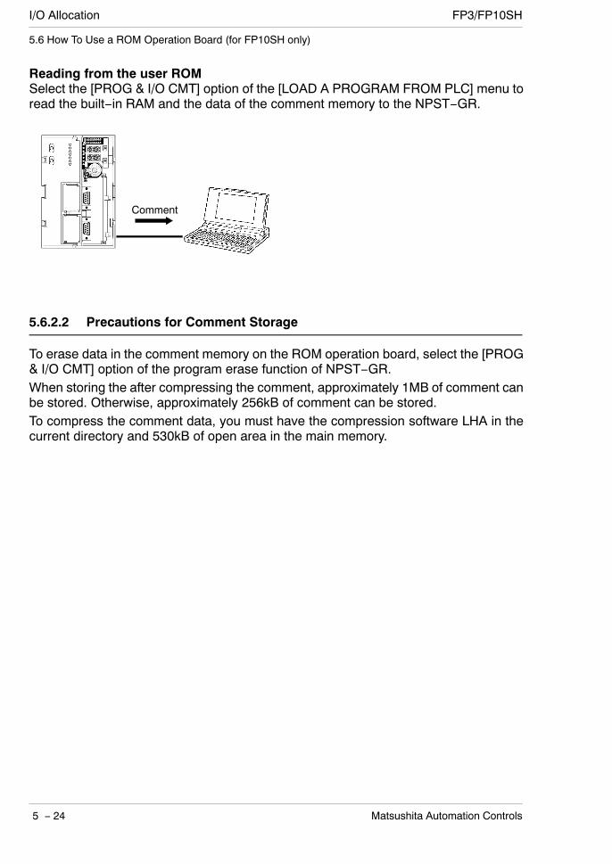
I/O Allocation FP3/FP10SH
5 − 24 Matsushita Automation Controls
5.6 How To Use a ROM Operation Board (for FP10SH only)
Reading from the user ROMSelect the [PROG & I/O CMT] option of the [LOAD A PROGRAM FROM PLC] menu toread the built−in RAM and the data of the comment memory to the NPST−GR.
Comment
5.6.2.2 Precautions for Comment Storage
To erase data in the comment memory on the ROM operation board, select the [PROG& I/O CMT] option of the program erase function of NPST−GR.When storing the after compressing the comment, approximately 1MB of comment canbe stored. Otherwise, approximately 256kB of comment can be stored.To compress the comment data, you must have the compression software LHA in thecurrent directory and 530kB of open area in the main memory.
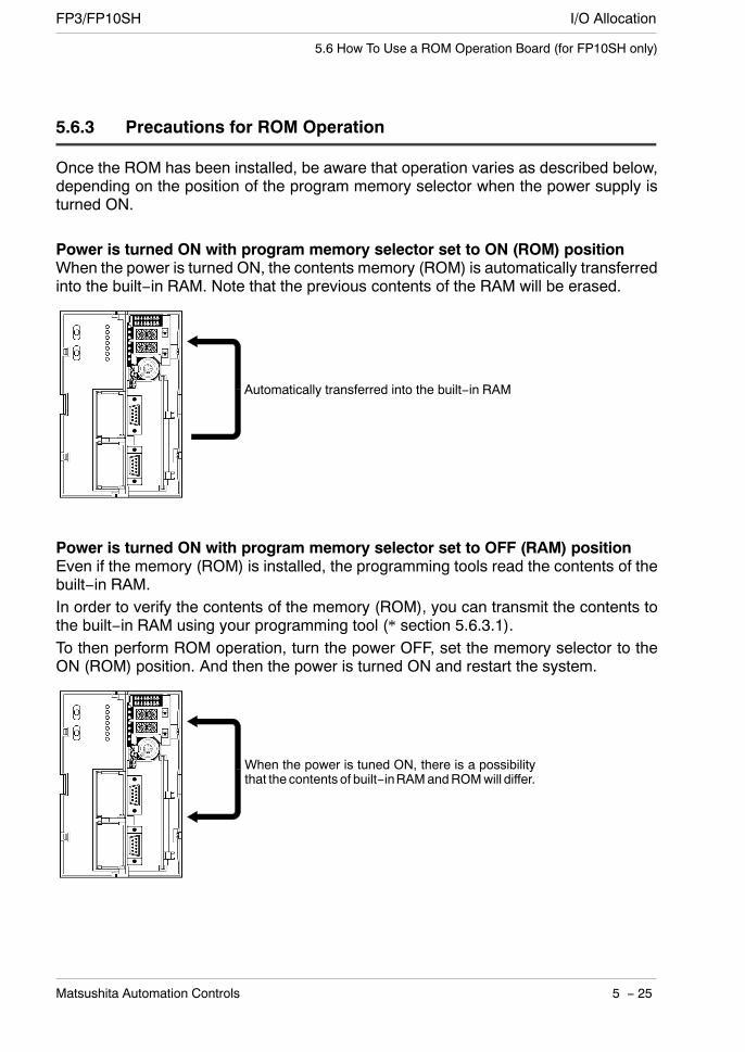
I/O AllocationFP3/FP10SH
5 − 25Matsushita Automation Controls
5.6 How To Use a ROM Operation Board (for FP10SH only)
5.6.3 Precautions for ROM Operation
Once the ROM has been installed, be aware that operation varies as described below,depending on the position of the program memory selector when the power supply isturned ON.
Power is turned ON with program memory selector set to ON (ROM) positionWhen the power is turned ON, the contents memory (ROM) is automatically transferredinto the built−in RAM. Note that the previous contents of the RAM will be erased.
Automatically transferred into the built−in RAM
Power is turned ON with program memory selector set to OFF (RAM) positionEven if the memory (ROM) is installed, the programming tools read the contents of thebuilt−in RAM.In order to verify the contents of the memory (ROM), you can transmit the contents tothe built−in RAM using your programming tool (* section 5.6.3.1).To then perform ROM operation, turn the power OFF, set the memory selector to theON (ROM) position. And then the power is turned ON and restart the system.
When the power is tuned ON, there is a possibilitythat the contents of built−inRAMandROMwill differ.
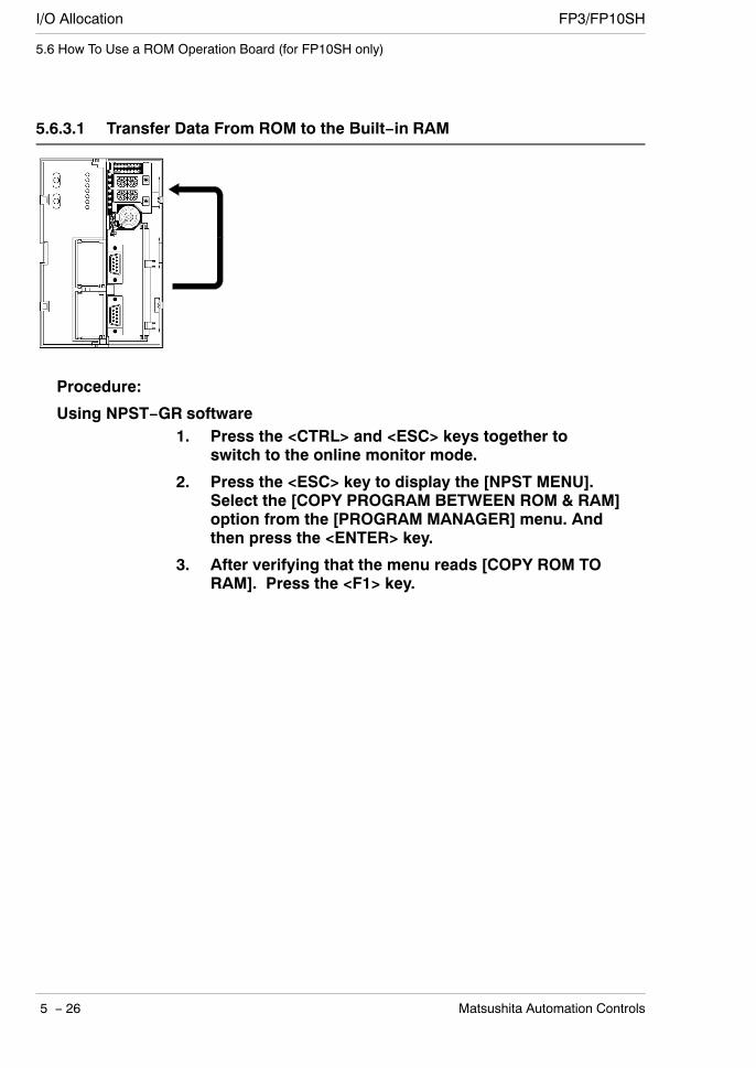
I/O Allocation FP3/FP10SH
5 − 26 Matsushita Automation Controls
5.6 How To Use a ROM Operation Board (for FP10SH only)
5.6.3.1 Transfer Data From ROM to the Built−in RAM
Procedure:
Using NPST−GR software1. Press the <CTRL> and <ESC> keys together to
switch to the online monitor mode.
2. Press the <ESC> key to display the [NPST MENU].Select the [COPY PROGRAM BETWEEN ROM & RAM]option from the [PROGRAM MANAGER] menu. Andthen press the <ENTER> key.
3. After verifying that the menu reads [COPY ROM TORAM]. Press the <F1> key.
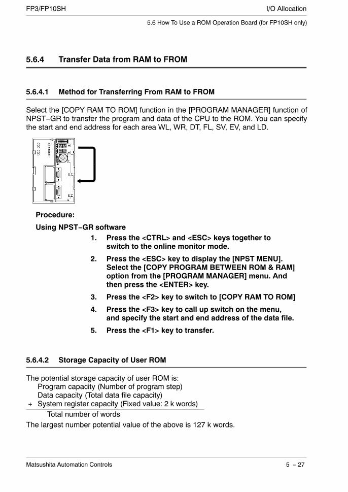
I/O AllocationFP3/FP10SH
5 − 27Matsushita Automation Controls
5.6 How To Use a ROM Operation Board (for FP10SH only)
5.6.4 Transfer Data from RAM to FROM
5.6.4.1 Method for Transferring From RAM to FROM
Select the [COPY RAM TO ROM] function in the [PROGRAM MANAGER] function ofNPST−GR to transfer the program and data of the CPU to the ROM. You can specifythe start and end address for each area WL, WR, DT, FL, SV, EV, and LD.
Procedure:
Using NPST−GR software1. Press the <CTRL> and <ESC> keys together to
switch to the online monitor mode.
2. Press the <ESC> key to display the [NPST MENU].Select the [COPY PROGRAM BETWEEN ROM & RAM]option from the [PROGRAM MANAGER] menu. Andthen press the <ENTER> key.
3. Press the <F2> key to switch to [COPY RAM TO ROM]
4. Press the <F3> key to call up switch on the menu,and specify the start and end address of the data file.
5. Press the <F1> key to transfer.
5.6.4.2 Storage Capacity of User ROM
The potential storage capacity of user ROM is:Program capacity (Number of program step)Data capacity (Total data file capacity)
+ System register capacity (Fixed value: 2 k words)Total number of words
The largest number potential value of the above is 127 k words.
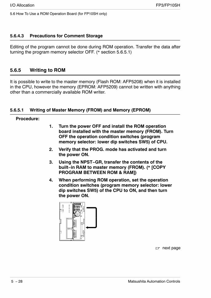
I/O Allocation FP3/FP10SH
5 − 28 Matsushita Automation Controls
5.6 How To Use a ROM Operation Board (for FP10SH only)
5.6.4.3 Precautions for Comment Storage
Editing of the program cannot be done during ROM operation. Transfer the data afterturning the program memory selector OFF. (* section 5.6.5.1)
5.6.5 Writing to ROM
It is possible to write to the master memory (Flash ROM: AFP5208) when it is installedin the CPU, however the memory (EPROM: AFP5209) cannot be written with anythingother than a commercially available ROM writer.
5.6.5.1 Writing of Master Memory (FROM) and Memory (EPROM)
Procedure:
1. Turn the power OFF and install the ROM operationboard installed with the master memory (FROM). TurnOFF the operation condition switches (programmemory selector: lower dip switches SW5) of CPU.
2. Verify that the PROG. mode has activated and turnthe power ON.
3. Using the NPST−GR, transfer the contents of thebuilt−in RAM to master memory (FROM). (* [COPYPROGRAM BETWEEN ROM & RAM])
4. When performing ROM operation, set the operationcondition switches (program memory selector: lowerdip switches SW5) of the CPU to ON, and then turnthe power ON.
next page
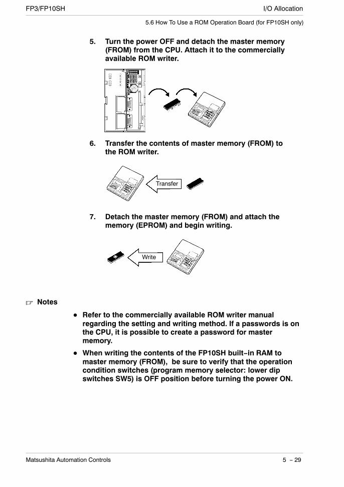
I/O AllocationFP3/FP10SH
5 − 29Matsushita Automation Controls
5.6 How To Use a ROM Operation Board (for FP10SH only)
5. Turn the power OFF and detach the master memory(FROM) from the CPU. Attach it to the commerciallyavailable ROM writer.
6. Transfer the contents of master memory (FROM) tothe ROM writer.
Transfer
7. Detach the master memory (FROM) and attach thememory (EPROM) and begin writing.
Write
Notes
Refer to the commercially available ROM writer manualregarding the setting and writing method. If a passwords is onthe CPU, it is possible to create a password for mastermemory.
When writing the contents of the FP10SH built−in RAM tomaster memory (FROM), be sure to verify that the operationcondition switches (program memory selector: lower dipswitches SW5) is OFF position before turning the power ON.

I/O Allocation FP3/FP10SH
5 − 30 Matsushita Automation Controls
5.6 How To Use a ROM Operation Board (for FP10SH only)
Transfer using the NPST−GR softwareUse the [LOAD TO/FROM ROM WRITER] option of NPST−GR version 4.2 or later todirectly transfer the commercially available ROM writer.
Procedure:
1. In the [NPST CONFIGURATION] menu, press the<SHIFT> and <F6> keys to display the [ROMCONFIG].
<ROM CONFIG> Window
TRANS RATE (bps) [ 9600 Σ 4800 Σ 2400 Σ 1200 Σ 600 Σ 300 ]
DATA LENGTH [ 8 Σ 7 ]
PARITY CHECK [ NO Σ EV Σ OD ]
STOP BIT [ 1 Σ 2 ]
2. Set the transmission rate and communication formatthat matches that for the ROM writer with, and press<F1> to save the settings.
3. Press the <ESC> key, and select [PROGRAMMANAGER] from the [NPST MENU] then select the[LOAD TO/FROM ROM WRITER] option. Press the<ENTER> key.
[LOAD TO/FROM ROM WRITER]
READ WRITE VRFY
INTEL HEX MOTOROLA [S]
SERIAL PORT CENTRNICS PORT FILE
NO PASSWORD WITH PASSWORD
F1 : EXECUTE.
4. Specify the transmission format and connectionmethod appropriate for the ROM writer and thenselect [WRITE]. Press the <F1> key. The data istransfered to the ROM writer.
. next page
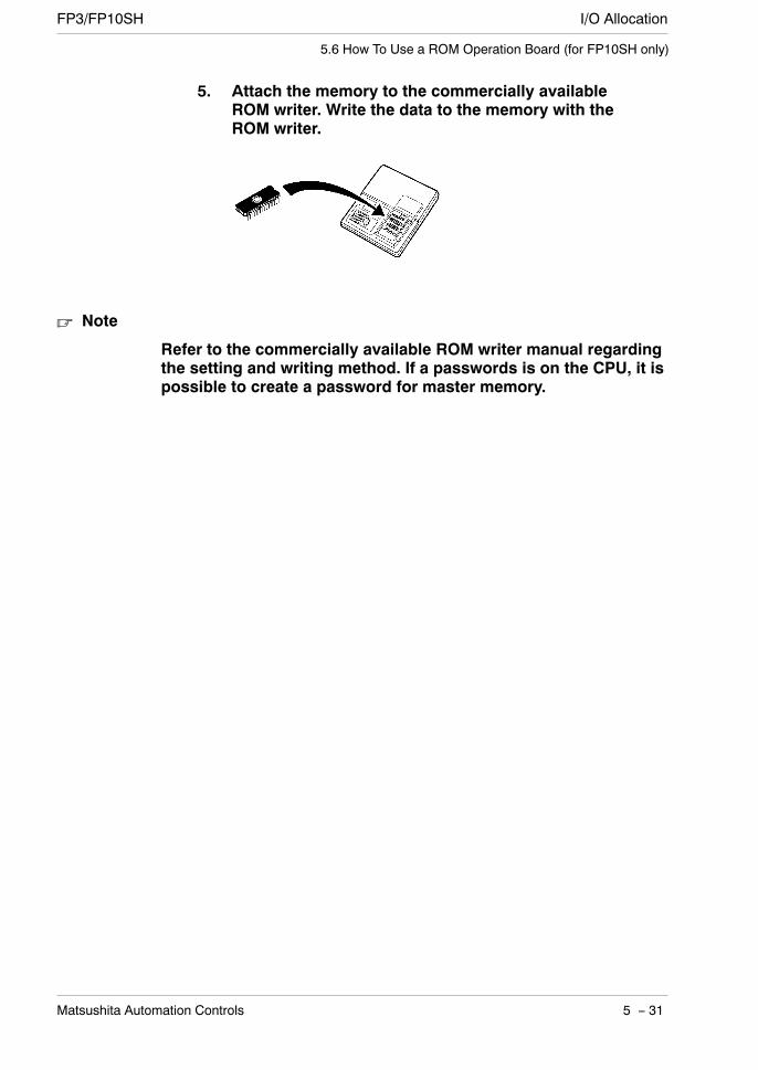
I/O AllocationFP3/FP10SH
5 − 31Matsushita Automation Controls
5.6 How To Use a ROM Operation Board (for FP10SH only)
5. Attach the memory to the commercially availableROM writer. Write the data to the memory with theROM writer.
Note
Refer to the commercially available ROM writer manual regardingthe setting and writing method. If a passwords is on the CPU, it ispossible to create a password for master memory.
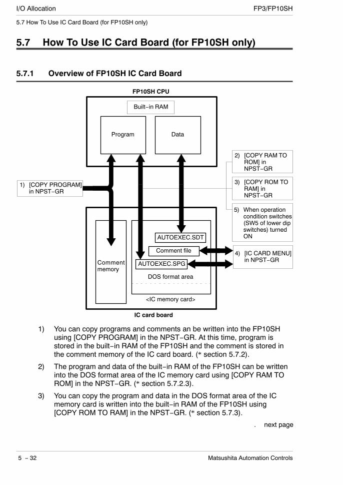
I/O Allocation FP3/FP10SH
5 − 32 Matsushita Automation Controls
5.7 How To Use IC Card Board (for FP10SH only)
5.7 How To Use IC Card Board (for FP10SH only)
5.7.1 Overview of FP10SH IC Card Board
Data
FP10SH CPU
Built−in RAM
Program
1) [COPY PROGRAM]in NPST−GR
4) [IC CARD MENU]in NPST−GRComment
memory
AUTOEXEC.SDT
Comment file
AUTOEXEC.SPG
DOS format area
<IC memory card>
IC card board
2) [COPY RAM TOROM] inNPST−GR
3) [COPY ROM TORAM] inNPST−GR
5) When operationcondition switches(SW5 of lower dipswitches) turnedON
1) You can copy programs and comments an be written into the FP10SHusing [COPY PROGRAM] in the NPST−GR. At this time, program isstored in the built−in RAM of the FP10SH and the comment is stored inthe comment memory of the IC card board. (* section 5.7.2).
2) The program and data of the built−in RAM of the FP10SH can be writteninto the DOS format area of the IC memory card using [COPY RAM TOROM] in the NPST−GR. (* section 5.7.2.3).
3) You can copy the program and data in the DOS format area of the ICmemory card is written into the built−in RAM of the FP10SH using[COPY ROM TO RAM] in the NPST−GR. (* section 5.7.3).
. next page

I/O AllocationFP3/FP10SH
5 − 33Matsushita Automation Controls
5.7 How To Use IC Card Board (for FP10SH only)
4) You can program and comment on the floppy disk or hard disk is writteninto the DOS format area of the IC memory card using [IC CARD MENU]in the NPST−GR. (* section 6.2)
5) If the power is turned ON with the operation condition switches (SW5 oflower dip switches, program memory selector) set to ON, the programand data in the DOS format area of the IC memory card automaticallytransfer into the built−in RAM FP10SH. (* section 5.7.3).
5.7.2 Function of IC Card Board
5.7.2.1 Comment Storage Function
The comment storage function has been added to the FP10SH. Use NPST−GRversion4 to store the comments to the IC memory card.There are three types of comments: the line space comment, the comment sentenceand I/O comment.
Comment
Storage to IC memory cardWith NPST−GRversion 4.2 or greater, by selecting the [PROG& I/O CMT] of the [LOADA PROGRAM TO PLC] menu, the program on the NPST−GR is automaticallycompressed and stored in the built−in RAM and the comment is automaticallycompressed and stored that uses the comment memory of the IC memory card.
Comment
Note
The IC card board (AFP6209A) has a built−in 512kB commentstorage memory.

I/O Allocation FP3/FP10SH
5 − 34 Matsushita Automation Controls
5.7 How To Use IC Card Board (for FP10SH only)
Reading from IC memory cardSelect the [PROG & I/O CMT] option of the [LOAD A PROGRAM FROM PLC] memuto read the data of the built−in RAM and the comment memory to the NPST−GR.
Comment
5.7.2.2 Precautions for Comment Storage
To erase data in the comment memory on the IC memory card, select the [PROG & I/OCMT] option of the program erase function of NPST−GR.When storing the after compressing the comment, approximately 2MB of comment canbe stored. Otherwise, approximately 512kB of comment can be stored.To compress the comment data, you must have the compression software LHA in thecurrent directory and 530kB of open area in the main memory.
5.7.2.3 Transfer Data from RAM to IC Memory Card
Select the [COPY RAM TO ROM] option in the NPST−GR [PROGRAM MANAGER]menu to transfer the program and data of the CPU to the IC memory card. Specify thestart and end address for each area WL, WR, DT, FL, SV, EV, and LD.
next page
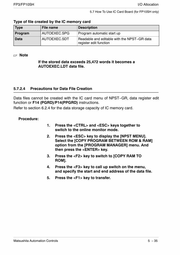
I/O AllocationFP3/FP10SH
5 − 35Matsushita Automation Controls
5.7 How To Use IC Card Board (for FP10SH only)
Type of file created by the IC memory cardType File name Description
Program AUTOEXEC.SPG Program automatic start up
Data AUTOEXEC.SDT Readable and editable with the NPST−GR dataregister edit function
Note
If the stored data exceeds 25,472 words it becomes aAUTOEXEC.LDT data file.
5.7.2.4 Precautions for Data File Creation
Data files cannot be created with the IC card menu of NPST−GR, data register editfunction or F14 (PGRD)/P14(PPGRD) instructions.Refer to section 6.2.4 for the data storage capacity of IC memory card.
Procedure:
1. Press the <CTRL> and <ESC> keys together toswitch to the online monitor mode.
2. Press the <ESC> key to display the [NPST MENU].Select the [COPY PROGRAM BETWEEN ROM & RAM]option from the [PROGRAM MANAGER] menu. Andthen press the <ENTER> key.
3. Press the <F2> key to switch to [COPY RAM TOROM].
4. Press the <F3> key to call up switch on the menu,and specify the start and end address of the data file.
5. Press the <F1> key to transfer.

I/O Allocation FP3/FP10SH
5 − 36 Matsushita Automation Controls
5.7 How To Use IC Card Board (for FP10SH only)
5.7.3 Precautions for IC Memory Card Operation
Once the IC memory card has been installed, be aware that operation varies asdescribed below, depending on the position of the program memory selector (SW5 oflower dip switches) of operation condition switch when the power is turned ON.
Power is turned ONwhen programmemory selector (SW5) of operation conditionswitches set to ON position.When the power is turned ON, the program file name <AUTOEXEC> of the IC memorycard is automatically transferred into the built−in RAM. Note that the previous contentsof the RAM will be erased.
Automatically transferred into the built−in RAM
Power is turned ONwhen programmemory selector (SW5) of operation conditionswitches set to OFF position.Even if the IC memory card is installed, the programming tool read the contents of thebuilt−in RAM.When operating the program that is written into the IC memory card, set the programmemory selector (SW5) of the operation condition switches to ON position and then thepower is turned ON and restart the system.
When the power is turned ON with the program memory selector(SW5) set to OFF, it is possible that the contents of the built−inRAMand the IC memory card will be different.
next page
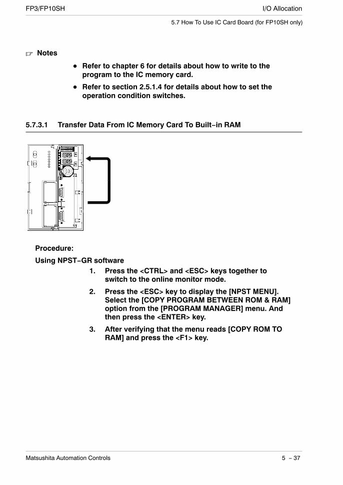
I/O AllocationFP3/FP10SH
5 − 37Matsushita Automation Controls
5.7 How To Use IC Card Board (for FP10SH only)
Notes
Refer to chapter 6 for details about how to write to theprogram to the IC memory card.
Refer to section 2.5.1.4 for details about how to set theoperation condition switches.
5.7.3.1 Transfer Data From IC Memory Card To Built−in RAM
Procedure:
Using NPST−GR software1. Press the <CTRL> and <ESC> keys together to
switch to the online monitor mode.
2. Press the <ESC> key to display the [NPST MENU].Select the [COPY PROGRAM BETWEEN ROM & RAM]option from the [PROGRAM MANAGER] menu. Andthen press the <ENTER> key.
3. After verifying that the menu reads [COPY ROM TORAM] and press the <F1> key.

I/O Allocation FP3/FP10SH
5 − 38 Matsushita Automation Controls
5.7 How To Use IC Card Board (for FP10SH only)

Chapter 6
IC Memory Card
6.1 Overview of IC Memory Card 6 − 3. . . . . . . . . . . . . .
6.2 Configuration of IC Memory Card 6 − 6. . . . . . . . . . .
6.2.1 Program Memory and ExpansionMemory Areas 6 − 6. . . . . . . . . . . . . . . . . . .
6.2.2 IC Memory Card FormattingProcedures 6 − 8. . . . . . . . . . . . . . . . . . . . . .
6.2.3 Procedure to Erase IC MemoryCard 6 − 9. . . . . . . . . . . . . . . . . . . . . . . . . . . .
6.2.4 Data Storage Capacity of IC MemoryCard 6 − 10. . . . . . . . . . . . . . . . . . . . . . . . . . .
6.2.5 Managing IC Memory Card 6 − 11. . . . . . .
6.3 How To Use IC Memory Card 6 − 13. . . . . . . . . . . . .
6.3.1 For Use as Program Memory 6 − 13. . . . . .
6.3.1.1 Writing the Program 6 − 13. . . . . .
6.3.1.2 Reading the Program 6 − 15. . . . .
6.3.2 For Use as Expansion Memory 6 − 19. . . .
6.3.2.1 Outline of ExpansionMemory 6 − 19. . . . . . . . . . . . . . . .
6.3.2.2 Configuration of ExpansionMemory Area 6 − 21. . . . . . . . . . . .

I/O Allocation FP3/FP10SH
6 − 2 Matsushita Automation Controls

I/O AllocationFP3/FP10SH
6 − 3Matsushita Automation Controls
6.1 Overview of IC Memory Card
6.1 Overview of IC Memory Card
The IC memory card is optional memory to be used with the FP10SH. It is not for usewith the FP3. It has two main purposes, saving programs and expanding the data areamemory. One IC memory card has the following three main applications:
− Exclusively for use in program storage
− Exclusively for use in expanding data memory area
− For combined use in program storage and expanding data memory area
For use in program storageThe program is written and saved onto the ICmemory card. The ICmemory card writtedprogram is then used as the program memory.With the NPST−GR, change the name of the file to [AUTOEXEC] and make a copy ofthe file. Then, by turning the power ON while the program memory selection (SW5) ofthe operation condition switch is set to ON position (IC memory card), the programautomatically loads into the built−in RAM and you can begin operation.Execute the F14 (PGRD)/P14 (PPGRD) instruction during RUN and it is possible toswitch the program with the program of any specified file name.
For use in expanding data memory areaSuch things as the data written in the data register of FP10SH are written to the ICmemory card. With this method, the IC memory card can be used as an expandedmemory area can be used for the writing and reading of data by program.When writing data, use the F13 (ICWT)/P13 (PICWT) instruction and when reading datafrom IC memory card, use the F12 (ICRD)/P12 (PICRD) instruction.The FLASH−EEPROM type IC memory card is exclusively for reading.
Note
The IC memory card of SRAM type and FLASH−EEPROM type aresplit into two areas, one for program storage and one forexpanding data memoy.

I/O Allocation FP3/FP10SH
6 − 4 Matsushita Automation Controls
6.1 Overview of IC Memory Card
How the IC memory card is used
F13 (ICWT) instruction(SRAM type only)
F12 (ICRD) instruction
F14 (PGRD) instruction
Programmemory
(built−in RAM)IC memorycard
Program memoryareas
Program 1Program 2Program 3
Program n
Expanded datamemory
Automatic operation whenpower is turned ON
AUTOEXEC.SPG
Operationmemory
Expanded memoryarea
When using the IC memory card as program memory, there are three methods forreading a program:
− Reading automatically when the power is turned ON.
− Reading with the [IC CARD PROGRAM MANAGER] of the NPST−GR.
− Reading with the F14 (PGRD) instruction.
Types of IC memory cardThere are of two types of IC memory cards, the SRAM type, and a FLASH−EEPROMtype. Selection can be made depending on the availability of use.
Type Memory capacity Order number
SRAM type 1MB AIC31000
FLASH−EEPROM type 1MB AIC30010
SRAM type IC memory cardMost suitable for use with data memory area expansionWhen used as expansion memory, use the F13 (ICWT)/P13 (PICWT ) and F12(ICRD)/P12 (PICRD) instructions for freely occurring data reading and data writing asdesired.Equipped with a battery used for data backup.
next page

I/O AllocationFP3/FP10SH
6 − 5Matsushita Automation Controls
6.1 Overview of IC Memory Card
FLASH−EEPROM type IC memory cardSince a backup battery is not necessary it is suited to saving programs.Perform the program writing with in the [IC CARD MANAGER] of NPST−GR.When used as expansion memory, it is limited to reading.
Handling the IC memory cardAvoid high temperature, high humidity and direct sunlight.
Refrain from jolting or exposing the card to rough handling.
Do not allow the card to get wet.
Do not touch or allow foreign objects to contact the connectors.
Do not place in or near flames.
I/O Allocation FP3/FP10SH
6 − 6 Matsushita Automation Controls
6.2 Configuration of IC Memory Card
6.2 Configuration of IC Memory Card
6.2.1 Program Memory and Expansion Memory Areas
The area where the program is saved as is, referred to as the “program area” and thearea used for expansion of data memory is called the “expansion memory area.” It isnecessary to segregate the areas according to IC memory card use.Left over capacity in IC memory card cannot be used.
Exclusive use as program memoryWhen using exclusively for saving programs, it is necessary to use the NPST−GR todesignate the whole IC memory card as program memory area.
SRAM type IC memory card:Format all of the areas of the IC memory card using the [FORMAT IC CARD (SRAM)]of the [IC CARDPROGRAMMANAGER]menu. Refer to the section 6.2.2 for formattingprocedure.
FLASH−EEPROM type IC memory card:Procedure:
1. Erase all of the areas of IC memory card using[ERASE IC CARD(F&SCRAM)] of the [IC CARDPROGRAM MANAGER]. (* section 6.2.3)
2. Use [COPY FILES TO IC CARD (F−EEPROM)] to copythe program from floppy or a hard disk to the ICmemory card.
Note
When copying for a second time, re−execute from procedure 1.
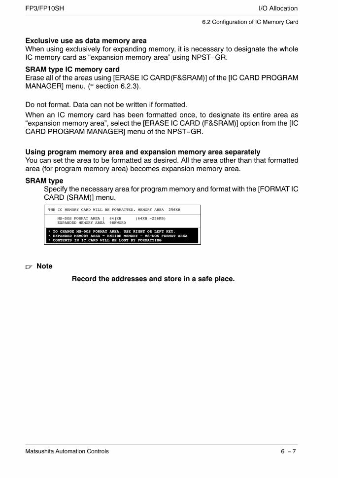
I/O AllocationFP3/FP10SH
6 − 7Matsushita Automation Controls
6.2 Configuration of IC Memory Card
Exclusive use as data memory areaWhen using exclusively for expanding memory, it is necessary to designate the wholeIC memory card as “expansion memory area” using NPST−GR.
SRAM type IC memory cardErase all of the areas using [ERASE IC CARD(F&SRAM)] of the [IC CARD PROGRAMMANAGER] menu. (* section 6.2.3).
Do not format. Data can not be written if formatted.When an IC memory card has been formatted once, to designate its entire area as“expansion memory area”, select the [ERASE IC CARD (F&SRAM)] option from the [ICCARD PROGRAM MANAGER] menu of the NPST−GR.
Using program memory area and expansion memory area separatelyYou can set the area to be formatted as desired. All the area other than that formattedarea (for program memory area) becomes expansion memory area.
SRAM typeSpecify the necessary area for programmemory and format with the [FORMAT ICCARD (SRAM)] menu.
THE IC MEMORY CARD WILL BE FORMATTED. MEMORY AREA 256KB
MS−DOS FORMAT AREA [ 64]KB (64KB −256KB)EXPANDED MEMORY AREA 98KWORD
* TO CHANGE MS−DOS FORMAT AREA, USE RIGHT OR LEFT KEY.* EXPANDED MEMORY AREA = ENTIRE MEMORY − MS−DOS FORMAT AREA* CONTENTS IN IC CARD WILL BE LOST BY FORMATTING
Note
Record the addresses and store in a safe place.

I/O Allocation FP3/FP10SH
6 − 8 Matsushita Automation Controls
6.2 Configuration of IC Memory Card
6.2.2 IC Memory Card Formatting Procedures
SRAM type IC memory cardBefore saving the program, first format a IC memory card for MS−DOS and ensure thatthere is a program memory area for saving the program.
Procedure:
1. Select the [FORMAT IC CARD (SRAM)] option fromthe [IC CARD PROGRAM MANAGER] menu of theNPST−GR software.
2. When the following screen appears, set the formatsize (format area).
THE IC MEMORY CARD WILL BE FORMATTED. MEMORY AREA 256KB
MS−DOS FORMAT AREA [ 64]KB (64KB −256KB)EXPANDED MEMORY AREA 98KWORD
* TO CHANGE MS−DOS FORMAT AREA, USE RIGHT OR LEFT KEY.* EXPANDED MEMORY AREA = ENTIRE MEMORY − MS−DOS FORMAT AREA* CONTENTS IN IC CARD WILL BE LOST BY FORMATTING
3. Press the <F1> key to execute.
FLASH−EEPROM type IC memory cardWhen you copy the programon the disk to the ICmemory card, it simultaneously formatsthe card.
Procedure:
1. Select the [COPY FILES TO IC CARD (F−EEPROM)]option for the FLASH−EEPROM in the [IC CARDPROGRAM MANAGER] menu of the NPST−GRsoftware.
2. When the following screen appears, set the formatsize (format area) and press the <F1> key.
THE IC MEMORY CARD WILL BE FORMATTED. MEMORY AREA 512KB
MS−DOS FORMAT AREA [ 256]KB (64KB −512KB)EXPANDED MEMORY AREA 128KWORD
* TO CHANGE MS−DOS FORMAT AREA, USE RIGHT OR LEFT KEY.* EXPANDED MEMORY AREA = ENTIRE MEMORY − MS−DOS FORMAT AREA* CONTENTS IN IC CARD WILL BE LOST BY FORMATTING
next page
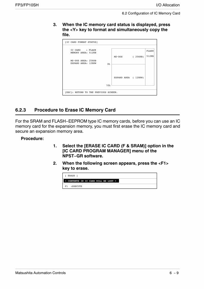
I/O AllocationFP3/FP10SH
6 − 9Matsushita Automation Controls
6.2 Configuration of IC Memory Card
3. When the IC memory card status is displayed, pressthe <Y> key to format and simultaneously copy thefile.
[IC CARD FORMAT STATUS]
IC CARD : FLASHMEMORY AREA: 512KB
MS−DOS AREA: 256KBEXPAND AREA: 128KW
[ESC]: RETURN TO THE PREVIOUS SCREEN.
MS−DOS ( 256KB)
EXPAND AREA ( 128KW)
FLASH
512KB
0h
7fh
6.2.3 Procedure to Erase IC Memory Card
For the SRAM and FLASH−EEPROM type IC memory cards, before you can use an ICmemory card for the expansion memory, you must first erase the IC memory card andsecure an expansion memory area.
Procedure:
1. Select the [ERASE IC CARD (F & SRAM)] option in the[IC CARD PROGRAM MANAGER] menu of theNPST−GR software.
2. When the following screen appears, press the <F1>key to erase.
[ ERASE ]
< CONTENTS IN IC CARD WILL BE LOST >
F1 :EXECUTE FORMATTING
I/O Allocation FP3/FP10SH
6 − 10 Matsushita Automation Controls
6.2 Configuration of IC Memory Card
6.2.4 Data Storage Capacity of IC Memory Card
When storing a program or data in the IC memory card, the data storage capacity is asfollows.
Program onlyTotal number of bytes: program file (*.SPG), annotation comment (*.NCB), line space
comment (*.GYO), and FAT area (see note)Keep the total number of bytes for the files given above less than the MS−DOS formatcapacity.
Note
FAT area:256kB format = 6kB512kB format = 6.5kB1M format = 10kB
Program and I/O commentTotal number of bytes: program file (*.SPG), annotation comment (*.NCB), line space
comment (*.GYO), I/O comment (*.SCM) and FAT areaKeep the total number of bytes for the files given above less than the MS−DOS formatcapacity. The I/O comment changes according to the size of the statements.

I/O AllocationFP3/FP10SH
6 − 11Matsushita Automation Controls
6.2 Configuration of IC Memory Card
6.2.5 Managing IC Memory Card
With theNPST−GR software Ver. 3 or later, there is amenu formanaging the ICmemorycard.[IC CARD PROGRAM MANAGER]
[1. LOAD PROG FROM IC CARD (F&SRAM)][2. LOAD PROGRAM TO IC CARD (SRAM)]
[3. COPY FILES FROM IC CARD (F&SRAM)]
[4. COPY FILES TO IC CARD (SRAM)]
[5. COPY FILES TO IC CARD (F−EEPROM)]
[6. DELETE FILES (SRAM)]
[7. RENAME A FILE (SRAM)]
[8. CHANGE FILE ATTRIBUTE (SRAM)]
[9. ERASE IC CARD (F&SRAM)]
[A. FORMAT IC CARD (SRAM)]
Reading the programs and data stored in the IC memory card (For both the SRAMand FLASH−EEPROM types )
[1. LOAD PROG FROM IC CARD (F & SRAM)]:Selects one of the programs stored on the IC memory card and reads its to theNPST−GR.
[3. COPY FILES FROM IC CARD (F & SRAM)]:Reads the stored files of program or data from the IC memory card and copies itto a floppy disk or (to the hard disk).
To create a copy of the IC memory card, first copy the files of the IC memory onto a disk,then replace the card with a new IC memory card and copy the files from the disk to thenew IC memory card using the [COPY FILES TO IC CARD] option.
Initializing an IC memory card (For both the SRAM and FLASH−EEPROM types)[9. ERASE IC CARD (F & SRAM)]:Clears the entire contents of the IC memory card. Clears all program areasformatted with [A. FORMAT IC CARD (SRAM)], and makes the whole area forexpansion memory.
I/O Allocation FP3/FP10SH
6 − 12 Matsushita Automation Controls
6.2 Configuration of IC Memory Card
Management of SRAM type IC memory cardBefore use, [A. FORMAT IC CARD (SRAM)]:MS−DOS formats the IC memory card, and reserves a program memory area forsaving the program. Any area not reserved as program memory area becomesexpanded memory area.
Writing to the IC memory card,[2. LOAD PROGRAM TO IC CARD (SRAM)]:Writes the program on the NPST−GR to the IC memory card.[4. COPY FILES TO IC CARD (SRAM)]:Copies the contents of a floppy disk or hard disk to the IC memory card. Also, withthis function, you can select multiple programs and write them to the IC memorycard at one time.
Other file management functions[6. DELETE FILES (SRAM)]:Deletes programs on the IC memory card. Also, with this function, you can selectmultiple programs and delete at one time.[7. RENAME A FILE (SRAM)]:Changes the file names and titles of the program on the IC memory card[8. CHANGE FILE ATTRIBUTE (SRAM)]:Exclusively reads the programs on the ICmemory card to read−only files or hiddenfiles.
Writing to FLASH−EEPROM type IC memory card[5. COPY FILES TO IC CARD (F−EEPROM)]:Writing to theFLASH−EEPROMtype ICmemory card is done by copying the entirecontents of a floppy disk or hard disk at one time.With the FLASH−EEPROM type IC memory card, partial editing of contents, filename changes, and erasing cannot be performed. Changes should be made ona disk and then the entire disk should be copied to the IC memory card.
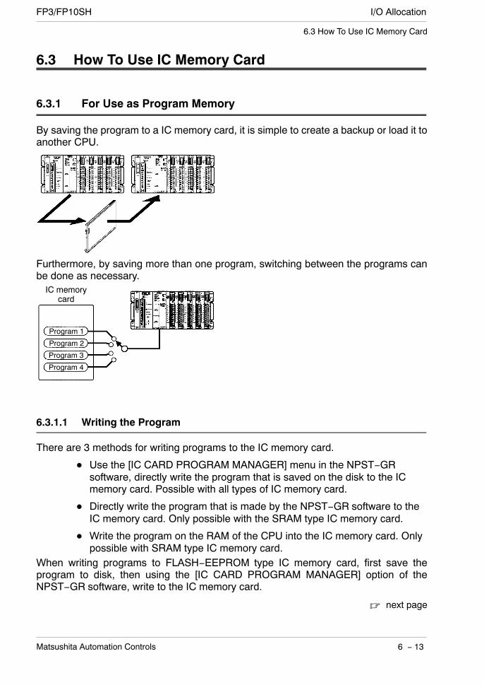
I/O AllocationFP3/FP10SH
6 − 13Matsushita Automation Controls
6.3 How To Use IC Memory Card
6.3 How To Use IC Memory Card
6.3.1 For Use as Program Memory
By saving the program to a IC memory card, it is simple to create a backup or load it toanother CPU.
Furthermore, by saving more than one program, switching between the programs canbe done as necessary.
Program 1
Program 2
Program 3
IC memorycard
Program 4
6.3.1.1 Writing the Program
There are 3 methods for writing programs to the IC memory card.
Use the [IC CARD PROGRAM MANAGER] menu in the NPST−GRsoftware, directly write the program that is saved on the disk to the ICmemory card. Possible with all types of IC memory card.
Directly write the program that is made by the NPST−GR software to theIC memory card. Only possible with the SRAM type IC memory card.
Write the program on the RAM of the CPU into the IC memory card. Onlypossible with SRAM type IC memory card.
When writing programs to FLASH−EEPROM type IC memory card, first save theprogram to disk, then using the [IC CARD PROGRAM MANAGER] option of theNPST−GR software, write to the IC memory card.
next page
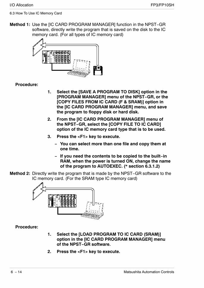
I/O Allocation FP3/FP10SH
6 − 14 Matsushita Automation Controls
6.3 How To Use IC Memory Card
Method 1: Use the [IC CARD PROGRAM MANAGER] function in the NPST−GRsoftware, directly write the program that is saved on the disk to the ICmemory card. (For all types of IC memory card)
Procedure:
1. Select the [SAVE A PROGRAM TO DISK] option in the[PROGRAM MANAGER] menu of the NPST−GR, or the[COPY FILES FROM IC CARD (F & SRAM)] option inthe [IC CARD PROGRAM MANAGER] menu, and savethe program to floppy disk or hard disk.
2. From the [IC CARD PROGRAM MANAGER] menu ofthe NPST−GR, select the [COPY FILE TO IC CARD]option of the IC memory card type that is to be used.
3. Press the <F1> key to execute.
− You can select more than one file and copy them atone time.
− If you need the contents to be copied to the built−inRAM, when the power is turned ON, change the nameof the program to AUTOEXEC. (* section 6.3.1.2)
Method 2: Directly write the program that is made by the NPST−GR software to theIC memory card. (For the SRAM type IC memory card)
Procedure:
1. Select the [LOAD PROGRAM TO IC CARD (SRAM)]option in the [IC CARD PROGRAM MANAGER] menuof the NPST−GR software.
2. Press the <F1> key to execute.
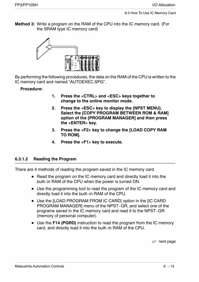
I/O AllocationFP3/FP10SH
6 − 15Matsushita Automation Controls
6.3 How To Use IC Memory Card
Method 3: Write a program on the RAM of the CPU into the IC memory card. (Forthe SRAM type IC memory card)
By performing the following procedures, the data on the RAMof the CPU is written to theIC memory card and named “AUTOEXEC.SPG”.
Procedure:
1. Press the <CTRL> and <ESC> keys together tochange to the online monitor mode.
2. Press the <ESC> key to display the [NPST MENU].Select the [COPY PROGRAM BETWEEN ROM & RAM]option of the [PROGRAM MANAGER] and then pressthe <ENTER> key.
3. Press the <F2> key to change the [LOAD COPY RAMTO ROM].
4. Press the <F1> key to execute.
6.3.1.2 Reading the Program
There are 4 methods of reading the program saved in the IC memory card.
Read the program on the IC memory card and directly load it into thebuilt−in RAM of the CPU when the power is turned ON.
Use the programming tool to read the program of the IC memory card anddirectly load it into the built−in RAM of the CPU.
Use the [LOAD PROGRAM FROM IC CARD] option in the [IC CARDPROGRAM MANAGER] menu of the NPST−GR, and select one of theprograms saved in the IC memory card and read it to the NPST−GR(memory of personal computer).
Use the F14 (PGRD) instruction to read the program from the IC memorycard, and directly load it into the built−in RAM of the CPU.
next page
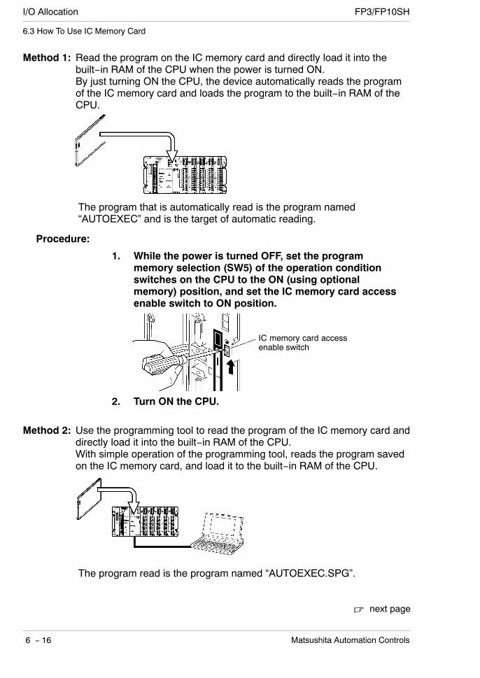
I/O Allocation FP3/FP10SH
6 − 16 Matsushita Automation Controls
6.3 How To Use IC Memory Card
Method 1: Read the program on the IC memory card and directly load it into thebuilt−in RAM of the CPU when the power is turned ON.By just turning ON the CPU, the device automatically reads the programof the IC memory card and loads the program to the built−in RAM of theCPU.
The program that is automatically read is the program named“AUTOEXEC” and is the target of automatic reading.
Procedure:
1. While the power is turned OFF, set the programmemory selection (SW5) of the operation conditionswitches on the CPU to the ON (using optionalmemory) position, and set the IC memory card accessenable switch to ON position.
IC memory card accessenable switch
2. Turn ON the CPU.
Method 2: Use the programming tool to read the program of the IC memory card anddirectly load it into the built−in RAM of the CPU.With simple operation of the programming tool, reads the program savedon the IC memory card, and load it to the built−in RAM of the CPU.
The program read is the program named “AUTOEXEC.SPG”.
next page
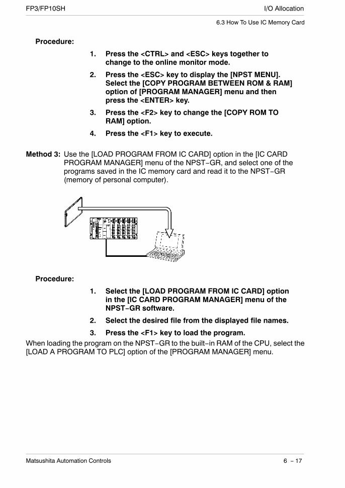
I/O AllocationFP3/FP10SH
6 − 17Matsushita Automation Controls
6.3 How To Use IC Memory Card
Procedure:
1. Press the <CTRL> and <ESC> keys together tochange to the online monitor mode.
2. Press the <ESC> key to display the [NPST MENU].Select the [COPY PROGRAM BETWEEN ROM & RAM]option of [PROGRAM MANAGER] menu and thenpress the <ENTER> key.
3. Press the <F2> key to change the [COPY ROM TORAM] option.
4. Press the <F1> key to execute.
Method 3: Use the [LOAD PROGRAM FROM IC CARD] option in the [IC CARDPROGRAM MANAGER] menu of the NPST−GR, and select one of theprograms saved in the IC memory card and read it to the NPST−GR(memory of personal computer).
Procedure:
1. Select the [LOAD PROGRAM FROM IC CARD] optionin the [IC CARD PROGRAM MANAGER] menu of theNPST−GR software.
2. Select the desired file from the displayed file names.
3. Press the <F1> key to load the program.When loading the program on the NPST−GR to the built−in RAM of the CPU, select the[LOAD A PROGRAM TO PLC] option of the [PROGRAM MANAGER] menu.

I/O Allocation FP3/FP10SH
6 − 18 Matsushita Automation Controls
6.3 How To Use IC Memory Card
Method 4: Use the F14 (PGRD) instruction to read the program from the IC memorycard and directly load it into the built−in RAM of the CPU.
STEP 1
STEP 2
STEP 3
STEP 4F14 (PGRD) instruction
IC memorycard
By first saving the programs you desire on the IC memory card, you can use the F14(PGRD) instruction in the program, to switch a program while in the RUN mode (whilein operation).
The following details the describe the program after executing F14 (PGRD) instruction.
The program will continue executing until the END instruction is executed.
The CPU enters the PROG. mode and the program is read from the ICmemory card and load to the built−in RAM of the CPU.
The CPU automatically switches to the RUN mode, and the new programexecutes.
Program ExampleWith F14 (PGRD) instruction, specify a saved file name by the NPST−GR to call up theprogram of from IC memory card.
F14 PGRD, DT 100
“STEP1”
For the program above, the contents (“STEP 1”) stored in DT100 is the file name usedto call up the program.To store the program name to registers such as DT100, you can write it withalphanumeric code using F0 (MV) or F1 (DMV) instruction, or you can write it with ASCIIconversion using F95 (ASC) instruction. For more details, refer to the programmingmanual.
Note
There are dangers involved when switching programs while in theRUN mode. Carefully read the section regarding the F14 (PGRD)instruction in the programming manual.
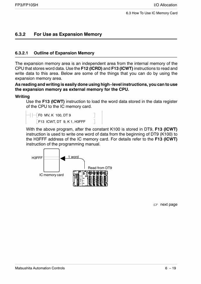
I/O AllocationFP3/FP10SH
6 − 19Matsushita Automation Controls
6.3 How To Use IC Memory Card
6.3.2 For Use as Expansion Memory
6.3.2.1 Outline of Expansion Memory
The expansion memory area is an independent area from the internal memory of theCPU that stores word data. Use the F12 (ICRD) and F13 (ICWT) instructions to read andwrite data to this area. Below are some of the things that you can do by using theexpansion memory area.As reading andwriting is easily doneusinghigh−level instructions, you can tousethe expansion memory as external memory for the CPU.
WritingUse the F13 (ICWT) instruction to load the word data stored in the data registerof the CPU to the IC memory card.
F0 MV, K 100, DT 9
F13 ICWT, DT 9, K 1, H3FFF
With the above program, after the constant K100 is stored in DT9, F13 (ICWT)instruction is used to write one word of data from the beginning of DT9 (K100) tothe H3FFF address of the IC memory card. For details refer to the F13 (ICWT)instruction of the programming manual.
H3FFF
ICmemory card
1 word
Read from DT9
next page
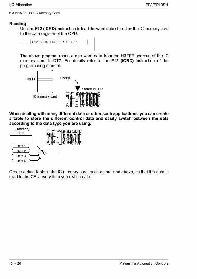
I/O Allocation FP3/FP10SH
6 − 20 Matsushita Automation Controls
6.3 How To Use IC Memory Card
ReadingUse the F12 (ICRD) instruction to load theword data stored on the ICmemory cardto the data register of the CPU.
F12 ICRD, H3FFF, K 1, DT 7
The above program reads a one word data from the H3FFF address of the ICmemory card to DT7. For details refer to the F12 (ICRD) instruction of theprogramming manual.
H3FFF
ICmemory card
1 word
Stored in DT7
When dealing with many different data or other such applications, you can createa table to store the different control data and easily switch between the dataaccording to the data type you are using.
Data 1
Data 2
Data 3
Data 4
IC memorycard
Create a data table in the IC memory card, such as outlined above, so that the data isread to the CPU every time you switch data.

I/O AllocationFP3/FP10SH
6 − 21Matsushita Automation Controls
6.3 How To Use IC Memory Card
6.3.2.2 Configuration of Expansion Memory Area
Areas of the IC memory card that are not formatted can be used as expansion memoryarea.Oneword (two bytes) can be stored in one address. As the following example illustrates,in a 512kB area, data of 262,143 words can be stored.(512× 1024) bytes
2=262,143 words
In the expansion memory area, the addresses are numbered by word units and,regardless of the size of the formatted area, the starting address is numbered as 0 (H0).For example, the addresses for a 512kB (256 k words) area are from as H0 to H3FFFE.
Example: When a 512kB of SRAM type IC memory card is designated asexpansion memory (unformatted).
Expansion memory area(262,143 words)
Address H0
H3FFFE
512kB

I/O Allocation FP3/FP10SH
6 − 22 Matsushita Automation Controls
6.3 How To Use IC Memory Card
Chapter 7
Self−Diagnostic and Troubleshooting
7.1 Self−Diagnostic Function 7 − 3. . . . . . . . . . . . . . . . . .
7.1.1 Status Indicator LEDs on CPU 7 − 3. . . . .
7.1.2 Operation When an Error Occurs 7 − 4. . .
7.1.2.1 Allowing Duplicated Output 7 − 4.
7.1.2.2 Continuing After An OperationError 7 − 4. . . . . . . . . . . . . . . . . . . .
7.2 Troublesooting 7 − 5. . . . . . . . . . . . . . . . . . . . . . . . . . .
7.2.1 If the ERROR LED Lights 7 − 5. . . . . . . . . .
7.2.2 If the ALARM LED Lights 7 − 7. . . . . . . . . .
7.2.3 If the LED (POWER) of Power SupplyUnit Does Not Light 7 − 7. . . . . . . . . . . . . . .
7.2.4 If Outputting Does Not Occur asDesired 7 − 8. . . . . . . . . . . . . . . . . . . . . . . . .
7.2.5 If a Communication Error AppearsWhen Using NPST−GR 7 − 10. . . . . . . . . .
7.2.6 If a Protect Error MessageAppears 7 − 11. . . . . . . . . . . . . . . . . . . . . . . .

I/O Allocation FP3/FP10SH
7 − 2 Matsushita Automation Controls
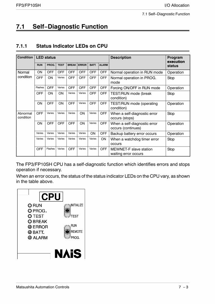
I/O AllocationFP3/FP10SH
7 − 3Matsushita Automation Controls
7.1 Self−Diagnostic Function
7.1 Self−Diagnostic Function
7.1.1 Status Indicator LEDs on CPU
Condition LED status Description Programexecution
RUN PROG. TEST BREAK ERROR BATT. ALARMexecutionstatus
Normal ON OFF OFF OFF OFF OFF OFF Normal operation in RUN mode Operationcondition OFF ON Varies OFF OFF OFF OFF Normal operation in PROG.
modeStop
Flashes OFF Varies OFF OFF OFF OFF Forcing ON/OFF in RUN mode OperationOFF ON ON Varies Varies OFF OFF TEST/RUN mode (break
condition)Stop
ON OFF ON OFF Varies OFF OFF TEST/RUN mode (operatingcondition)
Operation
Abnormalcondition
OFF Varies Varies Varies ON Varies OFF When a self-diagnostic erroroccurs (stops)
Stop
ON OFF OFF OFF ON Varies OFF When a self-diagnostic erroroccurs (continues)
Operation
Varies Varies Varies Varies Varies ON OFF Backup battery error occurs OperationVaries Varies Varies Varies Varies Varies ON When a watchdog timer error
occursStop
OFF Flashes Varies OFF Varies Varies OFF MEWNET-F slave stationwaiting error occurs
Stop
The FP3/FP10SH CPU has a self-diagnostic function which identifies errors and stopsoperation if necessary.When an error occurs, the status of the status indicator LEDs on the CPU vary, as shownin the table above.
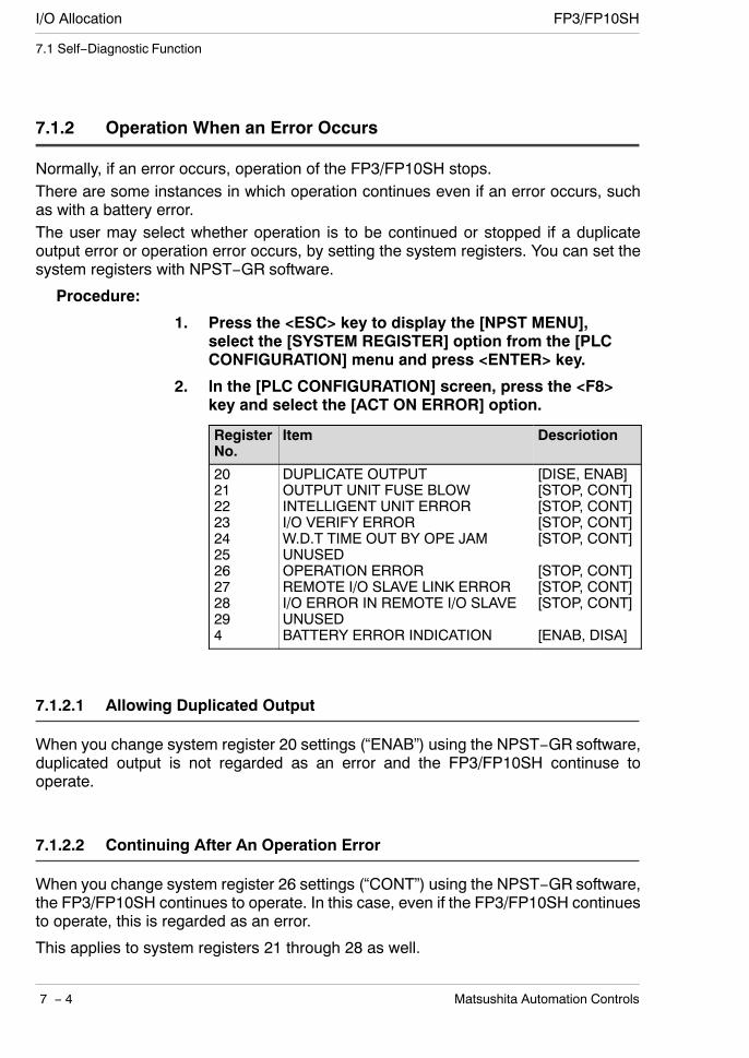
I/O Allocation FP3/FP10SH
7 − 4 Matsushita Automation Controls
7.1 Self−Diagnostic Function
7.1.2 Operation When an Error Occurs
Normally, if an error occurs, operation of the FP3/FP10SH stops.There are some instances in which operation continues even if an error occurs, suchas with a battery error.The user may select whether operation is to be continued or stopped if a duplicateoutput error or operation error occurs, by setting the system registers. You can set thesystem registers with NPST−GR software.
Procedure:
1. Press the <ESC> key to display the [NPST MENU],select the [SYSTEM REGISTER] option from the [PLCCONFIGURATION] menu and press <ENTER> key.
2. In the [PLC CONFIGURATION] screen, press the <F8>key and select the [ACT ON ERROR] option.
RegisterNo.
Item Descriotion
202122232425262728294
DUPLICATE OUTPUTOUTPUT UNIT FUSE BLOWINTELLIGENT UNIT ERRORI/O VERIFY ERRORW.D.T TIME OUT BY OPE JAMUNUSEDOPERATION ERRORREMOTE I/O SLAVE LINK ERRORI/O ERROR IN REMOTE I/O SLAVEUNUSEDBATTERY ERROR INDICATION
[DISE, ENAB][STOP, CONT][STOP, CONT][STOP, CONT][STOP, CONT]
[STOP, CONT][STOP, CONT][STOP, CONT]
[ENAB, DISA]
7.1.2.1 Allowing Duplicated Output
When you change system register 20 settings (“ENAB”) using the NPST−GR software,duplicated output is not regarded as an error and the FP3/FP10SH continuse tooperate.
7.1.2.2 Continuing After An Operation Error
When you change system register 26 settings (“CONT”) using the NPST−GR software,the FP3/FP10SH continues to operate. In this case, even if the FP3/FP10SH continuesto operate, this is regarded as an error.
This applies to system registers 21 through 28 as well.
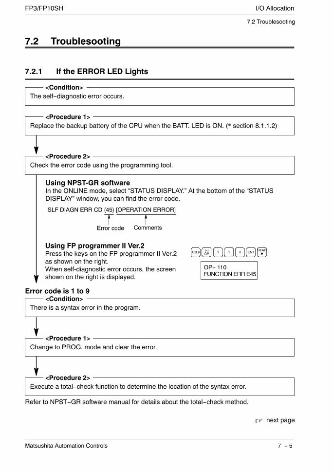
I/O AllocationFP3/FP10SH
7 − 5Matsushita Automation Controls
7.2 Troublesooting
7.2 Troublesooting
7.2.1 If the ERROR LED Lights
The self−diagnostic error occurs.<Condition>
Replace the backup battery of the CPU when the BATT. LED is ON. (* section 8.1.1.2)<Procedure 1>
Check the error code using the programming tool.<Procedure 2>
Error code is 1 to 9
There is a syntax error in the program.<Condition>
Change to PROG. mode and clear the error.<Procedure 1>
Execute a total−check function to determine the location of the syntax error.<Procedure 2>
Refer to NPST−GR software manual for details about the total−check method.
next page
Using NPST-GR softwareIn the ONLINE mode, select “STATUS DISPLAY.” At the bottom of the “STATUSDISPLAY” window, you can find the error code.
OP− 110FUNCTIONERRE45
READ(−)ACLR OP 0 ENT
SLF DIAGN ERR CD (45) [OPERATION ERROR]
11
Error code Comments
Using FP programmer II Ver.2Press the keys on the FP programmer II Ver.2as shown on the right.When self-diagnostic error occurs, the screenshown on the right is displayed.

I/O Allocation FP3/FP10SH
7 − 6 Matsushita Automation Controls
7.2 Troublesooting
Error code is 20 or higher
A self−diagnostic error other than a syntax error has occurred.<Condition>
Use the programming tool in PROG. mode to clear the error.<Procedure 1>
Follow the procedures described in the table of error codes (* section Appendix F).<Procedure 2>
Note
When an operation error (error code 45) occurs, the address atwhich the error occurred is stored in special data registers (FP3:DT9017 and DT9018, FP10SH: DT90017 and DT90018). If thishappens, monitor the address at which the error occurred beforecancelling the error.
Using FP programmer II Ver.2Press the keys as follows. Error code 43 and higher can be cleared.
In the PROG. mode, the power supply can be turned OFF and then ON again to clearthe error, but all of the contents of the operation memory except hold type data arecleared.An error can also be cleared by executing a self−diagnostic error set instruction F148(ERR)/P148 (PERR).
For version 4.3 or earlier FP3 CPU, change to the PROG. mode and turn the powerOFF and ON to clear the error condition.
Using NPST-GR softwarePress the <F3> key in the “STATUS DISPLAY” menu described on the previous page.Error code 43 and higher can be cleared.
(−)ACLR OP ENT11 2 SHIFT
SC(DELT)INST
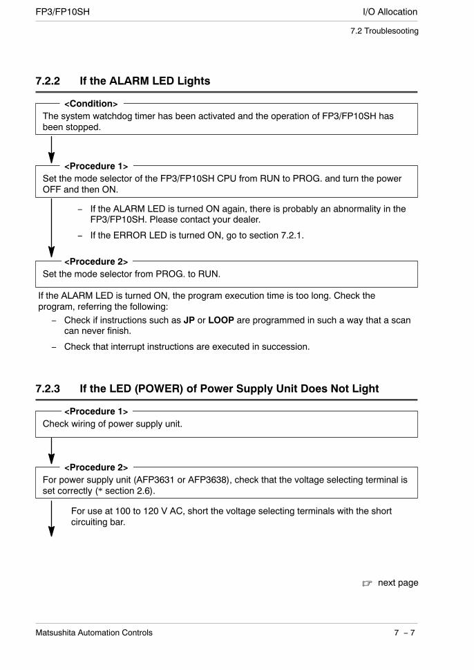
I/O AllocationFP3/FP10SH
7 − 7Matsushita Automation Controls
7.2 Troublesooting
7.2.2 If the ALARM LED Lights
The system watchdog timer has been activated and the operation of FP3/FP10SH hasbeen stopped.
<Condition>
Set the mode selector of the FP3/FP10SH CPU from RUN to PROG. and turn the powerOFF and then ON.
<Procedure 1>
Set the mode selector from PROG. to RUN.<Procedure 2>
7.2.3 If the LED (POWER) of Power Supply Unit Does Not Light
Check wiring of power supply unit.<Procedure 1>
For power supply unit (AFP3631 or AFP3638), check that the voltage selecting terminal isset correctly (* section 2.6).
<Procedure 2>
next page
− If the ALARM LED is turned ON again, there is probably an abnormality in theFP3/FP10SH. Please contact your dealer.
− If the ERROR LED is turned ON, go to section 7.2.1.
If the ALARM LED is turned ON, the program execution time is too long. Check theprogram, referring the following:
− Check if instructions such as JP or LOOP are programmed in such a way that a scancan never finish.
− Check that interrupt instructions are executed in succession.
For use at 100 to 120 V AC, short the voltage selecting terminals with the shortcircuiting bar.
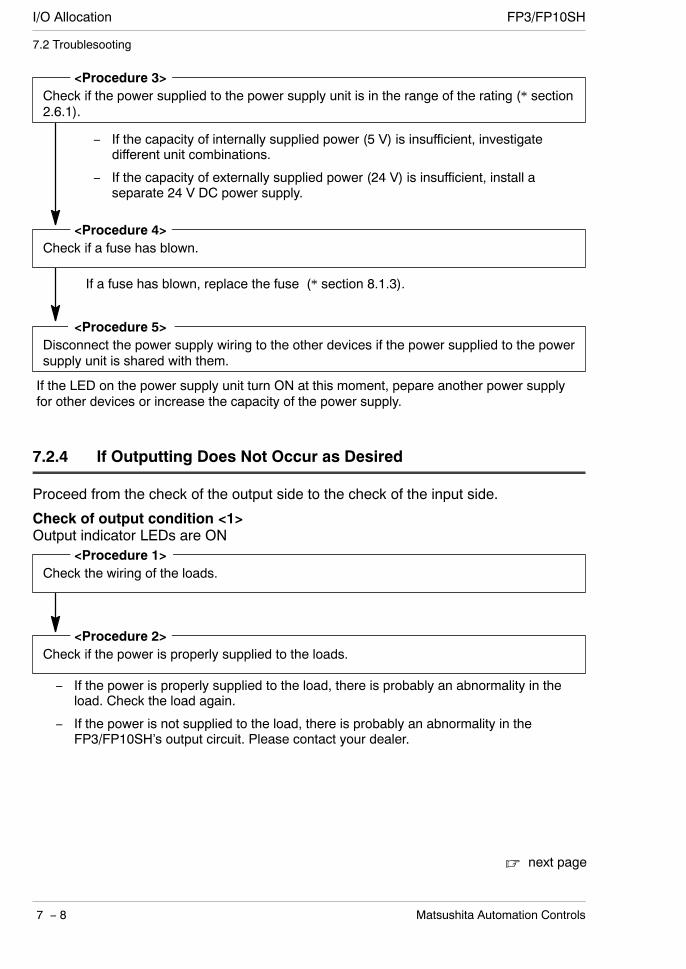
I/O Allocation FP3/FP10SH
7 − 8 Matsushita Automation Controls
7.2 Troublesooting
Check if the power supplied to the power supply unit is in the range of the rating (* section2.6.1).
<Procedure 3>
Check if a fuse has blown.<Procedure 4>
Disconnect the power supply wiring to the other devices if the power supplied to the powersupply unit is shared with them.
<Procedure 5>
7.2.4 If Outputting Does Not Occur as Desired
Proceed from the check of the output side to the check of the input side.
Check of output condition <1>Output indicator LEDs are ON
Check the wiring of the loads.<Procedure 1>
Check if the power is properly supplied to the loads.<Procedure 2>
next page
− If the capacity of internally supplied power (5 V) is insufficient, investigatedifferent unit combinations.
− If the capacity of externally supplied power (24 V) is insufficient, install aseparate 24 V DC power supply.
If a fuse has blown, replace the fuse (* section 8.1.3).
If the LED on the power supply unit turn ON at this moment, pepare another power supplyfor other devices or increase the capacity of the power supply.
− If the power is properly supplied to the load, there is probably an abnormality in theload. Check the load again.
− If the power is not supplied to the load, there is probably an abnormality in theFP3/FP10SH’s output circuit. Please contact your dealer.

I/O AllocationFP3/FP10SH
7 − 9Matsushita Automation Controls
7.2 Troublesooting
Check of output condition <2>Output indicator LEDs are OFF
Monitor the output condition using a programming tool.<Procedure 1>
Forcing ON the output using forcing I/O function.<Procedure 2>
Check of input condition <1>Input indicator LEDs are OFF
Check the wiring of the input devices.<Procedure 1>
Check that the power is properly supplied to the input terminals.<Procedure 2>
Check of input condition <2>Input indicator LEDs are ON
Monitor the input condition using a programming tool.<Procedure>
− If the output monitored is turned ON, there is probably a duplicated output error.
− If the output indicator LED is turned ON, go to input condition check.
− If the output indicator LED remains OFF, there is probably an abnormality in theoutput unit. Please contact your dealer.
− If the power is properly supplied to the input terminal, there is probably an abnormalityin the input unit. Please contact your dealer.
− If the power is not properly supplied to the input terminal, there is probably anabnormality in the input device or input power supply. Check the input device andinput power supply.
− If the input monitored is OFF, there is probably an abnormality with the input unit.Please contact your dealer.
− If the input monitored is ON, check the program again.Also, check the leakage current at the input devices (e.g., two−wire type sensor) andcheck the program again referring the following:Check for the duplicated use of output. Check the program flow when a controlinstruction such as MC or JP is used.Check the settings of the I/O allocation.
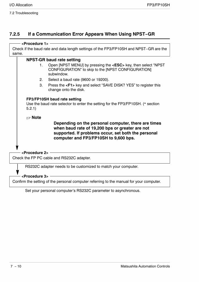
I/O Allocation FP3/FP10SH
7 − 10 Matsushita Automation Controls
7.2 Troublesooting
7.2.5 If a Communication Error Appears When Using NPST−GR
Check if the baud rate and data length settings of the FP3/FP10SH and NPST−GR are thesame.
<Procedure 1>
Check the FP PC cable and RS232C adapter.<Procedure 2>
Confirm the setting of the personal computer referring to the manual for your computer.<Procedure 3>
NPST-GR baud rate setting1. Open [NPST MENU] by pressing the <ESC> key, then select “NPST
CONFIGURATION” to skip to the [NPST CONFIGURATION]subwindow.
2. Select a baud rate (9600 or 19200).3. Press the <F1> key and select “SAVE DISK? YES” to register this
change onto the disk.
FP3/FP10SH baud rate settingUse the baud rate selector to enter the setting for the FP3/FP10SH. (* section5.2.1)
NoteDepending on the personal computer, there are timeswhen baud rate of 19,200 bps or greater are notsupported. If problems occur, set both the personalcomputer and FP3/FP10SH to 9,600 bps.
RS232C adapter needs to be customized to match your computer.
Set your personal computer’s RS232C parameter to asynchronous.
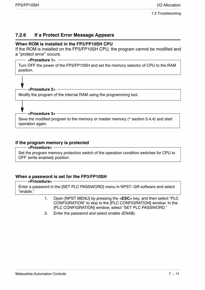
I/O AllocationFP3/FP10SH
7 − 11Matsushita Automation Controls
7.2 Troublesooting
7.2.6 If a Protect Error Message Appears
When ROM is installed in the FP3/FP10SH CPUIf the ROM is installed on the FP3/FP10SH CPU, the program cannot be modified anda “protect error” occurs.
Turn OFF the power of the FP3/FP10SH and set the memory selector of CPU to the RAMposition.
<Procedure 1>
Modify the program of the internal RAM using the programming tool.<Procedure 2>
Save the modified program to the memory or master memory (* section 5.4.4) and startoperation again.
<Procedure 3>
If the program memory is protected
Set the program memory protection switch of the operation condition switches for CPU toOFF (write enabled) position.
<Procedure>
When a password is set for the FP3/FP10SH
Enter a password in the [SET PLC PASSWORD] menu in NPST−GR software and select“enable.”
<Procedure>
1. Open [NPST MENU] by pressing the <ESC> key, and then select “PLCCONFIGRATION” to skip to the [PLC CONFIGRATION] window. In the[PLC CONFIGRATION] window, select “SET PLC PASSWORD.”
2. Enter the password and select enable (ENAB).

I/O Allocation FP3/FP10SH
7 − 12 Matsushita Automation Controls
7.2 Troublesooting
Chapter 8
Maintenance
8.1 Replacement of Spare Parts 8 − 3. . . . . . . . . . . . . . .
8.1.1 Replacement of Backup Battery 8 − 3. . . .
8.1.1.1 Lifetime of Backup Battery 8 − 3.
8.1.1.2 Replacement Method ofBattery 8 − 4. . . . . . . . . . . . . . . . . .
8.1.2 Battery of IC Memory Card 8 − 6. . . . . . . . .
8.1.2.1 Battery Lifetime 8 − 6. . . . . . . . . . .
8.1.2.2 Replacement Method ofBattery 8 − 7. . . . . . . . . . . . . . . . . .
8.1.3 Replacement of Fuse for PowerSupply Unit 8 − 8. . . . . . . . . . . . . . . . . . . . . .
8.1.3.1 Replacement Method ofFuse 8 − 8. . . . . . . . . . . . . . . . . . . .
8.1.4 Removable Terminal Block for Inputand Output Units 8 − 9. . . . . . . . . . . . . . . . .
8.1.5 Replacement of Relay for OutputUnit 8 − 9. . . . . . . . . . . . . . . . . . . . . . . . . . . . .
8.1.5.1 Replacement Method ofRelay 8 − 9. . . . . . . . . . . . . . . . . . .
8.1.6 Replacement of Fuse for OutputUnit 8 − 11. . . . . . . . . . . . . . . . . . . . . . . . . . . .
8.1.6.1 Replacement Method ofFuse 8 − 11. . . . . . . . . . . . . . . . . . .
8.2 Preventive Maintenance 8 − 12. . . . . . . . . . . . . . . . . .

I/O Allocation FP3/FP10SH
8 − 2 Matsushita Automation Controls
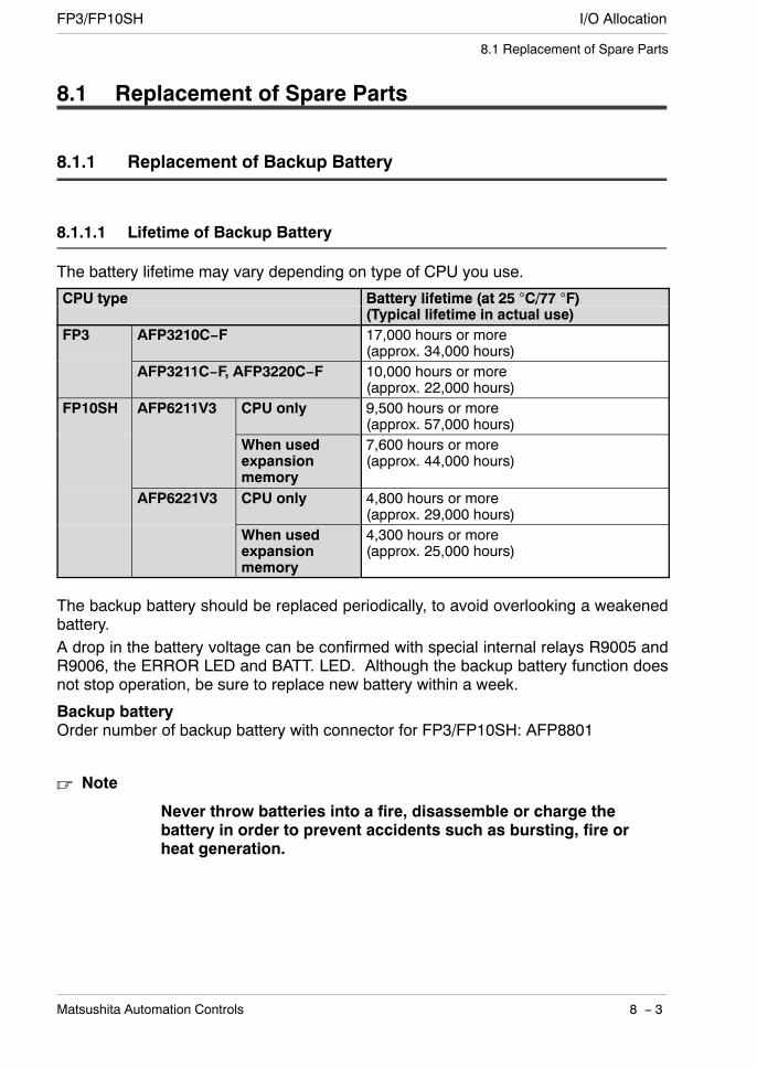
I/O AllocationFP3/FP10SH
8 − 3Matsushita Automation Controls
8.1 Replacement of Spare Parts
8.1 Replacement of Spare Parts
8.1.1 Replacement of Backup Battery
8.1.1.1 Lifetime of Backup Battery
The battery lifetime may vary depending on type of CPU you use.
CPU type Battery lifetime (at 25 °C/77 °F)CPU type Battery lifetime (at 25 C/77 F)(Typical lifetime in actual use)
FP3 AFP3210C−F 17,000 hours or more(approx. 34,000 hours)
AFP3211C−F, AFP3220C−F 10,000 hours or more(approx. 22,000 hours)
FP10SH AFP6211V3 CPU only 9,500 hours or more(approx. 57,000 hours)
When usedexpansionmemory
7,600 hours or more(approx. 44,000 hours)
AFP6221V3 CPU only 4,800 hours or more(approx. 29,000 hours)
When usedexpansionmemory
4,300 hours or more(approx. 25,000 hours)
The backup battery should be replaced periodically, to avoid overlooking a weakenedbattery.A drop in the battery voltage can be confirmed with special internal relays R9005 andR9006, the ERROR LED and BATT. LED. Although the backup battery function doesnot stop operation, be sure to replace new battery within a week.
Backup batteryOrder number of backup battery with connector for FP3/FP10SH: AFP8801
Note
Never throw batteries into a fire, disassemble or charge thebattery in order to prevent accidents such as bursting, fire orheat generation.
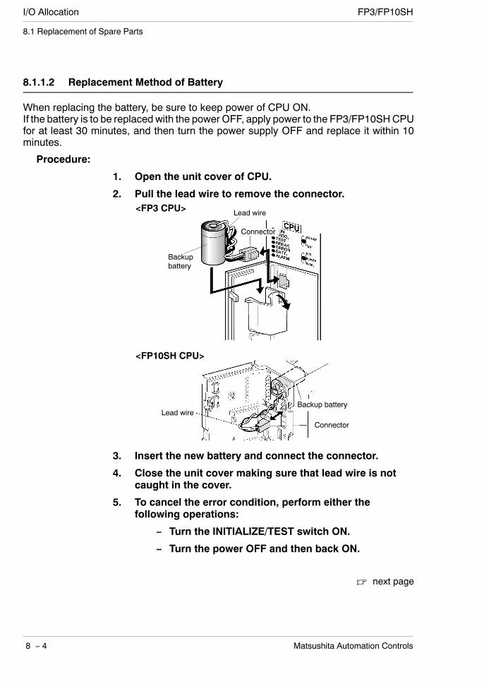
I/O Allocation FP3/FP10SH
8 − 4 Matsushita Automation Controls
8.1 Replacement of Spare Parts
8.1.1.2 Replacement Method of Battery
When replacing the battery, be sure to keep power of CPU ON.If the battery is to be replaced with the power OFF, apply power to the FP3/FP10SHCPUfor at least 30 minutes, and then turn the power supply OFF and replace it within 10minutes.
Procedure:
1. Open the unit cover of CPU.
2. Pull the lead wire to remove the connector.<FP3 CPU>
<FP10SH CPU>
Connector
Lead wire
Backupbattery
Backup battery
Connector
Lead wire
3. Insert the new battery and connect the connector.
4. Close the unit cover making sure that lead wire is notcaught in the cover.
5. To cancel the error condition, perform either thefollowing operations:
− Turn the INITIALIZE/TEST switch ON.
− Turn the power OFF and then back ON.
next page

I/O AllocationFP3/FP10SH
8 − 5Matsushita Automation Controls
8.1 Replacement of Spare Parts
Note
Be aware that if you turn ON the initialize/test switch, the dataregister of hold type and other contents of operation memory willalso be initialized. (For the FP10SH, by using the system register,you can set it so that it does not clear the operation memory. Formore details, refer to the system register on programmingmanual.)
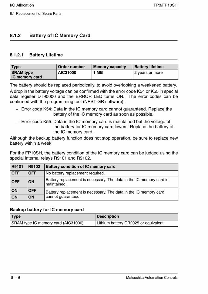
I/O Allocation FP3/FP10SH
8 − 6 Matsushita Automation Controls
8.1 Replacement of Spare Parts
8.1.2 Battery of IC Memory Card
8.1.2.1 Battery Lifetime
Type Order number Memory capacity Battery lifetimeSRAM typeIC memory card
AIC31000 1 MB 2 years or more
The battery should be replaced periodically, to avoid overlooking a weakened battery.A drop in the battery voltage can be confirmed with the error code K54 or K55 in specialdata register DT90000 and the ERROR LED turns ON. The error codes can beconfirmed with the programming tool (NPST-GR software).
− Error code K54: Data in the IC memory card cannot guaranteed. Replace thebattery of the IC memory card as soon as possible.
− Error code K55: Data in the IC memory card is maintained but the voltage ofthe battery for IC memory card lowers. Replace the battery ofthe IC memory card.
Although the backup battery function does not stop operation, be sure to replace newbattery within a week.
For the FP10SH, the battery condition of the IC memory card can be judged using thespecial internal relays R9101 and R9102.
R9101 R9102 Battery condition of IC memory card
OFF OFF No battery replacement required.
OFF ON Battery replacement is necessary. The data in the IC memory card ismaintained.
ON OFF Battery replacement is necessary. The data in the IC memory cardON ON
Battery replacement is necessary. The data in the IC memory cardcannot guaranteed.
Backup battery for IC memory cardType Description
SRAM type IC memory card (AIC31000) Lithium battery CR2025 or equivalent

I/O AllocationFP3/FP10SH
8 − 7Matsushita Automation Controls
8.1 Replacement of Spare Parts
8.1.2.2 Replacement Method of Battery
The battery can be replaced while the power supply of FP10SH is turned ON.
Procedure:
1. Open the unit cover of CPU.
2. Set the IC memory card access enable switch to OFFposition. The IC memory card access LED turns OFF.
Eject button
IC memory card
IC memory card access LED
IC memory card access enable switch
3. Pull out the IC memory card.
4. Use the screwdriver supplied with the IC memorycard to remove the screw on the card side.
Cover
Screw
Battery
IC memory card
5. Remove the battery and insert the new battery.
6. Attach the cover and tighten the screw in place.
7. Insert the IC memory card to the slot for the card inCPU until the eject button sticks out.
8. Set the IC memory card access enable switch to ONposition.
Note
If you are replacing the battery after turning OFF the powersupply of FP10SH, then steps 2 and 8 are unnecessary. Thoughbe sure to finish the replacement procedure within 10 minutes.

I/O Allocation FP3/FP10SH
8 − 8 Matsushita Automation Controls
8.1 Replacement of Spare Parts
8.1.3 Replacement of Fuse for Power Supply Unit
8.1.3.1 Replacement Method of Fuse
Be sure to turn OFF the power to the FP3 and then replace fuse.
Fuse
Fuse holder
Power supply unit
Procedure:
1. Remove the fuse holder with a flat-head screwdriver.
2. Replace the fuse with a new one.
3. Attach the fuse holder by pressing it in.
Replacement fuse for power supply unitFuses are for the FP3 power supply unit only. Be sure to specify the appropriate ordernumber given below.
Description Order number
2A type (FP3 power supply unit: AFP3631, AFP3634) AFP88021
4A type (FP3 power supply unit: AFP3638) AFP88022
Note
Always have the power supply turned OFF while replacing afuse.
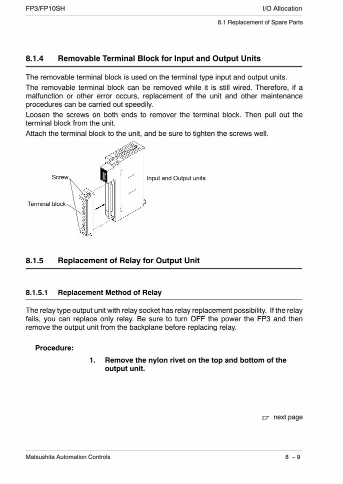
I/O AllocationFP3/FP10SH
8 − 9Matsushita Automation Controls
8.1 Replacement of Spare Parts
8.1.4 Removable Terminal Block for Input and Output Units
The removable terminal block is used on the terminal type input and output units.The removable terminal block can be removed while it is still wired. Therefore, if amalfunction or other error occurs, replacement of the unit and other maintenanceprocedures can be carried out speedily.Loosen the screws on both ends to remover the terminal block. Then pull out theterminal block from the unit.Attach the terminal block to the unit, and be sure to tighten the screws well.
Screw
Terminal block
Input and Output units
8.1.5 Replacement of Relay for Output Unit
8.1.5.1 Replacement Method of Relay
The relay type output unit with relay socket has relay replacement possibility. If the relayfails, you can replace only relay. Be sure to turn OFF the power the FP3 and thenremove the output unit from the backplane before replacing relay.
Procedure:
1. Remove the nylon rivet on the top and bottom of theoutput unit.
next page

I/O Allocation FP3/FP10SH
8 − 10 Matsushita Automation Controls
8.1 Replacement of Spare Parts
2. Insert a flat-head screwdriver into the side slot of theunit and remove the front case by rotating thescrewdriver.Nylon rivet
Flat-head screwdriver
Output unit
3. Pull the PC board out of the case.
PC board
Output unit
4. Remove the failed relay from the socket and insert anew one.
5. Follow the above steps in reverse order toreassemble the unit.
Replacement relayBe sure to specify the appropriate order number given below.
Output unit order number Relay order numberAFP33203−F APC33125
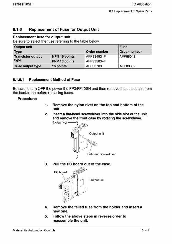
I/O AllocationFP3/FP10SH
8 − 11Matsushita Automation Controls
8.1 Replacement of Spare Parts
8.1.6 Replacement of Fuse for Output Unit
Replacement fuse for output unitBe sure to select the fuse referring to the table below.Output unit FuseType Order number Order numberTransistor output NPN 16 points AFP33483−F AFP88042ptype PNP 16 points AFP33583−FTriac output type 16 points AFP33703 AFP88032
8.1.6.1 Replacement Method of Fuse
Be sure to turn OFF the power the FP3/FP10SH and then remove the output unit fromthe backplane before replacing fuses.
Procedure:
1. Remove the nylon rivet on the top and bottom of theunit.
2. Insert a flat-head screwdriver into the side slot of the unitand remove the front case by rotating the screwdriver.Nylon rivet
Flat-head screwdriver
Output unit
3. Pull the PC board out of the case.
PC board
Output unit
4. Remove the failed fuse from the holder and insert anew one.
5. Follow the above steps in reverse order toreassemble the unit.

I/O Allocation FP3/FP10SH
8 − 12 Matsushita Automation Controls
8.2 Preventive Maintenance
8.2 Preventive Maintenance
Although the FP3/FP10SH system has been designed in such a way to minimizemaintenance and offer troublefree operation, several maintenance aspects should betaken into consideration.If preventive maintenance is performed periodically, you will minimize the possibility ofsystem malfunctions.
Inspection item Inspection description Basis of judgement ReferencePower supplyunit
Check POWER LED onpower supply unit
Normal if ON Section 2.6u t
Power supply unit Periodic replacement(approx. 20,000 hoursoperation)
CPU display Check RUN LED ON in RUN state Section 2.4,d
p yCheck ERROR LED Normal if OFF
,2.5 and 7.1
Check ALARM LED Normal if OFFCheck BATT. LED Normal if OFF
Input/output unitdisplay
Check input/outputdisplay LED
Normal if ON during ON,and OFF during OFF
Section 2.8
Installationcondition
Backplane mountinglooseness
Securely mounted Section 4.1co d t o
Looseness and/or play inunit
Connectioncondition
Looseness of terminalscrew
No looseness Section 4.1co d t o
Proximity of connection inpinch terminal
Pinched parallel
Connector looseness Locked inConnection condition ofexpansion cable
Connector section is notloose
Power supplyvoltage of powersupply unit
Voltage betweenterminals
AFP3631 and AFP3638:85 to 132 V AC or 170to 264 V AC
Section 4.2
pp yAFP3634: 16.8 to 28.8 V
DCPower supplyvoltagefor input/output
Voltage betweenterminals
Within the specified rangeof each unit
Section 2.9 to2.11
Ambienti
Ambient temperature 0 to 55 °C/32 to 131 °F Section 4.1environment Ambient humidity 30 to 85 % RH
Operating condition No dust or corrosive gasBackup battery Battey for CPU Regular replacement Section 8.1.1p y
Battery for IC memorycard
Regular replacement Section 8.1.2
Fuse Fuse of power supply unit Regular replacement Section 8.1.3Fuse of output unit Regular replacement Section 8.1.6

Appendix A
Performance Specifications
A.1 FP10SH Performance Specifications A − 3. . . . . . . .
A.2 FP3 Performance Specifications A − 6. . . . . . . . . . .

Performance Specifications FP3/FP10SH
A − 2 Matsushita Automation Controls
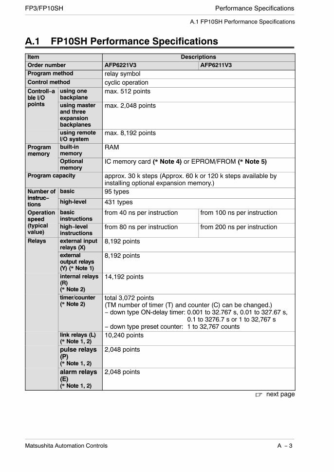
Performance SpecificationsFP3/FP10SH
A − 3Matsushita Automation Controls
A.1 FP10SH Performance Specifications
A.1 FP10SH Performance SpecificationsItem DescriptionsOrder number AFP6221V3 AFP6211V3Program method relay symbolControl method cyclic operationControll−able I/O
using onebackplane
max. 512 pointsble I/Opoints using master
and threeexpansionbackplanes
max. 2,048 points
using remoteI/O system
max. 8,192 points
Programmemory
built-inmemory
RAMmemory
Optionalmemory
IC memory card (* Note 4) or EPROM/FROM (* Note 5)
Program capacity approx. 30 k steps (Approx. 60 k or 120 k steps available byinstalling optional expansion memory.)
Number ofinstruc−
basic 95 typesinstruc−tions high-level 431 types
Operationspeed
basicinstructions
from 40 ns per instruction from 100 ns per instructionspeed(typicalvalue)
high−levelinstructions
from 80 ns per instruction from 200 ns per instruction
Relays external inputrelays (X)
8,192 points
externaloutput relays(Y) (* Note 1)
8,192 points
internal relays(R)(* Note 2)
14,192 points
timer/counter(* Note 2)
total 3,072 points(TM number of timer (T) and counter (C) can be changed.)− down type ON-delay timer: 0.001 to 32.767 s, 0.01 to 327.67 s,
0.1 to 3276.7 s or 1 to 32,767 s− down type preset counter: 1 to 32,767 counts
link relays (L)(* Note 1, 2)
10,240 points
pulse relays(P)(* Note 1, 2)
2,048 points
alarm relays(E)(* Note 1, 2)
2,048 points
next page

Performance Specifications FP3/FP10SH
A − 4 Matsushita Automation Controls
A.1 FP10SH Performance Specifications
Item Descriptions
Order number AFP6221V3 AFP6211V3Memoryareas
data registers(DT) (* Note 2)
10,240 words
file registers(FL) (* Note 2)
32,765 words
link dataregisters (LD)(* Note 2, 3)
8,448 words
timer/counterset value area(SV)
3,072 words
timer/counterelapsed valuearea (EV)
3,072 words
indexregisters(I)
14 words (I0 to ID) (with bank switching, 224 words portions canbe used)
Differential points(DF and DF/)
unlimited number of points
Auxiliary timer unlimited number of points, down type timer (0.01 to 327.67 s)Master control relaypoints (MCR)
256 points (when using the 90 k step expansion memory, up to atotal of 512 points can be used for the no. 1 and 2 programs)
Number of labels(JP and LOOP)
256 points (when using the 90 k step expansion memory, up to atotal of 512 points can be used for the no. 1 and 2 programs)
Number of step ladder(* Note 2)
1,000 steps (can only be used for the no. 1 program)
Number of subroutine 100 subroutines (can only be used for the no. 1 program)Number of interruptprogram
25 program (can only be used for the no. 1 program)
Comment input function available (either the IC memory card board or ROM operationboard are required)
Sampling trace function max. 1,000 samples (16 contacts and 3 words/sample)Clock/calendar function year, month, day, hour, minute, second and day of weekLink functions PC link, computer link, data transfer, remote programming and
MODEM capabilitySelf-diagnostic function watching dog timer, memory malfunction detection, I/O malfunction
detection, backup battery malfunction detection, program syntaxcheck, etc.
Other functions program edition during RUN, forced ON/OFF, interrupt input, testrun and constant scan
Memorybackuptime
CPU only min. 4,800 hours(typical : approx. 29,000 hours)
min. 9,500 hours(typical : approx. 57,000 hours)
time(lithiumbatterystoragetime)
when usedexpansionmemory
min. 4,300 hours (* Note 6)(typical : approx. 25,000 hours)
min. 7,600 hours (* Note 6)(typical : approx. 44,000 hours)
next page
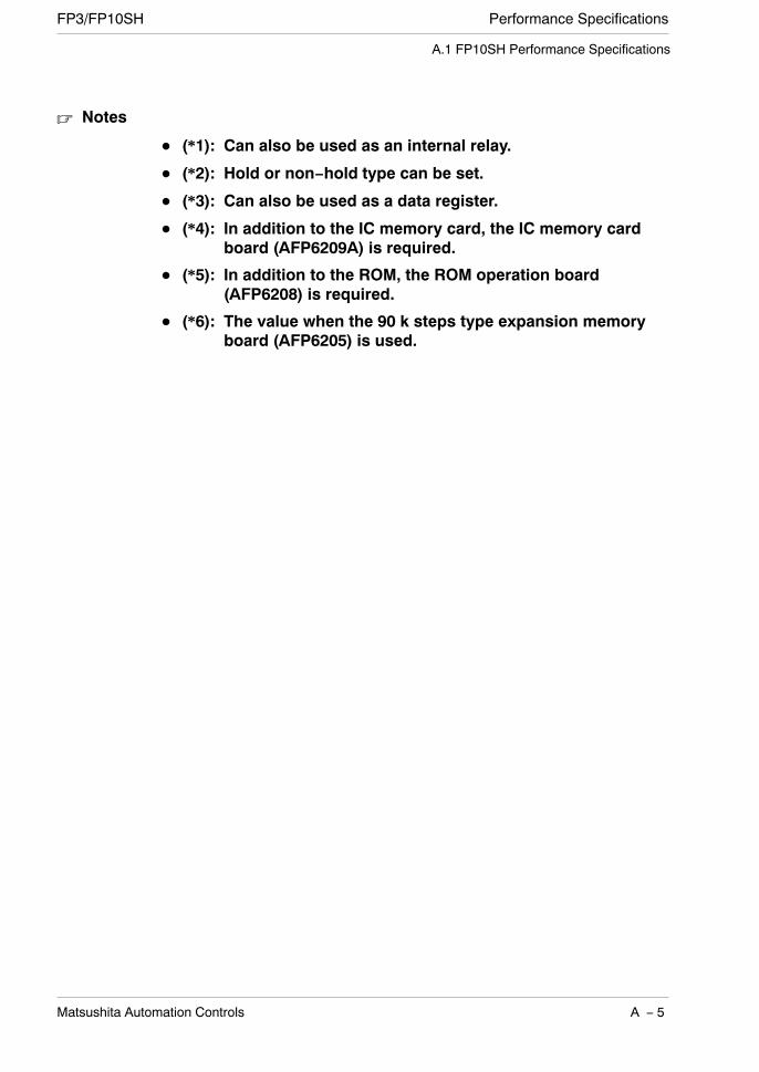
Performance SpecificationsFP3/FP10SH
A − 5Matsushita Automation Controls
A.1 FP10SH Performance Specifications
Notes
(*1): Can also be used as an internal relay.
(*2): Hold or non−hold type can be set.
(*3): Can also be used as a data register.
(*4): In addition to the IC memory card, the IC memory cardboard (AFP6209A) is required.
(*5): In addition to the ROM, the ROM operation board(AFP6208) is required.
(*6): The value when the 90 k steps type expansion memoryboard (AFP6205) is used.
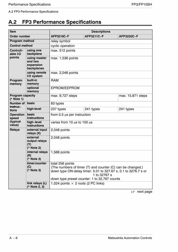
Performance Specifications FP3/FP10SH
A − 6 Matsushita Automation Controls
A.2 FP3 Performance Specifications
A.2 FP3 Performance Specifications
Item Descriptions
Order number AFP3210C−F AFP3211C−F AFP3220C−FProgram method relay symbolControl method cyclic operationControll−able I/O
using onebackplane
max. 512 pointsable I/Opoints using master
and twoexpansionbackplanes
max. 1,536 points
using remoteI/O system
max. 2,048 points
Programmemory
built-inmemory
RAMmemory
optionalmemory
EPROM/EEPROM
Program capacity(* Note 1)
max. 9,727 steps max. 15,871 steps
Number ofinstruc−
basic 83 typesinstruc−tions high-level 237 types 241 types 241 types
Operationspeed
basicinstructions
from 0.5 μs per instructionspeed(typicalvalue)
high−levelinstructions
varies from 10 μs to 100 μs
Relays external inputrelays (X)
2,048 points
externaloutput relays(Y)(* Note 2)
2,048 points
internal relays(R)(* Note 3)
1,568 points
timer/counter(C)(* Note 3)
total 256 points(The numbers of timer (T) and counter (C) can be changed.)down type ON-delay timer: 0.01 to 327.67 s, 0.1 to 3276.7 s or
1 to 32767 sdown type preset counter: 1 to 32,767 counts
link relays (L)(* Note 2, 3)
1,024 points× 2 roots (2 PC links)
next page
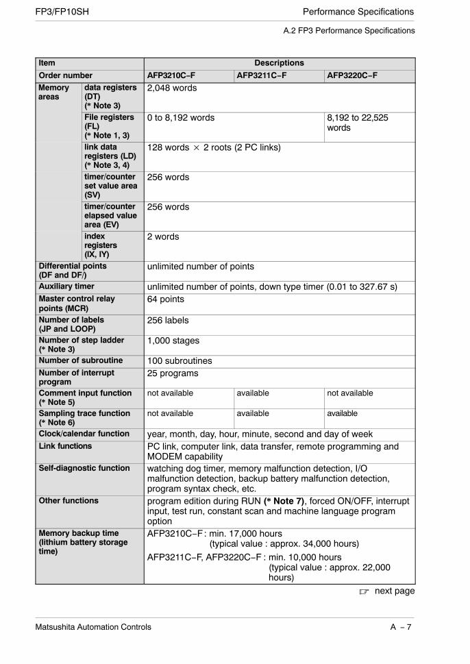
Performance SpecificationsFP3/FP10SH
A − 7Matsushita Automation Controls
A.2 FP3 Performance Specifications
Item Descriptions
Order number AFP3210C−F AFP3211C−F AFP3220C−FMemoryareas
data registers(DT)(* Note 3)
2,048 words
File registers(FL)(* Note 1, 3)
0 to 8,192 words 8,192 to 22,525words
link dataregisters (LD)(* Note 3, 4)
128 words× 2 roots (2 PC links)
timer/counterset value area(SV)
256 words
timer/counterelapsed valuearea (EV)
256 words
indexregisters(IX, IY)
2 words
Differential points(DF and DF/)
unlimited number of points
Auxiliary timer unlimited number of points, down type timer (0.01 to 327.67 s)Master control relaypoints (MCR)
64 points
Number of labels(JP and LOOP)
256 labels
Number of step ladder(* Note 3)
1,000 stages
Number of subroutine 100 subroutinesNumber of interruptprogram
25 programs
Comment input function(* Note 5)
not available available not available
Sampling trace function(* Note 6)
not available available available
Clock/calendar function year, month, day, hour, minute, second and day of weekLink functions PC link, computer link, data transfer, remote programming and
MODEM capabilitySelf-diagnostic function watching dog timer, memory malfunction detection, I/O
malfunction detection, backup battery malfunction detection,program syntax check, etc.
Other functions program edition during RUN (* Note 7), forced ON/OFF, interruptinput, test run, constant scan and machine language programoption
Memory backup time(lithium battery storagetime)
AFP3210C−F : min. 17,000 hours(typical value : approx. 34,000 hours)
AFP3211C−F, AFP3220C−F : min. 10,000 hours(typical value : approx. 22,000hours)
next page
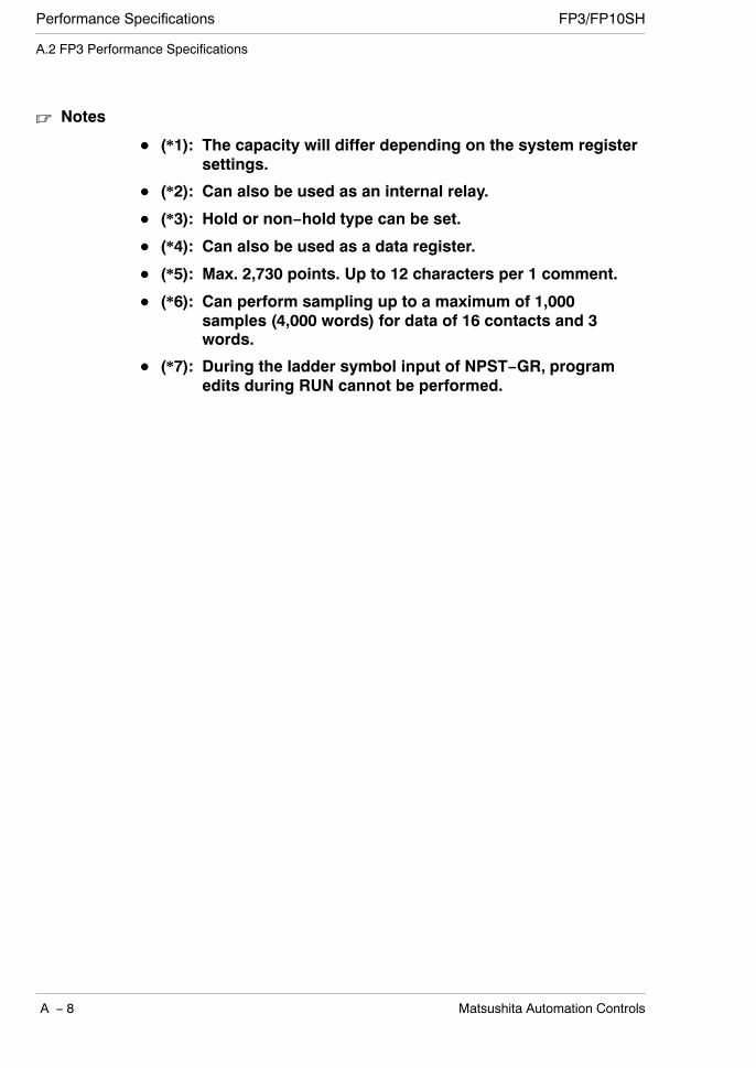
Performance Specifications FP3/FP10SH
A − 8 Matsushita Automation Controls
A.2 FP3 Performance Specifications
Notes
(*1): The capacity will differ depending on the system registersettings.
(*2): Can also be used as an internal relay.
(*3): Hold or non−hold type can be set.
(*4): Can also be used as a data register.
(*5): Max. 2,730 points. Up to 12 characters per 1 comment.
(*6): Can perform sampling up to a maximum of 1,000samples (4,000 words) for data of 16 contacts and 3words.
(*7): During the ladder symbol input of NPST−GR, programedits during RUN cannot be performed.
Appendix B
Table of System Registers
B.1 System Registers B − 3. . . . . . . . . . . . . . . . . . . . . . . .
B.2 Content of System Register Settings B − 6. . . . . . . .
B.3 Table of System Registers (for FP3) B − 10. . . . . .
B.4 Table of System Registers (for FP10SH) B − 16. .
B.4.1 Operation of DF Instruction BetweenMC and MCE Instructions B − 22. . . . . . .

Performance Specifications FP3/FP10SH
B − 2 Matsushita Automation Controls
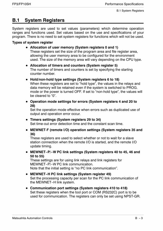
Performance SpecificationsFP3/FP10SH
B − 3Matsushita Automation Controls
B.1 System Registers
B.1 System Registers
System registers are used to set values (parameters) which determine operationranges and functions used. Set values based on the use and specifications of yourprogram. There is no need to set system registers for functions which will not be used.
Types of system registerAllocation of user memory (System registers 0 and 1)These registers set the size of the program area and file register area,allowing the user memory area to be configured for the environmentused. The size of the memory area will vary depending on the CPU type.
Allocation of timers and counters (System register 5)The number of timers and counters is set by specifying the startingcounter number.
Hold/non-hold type settings (System registers 6 to 18)When these registers are set to “hold type”, the values in the relays anddata memory will be retained even if the system is switched to PROG.mode or the power is turned OFF. If set to “non-hold type”, the values willbe cleared to “0”.
Operation mode settings for errors (System registers 4 and 20 to28)Set the operation mode effective when errors such as duplicated use ofoutput and operation error occur.
Timers settings (System registers 29 to 34)Set time-out error detection time and the constant scan time.
MEWNET-F (remote I/O) operation settings (System registers 35 and36)These registers are used to select whether or not to wait for a slavestation connection when the remote I/O is started, and the remote I/Oupdate timing.
MEWNET−P/−WPC link settings (System registers 40 to 45, 46 and50 to 55)These settings are for using link relays and link registers forMEWNET−P/−WPC link communication.Note that the initial setting is “no PC link communication”.
MEWNET−H PC link settings (System register 49)Set the processing capacity per scan for the PC link communication ofthe MEWNET−H link system.
Communication port settings (System registers 410 to 418)Set these registers when the tool port or COM (RS232C) port is to beused for communication. The registers can only be set using NPST-GR.
Performance Specifications FP3/FP10SH
B − 4 Matsushita Automation Controls
B.1 System Registers
Checking and changing system register settingsIf you are going to use a value which is already set (the value which appears when read),there is no need to write it again.
Using NPST-GR softwareProcedure:
1. Set the mode selector of the FP3/FP10SH CPU toPROG.
2. Select the “SYSTEM REGISTER” in “PLCCONFIGURATION” option from the NPST menu.
3. Select the function to be set in the the “SYSTEMREGISTER” in “PLC CONFIGURATION” screen. Thevalue set in the selected system register will appear.
4. To change a set value, write the new value asindicated in the system register table.
5. After setting, press <F1> key and type <Y> key tosave the revised settings to the FP3/FP10SH CPU.
Using FP programmer II Ver.2Procedure:
1. Set the mode selector of the FP3/FP10SH CPU toPROG.
2. Press the keys on the FP programmer II Ver.2, asshown below.ACLR OP
(−)ENT05
3. Specify the register number (e.g. No.26) for theparameter to be set and read the parameter.The value set in the selected register (e.g. No.26) willbe displayed.
2 6READ
Β
4. To change the set value, press the <CLR (clear)> keyand write the new value as indicated in the systemregister table using decimal (K) or hexdecimal (H)constant.
Note
Be aware that the FP programmer II Ver.2 cannot make settingsat the FP10SH system register.

Performance SpecificationsFP3/FP10SH
B − 5Matsushita Automation Controls
B.1 System Registers
Precautions for system register settingSytem register settings are effective from the time they are set.However, modem connection settings become effective when the power is turned OFFand ON.When the initialized operation is performed, all set system register values will beinitialized.
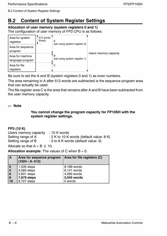
Performance Specifications FP3/FP10SH
B − 6 Matsushita Automation Controls
B.2 Content of System Register Settings
B.2 Content of System Register SettingsAllocation of user memory (system registers 0 and 1)The configuration of user memory of FP3 CPU is as follows:
Area for systemregisters
Area for sequenceprogram
Area for machinelanguage program
512 words(fixed) A
(set using system register 0)
B(set using system register 1)
Area for fileregisters
C
Users memory capacity
Be sure to set the A and B (system registers 0 and 1) as even numbers.The area remaining in A after 512 words are subtracted is the sequence program areathat can actually be used.The file register area C is the area that remains after A and B have been subtracted fromthe user memory capacity.
Note
You cannot change the program capacity for FP10SH with thesystem register settings.
FP3 (10 K)Users memory capacity : 10 K wordsSetting range of A : 2 K to 10 K words (default value: 8 K)Setting range of B : 0 to 8 K words (default value: 0)Allocate so that A + B≦ 10.Allocation example: The values of C when B = 0.
A Area for sequence program(1024×A−512)
Area for file registers (C)
246810
1,535 steps3,583 steps5,631 steps7,679 steps9,727 steps
8,189 words6,141 words4,093 words2,045 words0 words
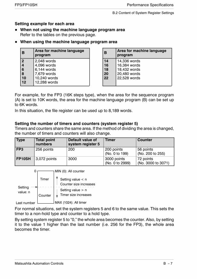
Performance SpecificationsFP3/FP10SH
B − 7Matsushita Automation Controls
B.2 Content of System Register Settings
Setting example for each areaWhen not using the machine language program areaRefer to the tables on the previous page.
When using the machine language program area
B Area for machine languageprogram B Area for machine language
program
24681012
2,048 words4,096 words6,144 words7,679 words10,240 words12,288 words
1416182022
14,336 words16,384 words18,432 words20,480 words22,528 words
For example, for the FP3 (16K steps type), when the area for the sequence program(A) is set to 10K words, the area for the machine language program (B) can be set upto 6K words.In this situation, the file register can be used up to 8,189 words.
Setting the number of timers and counters (system register 5)Timers and counters share the same area. If the method of dividing the area is changed,the number of timers and counters will also change.
Type Total pointnumbers
Default value ofsystem register 5
Timer Counter
FP3 256 points 200 200 points(No. 0 to 199)
56 points(No. 200 to 255)
FP10SH 3,072 points 3000 3000 points(No. 0 to 2999)
72 points(No. 3000 to 3071)
Setting value < nCounter size increases
Setting value > nTimer size increases
0
Last number
Settingvalue: n
Timer
Counter
MIN (0): All counter
MAX (1024): All timer
For normal situations, set the system registers 5 and 6 to the same value. This sets thetimer to a non-hold type and counter to a hold type.By setting system register 5 to “0,” the whole area becomes the counter. Also, by settingit to the value 1 higher than the last number (i.e. 256 for the FP3), the whole areabecomes the timer.
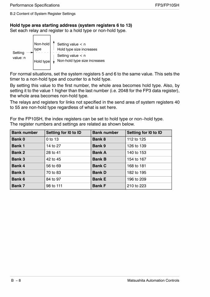
Performance Specifications FP3/FP10SH
B − 8 Matsushita Automation Controls
B.2 Content of System Register Settings
Hold type area starting address (system registers 6 to 13)Set each relay and register to a hold type or non-hold type.
Setting value < nHold type size increases
Setting value < nNon-hold type size increases
Settingvalue: n
Non-holdtype
Hold type
For normal situations, set the system registers 5 and 6 to the same value. This sets thetimer to a non-hold type and counter to a hold type.By setting this value to the first number, the whole area becomes hold type. Also, bysetting it to the value 1 higher than the last number (i.e. 2048 for the FP3 data register),the whole area becomes non-hold type.The relays and registers for links not specified in the send area of system registers 40to 55 are non-hold type regardless of what is set here.
For the FP10SH, the index registers can be set to hold type or non−hold type.The register numbers and settings are related as shown below.
Bank number Setting for I0 to ID Bank number Setting for I0 to ID
Bank 0 0 to 13 Bank 8 112 to 125
Bank 1 14 to 27 Bank 9 126 to 139
Bank 2 28 to 41 Bank A 140 to 153
Bank 3 42 to 45 Bank B 154 to 167
Bank 4 56 to 69 Bank C 168 to 181
Bank 5 70 to 83 Bank D 182 to 195
Bank 6 84 to 97 Bank E 196 to 209
Bank 7 98 to 111 Bank F 210 to 223
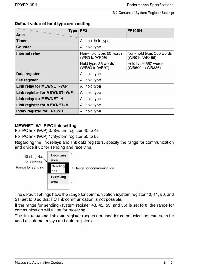
Performance SpecificationsFP3/FP10SH
B − 9Matsushita Automation Controls
B.2 Content of System Register Settings
Default value of hold type area setting
TypeArea
FP3 FP10SH
Timer All non−hold type
Counter All hold type
Internal relay Non−hold type: 60 words(WR0 to WR59)
Non−hold type: 500 words(WR0 to WR499)
Hold type: 38 words(WR60 to WR97)
Hold type: 387 words(WR500 to WR886)
Data register All hold type
File register All hold type
Link relay for MEWNET−W/P All hold type
Link register for MEWNET−W/P All hold type
Link relay for MEWNET−H All hold type
Link register for MEWNET−H All hold type
Index register for FP10SH All hold type
MEWNET−W/−P PC link settingFor PC link (W/P) 0: System register 40 to 45For PC link (W/P) 1: System register 50 to 55Regarding the link relays and link data registers, specify the range for communicationand divide it up for sending and receiving.
Receivingarea
Sendingarea
Receivingarea
Range for communicationRange for sending
Starting No.for sending
The default settings have the range for communication (system register 40, 41, 50, and51) set to 0 so that PC link communication is not possible.If the range for sending (system register 43, 45, 53, and 55) is set to 0, the range forcommunication will all be for receiving.The link relay and link data register ranges not used for communication, can each beused as internal relays and data registers.
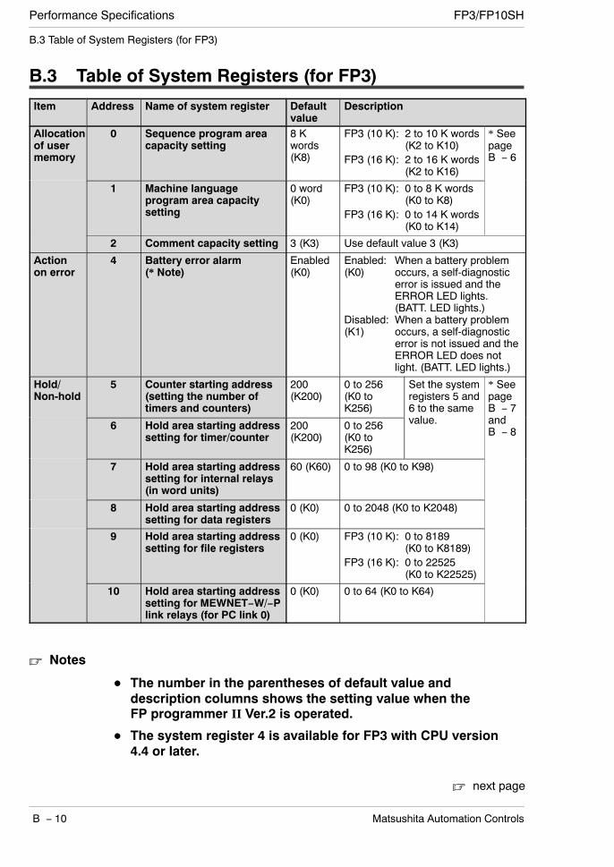
Performance Specifications FP3/FP10SH
B − 10 Matsushita Automation Controls
B.3 Table of System Registers (for FP3)
B.3 Table of System Registers (for FP3)
Item Address Name of system register Defaultvalue
Description
Allocationof usermemory
0 Sequence program areacapacity setting
8 Kwords(K8)
FP3 (10 K): 2 to 10 K words(K2 to K10)
FP3 (16 K): 2 to 16 K words(K2 to K16)
* SeepageB − 6
1 Machine languageprogram area capacitysetting
0 word(K0)
FP3 (10 K): 0 to 8 K words(K0 to K8)
FP3 (16 K): 0 to 14 K words(K0 to K14)
2 Comment capacity setting 3 (K3) Use default value 3 (K3)
Actionon error
4 Battery error alarm(* Note)
Enabled(K0)
Enabled: When a battery problem(K0) occurs, a self-diagnostic
error is issued and theERROR LED lights.(BATT. LED lights.)
Disabled: When a battery problem(K1) occurs, a self-diagnostic
error is not issued and theERROR LED does notlight. (BATT. LED lights.)
Hold/Non-hold
5 Counter starting address(setting the number oftimers and counters)
200(K200)
0 to 256(K0 toK256)
Set the systemregisters 5 and6 to the samel
* SeepageB − 7d6 Hold area starting address
setting for timer/counter200(K200)
0 to 256(K0 toK256)
value. andB − 8
7 Hold area starting addresssetting for internal relays(in word units)
60 (K60) 0 to 98 (K0 to K98)
8 Hold area starting addresssetting for data registers
0 (K0) 0 to 2048 (K0 to K2048)
9 Hold area starting addresssetting for file registers
0 (K0) FP3 (10 K): 0 to 8189(K0 to K8189)
FP3 (16 K): 0 to 22525(K0 to K22525)
10 Hold area starting addresssetting for MEWNET−W/−Plink relays (for PC link 0)
0 (K0) 0 to 64 (K0 to K64)
Notes
The number in the parentheses of default value anddescription columns shows the setting value when theFP programmer II Ver.2 is operated.
The system register 4 is available for FP3 with CPU version4.4 or later.
next page
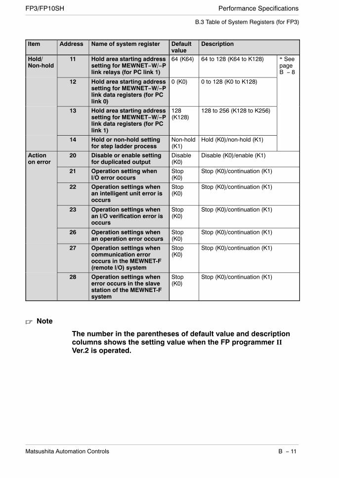
Performance SpecificationsFP3/FP10SH
B − 11Matsushita Automation Controls
B.3 Table of System Registers (for FP3)
Item Address Name of system register Defaultvalue
Description
Hold/Non-hold
11 Hold area starting addresssetting for MEWNET−W/−Plink relays (for PC link 1)
64 (K64) 64 to 128 (K64 to K128) * SeepageB − 8
12 Hold area starting addresssetting for MEWNET−W/−Plink data registers (for PClink 0)
0 (K0) 0 to 128 (K0 to K128)
13 Hold area starting addresssetting for MEWNET−W/−Plink data registers (for PClink 1)
128(K128)
128 to 256 (K128 to K256)
14 Hold or non-hold settingfor step ladder process
Non-hold(K1)
Hold (K0)/non-hold (K1)
Actionon error
20 Disable or enable settingfor duplicated output
Disable(K0)
Disable (K0)/enable (K1)
21 Operation setting whenI/O error occurs
Stop(K0)
Stop (K0)/continuation (K1)
22 Operation settings whenan intelligent unit error isoccurs
Stop(K0)
Stop (K0)/continuation (K1)
23 Operation settings whenan I/O verification error isoccurs
Stop(K0)
Stop (K0)/continuation (K1)
26 Operation settings whenan operation error occurs
Stop(K0)
Stop (K0)/continuation (K1)
27 Operation settings whencommunication erroroccurs in the MEWNET-F(remote I/O) system
Stop(K0)
Stop (K0)/continuation (K1)
28 Operation settings whenerror occurs in the slavestation of the MEWNET-Fsystem
Stop(K0)
Stop (K0)/continuation (K1)
Note
The number in the parentheses of default value and descriptioncolumns shows the setting value when the FP programmer IIVer.2 is operated.
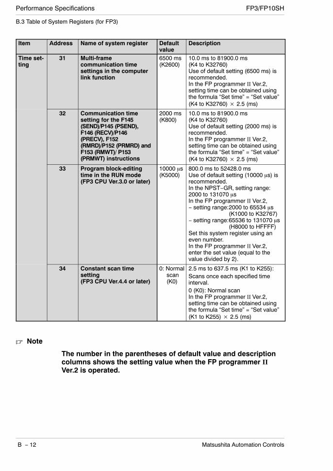
Performance Specifications FP3/FP10SH
B − 12 Matsushita Automation Controls
B.3 Table of System Registers (for FP3)
Item Address Name of system register Defaultvalue
Description
Time set-ting
31 Multi-framecommunication timesettings in the computerlink function
6500 ms(K2600)
10.0 ms to 81900.0 ms(K4 to K32760)Use of default setting (6500 ms) isrecommended.In the FP programmer II Ver.2,setting time can be obtained usingthe formula “Set time” = “Set value”(K4 to K32760)× 2.5 (ms)
32 Communication timesetting for the F145(SEND)/P145 (PSEND),F146 (RECV)/P146(PRECV), F152(RMRD)/P152 (PRMRD) andF153 (RMWT)/ P153(PRMWT) instructions
2000 ms(K800)
10.0 ms to 81900.0 ms(K4 to K32760)Use of default setting (2000 ms) isrecommended.In the FP programmer II Ver.2,setting time can be obtained usingthe formula “Set time” = “Set value”(K4 to K32760)× 2.5 (ms)
33 Program block-editingtime in the RUN mode(FP3 CPU Ver.3.0 or later)
10000 μs(K5000)
800.0 ms to 52428.0 msUse of default setting (10000 μs) isrecommended.In the NPST−GR, setting range:2000 to 131070 μsIn the FP programmer II Ver.2,− setting range:2000 to 65534 μs
(K1000 to K32767)− setting range:65536 to 131070 μs
(H8000 to HFFFF)Set this system register using aneven number.In the FP programmer II Ver.2,enter the set value (equal to thevalue divided by 2).
34 Constant scan timesetting(FP3 CPU Ver.4.4 or later)
0: Normalscan(K0)
2.5 ms to 637.5 ms (K1 to K255):Scans once each specified timeinterval.0 (K0): Normal scanIn the FP programmer II Ver.2,setting time can be obtained usingthe formula “Set time” = “Set value”(K1 to K255)× 2.5 (ms)
Note
The number in the parentheses of default value and descriptioncolumns shows the setting value when the FP programmer IIVer.2 is operated.
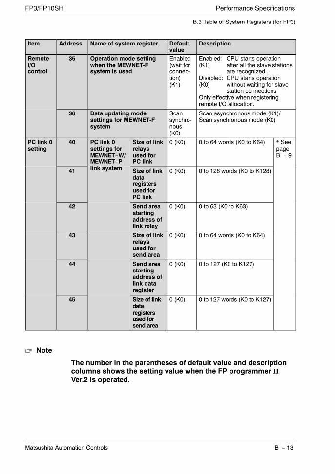
Performance SpecificationsFP3/FP10SH
B − 13Matsushita Automation Controls
B.3 Table of System Registers (for FP3)
Item Address Name of system register Defaultvalue
Description
RemoteI/Ocontrol
35 Operation mode settingwhen the MEWNET-Fsystem is used
Enabled(wait forconnec-tion)(K1)
Enabled: CPU starts operation(K1) after all the slave stations
are recognized.Disabled: CPU starts operation(K0) without waiting for slave
station connectionsOnly effective when registeringremote I/O allocation.
36 Data updating modesettings for MEWNET-Fsystem
Scansynchro-nous(K0)
Scan asynchronous mode (K1)/Scan synchronous mode (K0)
PC link 0setting
40 PC link 0settings forMEWNET−W/MEWNET−Pli k t
Size of linkrelaysused forPC link
0 (K0) 0 to 64 words (K0 to K64) * SeepageB − 9
41 link system Size of linkdataregistersused forPC link
0 (K0) 0 to 128 words (K0 to K128)
42 Send areastartingaddress oflink relay
0 (K0) 0 to 63 (K0 to K63)
43 Size of linkrelaysused forsend area
0 (K0) 0 to 64 words (K0 to K64)
44 Send areastartingaddress oflink dataregister
0 (K0) 0 to 127 (K0 to K127)
45 Size of linkdataregistersused forsend area
0 (K0) 0 to 127 words (K0 to K127)
Note
The number in the parentheses of default value and descriptioncolumns shows the setting value when the FP programmer IIVer.2 is operated.
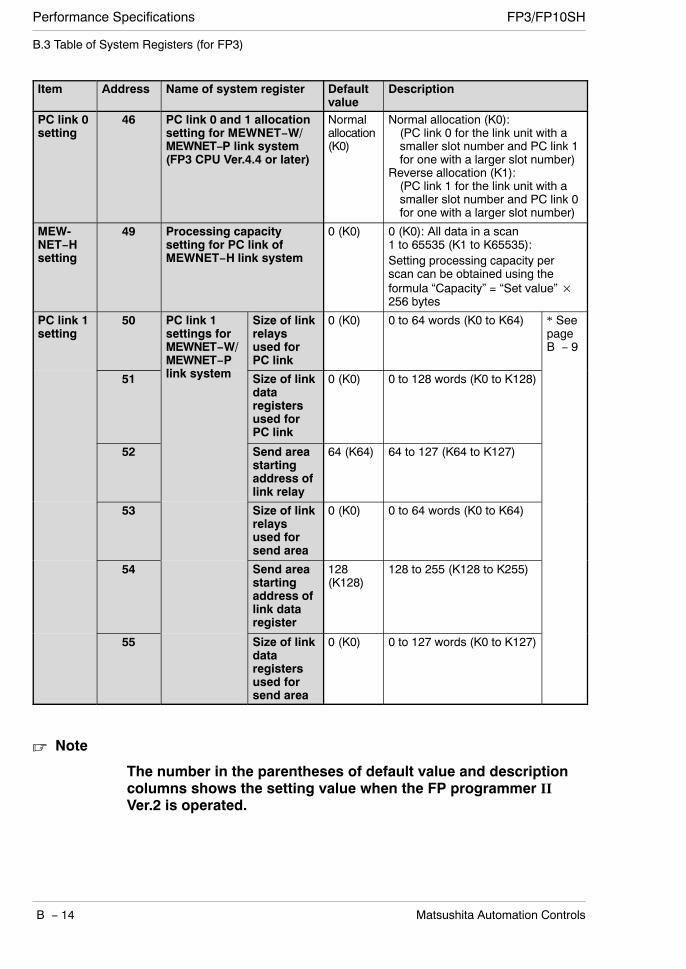
Performance Specifications FP3/FP10SH
B − 14 Matsushita Automation Controls
B.3 Table of System Registers (for FP3)
Item Address Name of system register Defaultvalue
Description
PC link 0setting
46 PC link 0 and 1 allocationsetting for MEWNET−W/MEWNET−P link system(FP3 CPU Ver.4.4 or later)
Normalallocation(K0)
Normal allocation (K0):(PC link 0 for the link unit with asmaller slot number and PC link 1for one with a larger slot number)
Reverse allocation (K1):(PC link 1 for the link unit with asmaller slot number and PC link 0for one with a larger slot number)
MEW-NET−Hsetting
49 Processing capacitysetting for PC link ofMEWNET−H link system
0 (K0) 0 (K0): All data in a scan1 to 65535 (K1 to K65535):Setting processing capacity perscan can be obtained using theformula “Capacity” = “Set value”×256 bytes
PC link 1setting
50 PC link 1settings forMEWNET−W/MEWNET−Pli k t
Size of linkrelaysused forPC link
0 (K0) 0 to 64 words (K0 to K64) * SeepageB − 9
51 link system Size of linkdataregistersused forPC link
0 (K0) 0 to 128 words (K0 to K128)
52 Send areastartingaddress oflink relay
64 (K64) 64 to 127 (K64 to K127)
53 Size of linkrelaysused forsend area
0 (K0) 0 to 64 words (K0 to K64)
54 Send areastartingaddress oflink dataregister
128(K128)
128 to 255 (K128 to K255)
55 Size of linkdataregistersused forsend area
0 (K0) 0 to 127 words (K0 to K127)
Note
The number in the parentheses of default value and descriptioncolumns shows the setting value when the FP programmer IIVer.2 is operated.
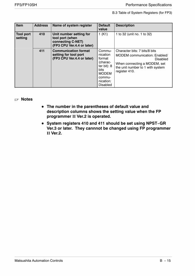
Performance SpecificationsFP3/FP10SH
B − 15Matsushita Automation Controls
B.3 Table of System Registers (for FP3)
Item Address Name of system register Defaultvalue
Description
Tool portsetting
410 Unit number setting fortool port (whenconnecting C-NET)(FP3 CPU Ver.4.4 or later)
1 (K1) 1 to 32 (unit no. 1 to 32)
411 Communication formatsetting for tool port(FP3 CPU Ver.4.4 or later)
Commu-nicationformat(charac-ter bit): 8bitsMODEMcommu-nication:Disabled
Character bits: 7 bits/8 bitsMODEM communication: Enabled/
DisabledWhen connecting a MODEM, setthe unit number to 1 with systemregister 410.
Notes
The number in the parentheses of default value anddescription columns shows the setting value when the FPprogrammer II Ver.2 is operated.
System registers 410 and 411 should be set using NPST−GRVer.3 or later. They cannnot be changed using FP programmerII Ver.2.

Performance Specifications FP3/FP10SH
B − 16 Matsushita Automation Controls
B.4 Table of System Registers (for FP10SH)
B.4 Table of System Registers (for FP10SH)
Item Address Name of system register Defaultvalue
Description
Actionon error
4 Battery error alarm Enabled Enabled: When a battery problemoccurs, a self-diagnosticerror is issued and theERROR LED lights.
Disabled: When a battery problemoccurs, a self-diagnosticerror is not issued and theERROR LED does notlight. (BATT. LED lights.)
Memory areacontentstti t
Internalrelay (R)
Cleared Cleared: When the initialize/test switch is set toINITIALIZE itisetting at
INITIALIZEposition
Link relay(L)
Cleared INITIALIZE positionwhile in the PROG.mode you canposition
Timers/Counters(T, C, SV,EV)
Clearedmode, you canspecify the type ofmemory to becleared.
Not cleared: When the initialize/Dataregister(DT)
ClearedNot cleared: When the initialize/
test switch is set toINITIALIZE positionwhile in the PROG.mode o canLink data
register(LD)
Cleared mode, you canspecify the type ofmemory to be notcleared.
Fileregister(FL)
Clearedcleared.
Indexregister (I)
Cleared
Error alarmrelay (E)
Cleared
Differential typeinstructions settingbetween MC and MCEinstructions
0(conven-tional)
0 (conventional): Holds precededresult in the MC and MCEinstruction set1 (new): Disregards preceded resultin the MC and MCE instruction set(See section B.4.1)
TM instruction operationsetting
0(conven-tional)
0 (conventional): Scan synchronous1 (new): Scan asynchronous
Index modifier checksetting
Enabled Enabled: Checks for overflow of theindex modifier area, andperforms normalprocessing.
Disabled: Performs processingwithout checking foroverflow of the indexmodifier area.
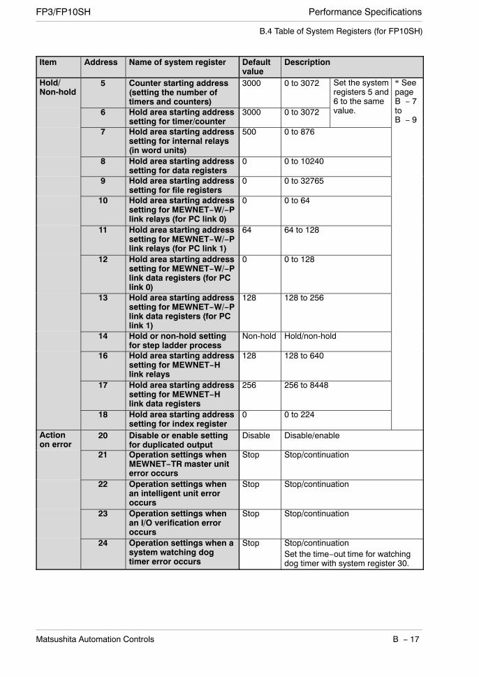
Performance SpecificationsFP3/FP10SH
B − 17Matsushita Automation Controls
B.4 Table of System Registers (for FP10SH)
Item Address Name of system register Defaultvalue
Description
Hold/Non-hold
5 Counter starting address(setting the number oftimers and counters)
3000 0 to 3072 Set the systemregisters 5 and6 to the samel
* SeepageB − 7
6 Hold area starting addresssetting for timer/counter
3000 0 to 3072 value. toB − 9
7 Hold area starting addresssetting for internal relays(in word units)
500 0 to 876
8 Hold area starting addresssetting for data registers
0 0 to 10240
9 Hold area starting addresssetting for file registers
0 0 to 32765
10 Hold area starting addresssetting for MEWNET−W/−Plink relays (for PC link 0)
0 0 to 64
11 Hold area starting addresssetting for MEWNET−W/−Plink relays (for PC link 1)
64 64 to 128
12 Hold area starting addresssetting for MEWNET−W/−Plink data registers (for PClink 0)
0 0 to 128
13 Hold area starting addresssetting for MEWNET−W/−Plink data registers (for PClink 1)
128 128 to 256
14 Hold or non-hold settingfor step ladder process
Non-hold Hold/non-hold
16 Hold area starting addresssetting for MEWNET−Hlink relays
128 128 to 640
17 Hold area starting addresssetting for MEWNET−Hlink data registers
256 256 to 8448
18 Hold area starting addresssetting for index register
0 0 to 224
Actionon error
20 Disable or enable settingfor duplicated output
Disable Disable/enableon error
21 Operation settings whenMEWNET−TR master uniterror occurs
Stop Stop/continuation
22 Operation settings whenan intelligent unit erroroccurs
Stop Stop/continuation
23 Operation settings whenan I/O verification erroroccurs
Stop Stop/continuation
24 Operation settings when asystem watching dogtimer error occurs
Stop Stop/continuationSet the time−out time for watchingdog timer with system register 30.

Performance Specifications FP3/FP10SH
B − 18 Matsushita Automation Controls
B.4 Table of System Registers (for FP10SH)
Item Address Name of system register Defaultvalue
Description
Actionon error
26 Operation settings whenan operation error occurs
Stop Stop/continuation
27 Operation settings whencommunication erroroccurs in the MEWNET-F(remote I/O) system
Stop Stop/continuation
28 Operation settings whenerror occurs in the slavestation of the MEWNET-Fsystem
Stop Stop/continuation
Timesetting
29 Operation time setting forperipheral tasks
300(240 μs)
0 to 65535 (0 to 52428 μs)The setting for this system registeris effective in the RUN mode only.In the PROG. mode and “0” setting,the allowable duration of time usedfor peripheral tasks is set at52428 μs.Setting time can be obtained usingthe formula“Set time” = “Set value”× 0.8 (μs)
30 Time−out time setting ofsystem watching dogtimer
1000(100 ms)
4 to 6400 (0.4 to 640 ms)Setting time can be obtained usingthe formula“Set time” =“Set value”× 0.1 (ms)
31 Multi-framecommunication timesettings in the computerlink function andcommunication timesetting for data sendingbuffer
2600(6.5 s)
4 to 32767 (0.01 to 81.9175 s)Use of default setting (6.5 s) isrecommended.Setting time can be obtained usingthe formula“Set time” =“Set value”× 2.5 (ms)
32 Communication timesetting for the F145(SEND)/P145 (PSEND),F146 (RECV)/P146(PRECV), F152(RMRD)/P152 (PRMRD) andF153 (RMWT)/ P153(PRMWT) instructions
4000(10 s)
4 to 32767 (0.01 to 81.9175 s)Use of default setting (10 s) isrecommended.Setting time can be obtained usingthe formula“Set time” =“Set value”× 2.5 (ms)
33 Effective time setting formonitoring
65535(163.8375 s)
1000 to 65535 ( 2.5 to 163.8375 s)Use of default setting (163.8375 s)is recommended.Setting time can be obtained usingthe formula“Set time” =“Set value”× 2.5 (ms)
34 Constant scan timesetting
0: Normalscan
1 to 64000 (0.1 to 6400 ms):Scans once each specified timeinterval.0: Normal scanSetting time can be obtained usingthe formula“Set time” =“Set value”× 0.1 (ms)
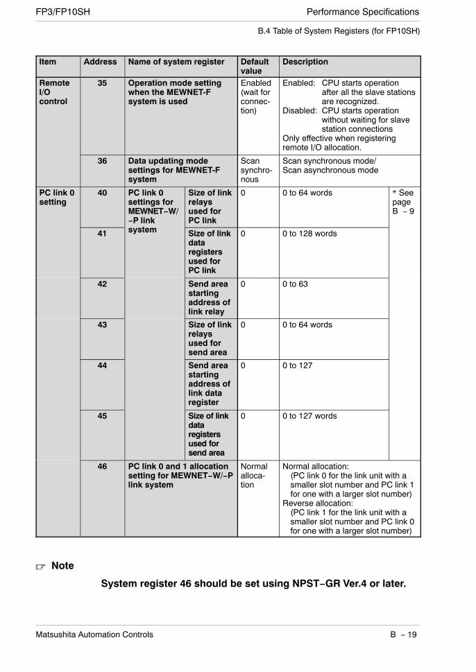
Performance SpecificationsFP3/FP10SH
B − 19Matsushita Automation Controls
B.4 Table of System Registers (for FP10SH)
Item Address Name of system register Defaultvalue
Description
RemoteI/Ocontrol
35 Operation mode settingwhen the MEWNET-Fsystem is used
Enabled(wait forconnec-tion)
Enabled: CPU starts operationafter all the slave stationsare recognized.
Disabled: CPU starts operationwithout waiting for slavestation connections
Only effective when registeringremote I/O allocation.
36 Data updating modesettings for MEWNET-Fsystem
Scansynchro-nous
Scan synchronous mode/Scan asynchronous mode
PC link 0setting
40 PC link 0settings forMEWNET−W/−P link
t
Size of linkrelaysused forPC link
0 0 to 64 words * SeepageB − 9
41 system Size of linkdataregistersused forPC link
0 0 to 128 words
42 Send areastartingaddress oflink relay
0 0 to 63
43 Size of linkrelaysused forsend area
0 0 to 64 words
44 Send areastartingaddress oflink dataregister
0 0 to 127
45 Size of linkdataregistersused forsend area
0 0 to 127 words
46 PC link 0 and 1 allocationsetting for MEWNET−W/−Plink system
Normalalloca-tion
Normal allocation:(PC link 0 for the link unit with asmaller slot number and PC link 1for one with a larger slot number)
Reverse allocation:(PC link 1 for the link unit with asmaller slot number and PC link 0for one with a larger slot number)
Note
System register 46 should be set using NPST−GR Ver.4 or later.
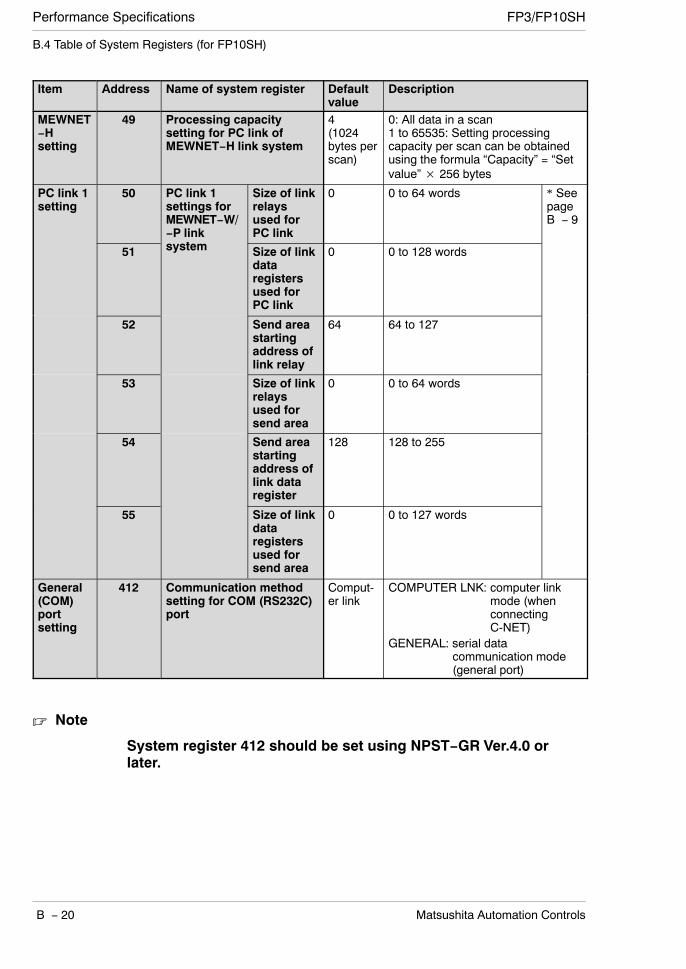
Performance Specifications FP3/FP10SH
B − 20 Matsushita Automation Controls
B.4 Table of System Registers (for FP10SH)
Item Address Name of system register Defaultvalue
Description
MEWNET−Hsetting
49 Processing capacitysetting for PC link ofMEWNET−H link system
4(1024bytes perscan)
0: All data in a scan1 to 65535: Setting processingcapacity per scan can be obtainedusing the formula “Capacity” = “Setvalue”× 256 bytes
PC link 1setting
50 PC link 1settings forMEWNET−W/−P link
t
Size of linkrelaysused forPC link
0 0 to 64 words * SeepageB − 9
51 system Size of linkdataregistersused forPC link
0 0 to 128 words
52 Send areastartingaddress oflink relay
64 64 to 127
53 Size of linkrelaysused forsend area
0 0 to 64 words
54 Send areastartingaddress oflink dataregister
128 128 to 255
55 Size of linkdataregistersused forsend area
0 0 to 127 words
General(COM)portsetting
412 Communication methodsetting for COM (RS232C)port
Comput-er link
COMPUTER LNK: computer linkmode (whenconnectingC-NET)
GENERAL: serial datacommunication mode(general port)
Note
System register 412 should be set using NPST−GR Ver.4.0 orlater.
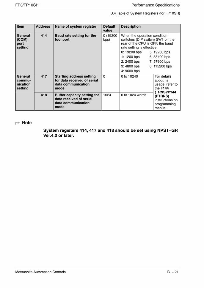
Performance SpecificationsFP3/FP10SH
B − 21Matsushita Automation Controls
B.4 Table of System Registers (for FP10SH)
Item Address Name of system register Defaultvalue
Description
General(COM)portsetting
414 Baud rate setting for thetool port
0 (19200bps)
When the operation conditionswitches (DIP switch) SW1 on therear of the CPU is OFF, the baudrate setting is effective.0: 19200 bps 5: 19200 bps1: 1200 bps 6: 38400 bps2: 2400 bps 7: 57600 bps3: 4800 bps 8: 115200 bps4: 9600 bps
Generalcommu-nicationsetting
417 Starting address settingfor data received of serialdata communicationmode
0 0 to 10240 For detailsabout itsusage, refer tothe F144(TRNS)/P144
418 Buffer capacity setting fordata received of serialdata communicationmode
1024 0 to 1024 words(TRNS)/P144(PTRNS)instructions onprogrammingmanual.
Note
System registers 414, 417 and 418 should be set using NPST−GRVer.4.0 or later.
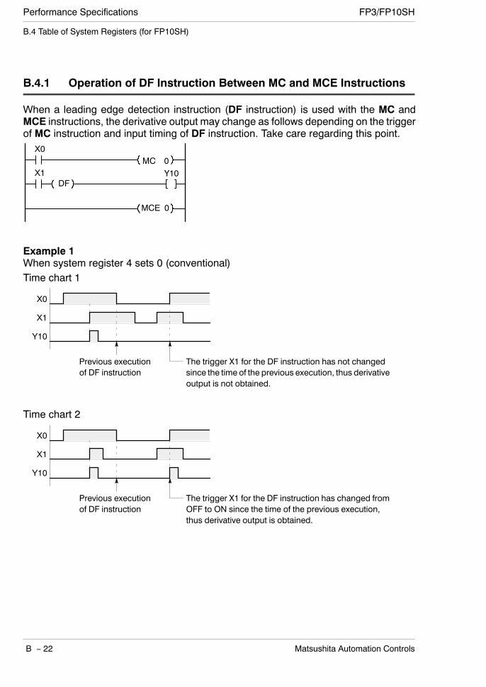
Performance Specifications FP3/FP10SH
B − 22 Matsushita Automation Controls
B.4 Table of System Registers (for FP10SH)
B.4.1 Operation of DF Instruction Between MC and MCE Instructions
When a leading edge detection instruction (DF instruction) is used with the MC andMCE instructions, the derivative output may change as follows depending on the triggerof MC instruction and input timing of DF instruction. Take care regarding this point.
X1DF
Y10
MCE 0
X0MC 0
Example 1When system register 4 sets 0 (conventional)Time chart 1
X0
X1
Y10
Previous executionof DF instruction
The trigger X1 for the DF instruction has not changedsince the time of the previous execution, thus derivativeoutput is not obtained.
Time chart 2
X0
X1
Y10
Previous executionof DF instruction
The trigger X1 for the DF instruction has changed fromOFF to ON since the time of the previous execution,thus derivative output is obtained.
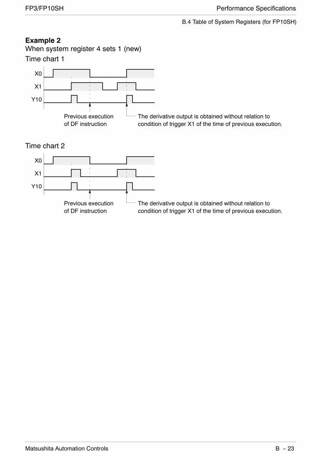
Performance SpecificationsFP3/FP10SH
B − 23Matsushita Automation Controls
B.4 Table of System Registers (for FP10SH)
Example 2When system register 4 sets 1 (new)Time chart 1
X0
X1
Y10
Previous executionof DF instruction
The derivative output is obtained without relation tocondition of trigger X1 of the time of previous execution.
Time chart 2
X0
X1
Y10
Previous executionof DF instruction
The derivative output is obtained without relation tocondition of trigger X1 of the time of previous execution.

Performance Specifications FP3/FP10SH
B − 24 Matsushita Automation Controls
B.4 Table of System Registers (for FP10SH)
Appendix C
Table of Relays, Memory Areas andConstants
C.1 Relays, Memory Areas and Constantsfor FP3 C − 3. . . . . . . . . . . . . . . . . . . . . . . . . . . . . . . .
C.2 Relays, Memory Areas and Constantsfor FP10SH C − 6. . . . . . . . . . . . . . . . . . . . . . . . . . . .
C.3 Relay Numbers C − 9. . . . . . . . . . . . . . . . . . . . . . . . .

Performance Specifications FP3/FP10SH
C − 2 Matsushita Automation Controls
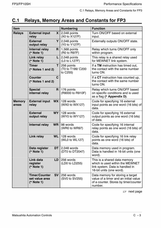
Performance SpecificationsFP3/FP10SH
C − 3Matsushita Automation Controls
C.1 Relays, Memory Areas and Constants for FP3
C.1 Relays, Memory Areas and Constants for FP3
Item Numbering FunctionRelays External input
relayX 2,048 points
(X0 to X127F)Turn ON/OFF based on externalinput.
Externaloutput relay
Y 2,048 points(Y0 to Y127F)
Externally outputs ON/OFF state.
Internal relay(* Note 1)
R 1,568 points(R0 to R97F)
Relay which turns ON/OFF onlywithin program.
Link relay(* Note 1)
L 2,048 points(L0 to L127F)
This relay is a shared relay usedfor MEWNET link system.
Timer T 256 points(T T / C
If a TM instruction has timed out,h i h h b(* Notes 1 and 2)
p(T0 to T199/ C200to C255)
,the contact with the same numberturns ON.
Counter C If a CT instruction has counted up,h i h h b(* Notes 1 and 2)
p,the contact with the same numberturns ON.
Specialinternal relay
R 176 points(R9000 to R910F)
Relay which turns ON/OFF basedon specific conditions and is usedas a flag (* Appendix D).
Memoryareas
External inputrelay
WX 128 words(WX0 to WX127)
Code for specifying 16 externalinput points as one word (16 bits) ofdata.
Externaloutput relay
WY 128 words(WY0 to WY127)
Code for specifying 16 externaloutput points as one word (16 bits)of data.
Internal relay WR 98 words(WR0 to WR97)
Code for specifying 16 internalrelay points as one word (16 bits) ofdata.
Link relay WL 128 words(WL0 to WL127)
Code for specifying 16 link relaypoints as one word (16 bits) ofdata.
Data register(* Note 1)
DT 2,048 words(DT0 to DT2047)
Data memory used in program.Data is handled in 16-bit units (oneword).
Link dataregister(* Note 1)
LD 256 words(LD0 to LD255)
This is a shared data memorywhich is used within the MEWNETlink system. Data is handled in16-bit units (one word).
Timer/Counterset value area(* Note 1)
SV 256 words(SV0 to SV255)
Data memory for storing a targetvalue of a timer and an initial valueof a counter. Stores by timer/counternumber.
next page
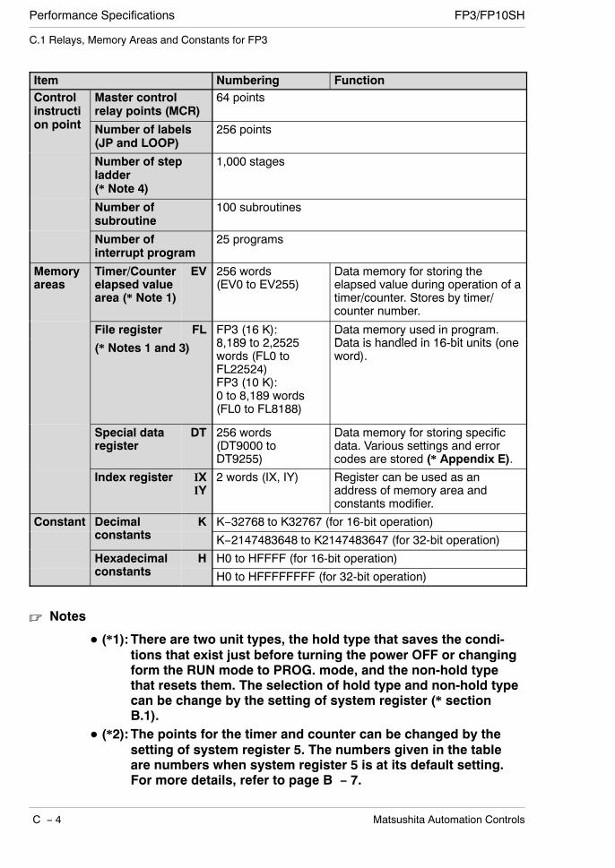
Performance Specifications FP3/FP10SH
C − 4 Matsushita Automation Controls
C.1 Relays, Memory Areas and Constants for FP3
Item Numbering FunctionControlinstructi
i t
Master controlrelay points (MCR)
64 points
on point Number of labels(JP and LOOP)
256 points
Number of stepladder(* Note 4)
1,000 stages
Number ofsubroutine
100 subroutines
Number ofinterrupt program
25 programs
Memoryareas
Timer/Counterelapsed valuearea (* Note 1)
EV 256 words(EV0 to EV255)
Data memory for storing theelapsed value during operation of atimer/counter. Stores by timer/counter number.
File register FL FP3 (16 K):8 189 t 2 2525
Data memory used in program.D t i h dl d i 16 bit it ((* Notes 1 and 3)
( )8,189 to 2,2525words (FL0 toFL22524)FP3 (10 K):0 to 8,189 words(FL0 to FL8188)
y p gData is handled in 16-bit units (oneword).
Special dataregister
DT 256 words(DT9000 toDT9255)
Data memory for storing specificdata. Various settings and errorcodes are stored (* Appendix E).
Index register IXIY
2 words (IX, IY) Register can be used as anaddress of memory area andconstants modifier.
Constant Decimalt t
K K−32768 to K32767 (for 16-bit operation)constants K−2147483648 to K2147483647 (for 32-bit operation)
Hexadecimalt t
H H0 to HFFFF (for 16-bit operation)constants H0 to HFFFFFFFF (for 32-bit operation)
Notes
(*1):There are two unit types, the hold type that saves the condi-tions that exist just before turning the power OFF or changingform the RUN mode to PROG. mode, and the non-hold typethat resets them. The selection of hold type and non-hold typecan be change by the setting of system register (* sectionB.1).
(*2):The points for the timer and counter can be changed by thesetting of system register 5. The numbers given in the tableare numbers when system register 5 is at its default setting.For more details, refer to page B − 7.

Performance SpecificationsFP3/FP10SH
C − 5Matsushita Automation Controls
(*3):The size of the file register varies depending on the settings ofsystem registers 0 and 1. For details, refer to page B − 6.
(*4):Hold or non-hold type can be set.
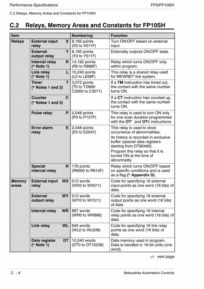
Performance Specifications FP3/FP10SH
C − 6 Matsushita Automation Controls
C.2 Relays, Memory Areas and Constants for FP10SH
C.2 Relays, Memory Areas and Constants for FP10SH
Item Numbering FunctionRelays External input
relayX 8,192 points
(X0 to X511F)Turn ON/OFF based on externalinput.
Externaloutput relay
Y 8,192 points(Y0 to Y511F)
Externally outputs ON/OFF state.
Internal relay(* Note 1)
R 14,192 points(R0 to R886F)
Relay which turns ON/OFF onlywithin program.
Link relay(* Note 1)
L 10,240 points(L0 to L639F)
This relay is a shared relay usedfor MEWNET link system.
Timer T 3,072 points(T T /
If a TM instruction has timed out,h i h h b(* Notes 1 and 2)
, p(T0 to T2999/C3000 to C3071)
,the contact with the same numberturns ON.
Counter C If a CT instruction has counted up,h i h h b(* Notes 1 and 2)
p,the contact with the same numberturns ON.
Pulse relay P 2,048 points(P0 to P127F)
This relay is used to turn ON onlyfor one scan duration programmedwith the OT" and OT# instructions.
Error alarmrelay
E 2,048 points(E0 to E2047)
This relay is used to storeoccurrence of abnormalities.Its history is recorded in exclusivebuffer (special data registersstarting from DT90400).Program this relay so that it isturned ON at the time ofabnormality.
Specialinternal relay
R 176 points(R9000 to R910F)
Relay which turns ON/OFF basedon specific conditions and is usedas a flag (* Appendix D).
Memoryareas
External inputrelay
WX 512 words(WX0 to WX511)
Code for specifying 16 externalinput points as one word (16 bits) ofdata.
Externaloutput relay
WY 512 words(WY0 to WY511)
Code for specifying 16 externaloutput points as one word (16 bits)of data.
Internal relay WR 887 words(WR0 to WR886)
Code for specifying 16 internalrelay points as one word (16 bits) ofdata.
Link relay WL 640 words(WL0 to WL639)
Code for specifying 16 link relaypoints as one word (16 bits) ofdata.
Data register(* Note 1)
DT 10,240 words(DT0 to DT10239)
Data memory used in program.Data is handled in 16-bit units (oneword).
next page

Performance SpecificationsFP3/FP10SH
C − 7Matsushita Automation Controls
C.2 Relays, Memory Areas and Constants for FP10SH
Item Numbering FunctionMemoryareas
Link dataregister(* Note 1)
LD 8,448 words(LD0 to LD8447)
This is a shared data memory which isused within the MEWNET link system.Data is handled in 16-bit units (oneword).
Timer/Counterset value area(* Note 1)
SV 3,072 words(SV0 to SV3071)
Data memory for storing a target valueof a timer and an initial value of acounter. Stores by timer/counter number.
Timer/Counterelapsed valuearea (* Note 1)
EV 3,072 words(EV0 to EV3071)
Data memory for storing the elapsedvalue during operation of atimer/counter. Stores by timer/ counternumber.
File register FL 32,765 words(FL0 t FL32764)
Data memory used in program. Data ish dl d i 16 bit it ( d)(* Note 1) (FL0 to FL32764)
y p ghandled in 16-bit units (one word).
Special dataregister
DT 512 words(DT90000 toDT90511)
Data memory for storing specific data.Various settings and error codes arestored (* Appendix E).
Index register I 14 words×16banks (I0 to ID)
Register can be used as an address ofmemory area and constants modifier.
Controlinstruc-tion
i t
Master controlrelay points (MCR)
256 points (when using the 90k step expansion memory,up to a total of 512 points can be used for the 1st and 2ndprograms)
point Number of labels(JP and LOOP)
256 points (when using the 90k step expansion memory,up to a total of 512 points can be used for the 1st and 2ndprograms)
Number of stepladder (* Note 3)
1,000 steps (can only be used for the 1st program)
Number ofsubroutine
100 subroutines (can only be used for the 1st program)
Number ofinterrupt program
25 program (can only be used for the 1st program)
Constant Decimalconstants
K K−32768 to K32767 (for 16-bit operation)constants(integer type) K−2147483648 to K2147483647 (for 32-bit operation)
Hexadecimalt t
H H0 to HFFFF (for 16-bit operation)constants H0 to HFFFFFFFF (for 32-bit operation)
Decimalconstants(monorefinedreal number)
f f1.175494×10−38 to f3.402823×1038
Notes
(*1):There are two unit types, the hold type that saves the conditionsthat exist just before turning the power OFF or changing form theRUN mode to PROG. mode, and the non-hold type that resets

Performance Specifications FP3/FP10SH
C − 8 Matsushita Automation Controls
them. The selection of hold type and non-hold type can bechange by the setting of system register (* section B.1).
(*2):The points for the timer and counter can be changed by thesetting of system register 5. The numbers given in the tableare numbers when system register 5 is at its default setting.For more details, refer to page B − 7.
(*3):Hold or non-hold type can be set.
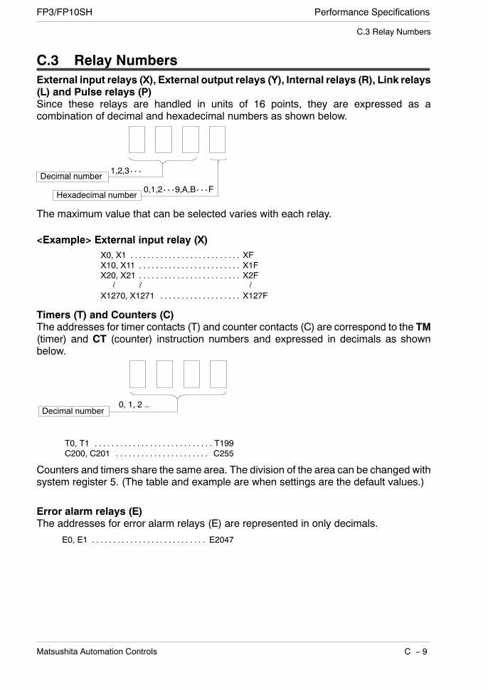
Performance SpecificationsFP3/FP10SH
C − 9Matsushita Automation Controls
C.3 Relay Numbers
C.3 Relay NumbersExternal input relays (X), External output relays (Y), Internal relays (R), Link relays(L) and Pulse relays (P)Since these relays are handled in units of 16 points, they are expressed as acombination of decimal and hexadecimal numbers as shown below.
1,2,3・・・Decimal number
0,1,2・・・9,A,B・・・FHexadecimal number
The maximum value that can be selected varies with each relay.
X0, X1 XF. . . . . . . . . . . . . . . . . . . . . . . . . .X10, X11 X1F. . . . . . . . . . . . . . . . . . . . . . . .X20, X21 X2F. . . . . . . . . . . . . . . . . . . . . . . .
X1270, X1271 X127F. . . . . . . . . . . . . . . . . . .
<Example> External input relay (X)
Timers (T) and Counters (C)The addresses for timer contacts (T) and counter contacts (C) are correspond to the TM(timer) and CT (counter) instruction numbers and expressed in decimals as shownbelow.
0, 1, 2…Decimal number
T0, T1 T199. . . . . . . . . . . . . . . . . . . . . . . . . . . .C200, C201 C255. . . . . . . . . . . . . . . . . . . . . .
Counters and timers share the same area. The division of the area can be changed withsystem register 5. (The table and example are when settings are the default values.)
Error alarm relays (E)The addresses for error alarm relays (E) are represented in only decimals.
E0, E1 E2047. . . . . . . . . . . . . . . . . . . . . . . . . . .
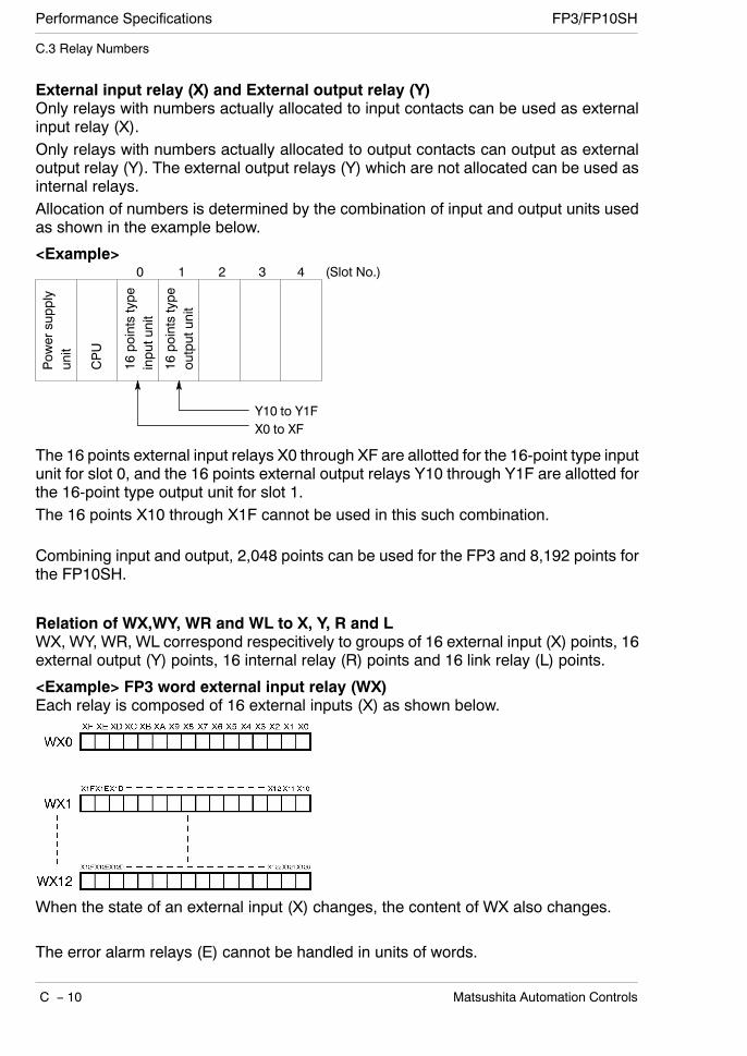
Performance Specifications FP3/FP10SH
C − 10 Matsushita Automation Controls
C.3 Relay Numbers
External input relay (X) and External output relay (Y)Only relays with numbers actually allocated to input contacts can be used as externalinput relay (X).Only relays with numbers actually allocated to output contacts can output as externaloutput relay (Y). The external output relays (Y) which are not allocated can be used asinternal relays.Allocation of numbers is determined by the combination of input and output units usedas shown in the example below.
<Example>0 1 2 3 4 (Slot No.)
Y10 to Y1FX0 to XF
Powersupply
unit
CPU
16pointstype
inputunit
16pointstype
outputunit
The 16 points external input relays X0 through XF are allotted for the 16-point type inputunit for slot 0, and the 16 points external output relays Y10 through Y1F are allotted forthe 16-point type output unit for slot 1.The 16 points X10 through X1F cannot be used in this such combination.
Combining input and output, 2,048 points can be used for the FP3 and 8,192 points forthe FP10SH.
Relation of WX,WY, WR and WL to X, Y, R and LWX, WY, WR, WL correspond respecitively to groups of 16 external input (X) points, 16external output (Y) points, 16 internal relay (R) points and 16 link relay (L) points.
<Example> FP3 word external input relay (WX)Each relay is composed of 16 external inputs (X) as shown below.
When the state of an external input (X) changes, the content of WX also changes.
The error alarm relays (E) cannot be handled in units of words.

Appendix D
Table of Special Internal Relays

Performance Specifications FP3/FP10SH
D − 2 Matsushita Automation Controls
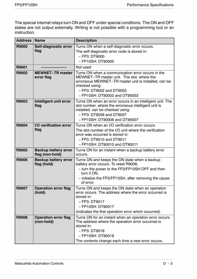
Performance SpecificationsFP3/FP10SH
D − 3Matsushita Automation Controls
The special internal relays turn ON and OFF under special conditions. The ON and OFFstates are not output externally. Writing is not possible with a programming tool or aninstruction.
Address Name Description
R9000 Self-diagnostic errorflag
Turns ON when a self-diagnostic error occurs.The self-diagnostic error code is stored in:− FP3: DT9000− FP10SH: DT90000
R9001 Not usedR9002 MEWNET−TR master
error flagTurns ON when a communication error occurs in theMEWNET−TR master unit. The slot, where theerroneous MEWNET−TR master unit is installed, can bechecked using:− FP3: DT9002 and DT9003− FP10SH: DT90002 and DT90003
R9003 Intelligent unit errorflag
Turns ON when an error occurs in an intelligent unit. Theslot number, where the erroneous intelligent unit isinstalled, can be checked using:− FP3: DT9006 and DT9007− FP10SH: DT90006 and DT90007
R9004 I/O verification errorflag
Turns ON when an I/O verification error occurs.The slot number of the I/O unit where the verificationerror was occurred is stored in:− FP3: DT9010 and DT9011− FP10SH: DT90010 and DT90011
R9005 Backup battery errorflag (non-hold)
Turns ON for an instant when a backup battery erroroccurs.
R9006 Backup battery errorflag (hold)
Turns ON and keeps the ON state when a backupbattery error occurs. To reset R9006,− turn the power to the FP3/FP10SH OFF and thenturn it ON,
− initialize the FP3/FP10SH, after removing the causeof error.
R9007 Operation error flag(hold)
Turns ON and keeps the ON state when an operationerror occurs. The address where the error occurred isstored in:− FP3: DT9017− FP10SH: DT90017
(indicates the first operation error which occurred).R9008 Operation error flag
(non-hold)Turns ON for an instant when an operation error occurs.The address where the operation error occurred isstored in:− FP3: DT9018− FP10SH: DT90018
The contents change each time a new error occurs.
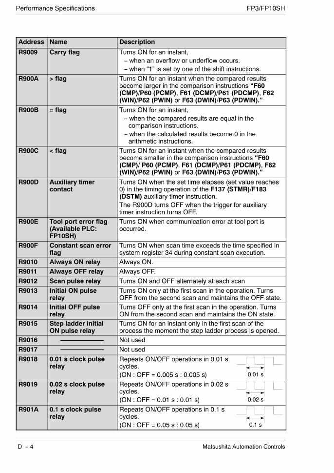
Performance Specifications FP3/FP10SH
D − 4 Matsushita Automation Controls
Address Name Description
R9009 Carry flag Turns ON for an instant,− when an overflow or underflow occurs.− when “1” is set by one of the shift instructions.
R900A > flag Turns ON for an instant when the compared resultsbecome larger in the comparison instructions “F60(CMP)/P60 (PCMP), F61 (DCMP)/P61 (PDCMP), F62(WIN)/P62 (PWIN) or F63 (DWIN)/P63 (PDWIN).”
R900B = flag Turns ON for an instant,− when the compared results are equal in thecomparison instructions.
− when the calculated results become 0 in thearithmetic instructions.
R900C < flag Turns ON for an instant when the compared resultsbecome smaller in the comparison instructions “F60(CMP)/ P60 (PCMP), F61 (DCMP)/P61 (PDCMP), F62(WIN)/P62 (PWIN) or F63 (DWIN)/P63 (PDWIN).”
R900D Auxiliary timercontact
Turns ON when the set time elapses (set value reaches0) in the timing operation of the F137 (STMR)/F183(DSTM) auxiliary timer instruction.The R900D turns OFF when the trigger for auxiliarytimer instruction turns OFF.
R900E Tool port error flag(Available PLC:FP10SH)
Turns ON when communication error at tool port isoccurred.
R900F Constant scan errorflag
Turns ON when scan time exceeds the time specified insystem register 34 during constant scan execution.
R9010 Always ON relay Always ON.R9011 Always OFF relay Always OFF.R9012 Scan pulse relay Turns ON and OFF alternately at each scanR9013 Initial ON pulse
relayTurns ON only at the first scan in the operation. TurnsOFF from the second scan and maintains the OFF state.
R9014 Initial OFF pulserelay
Turns OFF only at the first scan in the operation. TurnsON from the second scan and maintains the ON state.
R9015 Step ladder initialON pulse relay
Turns ON for an instant only in the first scan of theprocess the moment the step ladder process is opened.
R9016 Not usedR9017 Not usedR9018 0.01 s clock pulse
relayRepeats ON/OFF operations in 0.01 scycles.(ON : OFF = 0.005 s : 0.005 s) 0.01 s
R9019 0.02 s clock pulserelay
Repeats ON/OFF operations in 0.02 scycles.(ON : OFF = 0.01 s : 0.01 s) 0.02 s
R901A 0.1 s clock pulserelay
Repeats ON/OFF operations in 0.1 scycles.(ON : OFF = 0.05 s : 0.05 s) 0.1 s
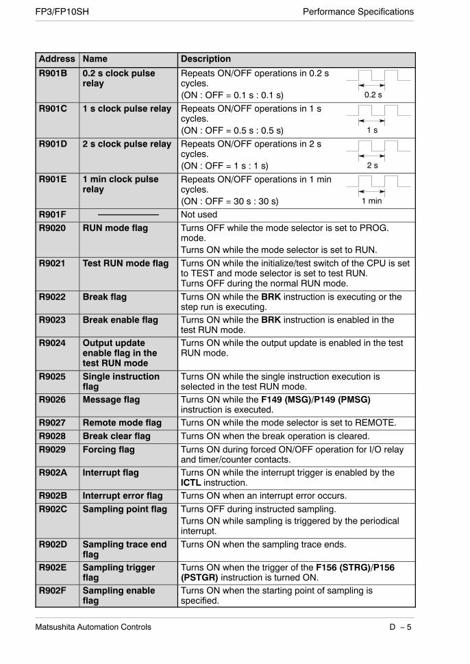
Performance SpecificationsFP3/FP10SH
D − 5Matsushita Automation Controls
Address Name Description
R901B 0.2 s clock pulserelay
Repeats ON/OFF operations in 0.2 scycles.(ON : OFF = 0.1 s : 0.1 s) 0.2 s
R901C 1 s clock pulse relay Repeats ON/OFF operations in 1 scycles.(ON : OFF = 0.5 s : 0.5 s) 1 s
R901D 2 s clock pulse relay Repeats ON/OFF operations in 2 scycles.(ON : OFF = 1 s : 1 s) 2 s
R901E 1 min clock pulserelay
Repeats ON/OFF operations in 1 mincycles.(ON : OFF = 30 s : 30 s) 1 min
R901F Not usedR9020 RUN mode flag Turns OFF while the mode selector is set to PROG.
mode.Turns ON while the mode selector is set to RUN.
R9021 Test RUN mode flag Turns ON while the initialize/test switch of the CPU is setto TEST and mode selector is set to test RUN.Turns OFF during the normal RUN mode.
R9022 Break flag Turns ON while the BRK instruction is executing or thestep run is executing.
R9023 Break enable flag Turns ON while the BRK instruction is enabled in thetest RUN mode.
R9024 Output updateenable flag in thetest RUN mode
Turns ON while the output update is enabled in the testRUN mode.
R9025 Single instructionflag
Turns ON while the single instruction execution isselected in the test RUN mode.
R9026 Message flag Turns ON while the F149 (MSG)/P149 (PMSG)instruction is executed.
R9027 Remote mode flag Turns ON while the mode selector is set to REMOTE.R9028 Break clear flag Turns ON when the break operation is cleared.R9029 Forcing flag Turns ON during forced ON/OFF operation for I/O relay
and timer/counter contacts.R902A Interrupt flag Turns ON while the interrupt trigger is enabled by the
ICTL instruction.R902B Interrupt error flag Turns ON when an interrupt error occurs.R902C Sampling point flag Turns OFF during instructed sampling.
Turns ON while sampling is triggered by the periodicalinterrupt.
R902D Sampling trace endflag
Turns ON when the sampling trace ends.
R902E Sampling triggerflag
Turns ON when the trigger of the F156 (STRG)/P156(PSTGR) instruction is turned ON.
R902F Sampling enableflag
Turns ON when the starting point of sampling isspecified.

Performance Specifications FP3/FP10SH
D − 6 Matsushita Automation Controls
Address Name Description
R9030 F145 (SEND)/P145(PSEND) and F146(RECV)/P146(PRECV) instructionexecuting flag
Monitors if FP3/FP10SH is in the F145 (SEND)/P145(PSEND) and F146 (RECV)/P146 (PRECV) instructionsexecutable condition as follows:− OFF: None of the above mentioned instructions can
be executed. (i.e., one of the aboveinstructions is being executed.)
− ON: One of the above mentioned instructions canbe executed.
R9031 F145 (SEND)/P145(PSEND) and F146(RECV)/P146(PRECV) instructionend flag
Monitors if an abnormality has been detected during theexecution of the F145 (SEND)/ P145 (PSEND) and F146(RECV)/P146 (PRECV) instructions as follows:− OFF: No abnormality detected.− ON: An abnormality detected. (communication
error)The error code is stored in:− FP3: DT9039− FP10SH: DT90039
R9032 COM port mode flag(Available PLC:FP10SH)
Monitors the mode of the COM port as:− ON: Serial data communication mode− OFF: Computer link mode
R9033 F147 (PR)instruction flag
Turns ON while a F147 (PR) instruction is executed.
R9034 Editing in RUNmode flag
Turns ON while editing a program in the RUN mode.
R9035 F152 (RMRD)/P152(PRMRD) and F153(RMWT)/P153(PRMWT)instructionexecution flag
Monitors if FP3/FP10SH is in the F152 (RMRD)/P152(PRMRD) and F153 (RMWT)/P153 (PRMWT)instructions executable condition as follows:− OFF: None of the above mentioned instructions can
be executed. (i.e., one of the aboveinstructions is being executed.)
− ON: One of the above mentioned instructions canbe executed.
R9036 F152 (RMRD)/P152(PRMRD) and F153(RMWT)/P153(PRMWT)instruction end flag
Monitors if an abnormality has been detected during theexecution of the F152 (RMRD)/P152 (PRMRD) andF153 (RMWT)/P153 (PRMWT) instructions as follows:− OFF: No abnormality detected.− ON: An abnormality detected. (access error)
The error code is stored in:− FP3: DT9036− FP10SH: DT90036
R9037 COM portcommunicationerror flag(Available PLC:FP10SH)
Turns ON when the serial data communication erroroccurs using COM port.Turns OFF when data is being sent by the F144 (TRNS)instruction.

Performance SpecificationsFP3/FP10SH
D − 7Matsushita Automation Controls
Address Name Description
R9038 COM port receiveflag(Available PLC:FP10SH)
Turns ON when a terminator is received during the serialdata communicating. (by the F144 (TRNS) instruction)
R9039 COM port send flag(Available PLC:FP10SH)
Turns ON while data is not send during the serial datacommunicating. (by the F144 (TRNS) instruction)Turns OFF while data is being sent during the serial datacommunicating. (by the F144 (TRNS) instruction)
R903A Not usedR903B Not usedR903C Not usedR903D Not usedR903E Not usedR903F Not usedR9050 MEWNET−W/−P link
transmission errorflag [W/P LINK 1]
When using MEWNET-W link unit or MEWNET−P link unit:− turns ON when transmission error occurs at link 1.− turns ON when there is an error in the link area settings.
R9051 MEWNET−W/−P linktransmission errorflag [W/P LINK 2]
When usingMEWNET-W link unit orMEWNET−P link unit:− turns ON when transmission error occurs at link 2.− turns ON when there is an error in the link area settings.
R9052 MEWNET−W/−P linktransmission errorflag [W/P LINK 3]
When usingMEWNET-W link unit orMEWNET−P link unit:− turns ON when transmission error occurs at link 3.− turns ON when there is an error in the link area settings.
R9053 MEWNET−W/−P linktransmission errorflag [W/P LINK 4](Available PLC:FP10SH)
When usingMEWNET-W link unit orMEWNET−P link unit:− turns ON when transmission error occurs at link 4.− turns ON when there is an error in the link area settings.
R9054 MEWNET−W/−P linktransmission errorflag [W/P LINK 5](Available PLC:FP10SH)
When using MEWNET-W link unit or MEWNET−P link unit:− turns ON when transmission error occurs at link 5.− turns ON when there is an error in the link area settings.
R9055 MEWNET−H linktransmission errorflag [H LINK 1](FP3 CPU Ver.4.3 orlater)
When using MEWNET−H link unit:− turns ON when trannsmission error occurs at H link 1.− turns ON when there is an error in the link area settings.
R9056 MEWNET−H linktransmission errorflag [H LINK 2](FP3 CPU Ver.4.3 orlater)
When using MEWNET−H link unit:− turns ON when trannsmission error occurs at H link 2.− turns ON when there is an error in the link area settings.
R9057 MEWNET−H linktransmission errorflag [H LINK 3](FP3 CPU Ver.4.3 orlater)
When using MEWNET−H link unit:− turns ON when trannsmission error occurs at H link 3.− turns ON when there is an error in the link area settings.

Performance Specifications FP3/FP10SH
D − 8 Matsushita Automation Controls
Address Name Description
R9058 Remote I/Otransmission errorflag (master 1)
When using remote I/O system (MEWNET-F):− turns ON when transmission error occurs on master 1.− turns ON when there is an error in the settings.
R9059 Remote I/Otransmission errorflag (master 2)
When using remote I/O system (MEWNET-F):− turns ON when transmission error occurs on master 2.− turns ON when there is an error in the settings.
R905A Remote I/Otransmission errorflag (master 3)
When using remote I/O system (MEWNET-F):− turns ON when transmission error occurs on master 3.− turns ON when there is an error in the settings.
R905B Remote I/Otransmission errorflag (master 4)
When using remote I/O system (MEWNET-F):− turns ON when transmission error occurs on master 4.− turns ON when there is an error in the settings.
R905C Not usedR905D Not usedR905E Not usedR905F Not used

Performance SpecificationsFP3/FP10SH
D − 9Matsushita Automation Controls
Address Name Description
R9060 MEWNET−W/−P PC linktransmissionassurancel [f PC
UnitNo.1
Turns ON when unit No. 1 is communicating properly inthe PC link mode.Turns OFF when operation is stopped, when an error isoccurring, or when not in the PC link mode.
R9061 relay [for PClink 0(W/P)]
UnitNo.2
Turns ON when unit No. 2 is communicating properly inthe PC link mode.Turns OFF when operation is stopped, when an error isoccurring, or when not in the PC link mode.
R9062 UnitNo.3
Turns ON when unit No. 3 is communicating properly inthe PC link mode.Turns OFF when operation is stopped, when an error isoccurring, or when not in the PC link mode.
R9063 UnitNo.4
Turns ON when unit No. 4 is communicating properly inthe PC link mode.Turns OFF when operation is stopped, when an error isoccurring, or when not in the PC link mode.
R9064 UnitNo.5
Turns ON when unit No. 5 is communicating properly inthe PC link mode.Turns OFF when operation is stopped, when an error isoccurring, or when not in the PC link mode.
R9065 UnitNo.6
Turns ON when unit No. 6 is communicating properly inthe PC link mode.Turns OFF when operation is stopped, when an error isoccurring, or when not in the PC link mode.
R9066 UnitNo.7
Turns ON when unit No. 7 is communicating properly inthe PC link mode.Turns OFF when operation is stopped, when an error isoccurring, or when not in the PC link mode.
R9067 UnitNo.8
Turns ON when unit No. 8 is communicating properly inthe PC link mode.Turns OFF when operation is stopped, when an error isoccurring, or when not in the PC link mode.
R9068 UnitNo.9
Turns ON when unit No. 9 is communicating properly inthe PC link mode.Turns OFF when operation is stopped, when an error isoccurring, or when not in the PC link mode.
R9069 UnitNo.10
Turns ON when unit No. 10 is communicating properly inthe PC link mode.Turns OFF when operation is stopped, when an error isoccurring, or when not in the PC link mode.
R906A UnitNo.11
Turns ON when unit No. 11 is communicating properly inthe PC link mode.Turns OFF when operation is stopped, when an error isoccurring, or when not in the PC link mode.
Performance Specifications FP3/FP10SH
D − 10 Matsushita Automation Controls
Address Name Description
R906B MEWNET−W/−P PC linktransmissionassurancel [f PC
UnitNo.12
Turns ON when unit No. 12 is communicating properly inthe PC link mode.Turns OFF when operation is stopped, when an error isoccurring, or when not in the PC link mode.
R906C relay [for PClink 0(W/P)]
UnitNo.13
Turns ON when unit No. 13 is communicating properly inthe PC link mode.Turns OFF when operation is stopped, when an error isoccurring, or when not in the PC link mode.
R906D UnitNo.14
Turns ON when unit No. 14 is communicating properly inthe PC link mode.Turns OFF when operation is stopped, when an error isoccurring, or when not in the PC link mode.
R906E UnitNo.15
Turns ON when unit No. 15 is communicating properly inthe PC link mode.Turns OFF when operation is stopped, when an error isoccurring, or when not in the PC link mode.
R906F UnitNo.16
Turns ON when unit No. 16 is communicating properly inthe PC link mode.Turns OFF when operation is stopped, when an error isoccurring, or when not in the PC link mode.

Performance SpecificationsFP3/FP10SH
D − 11Matsushita Automation Controls
Address Name Description
R9070 MEWNET−W/−P PC link
ti
UnitNo.1
Turns ON when unit No. 1 is in the RUN mode.Turns OFF when unit No. 1 is in the PROG. mode.
R9071 operationmode relay[for PC link
UnitNo.2
Turns ON when unit No. 2 is in the RUN mode.Turns OFF when unit No. 2 is in the PROG. mode.
R9072[for PC link0(W/P)] Unit
No.3Turns ON when unit No. 3 is in the RUN mode.Turns OFF when unit No. 3 is in the PROG. mode.
R9073 UnitNo.4
Turns ON when unit No. 4 is in the RUN mode.Turns OFF when unit No. 4 is in the PROG. mode.
R9074 UnitNo.5
Turns ON when unit No. 5 is in the RUN mode.Turns OFF when unit No. 5 is in the PROG. mode.
R9075 UnitNo.6
Turns ON when unit No. 6 is in the RUN mode.Turns OFF when unit No. 6 is in the PROG. mode.
R9076 UnitNo.7
Turns ON when unit No. 7 is in the RUN mode.Turns OFF when unit No. 7 is in the PROG. mode.
R9077 UnitNo.8
Turns ON when unit No. 8 is in the RUN mode.Turns OFF when unit No. 8 is in the PROG. mode.
R9078 UnitNo.9
Turns ON when unit No. 9 is in the RUN mode.Turns OFF when unit No. 9 is in the PROG. mode.
R9079 UnitNo.10
Turns ON when unit No. 10 is in the RUN mode.Turns OFF when unit No. 10 is in the PROG. mode.
R907A UnitNo.11
Turns ON when unit No. 11 is in the RUN mode.Turns OFF when unit No. 11 is in the PROG. mode.
R907B UnitNo.12
Turns ON when unit No. 12 is in the RUN mode.Turns OFF when unit No. 12 is in the PROG. mode.
R907C UnitNo.13
Turns ON when unit No. 13 is in the RUN mode.Turns OFF when unit No. 13 is in the PROG. mode.
R907D UnitNo.14
Turns ON when unit No. 14 is in the RUN mode.Turns OFF when unit No. 14 is in the PROG. mode.
R907E UnitNo.15
Turns ON when unit No. 15 is in the RUN mode.Turns OFF when unit No. 15 is in the PROG. mode.
R907F UnitNo.16
Turns ON when unit No. 16 is in the RUN mode.Turns OFF when unit No. 16 is in the PROG. mode.
R9080 MEWNET−W/−P PC linktransmissionassurancerelay [for PC
UnitNo.1
Turns ON when unit No. 1 is communicating probably inthe PC link mode.Turns OFF when operation is stopped, when an error isoccurring, or when not in the PC link mode.
R9081 relay [for PClink 1 (W/P)] Unit
No.2Turns ON when unit No. 2 is communicating probably inthe PC link mode.Turns OFF when operation is stopped, when an error isoccurring, or when not in the PC link mode.
R9082 UnitNo.3
Turns ON when unit No. 3 is communicating probably inthe PC link mode.Turns OFF when operation is stopped, when an error isoccurring, or when not in the PC link mode.
Performance Specifications FP3/FP10SH
D − 12 Matsushita Automation Controls
Address Name Description
R9083 MEWNET−W/−P PC linktransmissionassurancerelay [for PC
UnitNo.4
Turns ON when unit No. 4 is communicating probably inthe PC link mode.Turns OFF when operation is stopped, when an error isoccurring, or when not in the PC link mode.
R9084 relay [for PClink 1 (W/P)] Unit
No.5Turns ON when unit No. 5 is communicating probably inthe PC link mode.Turns OFF when operation is stopped, when an error isoccurring, or when not in the PC link mode.
R9085 UnitNo.6
Turns ON when unit No. 6 is communicating probably inthe PC link mode.Turns OFF when operation is stopped, when an error isoccurring, or when not in the PC link mode.
R9086 UnitNo.7
Turns ON when unit No. 7 is communicating probably inthe PC link mode.Turns OFF when operation is stopped, when an error isoccurring, or when not in the PC link mode.
R9087 UnitNo.8
Turns ON when unit No. 8 is communicating probably inthe PC link mode.Turns OFF when operation is stopped, when an error isoccurring, or when not in the PC link mode.
R9088 UnitNo.9
Turns ON when unit No. 9 is communicating probably inthe PC link mode.Turns OFF when operation is stopped, when an error isoccurring, or when not in the PC link mode.
R9089 UnitNo.10
Turns ON when unit No. 10 is communicating probablyin the PC link mode.Turns OFF when operation is stopped, when an error isoccurring, or when not in the PC link mode.
R908A UnitNo.11
Turns ON when unit No. 11 is communicating probably inthe PC link mode.Turns OFF when operation is stopped, when an error isoccurring, or when not in the PC link mode.
R908B UnitNo.12
Turns ON when unit No. 12 is communicating probablyin the PC link mode.Turns OFF when operation is stopped, when an error isoccurring, or when not in the PC link mode.
R908C UnitNo.13
Turns ON when unit No. 13 is communicating probablyin the PC link mode.Turns OFF when operation is stopped, when an error isoccurring, or when not in the PC link mode.
R908D UnitNo.14
Turns ON when unit No. 14 is communicating probablyin the PC link mode.Turns OFF when operation is stopped, when an error isoccurring, or when not in the PC link mode.
Performance SpecificationsFP3/FP10SH
D − 13Matsushita Automation Controls
Address Name Description
R908E MEWNET−W/−P PC linktransmissionassurancerelay [for PC
UnitNo.15
Turns ON when unit No. 15 is communicating probablyin the PC link mode.Turns OFF when operation is stopped, when an error isoccurring, or when not in the PC link mode.
R908F relay [for PClink 1 (W/P)] Unit
No.16Turns ON when unit No. 16 is communicating probablyin the PC link mode.Turns OFF when operation is stopped, when an error isoccurring, or when not in the PC link mode.
R9090 MEWNET-W/−P PC link
ti
UnitNo.1
Turns ON when unit No. 1 is in the RUN mode.Turns OFF when unit No. 1 is in the PROG. mode.
R9091 operationmode relay[for PC link 1
UnitNo.2
Turns ON when unit No. 2 is in the RUN mode.Turns OFF when unit No. 2 is in the PROG. mode.
R9092[for PC link 1(W/P)] Unit
No.3Turns ON when unit No. 3 is in the RUN mode.Turns OFF when unit No. 3 is in the PROG. mode.
R9093 UnitNo.4
Turns ON when unit No. 4 is in the RUN mode.Turns OFF when unit No. 4 is in the PROG. mode.
R9094 UnitNo.5
Turns ON when unit No. 5 is in the RUN mode.Turns OFF when unit No. 5 is in the PROG. mode.
R9095 UnitNo.6
Turns ON when unit No. 6 is in the RUN mode.Turns OFF when unit No. 6 is in the PROG. mode.
R9096 UnitNo.7
Turns ON when unit No. 7 is in the RUN mode.Turns OFF when unit No. 7 is in the PROG. mode.
R9097 UnitNo.8
Turns ON when unit No. 8 is in the RUN mode.Turns OFF when unit No. 8 is in the PROG. mode.
R9098 UnitNo.9
Turns ON when unit No. 9 is in the RUN mode.Turns OFF when unit No. 9 is in the PROG. mode.
R9099 UnitNo.10
Turns ON when unit No. 10 is in the RUN mode.Turns OFF when unit No. 10 is in the PROG. mode.
R909A UnitNo.11
Turns ON when unit No. 11 is in the RUN mode.Turns OFF when unit No.11 is in the PROG. mode.
R909B UnitNo.12
Turns ON when unit No. 12 is in the RUN mode.Turns OFF when unit No. 12 is in the PROG. mode.
R909C UnitNo.13
Turns ON when unit No. 13 is in the RUN mode.Turns OFF when unit No. 13 is in the PROG. mode.
R909D UnitNo.14
Turns ON when unit No. 14 is in the RUN mode.Turns OFF when unit No. 14 is in the PROG. mode.
R909E UnitNo.15
Turns ON when unit No. 15 is in the RUN mode.Turns OFF when unit No. 15 is in the PROG. mode.
R909F UnitNo.16
Turns ON when unit No. 16 is in the RUN mode.Turns OFF when unit No. 16 is in the PROG. mode.
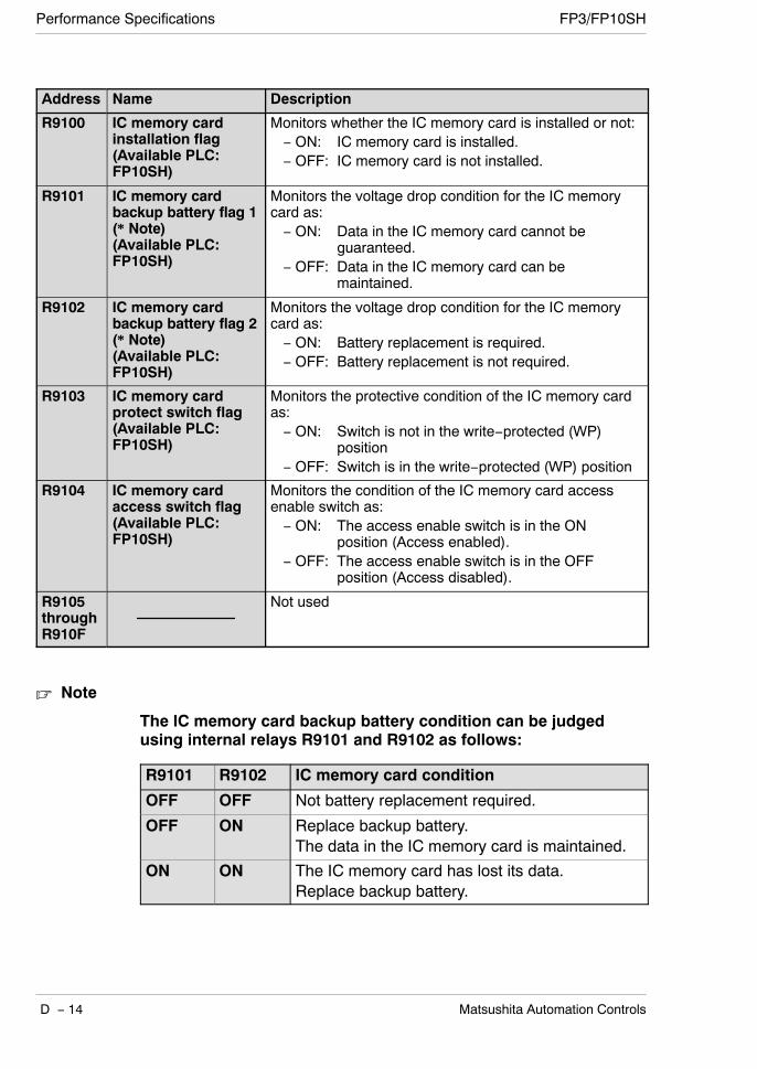
Performance Specifications FP3/FP10SH
D − 14 Matsushita Automation Controls
Address Name Description
R9100 IC memory cardinstallation flag(Available PLC:FP10SH)
Monitors whether the IC memory card is installed or not:− ON: IC memory card is installed.− OFF: IC memory card is not installed.
R9101 IC memory cardbackup battery flag 1(* Note)(Available PLC:FP10SH)
Monitors the voltage drop condition for the IC memorycard as:− ON: Data in the IC memory card cannot be
guaranteed.− OFF: Data in the IC memory card can be
maintained.
R9102 IC memory cardbackup battery flag 2(* Note)(Available PLC:FP10SH)
Monitors the voltage drop condition for the IC memorycard as:− ON: Battery replacement is required.− OFF: Battery replacement is not required.
R9103 IC memory cardprotect switch flag(Available PLC:FP10SH)
Monitors the protective condition of the IC memory cardas:− ON: Switch is not in the write−protected (WP)
position− OFF: Switch is in the write−protected (WP) position
R9104 IC memory cardaccess switch flag(Available PLC:FP10SH)
Monitors the condition of the IC memory card accessenable switch as:− ON: The access enable switch is in the ON
position (Access enabled).− OFF: The access enable switch is in the OFF
position (Access disabled).
R9105throughR910F
Not used
Note
The IC memory card backup battery condition can be judgedusing internal relays R9101 and R9102 as follows:
R9101 R9102 IC memory card condition
OFF OFF Not battery replacement required.
OFF ON Replace backup battery.The data in the IC memory card is maintained.
ON ON The IC memory card has lost its data.Replace backup battery.

Appendix E
Table of Special Data Registers

Performance Specifications FP3/FP10SH
E − 2 Matsushita Automation Controls
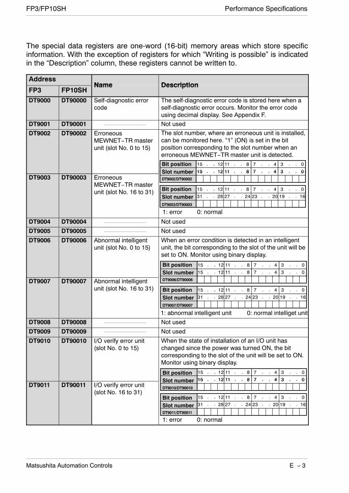
Performance SpecificationsFP3/FP10SH
E − 3Matsushita Automation Controls
The special data registers are one-word (16-bit) memory areas which store specificinformation. With the exception of registers for which “Writing is possible” is indicatedin the “Description” column, these registers cannot be written to.
AddressName Description
FP3 FP10SHName Description
DT9000 DT90000 Self-diagnostic errorcode
The self-diagnostic error code is stored here when aself-diagnostic error occurs. Monitor the error codeusing decimal display. See Appendix F.
DT9001 DT90001 Not used
DT9002 DT90002 ErroneousMEWNET−TR masterunit (slot No. 0 to 15)
· · ··
··
··
· ··
·Slot numberBit position · · · · ·15 12 11 8 7 4 3 0
15 12 11 8 7 4 3 0
The slot number, where an erroneous unit is installed,can be monitored here. “1” (ON) is set in the bitposition corresponding to the slot number when anerroneous MEWNET−TR master unit is detected.
DT9003 DT90003 ErroneousMEWNET−TR masterunit (slot No. 16 to 31)
·
·
·
·
·
·
·
·
·
··
·
··
·
··
·
·
Slot number
·Slot numberBit position · · · · ·
DT9002/DT90002
DT9003/DT90003
15 12 11 8 7 4 3 0
15 12 11 8 7 4 3 0
31 28 27 24 23 20 19 16
1: error 0: normal
DT9004 DT90004 Not used
DT9005 DT90005 Not used
DT9006 DT90006 Abnormal intelligentunit (slot No. 0 to 15)
· · ··
··
··
· ··
·Slot numberBit position · · · · ·15 12 11 8 7 4 3 0
15 12 11 8 7 4 3 0
When an error condition is detected in an intelligentunit, the bit corresponding to the slot of the unit will beset to ON. Monitor using binary display.
DT9007 DT90007 Abnormal intelligentunit (slot No. 16 to 31)
· · · ··
··
··
· ··
Slot numberBit position · · · · ·
DT9006/DT90006
DT9007/DT90007
15 12 11 8 7 4 3 0
31 28 27 24 23 20 19 16
1: abnormal intelligent unit 0: normal intelliget unit
DT9008 DT90008 Not used
DT9009 DT90009 Not used
DT9010 DT90010 I/O verify error unit(slot No. 0 to 15)
· · ··
··
··
· ··
·Slot numberBit position · · · · ·15 12 11 8 7 4 3 0
15 12 11 8 7 4 3 0
When the state of installation of an I/O unit haschanged since the power was turned ON, the bitcorresponding to the slot of the unit will be set to ON.Monitor using binary display.
DT9011 DT90011 I/O verify error unit(slot No. 16 to 31)
·
·
·
·
·
·
·
·
·
··
·
··
·
··
·
·
Slot number
·
Slot numberBit position · · · · ·
DT9010/DT90010
DT9011/DT90011
15 12 11 8 7 4 3 0
15 12 11 8 7 4 3 0
31 28 27 24 23 20 19 16
1: error 0: normal
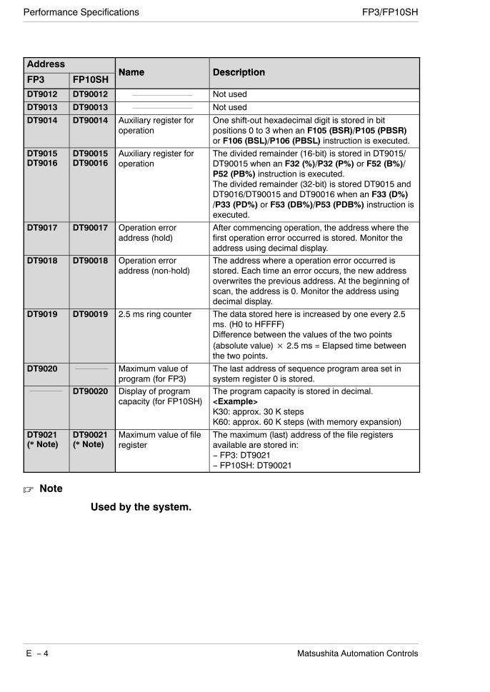
Performance Specifications FP3/FP10SH
E − 4 Matsushita Automation Controls
AddressName Description
FP3 FP10SHName Description
DT9012 DT90012 Not used
DT9013 DT90013 Not used
DT9014 DT90014 Auxiliary register foroperation
One shift-out hexadecimal digit is stored in bitpositions 0 to 3 when an F105 (BSR)/P105 (PBSR)or F106 (BSL)/P106 (PBSL) instruction is executed.
DT9015DT9016
DT90015DT90016
Auxiliary register foroperation
The divided remainder (16-bit) is stored in DT9015/DT90015 when an F32 (%)/P32 (P%) or F52 (B%)/P52 (PB%) instruction is executed.The divided remainder (32-bit) is stored DT9015 andDT9016/DT90015 and DT90016 when an F33 (D%)/P33 (PD%) or F53 (DB%)/P53 (PDB%) instruction isexecuted.
DT9017 DT90017 Operation erroraddress (hold)
After commencing operation, the address where thefirst operation error occurred is stored. Monitor theaddress using decimal display.
DT9018 DT90018 Operation erroraddress (non-hold)
The address where a operation error occurred isstored. Each time an error occurs, the new addressoverwrites the previous address. At the beginning ofscan, the address is 0. Monitor the address usingdecimal display.
DT9019 DT90019 2.5 ms ring counter The data stored here is increased by one every 2.5ms. (H0 to HFFFF)Difference between the values of the two points(absolute value)× 2.5 ms = Elapsed time betweenthe two points.
DT9020 Maximum value ofprogram (for FP3)
The last address of sequence program area set insystem register 0 is stored.
DT90020 Display of programcapacity (for FP10SH)
The program capacity is stored in decimal.<Example>K30: approx. 30 K stepsK60: approx. 60 K steps (with memory expansion)
DT9021(* Note)
DT90021(* Note)
Maximum value of fileregister
The maximum (last) address of the file registersavailable are stored in:− FP3: DT9021− FP10SH: DT90021
Note
Used by the system.
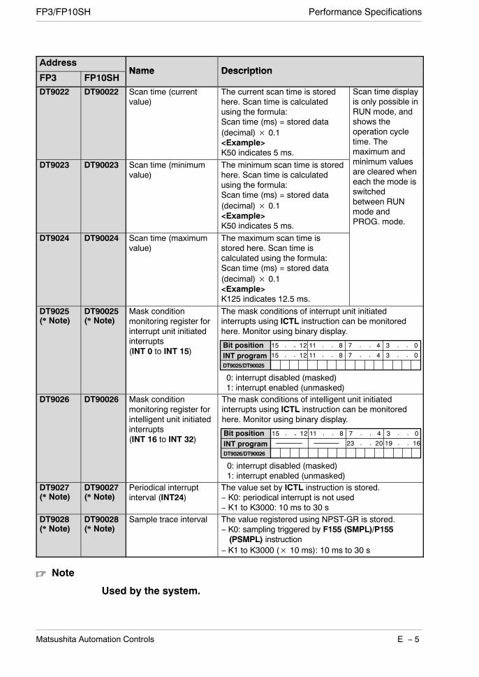
Performance SpecificationsFP3/FP10SH
E − 5Matsushita Automation Controls
AddressName Description
FP3 FP10SHName Description
DT9022 DT90022 Scan time (currentvalue)
The current scan time is storedhere. Scan time is calculatedusing the formula:Scan time (ms) = stored data(decimal)× 0.1<Example>K50 indicates 5 ms.
Scan time displayis only possible inRUN mode, andshows theoperation cycletime. Themaximum andi i lDT9023 DT90023 Scan time (minimum
value)The minimum scan time is storedhere. Scan time is calculatedusing the formula:Scan time (ms) = stored data(decimal)× 0.1<Example>K50 indicates 5 ms.
minimum valuesare cleared wheneach the mode isswitchedbetween RUNmode andPROG. mode.
DT9024 DT90024 Scan time (maximumvalue)
The maximum scan time isstored here. Scan time iscalculated using the formula:Scan time (ms) = stored data(decimal)× 0.1<Example>K125 indicates 12.5 ms.
DT9025(* Note)
DT90025(* Note)
Mask conditionmonitoring register forinterrupt unit initiatedinterrupts(INT 0 to INT 15)
The mask conditions of interrupt unit initiatedinterrupts using ICTL instruction can be monitoredhere. Monitor using binary display.
· · ··
··
··
· ··
·INT programBit position · · · · ·
DT9025/DT90025
15 12 11 8 7 4 3 0
15 12 11 8 7 4 3 0
0: interrupt disabled (masked)1: interrupt enabled (unmasked)
DT9026 DT90026 Mask conditionmonitoring register forintelligent unit initiatedinterrupts(INT 16 to INT 32)
The mask conditions of intelligent unit initiatedinterrupts using ICTL instruction can be monitoredhere. Monitor using binary display.
· ··
·· ·
··INT program
Bit position · · · · ·
DT9026/DT90026
15 12 11 8 7 4 3 0
0: interrupt disabled (masked)1: interrupt enabled (unmasked)
23 20 19 16
DT9027(* Note)
DT90027(* Note)
Periodical interruptinterval (INT24)
The value set by ICTL instruction is stored.− K0: periodical interrupt is not used− K1 to K3000: 10 ms to 30 s
DT9028(* Note)
DT90028(* Note)
Sample trace interval The value registered using NPST-GR is stored.− K0: sampling triggered by F155 (SMPL)/P155(PSMPL) instruction
− K1 to K3000 (× 10 ms): 10 ms to 30 s
Note
Used by the system.

Performance Specifications FP3/FP10SH
E − 6 Matsushita Automation Controls
AddressName Description
FP3 FP10SHName Description
DT9029(* Note)
DT90029(* Note)
Break address The address (K constant) of a break in a test run isstored.
DT9030(* Note)
DT90030(* Note)
Message 0 The contents of the specified message are stored inthese special data registers when an F149
DT9031(* Note)
DT90031(* Note)
Message 1p g
(MSG)/P149 (PMSG) instruction is executed.
DT9032(* Note)
DT90032(* Note)
Message 2
DT9033(* Note)
DT90033(* Note)
Message 3
DT9034(* Note)
DT90034(* Note)
Message 4
DT9035(* Note)
DT90035(* Note)
Message 5
DT9036 DT90036 F152 (RMRD)/P152(PRMRD) and F153(RMWT)/P153(PRMWT) instructionsend code
The error code is stored here if an F152(RMRD)/P152 (PRMRD) or F153 (RMWT)/P153(PRMWT) instruction was executed abnormally.When the instruction was successfully executed “0” isstored.− Other than K0: error code is stored.Refer to the description for the F152 (RMRD)/P152(PRMRD) and F153 (RMWT)/P153 (PRMWT)instructions and the MEWNET-F (REMOTE I/O)SYSTEM manual.
Abnormal unit display If an abnormal unit is installed to the backplane, theslot number of that unit will be stored. Monitor usingdecimal display.
DT9037 DT90037 Work 1 for F96 (SRC)/P96 (PSRC)instructions
The number of found data is stored here when an F96(SRC)/P96 (PSRC) instruction is executed.
DT9038 DT90038 Work 2 for F96(SRC)/P96 (PSRC)instructions
The data position, found in the first place countingfrom the first 16-bit area, is stored here when an F96(SRC)/P96 (PSRC) instruction is executed.
DT9039 DT90039 F145 (SEND)/P145(PSEND) and F146(RECV)/P146 (PRECV)instructions end code
The error code is stored here if an F145 (SEND)/P145 (PSEND) or F146 (RECV)/P146 (PRECV)instruction was executed abnormally.− K0: instruction was successfully executed.− Other than K0: error code is stored.Refer to the description for the F145 (SEND)/P145(PSEND) and F146 (RECV)/P146 (PRECV)instructions and the manual of MEWNET link system.
Note
Used by the system.
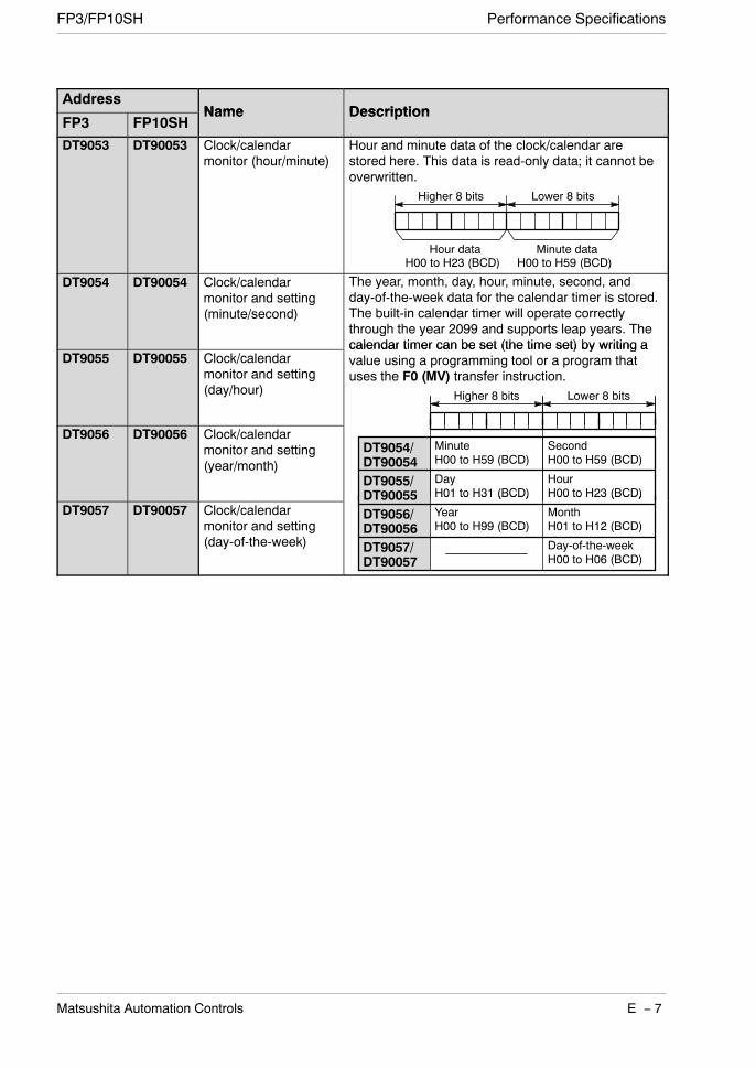
Performance SpecificationsFP3/FP10SH
E − 7Matsushita Automation Controls
AddressName Description
FP3 FP10SHName Description
DT9053 DT90053 Clock/calendarmonitor (hour/minute)
Hour and minute data of the clock/calendar arestored here. This data is read-only data; it cannot beoverwritten.
Higher 8 bits Lower 8 bits
Hour dataH00 to H23 (BCD)
Minute dataH00 to H59 (BCD)
DT9054 DT90054 Clock/calendarmonitor and setting(minute/second)
The year, month, day, hour, minute, second, andday-of-the-week data for the calendar timer is stored.The built-in calendar timer will operate correctlythrough the year 2099 and supports leap years. Thecalendar timer can be set (the time set) by writing a
DT9055 DT90055 Clock/calendarmonitor and setting(day/hour) Higher 8 bits Lower 8 bits
calendar timer can be set (the time set) by writing avalue using a programming tool or a program thatuses the F0 (MV) transfer instruction.
DT9056 DT90056 Clock/calendarmonitor and setting(year/month)
DT9054/DT90054
MinuteH00 to H59 (BCD)
SecondH00 to H59 (BCD)
DT9055/DT90055
DayH01 to H31 (BCD)
HourH00 to H23 (BCD)
DT9057 DT90057 Clock/calendarmonitor and setting(day-of-the-week)
DT90055 H01 to H31 (BCD) H00 to H23 (BCD)
DT9056/DT90056
YearH00 to H99 (BCD)
MonthH01 to H12 (BCD)
DT9057/DT90057
Day-of-the-weekH00 to H06 (BCD)

Performance Specifications FP3/FP10SH
E − 8 Matsushita Automation Controls
AddressName Description
FP3 FP10SHName Description
DT9058(* Note)
DT90058(* Note)
Clock/calendar timesetting and 30scorrection
The clock/calendar is adjusted as follows.When setting the clock/calendar by program thatuses F0 (MV) instructionsBy setting the the highest bit of DT9058/DT90058 to1, the time becomes that written to DT9054 toDT9057/DT90054 to DT90057 by F0 (MV)instruction. After the time is set, DT9058/DT90058 iscleared to 0. (Cannot be performed with anyinstruction other than F0 (MV) instruction.)<EXAMPLE>Set the time to 12:00:00 on the 5th day when the X0turns ON.
Note
If you changed the values of DT9054 toDT9057/DT90054 to DT90057 with the datamonitor functions of NPST-GR software or FPprogrammer II, the time will be set when thenew values are written. Therefore, it isunnecessary to write to DT9058/DT90058.
When the correcting times less than 30 secondsBy setting the lowest bit of DT9058/DT90058 to 1, thevalue will be moved up or down and become exactly0 seconds. After the correction is completed,DT9058/DT90058 is cleared to 0.<EXAMPLE>Correct to 0 seconds with X0 turns ON
At the time of correction, if between 0 and 29seconds, it will be moved down, and if the between30 and 59 seconds, it will be moved up. In theexample above, if the time was 5 minutes 29seconds, it will become 5 minutes 0 second; and, ifthe time was 5 minutes 35 seconds, it will become 6minutes 0 second.
( DF )
[ F0 MV, H 0, DT9054 ]
[ F0 MV, H8000, DT9058 ]
[ F0 MV, H 512, DT9055 ]
1
1X0
Correct to 0second.
Inputs 0. .minutes and 0secondsInputs 12th. .hour 5th daySets the time. .
( DF )
[ F0 MV, H 0, DT9058 ]1
1X0
Note
Used by the system.

Performance SpecificationsFP3/FP10SH
E − 9Matsushita Automation Controls
AddressName Description
FP3 FP10SHName Description
DT9059(* Note)
DT90059(* Note)
Communication errorcode
The error code (decimal) is stored whencommunication error occurs.
Higher 8 bits Lower 8 bits
for RS232C port for tool port
DT9060 DT90060 Step ladder process(0 to 15)
Indicates the startup condition of the step ladderprocess.Wh h h bi diDT9061 DT90061 Step ladder process
(16 to 31)
pWhen the process starts up, the bit corresponding tothe process number turns ON.Monitor using binary display
DT9062 DT90062 Step ladder process(32 to 47)
Monitor using binary display.<Example>
Bit iti 15 12 11 8 7 4 3 0DT9063 DT90063 Step ladder process(48 to 63)
0 0 0 0 0 0 0 0 0 0 0 0 0 0 0 1
·
DT9060/DT90060· · · ··
·· ·
·Process number ··
·
Bit position · · · ·15 12 11 8 7 4 3 015 12 11 8 7 4 3 0
DT9064 DT90064 Step ladder process(64 to 79)
0: not-executing1: executing
0 0 0 0 0 0 0 0 0 0 0 0 0 0 0 1DT9060/DT90060
DT9065 DT90065 Step ladder process(80 to 95)
1: executing
Since bit position 0 of DT9060/DT90060 is “1”, stepladder process 0 is executing
DT9066 DT90066 Step ladder process(96 to 111)
ladder process 0 is executing.A programming tool can be used to write data.
DT9067 DT90067 Step ladder process(112 to 127)
DT9068 DT90068 Step ladder process(128 to 143)
DT9069 DT90069 Step ladder process(144 to 159)
DT9070 DT90070 Step ladder process(160 to 175)
DT9071 DT90071 Step ladder process(176 to 191)
DT9072 DT90072 Step ladder process(192 to 207)
DT9073 DT90073 Step ladder process(208 to 223)
DT9074 DT90074 Step ladder process(224 to 239)
DT9075 DT90075 Step ladder process(240 to 255)
DT9076 DT90076 Step ladder process(256 to 271)
DT9077 DT90077 Step ladder process(272 to 287)
Note
Used by the system.

Performance Specifications FP3/FP10SH
E − 10 Matsushita Automation Controls
AddressName Description
FP3 FP10SHName Description
DT9078 DT90078 Step ladder process(288 to 303)
Indicates the startup condition of the step ladderprocess.Wh h h bi diDT9079 DT90079 Step ladder process
(304 to 319)
pWhen the process starts up, the bit corresponding tothe process number turns ON.Monitor using binary display
DT9080 DT90080 Step ladder process(320 to 335)
Bit iti 15 12 11 8 7 4 3 0
Monitor using binary display.<Example>
DT9081 DT90081 Step ladder process(336 to 351)
0 0 0 0 0 0 0 0 0 0 0 0 0 0 0 1
·
DT9080/DT90080· · · ··
·· ·
·Process number ··
·
Bit position · · · ·15 12 11 8 7 4 3 0335 332 331 328327 324 323 320
DT9082 DT90082 Step ladder process(352 to 367)
0: not-executing,1: executing
0 0 0 0 0 0 0 0 0 0 0 0 0 0 0 1DT9080/DT90080
DT9083 DT90083 Step ladder process(368 to 383)
1: executing
Since bit position 0 of DT9080/DT90080 is “1”, stepladder process 320 is executing
DT9084 DT90084 Step ladder process(384 to 399)
ladder process 320 is executing.A programming tool can be used to write data.
DT9085 DT90085 Step ladder process(400 to 415)
DT9086 DT90086 Step ladder process(416 to 431)
DT9087 DT90087 Step ladder process(432 to 447)
DT9088 DT90088 Step ladder process(448 to 463)
DT9089 DT90089 Step ladder process(464 to 479)
DT9090 DT90090 Step ladder process(480 to 495)
DT9091 DT90091 Step ladder process(496 to 511)
DT9092 DT90092 Step ladder process(512 to 527)
DT9093 DT90093 Step ladder process(528 to 543)
DT9094 DT90094 Step ladder process(544 to 559)
DT9095 DT90095 Step ladder process(560 to 575)
DT9096 DT90096 Step ladder process(576 to 591)
DT9097 DT90097 Step ladder process(592 to 607)
DT9098 DT90098 Step ladder process(608 to 623)
DT9099 DT90099 Step ladder process(624 to 639)
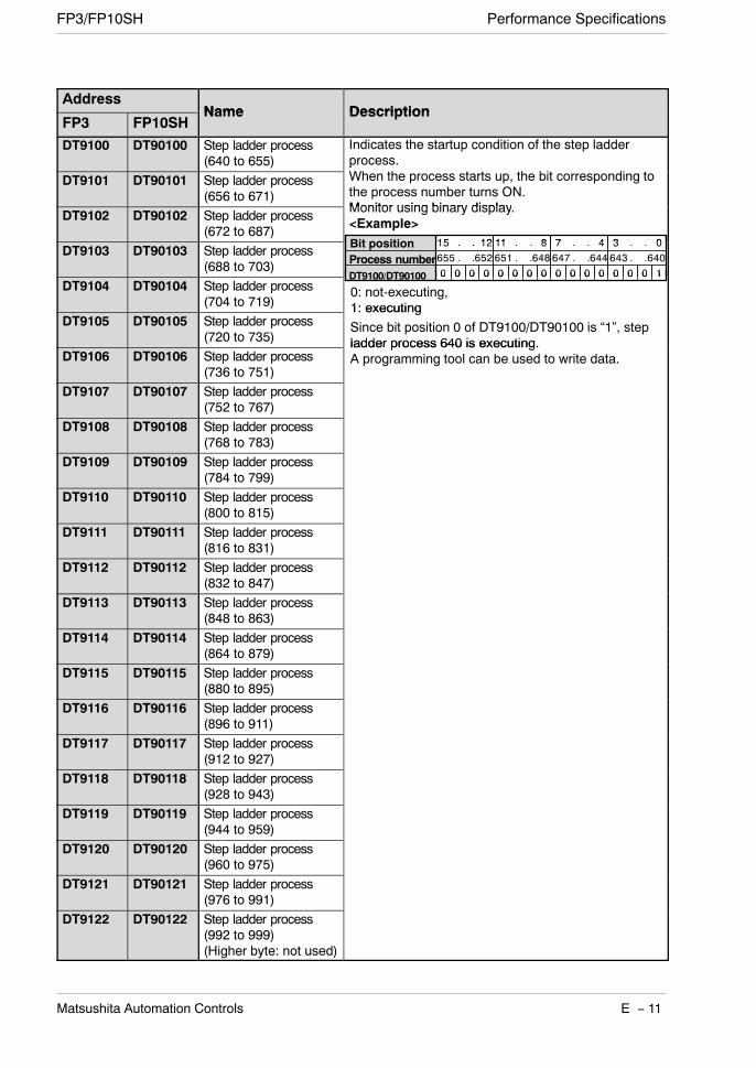
Performance SpecificationsFP3/FP10SH
E − 11Matsushita Automation Controls
AddressName Description
FP3 FP10SHName Description
DT9100 DT90100 Step ladder process(640 to 655)
Indicates the startup condition of the step ladderprocess.Wh h h bi diDT9101 DT90101 Step ladder process
(656 to 671)
pWhen the process starts up, the bit corresponding tothe process number turns ON.Monitor using binary display
DT9102 DT90102 Step ladder process(672 to 687)
Bit position 15 12 11 8 7 4 3 0
Monitor using binary display.<Example>
DT9103 DT90103 Step ladder process(688 to 703) 0 0 0 0 0 0 0 0 0 0 0 0 0 0 0 1
·
DT9100/DT90100· · · ··
·· ·
·Process number ··
·
Bit position · · · ·15 12 11 8 7 4 3 0655 652 651 648 647 644 643 640
DT9104 DT90104 Step ladder process(704 to 719)
0 0 0 0 0 0 0 0 0 0 0 0 0 0 0 1DT9100/DT90100
0: not-executing,1: executing
DT9105 DT90105 Step ladder process(720 to 735)
1: executingSince bit position 0 of DT9100/DT90100 is “1”, stepladder process 640 is executing.
DT9106 DT90106 Step ladder process(736 to 751)
ladder process 640 is executing.A programming tool can be used to write data.
DT9107 DT90107 Step ladder process(752 to 767)
DT9108 DT90108 Step ladder process(768 to 783)
DT9109 DT90109 Step ladder process(784 to 799)
DT9110 DT90110 Step ladder process(800 to 815)
DT9111 DT90111 Step ladder process(816 to 831)
DT9112 DT90112 Step ladder process(832 to 847)
DT9113 DT90113 Step ladder process(848 to 863)
DT9114 DT90114 Step ladder process(864 to 879)
DT9115 DT90115 Step ladder process(880 to 895)
DT9116 DT90116 Step ladder process(896 to 911)
DT9117 DT90117 Step ladder process(912 to 927)
DT9118 DT90118 Step ladder process(928 to 943)
DT9119 DT90119 Step ladder process(944 to 959)
DT9120 DT90120 Step ladder process(960 to 975)
DT9121 DT90121 Step ladder process(976 to 991)
DT9122 DT90122 Step ladder process(992 to 999)(Higher byte: not used)
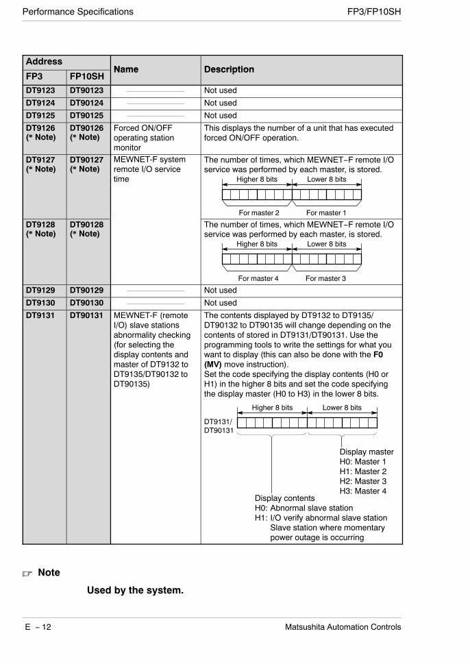
Performance Specifications FP3/FP10SH
E − 12 Matsushita Automation Controls
AddressName Description
FP3 FP10SHName Description
DT9123 DT90123 Not used
DT9124 DT90124 Not used
DT9125 DT90125 Not used
DT9126(* Note)
DT90126(* Note)
Forced ON/OFFoperating stationmonitor
This displays the number of a unit that has executedforced ON/OFF operation.
DT9127(* Note)
DT90127(* Note)
MEWNET-F systemremote I/O servicetime Higher 8 bits Lower 8 bits
For master 2 For master 1
The number of times, which MEWNET−F remote I/Oservice was performed by each master, is stored.
DT9128(* Note)
DT90128(* Note)
Higher 8 bits Lower 8 bits
For master 4 For master 3
The number of times, which MEWNET−F remote I/Oservice was performed by each master, is stored.
DT9129 DT90129 Not used
DT9130 DT90130 Not used
DT9131 DT90131 MEWNET-F (remoteI/O) slave stationsabnormality checking(for selecting thedisplay contents andmaster of DT9132 toDT9135/DT90132 toDT90135)
Higher 8 bits Lower 8 bits
The contents displayed by DT9132 to DT9135/DT90132 to DT90135 will change depending on thecontents of stored in DT9131/DT90131. Use theprogramming tools to write the settings for what youwant to display (this can also be done with the F0(MV) move instruction).Set the code specifying the display contents (H0 orH1) in the higher 8 bits and set the code specifyingthe display master (H0 to H3) in the lower 8 bits.
Display masterH0: Master 1H1: Master 2H2: Master 3H3: Master 4
Display contentsH0: Abnormal slave stationH1: I/O verify abnormal slave station
Slave station where momentarypower outage is occurring
DT9131/DT90131
Note
Used by the system.
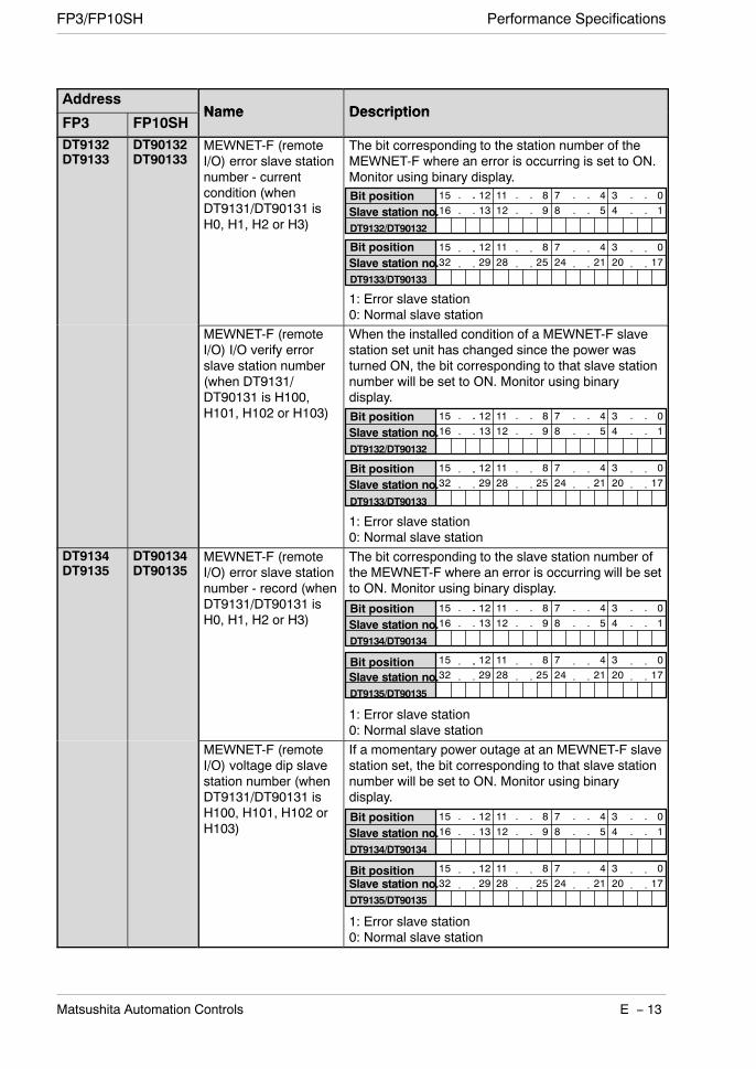
Performance SpecificationsFP3/FP10SH
E − 13Matsushita Automation Controls
AddressName Description
FP3 FP10SHName Description
DT9132DT9133
DT90132DT90133
MEWNET-F (remoteI/O) error slave stationnumber - currentcondition (whenDT9131/DT90131 isH0, H1, H2 or H3)
·
DT9132/DT90132· · · ··
·· ·
·Slave station no. ··
·
Bit position · · · ·15 12 11 8 7 4 3 016 13 12 9 8 5 4 1
The bit corresponding to the station number of theMEWNET-F where an error is occurring is set to ON.Monitor using binary display.
·
DT9133/DT90133· · · ··
·· ·
·Slave station no. ··
·
Bit position · · · ·15 12 11 8 7 4 3 032 29 28 25 24 21 20 17
1: Error slave station0: Normal slave station
MEWNET-F (remoteI/O) I/O verify errorslave station number(when DT9131/DT90131 is H100,H101, H102 or H103) ·
DT9132/DT90132· · · ··
·· ·
·Slave station no. ··
·
Bit position · · · ·15 12 11 8 7 4 3 016 13 12 9 8 5 4 1
When the installed condition of a MEWNET-F slavestation set unit has changed since the power wasturned ON, the bit corresponding to that slave stationnumber will be set to ON. Monitor using binarydisplay.
·
DT9133/DT90133· · · ··
·· ·
·Slave station no. ··
·
Bit position · · · ·15 12 11 8 7 4 3 032 29 28 25 24 21 20 17
1: Error slave station0: Normal slave station
DT9134DT9135
DT90134DT90135
MEWNET-F (remoteI/O) error slave stationnumber - record (whenDT9131/DT90131 isH0, H1, H2 or H3)
·
DT9134/DT90134· · · ··
·· ·
·Slave station no. ··
·
Bit position · · · ·15 12 11 8 7 4 3 016 13 12 9 8 5 4 1
The bit corresponding to the slave station number ofthe MEWNET-F where an error is occurring will be setto ON. Monitor using binary display.
·
DT9135/DT90135· · · ··
·· ·
·Slave station no. ··
·
Bit position · · · ·15 12 11 8 7 4 3 032 29 28 25 24 21 20 17
1: Error slave station0: Normal slave station
MEWNET-F (remoteI/O) voltage dip slavestation number (whenDT9131/DT90131 isH100, H101, H102 orH103)
·
DT9134/DT90134· · · ··
·· ·
·Slave station no. ··
·
Bit position · · · ·15 12 11 8 7 4 3 016 13 12 9 8 5 4 1
If a momentary power outage at an MEWNET-F slavestation set, the bit corresponding to that slave stationnumber will be set to ON. Monitor using binarydisplay.
·
DT9135/DT90135· · · ··
·· ·
·Slave station no. ··
·
Bit position · · · ·15 12 11 8 7 4 3 032 29 28 25 24 21 20 17
1: Error slave station0: Normal slave station

Performance Specifications FP3/FP10SH
E − 14 Matsushita Automation Controls
AddressName Description
FP3 FP10SHName Description
DT9136DT9137
DT90136DT90137
Error code ofMEWNET-F(remote I/O) system
Higher 8 bits Lower 8 bits
For master 2 For master 1
Displays the error conditions for 8 types of errorsusing 1 byte.
Communication error
1: Abnormal condition0: Normal condition
Higher 8 bits Lower 8 bits
For master 4 For master 3
Abnormal I/O unit error
Voltage dip error
I/O mapping error
Slot number error
Terminal station error
Illegal unit errorTransmission error
DT9136/DT90136
DT9137/DT90137
DT9138 DT90138 Not used
DT9139 DT90139 Not used
DT9140(* Note 1)
DT90140(* Note 1)
MEWNET-W/-P PClink status [PC link 0(W/P)] ( N )
The number of times the receiving operation isperformed (counted using ring counter).
DT9141(* Note 1)
DT90141(* Note 1)
[(W/P)] (* Note 2) The current interval between two receiving
operations: value in the register × 2.5msDT9142(* Note 1)
DT90142(* Note 1)
The minimum interval between two receivingoperations: value in the register × 2.5ms
DT9143(* Note 1)
DT90143(* Note 1)
The maximum interval between two receivingoperations: value in the register× 2.5ms
DT9144(* Note 1)
DT90144(* Note 1)
The number of times the sending operation isperformed (counted using ring counter).
DT9145(* Note 1)
DT90145(* Note 1)
The current interval between two sending operations:value in the register × 2.5ms
DT9146(* Note 1)
DT90146(* Note 1)
The minimum interval between two sendingoperations: value in the register × 2.5ms
DT9147(* Note 1)
DT90147(* Note 1)
The maximum interval between two sendingoperations: value in the register × 2.5ms
Notes
(*1):Used by the system.
(*2):When system register 46 = K0, First: PC link 0, second: PC link 1When system register 46 = K1, First: PC link 1, second: PC link 0

Performance SpecificationsFP3/FP10SH
E − 15Matsushita Automation Controls
AddressName Description
FP3 FP10SHName Description
DT9148(* Note 1)
DT90148(* Note 1)
MEWNET-W/-P PClink status [PC link 1(W/P)] ( N )
The number of times the receiving operation isperformed (counted using ring counter).
DT9149(* Note 1)
DT90149(* Note 1)
[(W/P)] (* Note 2) The current interval between two receiving
operations: value in the register × 2.5msDT9150(* Note 1)
DT90150(* Note 1)
The minimum interval between two receivingoperations: value in the register × 2.5ms
DT9151(* Note 1)
DT90151(* Note 1)
The maximum interval between two receivingoperations: value in the register× 2.5ms
DT9152(* Note 1)
DT90152(* Note 1)
The number of times the sending operation isperformed (counted using ring counter).
DT9153(* Note 1)
DT90153(* Note 1)
The current interval between two sending operations:value in the register × 2.5ms
DT9154(* Note 1)
DT90154(* Note 1)
The minimum interval between two sendingoperations: value in the register × 2.5ms
DT9155(* Note 1)
DT90155(* Note 1)
The maximum interval between two sendingoperations: value in the register × 2.5ms
DT9156 DT90156 MEWNET-W/-P PClink status [PC link 0
Area used for measurement of receiving interval.
DT9157 DT90157link status [PC link 0(W/P)] (* Note 2) Area used for measurement of sending interval.
DT9158 DT90158 MEWNET-W/-P PClink status [PC link 1
Area used for measurement of receiving interval.
DT9159 DT90159link status [PC link 1(W/P)] (* Note 2) Area used for measurement of sending interval.
DT9160 DT90160 Link unit No.[W/P link 1]
Stores the unit No. of link 1
DT9161 DT90161 Error flag [W/P link 1] Stores the error flag of link 1
DT9162 DT90162 Link unit No.[W/P link 2]
Stores the unit No. of link 2
DT9163 DT90163 Error flag [W/P link 2] Stores the error flag of link 2
DT9164 DT90164 Link unit No.[W/P link 3]
Stores the unit No. of link 3
DT9165 DT90165 Error flag [W/P link 3] Stores the error flag of link 3
DT9166 DT90166 Not used
DT9167 DT90167 Not used
DT9168 DT90168 Not used
DT9169 DT90169 Not used
Notes
(*1):Used by the system.
(*2):When system register 46 = K0, First: PC link 0, second: PC link 1When system register 46 = K1, First: PC link 1, second: PC link 0
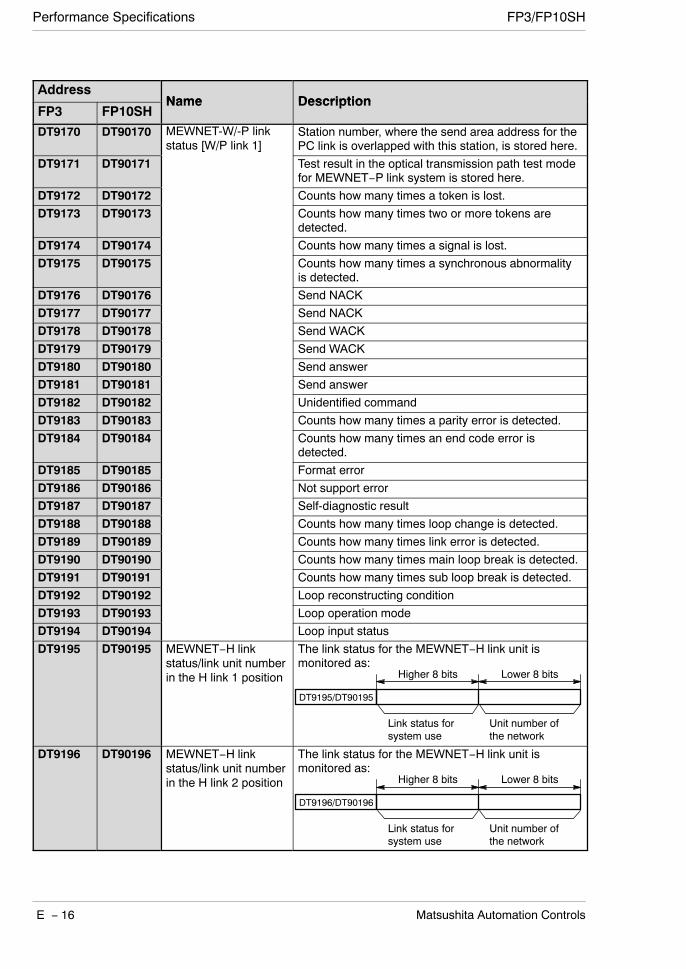
Performance Specifications FP3/FP10SH
E − 16 Matsushita Automation Controls
AddressName Description
FP3 FP10SHName Description
DT9170 DT90170 MEWNET-W/-P linkstatus [W/P link 1]
Station number, where the send area address for thePC link is overlapped with this station, is stored here.
DT9171 DT90171
[ ]
Test result in the optical transmission path test modefor MEWNET−P link system is stored here.
DT9172 DT90172 Counts how many times a token is lost.DT9173 DT90173 Counts how many times two or more tokens are
detected.DT9174 DT90174 Counts how many times a signal is lost.DT9175 DT90175 Counts how many times a synchronous abnormality
is detected.DT9176 DT90176 Send NACKDT9177 DT90177 Send NACKDT9178 DT90178 Send WACKDT9179 DT90179 Send WACKDT9180 DT90180 Send answerDT9181 DT90181 Send answerDT9182 DT90182 Unidentified commandDT9183 DT90183 Counts how many times a parity error is detected.DT9184 DT90184 Counts how many times an end code error is
detected.DT9185 DT90185 Format errorDT9186 DT90186 Not support errorDT9187 DT90187 Self-diagnostic resultDT9188 DT90188 Counts how many times loop change is detected.DT9189 DT90189 Counts how many times link error is detected.DT9190 DT90190 Counts how many times main loop break is detected.DT9191 DT90191 Counts how many times sub loop break is detected.DT9192 DT90192 Loop reconstructing conditionDT9193 DT90193 Loop operation modeDT9194 DT90194 Loop input statusDT9195 DT90195 MEWNET−H link
status/link unit numberin the H link 1 position
The link status for the MEWNET−H link unit ismonitored as:
Higher 8 bits Lower 8 bits
Link status forsystem use
Unit number ofthe network
DT9195/DT90195
DT9196 DT90196 MEWNET−H linkstatus/link unit numberin the H link 2 position
The link status for the MEWNET−H link unit ismonitored as:
Higher 8 bits Lower 8 bits
Link status forsystem use
Unit number ofthe network
DT9196/DT90196
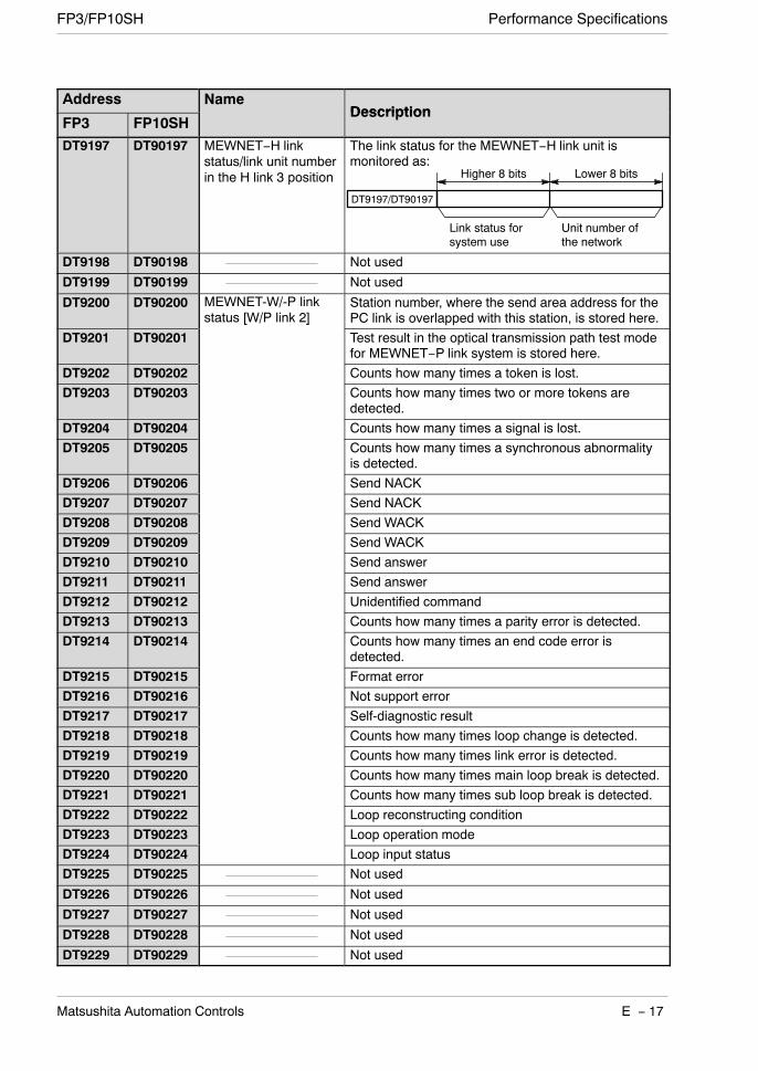
Performance SpecificationsFP3/FP10SH
E − 17Matsushita Automation Controls
Address NameDescription
FP3 FP10SHDescription
DT9197 DT90197 MEWNET−H linkstatus/link unit numberin the H link 3 position
The link status for the MEWNET−H link unit ismonitored as:
Higher 8 bits Lower 8 bits
Link status forsystem use
Unit number ofthe network
DT9197/DT90197
DT9198 DT90198 Not used
DT9199 DT90199 Not used
DT9200 DT90200 MEWNET-W/-P linkstatus [W/P link 2]
Station number, where the send area address for thePC link is overlapped with this station, is stored here.
DT9201 DT90201
[ ]
Test result in the optical transmission path test modefor MEWNET−P link system is stored here.
DT9202 DT90202 Counts how many times a token is lost.DT9203 DT90203 Counts how many times two or more tokens are
detected.DT9204 DT90204 Counts how many times a signal is lost.DT9205 DT90205 Counts how many times a synchronous abnormality
is detected.DT9206 DT90206 Send NACKDT9207 DT90207 Send NACKDT9208 DT90208 Send WACKDT9209 DT90209 Send WACKDT9210 DT90210 Send answerDT9211 DT90211 Send answerDT9212 DT90212 Unidentified commandDT9213 DT90213 Counts how many times a parity error is detected.DT9214 DT90214 Counts how many times an end code error is
detected.DT9215 DT90215 Format errorDT9216 DT90216 Not support errorDT9217 DT90217 Self-diagnostic resultDT9218 DT90218 Counts how many times loop change is detected.DT9219 DT90219 Counts how many times link error is detected.DT9220 DT90220 Counts how many times main loop break is detected.DT9221 DT90221 Counts how many times sub loop break is detected.DT9222 DT90222 Loop reconstructing conditionDT9223 DT90223 Loop operation modeDT9224 DT90224 Loop input statusDT9225 DT90225 Not used
DT9226 DT90226 Not used
DT9227 DT90227 Not used
DT9228 DT90228 Not used
DT9229 DT90229 Not used

Performance Specifications FP3/FP10SH
E − 18 Matsushita Automation Controls
AddressName Description
FP3 FP10SHName Description
DT9230 DT90230 MEWNET-W/-P linkstatus [W/P link 3]
Station number, where the send area address for thePC link is overlapped with this station, is stored here.
DT9231 DT90231
[ ]
Test result in the optical transmission path test modefor MEWNET−P link system is stored here.
DT9232 DT90232 Counts how many times a token is lost.DT9233 DT90233 Counts how many times two or more tokens are
detected.DT9234 DT90234 Counts how many times a signal is lost.DT9235 DT90235 Counts how many times a synchronous abnormality
is detected.DT9236 DT90236 Send NACKDT9237 DT90237 Send NACKDT9238 DT90238 Send WACKDT9239 DT90239 Send WACKDT9240 DT90240 Send answerDT9241 DT90241 Send answerDT9242 DT90242 Unidentified commandDT9243 DT90243 Counts how many times a parity error is detected.DT9244 DT90244 Counts how many times an end code error is
detected.DT9245 DT90245 Format errorDT9246 DT90246 Not support errorDT9247 DT90247 Self-diagnostic resultDT9248 DT90248 Counts how many times loop change is detected.DT9249 DT90249 Counts how many times link error is detected.DT9250 DT90250 Counts how many times main loop break is detected.DT9251 DT90251 Counts how many times sub loop break is detected.DT9252 DT90252 Loop reconstructing conditionDT9253 DT90253 Loop operation modeDT9254 DT90254 Loop input statusDT9255(Not used)
DT90255 Monitoring TOOL portstation number(Available PLC:FP10SH)
Station number (range: H1 to H32) set for FP10SHTOOL (RS232C) port is stored here in the BCDexpression.
DT9256(Not used)
DT90256 Monitoring COM portstation number(Available PLC:FP10SH)
Station number (range: H1 to H32) set for FP10SHCOM (RS232C) port is stored here in the BCDexpression.
DT9257(Not used)
DT90257 Operation errorprogram number(hold)(Available PLC:FP10SH)
An operation error program block number is storedhere when an operation error is detected.Program block number− H1: In the first program block− H2: In the 2nd program block
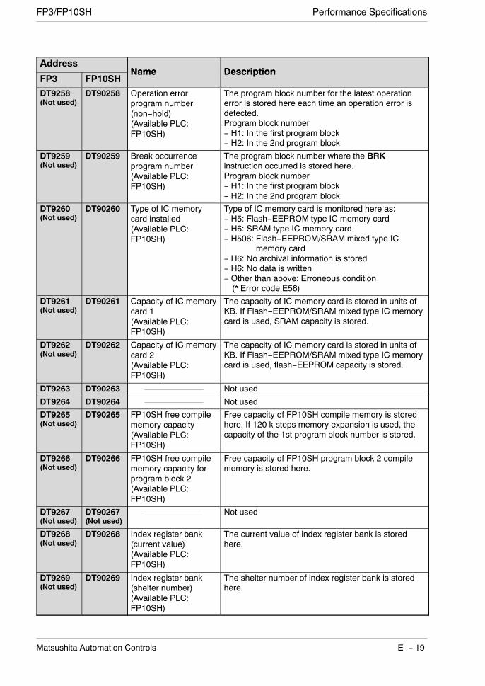
Performance SpecificationsFP3/FP10SH
E − 19Matsushita Automation Controls
AddressName Description
FP3 FP10SHName Description
DT9258(Not used)
DT90258 Operation errorprogram number(non−hold)(Available PLC:FP10SH)
The program block number for the latest operationerror is stored here each time an operation error isdetected.Program block number− H1: In the first program block− H2: In the 2nd program block
DT9259(Not used)
DT90259 Break occurrenceprogram number(Available PLC:FP10SH)
The program block number where the BRKinstruction occurred is stored here.Program block number− H1: In the first program block− H2: In the 2nd program block
DT9260(Not used)
DT90260 Type of IC memorycard installed(Available PLC:FP10SH)
Type of IC memory card is monitored here as:− H5: Flash−EEPROM type IC memory card− H6: SRAM type IC memory card− H506: Flash−EEPROM/SRAM mixed type IC
memory card− H6: No archival information is stored− H6: No data is written− Other than above: Erroneous condition(* Error code E56)
DT9261(Not used)
DT90261 Capacity of IC memorycard 1(Available PLC:FP10SH)
The capacity of IC memory card is stored in units ofKB. If Flash−EEPROM/SRAM mixed type IC memorycard is used, SRAM capacity is stored.
DT9262(Not used)
DT90262 Capacity of IC memorycard 2(Available PLC:FP10SH)
The capacity of IC memory card is stored in units ofKB. If Flash−EEPROM/SRAM mixed type IC memorycard is used, flash−EEPROM capacity is stored.
DT9263 DT90263 Not used
DT9264 DT90264 Not used
DT9265(Not used)
DT90265 FP10SH free compilememory capacity(Available PLC:FP10SH)
Free capacity of FP10SH compile memory is storedhere. If 120 k steps memory expansion is used, thecapacity of the 1st program block number is stored.
DT9266(Not used)
DT90266 FP10SH free compilememory capacity forprogram block 2(Available PLC:FP10SH)
Free capacity of FP10SH program block 2 compilememory is stored here.
DT9267(Not used)
DT90267(Not used)
Not used
DT9268(Not used)
DT90268 Index register bank(current value)(Available PLC:FP10SH)
The current value of index register bank is storedhere.
DT9269(Not used)
DT90269 Index register bank(shelter number)(Available PLC:FP10SH)
The shelter number of index register bank is storedhere.
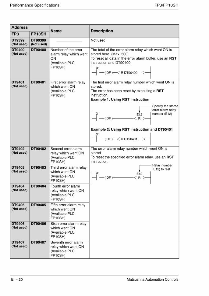
Performance Specifications FP3/FP10SH
E − 20 Matsushita Automation Controls
AddressName Description
FP3 FP10SHName Description
DT9399(Not used)
DT90399(Not used)
Not used
DT9400(Not used)
DT90400 Number of the erroralarm relay which wentON(Available PLC:FP10SH)
The total of the error alarm relay which went ON isstored here. (Max. 500)To reset all data in the error alarm buffer, use an RSTinstruction and DT90400.
( DF ) R DT90400X1
DT9401(Not used)
DT90401 First error alarm relaywhich went ON(Available PLC:FP10SH)
The first error alarm relay number which went ON isstored.The error has been reset by executing a RSTinstruction.Example 1: Using RST instruction
Example 2: Using RST instruction and DT90401
Specify the storederror alarm relaynumber (E12)
( DF )E12R
X1
( DF ) R DT90401X1
DT9402(Not used)
DT90402 Second error alarmrelay which went ON(Available PLC:FP10SH)
The error alarm relay number which went ON isstored.To reset the specified error alarm relay, ues an RSTinstruction.
Relay numberDT9403(Not used)
DT90403 Third error alarm relaywhich went ON(Available PLC:FP10SH)
Relay number(E12) to rest
( DF )E12R
X1
DT9404(Not used)
DT90404 Fourth error alarmrelay which went ON(Available PLC:FP10SH)
DT9405(Not used)
DT90405 Fifth error alarm relaywhich went ON(Available PLC:FP10SH)
DT9406(Not used)
DT90406 Sixth error alarm relaywhich went ON(Available PLC:FP10SH)
DT9407(Not used)
DT90407 Seventh error alarmrelay which went ON(Available PLC:FP10SH)
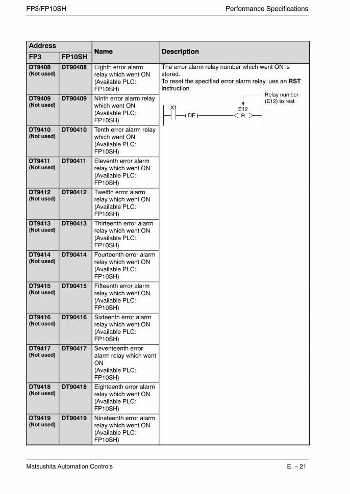
Performance SpecificationsFP3/FP10SH
E − 21Matsushita Automation Controls
AddressName Description
FP3 FP10SHName Description
DT9408(Not used)
DT90408 Eighth error alarmrelay which went ON(Available PLC:FP10SH)
The error alarm relay number which went ON isstored.To reset the specified error alarm relay, ues an RSTinstruction.
Relay numberDT9409(Not used)
DT90409 Ninth error alarm relaywhich went ON(Available PLC:FP10SH)
Relay number(E12) to rest
( DF )E12R
X1
DT9410(Not used)
DT90410 Tenth error alarm relaywhich went ON(Available PLC:FP10SH)
DT9411(Not used)
DT90411 Eleventh error alarmrelay which went ON(Available PLC:FP10SH)
DT9412(Not used)
DT90412 Twelfth error alarmrelay which went ON(Available PLC:FP10SH)
DT9413(Not used)
DT90413 Thirteenth error alarmrelay which went ON(Available PLC:FP10SH)
DT9414(Not used)
DT90414 Fourteenth error alarmrelay which went ON(Available PLC:FP10SH)
DT9415(Not used)
DT90415 Fifteenth error alarmrelay which went ON(Available PLC:FP10SH)
DT9416(Not used)
DT90416 Sixteenth error alarmrelay which went ON(Available PLC:FP10SH)
DT9417(Not used)
DT90417 Seventeenth erroralarm relay which wentON(Available PLC:FP10SH)
DT9418(Not used)
DT90418 Eighteenth error alarmrelay which went ON(Available PLC:FP10SH)
DT9419(Not used)
DT90419 Nineteenth error alarmrelay which went ON(Available PLC:FP10SH)
Performance Specifications FP3/FP10SH
E − 22 Matsushita Automation Controls
AddressName Description
FP3 FP10SHName Description
DT9420(Not used)
DT90420 Time at which the firsterror alarm relay(DT90401) went ON(for minute andsecond data)(Available PLC:FP10SH)
The minute and second data at which the first erroralarm relay in DT90401 went ON is stored.
DT9421(Not used)
DT90421 Time at which the firsterror alarm relay(DT90401) went ON(for day and hour data)(Available PLC:FP10SH)
The day and hour data at which the first error alarmrelay in DT90401 went ON is stored.
DT9422(Not used)
DT90422 Time at which the firsterror alarm relay(DT90401) went ON(for year and monthdata)(Available PLC:FP10SH)
The year and month data at which the first error alarmrelay in DT90401 went ON is stored.
Appendix F
Table of Error Codes
F.1 Confirmation of Error When the Error LEDTurns ON F − 3. . . . . . . . . . . . . . . . . . . . . . . . . . . . . . .
F.1.1 Confirmation Method F − 3. . . . . . . . . . . . . .
F.1.2 Self-Diagnostic Error F − 3. . . . . . . . . . . . . .
F.1.3 Syntax Check Error F − 4. . . . . . . . . . . . . . .
F.2 Table of Syntax Check Error F − 5. . . . . . . . . . . . . . .
F.3 Table of Self-Diagnostic Error F − 7. . . . . . . . . . . . . .
F.4 Table of Communication Check Error F − 13. . . . . .

Performance Specifications FP3/FP10SH
F − 2 Matsushita Automation Controls
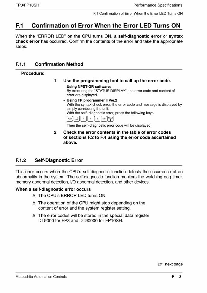
Performance SpecificationsFP3/FP10SH
F − 3Matsushita Automation Controls
F.1 Confirmation of Error When the Error LED Turns ON
F.1 Confirmation of Error When the Error LED Turns ON
When the “ERROR LED” on the CPU turns ON, a self-diagnostic error or syntaxcheck error has occurred. Confirm the contents of the error and take the appropriatesteps.
F.1.1 Confirmation Method
Procedure:
1. Use the programming tool to call up the error code.− Using NPST-GR software:By executing the “STATUS DISPLAY”, the error code and content oferror are displayed.
− Using FP programmer II Ver.2With the syntax check error, the error code and message is displayed bysimply connecting the unit.With the self−diagnostic error, press the following keys.
READ011OP(−)
ACLR ENT
Then the self−diagnostic error code will be displayed.
2. Check the error contents in the table of error codesof sections F.2 to F.4 using the error code ascertainedabove.
F.1.2 Self-Diagnostic Error
This error occurs when the CPU’s self-diagnostic function detects the occurrence of anabnormality in the system. The self-diagnostic function monitors the watching dog timer,memory abnormal detection, I/O abnormal detection, and other devices.
When a self-diagnostic error occurs∆ The CPU’s ERROR LED turns ON.
∆ The operation of the CPU might stop depending on thecontent of error and the system register setting.
∆ The error codes will be stored in the special data registerDT9000 for FP3 and DT90000 for FP10SH.
next page
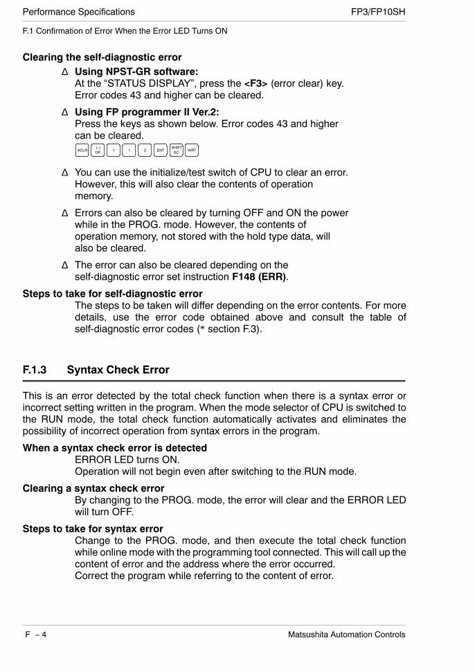
Performance Specifications FP3/FP10SH
F − 4 Matsushita Automation Controls
F.1 Confirmation of Error When the Error LED Turns ON
Clearing the self-diagnostic error∆ Using NPST-GR software:
At the “STATUS DISPLAY”, press the <F3> (error clear) key.Error codes 43 and higher can be cleared.
∆ Using FP programmer II Ver.2:Press the keys as shown below. Error codes 43 and highercan be cleared.
211OP(−)
ACLR ENT WRTSCSHIFT
∆ You can use the initialize/test switch of CPU to clear an error.However, this will also clear the contents of operationmemory.
∆ Errors can also be cleared by turning OFF and ON the powerwhile in the PROG. mode. However, the contents ofoperation memory, not stored with the hold type data, willalso be cleared.
∆ The error can also be cleared depending on theself-diagnostic error set instruction F148 (ERR).
Steps to take for self-diagnostic errorThe steps to be taken will differ depending on the error contents. For moredetails, use the error code obtained above and consult the table ofself-diagnostic error codes (* section F.3).
F.1.3 Syntax Check Error
This is an error detected by the total check function when there is a syntax error orincorrect setting written in the program. When the mode selector of CPU is switched tothe RUN mode, the total check function automatically activates and eliminates thepossibility of incorrect operation from syntax errors in the program.
When a syntax check error is detectedERROR LED turns ON.Operation will not begin even after switching to the RUN mode.
Clearing a syntax check errorBy changing to the PROG. mode, the error will clear and the ERROR LEDwill turn OFF.
Steps to take for syntax errorChange to the PROG. mode, and then execute the total check functionwhile online mode with the programming tool connected. This will call up thecontent of error and the address where the error occurred.Correct the program while referring to the content of error.
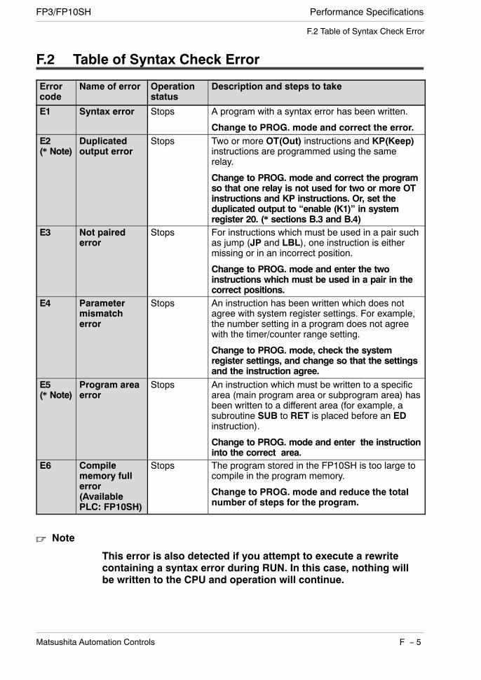
Performance SpecificationsFP3/FP10SH
F − 5Matsushita Automation Controls
F.2 Table of Syntax Check Error
F.2 Table of Syntax Check Error
Errorcode
Name of error Operationstatus
Description and steps to take
E1 Syntax error Stops A program with a syntax error has been written.
Change to PROG. mode and correct the error.E2(* Note)
Duplicatedoutput error
Stops Two or more OT(Out) instructions and KP(Keep)instructions are programmed using the samerelay.
Change to PROG. mode and correct the programso that one relay is not used for two or more OTinstructions and KP instructions. Or, set theduplicated output to “enable (K1)” in systemregister 20. (* sections B.3 and B.4)
E3 Not pairederror
Stops For instructions which must be used in a pair suchas jump (JP and LBL), one instruction is eithermissing or in an incorrect position.
Change to PROG. mode and enter the twoinstructions which must be used in a pair in thecorrect positions.
E4 Parametermismatcherror
Stops An instruction has been written which does notagree with system register settings. For example,the number setting in a program does not agreewith the timer/counter range setting.
Change to PROG. mode, check the systemregister settings, and change so that the settingsand the instruction agree.
E5(* Note)
Program areaerror
Stops An instruction which must be written to a specificarea (main program area or subprogram area) hasbeen written to a different area (for example, asubroutine SUB to RET is placed before an EDinstruction).
Change to PROG. mode and enter the instructioninto the correct area.
E6 Compilememory fullerror(AvailablePLC: FP10SH)
Stops The program stored in the FP10SH is too large tocompile in the program memory.
Change to PROG. mode and reduce the totalnumber of steps for the program.
Note
This error is also detected if you attempt to execute a rewritecontaining a syntax error during RUN. In this case, nothing willbe written to the CPU and operation will continue.

Performance Specifications FP3/FP10SH
F − 6 Matsushita Automation Controls
F.2 Table of Syntax Check Error
Errorcode
Name of error Operationstatus
Description and steps to take
E7 High-levelinstructiontype error
Stops In the program, high-level instructions, whichexecute in every scan and at the leading edge ofthe trigger, are programmed to be triggered byone contact [e.g., F0 (MV) and P0 (PMV) areprogrammed using the same trigger continuously].
Correct the program so that the high-levelinstructions executed in every scan and onlyat the leading edge are triggered separately.
E8 High-levelinstructionoperand error
Stops There is an incorrect operand in an instructionwhich requires a specific combination operands(for example, the operands must all be of a certaintype).
Enter the correct combination of operands.E9 No program
error(AvailablePLC: FP10SH)
Stops Program may be damaged.
Try to send the program again usingNPST-GR.
E10 Rewriteduring RUNsyntax error
Continues When inputting with the ladder symbol mode ofNPST-GR, a deletion, addition or change of orderof an instruction (ED, LBL, SUB, RET, INT, IRET,SSTP, and STPE) that cannot perform a rewriteduring RUN is being attempted. Nothing is writtento the CPU.
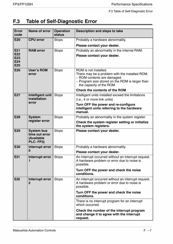
Performance SpecificationsFP3/FP10SH
F − 7Matsushita Automation Controls
F.3 Table of Self-Diagnostic Error
F.3 Table of Self-Diagnostic Error
Errorcode
Name of error Operationstatus
Description and steps to take
E20 CPU error Stops Probably a hardware abnormality.
Please contact your dealer.E21E22E23E24E25
RAM error Stops Probably an abnormality in the internal RAM.
Please contact your dealer.
E26 User’s ROMerror
Stops ROM is not installed.There may be a problem with the installed ROM.− ROM contents are damaged− Program size stored on the ROM is larger thanthe capacity of the ROM
Check the contents of the ROME27 Intelligent unit
installationerror
Stops Intelligent units installed exceed the limitations(i.e., 4 or more link units)
Turn OFF the power and re-configureintelligent units referring to the hardwaremanual.
E28 Systemregister error
Stops Probably an abnormality in the system register.
Check the system register setting or initializethe system registers.
E29 System bustime out error(AvailablePLC: FP3)
Stops Please contact your dealer.
E30 Interrupt error0
Stops Probably a hardware abnormality.
Please contact your dealer.E31 Interrupt error
1Stops An interrupt occurred without an interrupt request.
A hardware problem or error due to noise ispossible.
Turn OFF the power and check the noiseconditions.
E32 Interrupt error2
Stops An interrupt occurred without an interrupt request.A hardware problem or error due to noise ispossible.
Turn OFF the power and check the noiseconditions.There is no interrupt program for an interruptwhich occurred.
Check the number of the interrupt programand change it to agree with the interruptrequest.
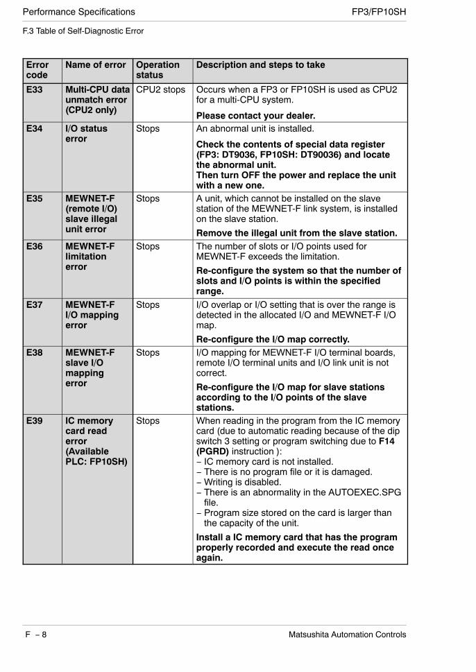
Performance Specifications FP3/FP10SH
F − 8 Matsushita Automation Controls
F.3 Table of Self-Diagnostic Error
Errorcode
Name of error Operationstatus
Description and steps to take
E33 Multi-CPU dataunmatch error(CPU2 only)
CPU2 stops Occurs when a FP3 or FP10SH is used as CPU2for a multi-CPU system.
Please contact your dealer.E34 I/O status
errorStops An abnormal unit is installed.
Check the contents of special data register(FP3: DT9036, FP10SH: DT90036) and locatethe abnormal unit.Then turn OFF the power and replace the unitwith a new one.
E35 MEWNET-F(remote I/O)slave illegalunit error
Stops A unit, which cannot be installed on the slavestation of the MEWNET-F link system, is installedon the slave station.
Remove the illegal unit from the slave station.E36 MEWNET-F
limitationerror
Stops The number of slots or I/O points used forMEWNET-F exceeds the limitation.
Re-configure the system so that the number ofslots and I/O points is within the specifiedrange.
E37 MEWNET-FI/O mappingerror
Stops I/O overlap or I/O setting that is over the range isdetected in the allocated I/O and MEWNET-F I/Omap.
Re-configure the I/O map correctly.E38 MEWNET-F
slave I/Omappingerror
Stops I/O mapping for MEWNET-F I/O terminal boards,remote I/O terminal units and I/O link unit is notcorrect.
Re-configure the I/O map for slave stationsaccording to the I/O points of the slavestations.
E39 IC memorycard readerror(AvailablePLC: FP10SH)
Stops When reading in the program from the IC memorycard (due to automatic reading because of the dipswitch 3 setting or program switching due to F14(PGRD) instruction ):− IC memory card is not installed.− There is no program file or it is damaged.−Writing is disabled.− There is an abnormality in the AUTOEXEC.SPGfile.
− Program size stored on the card is larger thanthe capacity of the unit.
Install a IC memory card that has the programproperly recorded and execute the read onceagain.

Performance SpecificationsFP3/FP10SH
F − 9Matsushita Automation Controls
F.3 Table of Self-Diagnostic Error
Errorcode
Name of error Operationstatus
Description and steps to take
E40 MEWNET-TRcommunica−tion error
Selectable(usingsystemregister 21)
Erroneous MEWNET-TR master unit is detected.
Check the contents of special data registers(FP3: DT9002 and DT9003, FP10SH: DT90002and DT90003) and locate the output unit withblown fuse or the erroneous MEWNET-TRmaster unit. Then replace the fuse or check theunit.
Selection of operation status usingsystem register 21:− to continue execution, set K1 (CONT)− to stop execution, set K0 (STOP)
E41 Intelligent uniterror
Selectable(usingsystemregister 22)
An abnormality in an intelligent unit.
Check the contents of special data registers(FP3: DT9006 and DT9007, FP10SH: DT90006and DT90007) and locate the abnormalintelligent unit. Then check the unit referring toits manual.
Selection of operation status usingsystem register 22:− to continue execution, set K1 (CONT)− to stop execution, set K0 (STOP)
E42 I/O unit verifyerror
Selectable(usingsystemregister 23)
I/O unit wiring condition has changed compared tothat at time of power-up.
Check the contents of special data registers(FP3: DT9010 and DT9011, FP10SH: DT90010and DT90011) and locate the erroneous unit.Then check the unit and correct the wiring.
Selection of operation status usingsystem register 23:− to continue execution, set K1 (CONT)− to stop execution, set K0 (STOP)
E43 Systemwatching dogtimer error(AvailablePLC: FP10SH)
Selectable(usingsystemregister 24)
Selection of operation status usingsystem register 24:− to continue execution, set K1 (CONT)− to stop execution, set K0 (STOP)
Scan time required for program execution exceedsthe setting of the system watching dog timer.
Check the program and modify it so thatFP10SH can execute a scan within the specifiedtime.
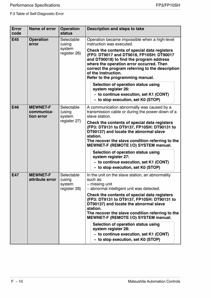
Performance Specifications FP3/FP10SH
F − 10 Matsushita Automation Controls
F.3 Table of Self-Diagnostic Error
Errorcode
Name of error Operationstatus
Description and steps to take
E45 Operationerror
Selectable(usingsystemregister 26)
Operation became impossible when a high-levelinstruction was executed.
Check the contents of special data registers(FP3: DT9017 and DT9018, FP10SH: DT90017and DT90018) to find the program addresswhere the operation error occurred. Thencorrect the program referring to the descriptionof the instruction.Refer to the programming manual.
Selection of operation status usingsystem register 26:− to continue execution, set K1 (CONT)− to stop execution, set K0 (STOP)
E46 MEWNET-Fcommunica-tion error
Selectable(usingsystemregister 27)
A communication abnormally was caused by atransmission cable or during the power-down of aslave station.
Check the contents of special data registers(FP3: DT9131 to DT9137, FP10SH: DT90131 toDT90137) and locate the abnormal slavestation.The recover the slave condition referring to theMEWNET-F (REMOTE I/O) SYSTEM manual.
Selection of operation status usingsystem register 27:− to continue execution, set K1 (CONT)− to stop execution, set K0 (STOP)
E47 MEWNET-Fattribute error
Selectable(usingsystemregister 28)
In the unit on the slave station, an abnormalitysuch as:−missing unit− abnormal intelligent unit was detected.
Check the contents of special data registers(FP3: DT9131 to DT9137, FP10SH: DT90131 toDT90137) and locate the abnormal slavestation.The recover the slave condition referring to theMEWNET-F (REMOTE I/O) SYSTEM manual.
Selection of operation status usingsystem register 28:− to continue execution, set K1 (CONT)− to stop execution, set K0 (STOP)
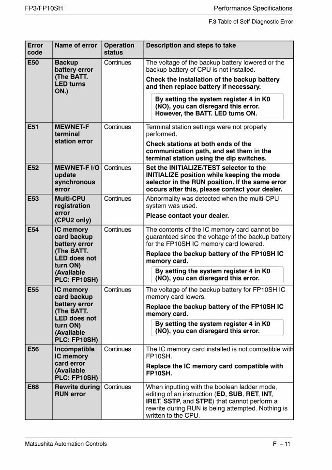
Performance SpecificationsFP3/FP10SH
F − 11Matsushita Automation Controls
F.3 Table of Self-Diagnostic Error
Errorcode
Name of error Operationstatus
Description and steps to take
E50 Backupbattery error(The BATT.LED turnsON.)
Continues The voltage of the backup battery lowered or thebackup battery of CPU is not installed.
Check the installation of the backup batteryand then replace battery if necessary.
By setting the system register 4 in K0(NO), you can disregard this error.However, the BATT. LED turns ON.
E51 MEWNET-Fterminalstation error
Continues Terminal station settings were not properlyperformed.
Check stations at both ends of thecommunication path, and set them in theterminal station using the dip switches.
E52 MEWNET-F I/Oupdatesynchronouserror
Continues Set the INITIALIZE/TEST selector to theINITIALIZE position while keeping the modeselector in the RUN position. If the same erroroccurs after this, please contact your dealer.
E53 Multi-CPUregistrationerror(CPU2 only)
Continues Abnormality was detected when the multi-CPUsystem was used.
Please contact your dealer.
E54 IC memorycard backupbattery error(The BATT.LED does notturn ON)(AvailablePLC: FP10SH)
Continues The contents of the IC memory card cannot beguaranteed since the voltage of the backup batteryfor the FP10SH IC memory card lowered.
Replace the backup battery of the FP10SH ICmemory card.
By setting the system register 4 in K0(NO), you can disregard this error.
E55 IC memorycard backupbattery error(The BATT.LED does notturn ON)(AvailablePLC: FP10SH)
Continues The voltage of the backup battery for FP10SH ICmemory card lowers.
Replace the backup battery of the FP10SH ICmemory card.
By setting the system register 4 in K0(NO), you can disregard this error.
E56 IncompatibleIC memorycard error(AvailablePLC: FP10SH)
Continues The IC memory card installed is not compatible withFP10SH.
Replace the IC memory card compatible withFP10SH.
E68 Rewrite duringRUN error
Continues When inputting with the boolean ladder mode,editing of an instruction (ED, SUB, RET, INT,IRET, SSTP, and STPE) that cannot perform arewrite during RUN is being attempted. Nothing iswritten to the CPU.

Performance Specifications FP3/FP10SH
F − 12 Matsushita Automation Controls
F.3 Table of Self-Diagnostic Error
Errorcode
Name of error Operationstatus
Description and steps to take
E100toE199
Self-diagnosticerror set by
/
Stops The self-diagnostic error specified by the F148(ERR)/P148 (PERR) instruction is occurred.
Take steps to clear the error conditionE200toE299
yF148 (ERR)/P148 (PERR)instruction
ContinuesTake steps to clear the error conditionaccording to the specification you chose.
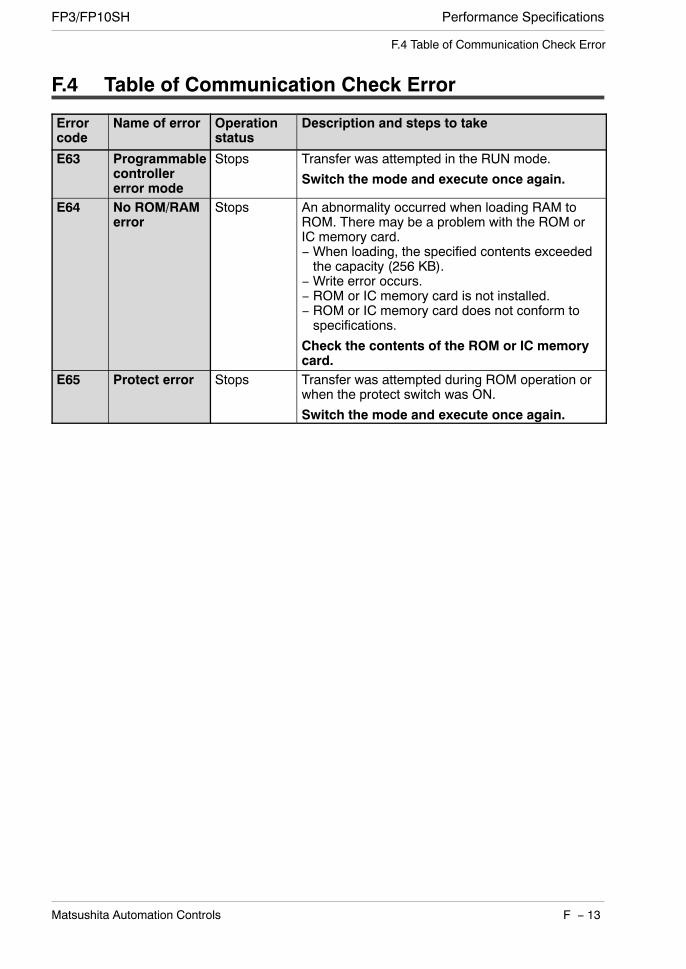
Performance SpecificationsFP3/FP10SH
F − 13Matsushita Automation Controls
F.4 Table of Communication Check Error
F.4 Table of Communication Check Error
Errorcode
Name of error Operationstatus
Description and steps to take
E63 Programmablecontrollererror mode
Stops Transfer was attempted in the RUN mode.
Switch the mode and execute once again.
E64 No ROM/RAMerror
Stops An abnormality occurred when loading RAM toROM. There may be a problem with the ROM orIC memory card.−When loading, the specified contents exceededthe capacity (256 KB).
−Write error occurs.− ROM or IC memory card is not installed.− ROM or IC memory card does not conform tospecifications.
Check the contents of the ROM or IC memorycard.
E65 Protect error Stops Transfer was attempted during ROM operation orwhen the protect switch was ON.
Switch the mode and execute once again.

Performance Specifications FP3/FP10SH
F − 14 Matsushita Automation Controls
F.4 Table of Communication Check Error

Appendix G
Table of Instructions
G.1 Table of Basic Instructions G − 3. . . . . . . . . . . . . . . .
G.2 Table of High-Level Instructions G − 17. . . . . . . . . .

Performance Specifications FP3/FP10SH
G − 2 Matsushita Automation Controls
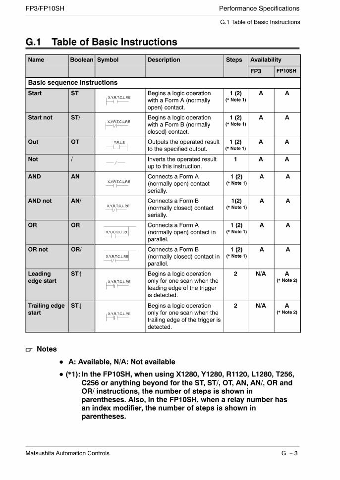
Performance SpecificationsFP3/FP10SH
G − 3Matsushita Automation Controls
G.1 Table of Basic Instructions
G.1 Table of Basic Instructions
Name Boolean Symbol Description Steps Availability
FP3 FP10SH
Basic sequence instructions
Start STX,Y,R,T,C,L,P,E
Begins a logic operationwith a Form A (normallyopen) contact.
1 (2)(* Note 1)
A A
Start not ST/X,Y,R,T,C,L,P,E
Begins a logic operationwith a Form B (normallyclosed) contact.
1 (2)(* Note 1)
A A
Out OT Y,R,L,E Outputs the operated resultto the specified output.
1 (2)(* Note 1)
A A
Not / Inverts the operated resultup to this instruction.
1 A A
AND ANX,Y,R,T,C,L,P,E
Connects a Form A(normally open) contactserially.
1 (2)(* Note 1)
A A
AND not AN/X,Y,R,T,C,L,P,E
Connects a Form B(normally closed) contactserially.
1(2)(* Note 1)
A A
OR ORX,Y,R,T,C,L,P,E
Connects a Form A(normally open) contact inparallel.
1 (2)(* Note 1)
A A
OR not OR/X,Y,R,T,C,L,P,E
Connects a Form B(normally closed) contact inparallel.
1 (2)(* Note 1)
A A
Leadingedge start
ST↑X,Y,R,T,C,L,P,E↑
Begins a logic operationonly for one scan when theleading edge of the triggeris detected.
2 N/A A(* Note 2)
Trailing edgestart
ST↓X,Y,R,T,C,L,P,E↓
Begins a logic operationonly for one scan when thetrailing edge of the trigger isdetected.
2 N/A A(* Note 2)
Notes
A: Available, N/A: Not available
(*1): In the FP10SH, when using X1280, Y1280, R1120, L1280, T256,C256 or anything beyond for the ST, ST/, OT, AN, AN/, OR andOR/ instructions, the number of steps is shown inparentheses. Also, in the FP10SH, when a relay number hasan index modifier, the number of steps is shown inparentheses.

Performance Specifications FP3/FP10SH
G − 4 Matsushita Automation Controls
(*2):This instruction should be input using NPST−GR Ver.4.0 orlater.
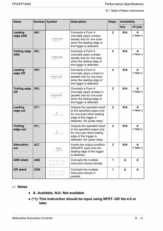
Performance SpecificationsFP3/FP10SH
G − 5Matsushita Automation Controls
G.1 Table of Basic Instructions
Name Boolean Symbol Description Steps Availability
FP3 FP10SH
Leadingedge AND
AN↑
X,Y,R,T,C,L,P,E↑
Connects a Form A(normally open) contactserially only for one scanwhen the leading edge ofthe trigger is detected.
2 N/A A(* Note 1)
Trailing edgeAND
AN↓
X,Y,R,T,C,L,P,E↓
Connects a Form A(normally open) contactserially only for one scanwhen the trailing edge ofthe trigger is detected.
2 N/A A(* Note 1)
Leadingedge OR
OR↑
X,Y,R,T,C,L,P,E↑
Connects a Form A(normally open) contact inparallel only for one scanwhen the leading edge ofthe trigger is detected.
2 N/A A(* Note 1)
Trailing edgeOR
OR↓
X,Y,R,T,C,L,P,E↓
Connects a Form A(normally open) contact inparallel only for one scanwhen the trailing edge ofthe trigger is detected.
2 N/A A(* Note 1)
Leadingedge out
OT↑
P
↑
Outputs the operated resultto the specified output onlyfor one scan when leadingedge of the trigger isdetected. (for pulse relay)
2 N/A A(* Note 1)
Trailingedge out
OT↓
P↓
Outputs the operated resultto the specified output onlyfor one scan when trailingedge of the trigger isdetected. (for pulse relay)
2 N/A A(* Note 1)
Alternativeout
ALTY,R,L,EA
Inverts the output condition(ON/OFF) each time theleading edge of the triggeris detected.
3 N/A A(* Note 1)
AND stack ANS Connects the multipleinstruction blocks serially.
1 A A
OR stack ORS Connects the multipleinstruction blocks inparallel.
1 A A
Notes
A: Available, N/A: Not available
(*1):This instruction should be input using NPST−GR Ver.4.0 orlater.
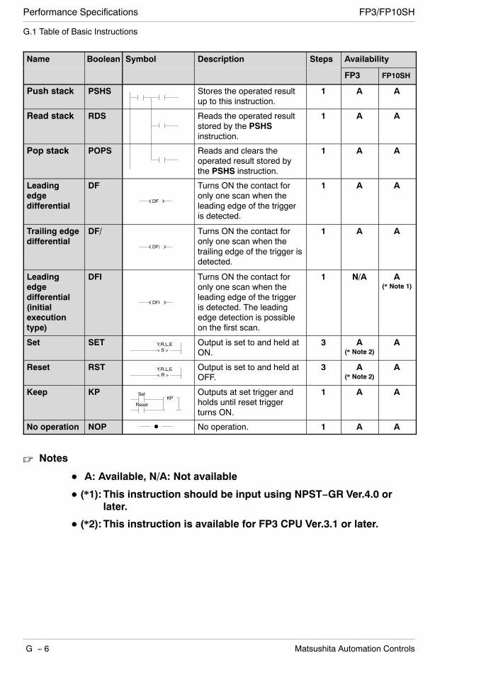
Performance Specifications FP3/FP10SH
G − 6 Matsushita Automation Controls
G.1 Table of Basic Instructions
Name Boolean Symbol Description Steps Availability
FP3 FP10SH
Push stack PSHS Stores the operated resultup to this instruction.
1 A A
Read stack RDS Reads the operated resultstored by the PSHSinstruction.
1 A A
Pop stack POPS Reads and clears theoperated result stored bythe PSHS instruction.
1 A A
Leadingedgedifferential
DF
(DF )
Turns ON the contact foronly one scan when theleading edge of the triggeris detected.
1 A A
Trailing edgedifferential
DF/
(DF/ )
Turns ON the contact foronly one scan when thetrailing edge of the trigger isdetected.
1 A A
Leadingedgedifferential(initialexecutiontype)
DFI
(DFI )
Turns ON the contact foronly one scan when theleading edge of the triggeris detected. The leadingedge detection is possibleon the first scan.
1 N/A A(* Note 1)
Set SET< S >Y,R,L,E Output is set to and held at
ON.3 A
(* Note 2)A
Reset RST< R >Y,R,L,E Output is set to and held at
OFF.3 A
(* Note 2)A
Keep KP Set
ResetKP
Outputs at set trigger andholds until reset triggerturns ON.
1 A A
No operation NOP ・ No operation. 1 A A
Notes
A: Available, N/A: Not available
(*1):This instruction should be input using NPST−GR Ver.4.0 orlater.
(*2):This instruction is available for FP3 CPU Ver.3.1 or later.
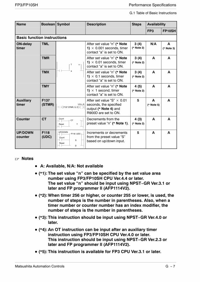
Performance SpecificationsFP3/FP10SH
G − 7Matsushita Automation Controls
G.1 Table of Basic Instructions
Name Boolean Symbol Description Steps Availability
FP3 FP10SH
Basic function instructions
ON-delaytimer
TML After set value “n” (* Note1)× 0.001 seconds, timercontact “a” is set to ON.
3 (4)(* Note 2)
N/A A(* Note 3)
TMR
T n
After set value “n” (* Note1)× 0.01 seconds, timercontact “a” is set to ON.
3 (4)(* Note 2)
A A
TMX a After set value “n” (* Note1)× 0.1 seconds, timercontact “a” is set to ON.
3 (4)(* Note 2)
A A
TMY After set value “n” (* Note1)× 1 second, timercontact “a” is set to ON.
4 (5)(* Note 2)
A A
Auxiliarytimer
F137(STMR) Y,R,L,E
F137 STMR, S, D
After set value “S”× 0.01seconds, the specifiedoutput (* Note 4) andR900D are set to ON.
5 A(* Note 5)
A
Counter CT Count
Reset
CT
n
Decrements from thepreset value “n” (* Note 1).
4 (3)(* Note 2)
A A
UP/DOWNcounter
F118(UDC)
UP/DOWN
Count
F118 UDC
ResetS
D
Increments or decrementsfrom the preset value “S”based on up/down input.
5 A A
Notes
A: Available, N/A: Not available
(*1):The set value “n” can be specified by the set value areanumber using FP3/FP10SH CPU Ver.4.4 or later.The set value “n” should be input using NPST−GR Ver.3.1 orlater and FP programmer II (AFP1114V2).
(*2):When timer 256 or higher, or counter 255 or lower, is used, thenumber of steps is the number in parentheses. Also, when atimer number or counter number has an index modifier, thenumber of steps is the number in parentheses.
(*3):This instruction should be input using NPST−GR Ver.4.0 orlater.
(*4):An OT instruction can be input after an auxiliary timerinstruction using FP3/FP10SH CPU Ver.4.0 or later.This instruction should be input using NPST−GR Ver.2.3 orlater and FP programmer II (AFP1114V2).
(*5):This instruction is available for FP3 CPU Ver.3.1 or later.
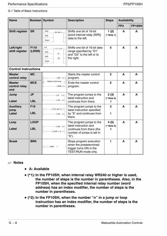
Performance Specifications FP3/FP10SH
G − 8 Matsushita Automation Controls
G.1 Table of Basic Instructions
Name Boolean Symbol Description Steps Availability
FP3 FP10SH
Shift register SR Data
Shift
SR WR n
Reset
Shifts one bit of 16-bit[word internal relay (WR)]data to the left.
1 (2)(* Note 1)
A A
Left/rightshift register
F119(LRSR) Data
Shift
Reset
L/RF119 LRSR
D1
D2
Shifts one bit of 16-bit datarange specified by “D1”and “D2” to the left or tothe right.
5 A A
Control instructions
Mastercontrol relay
MC(MC n)
Starts the master controlprogram.
2 A A
Mastercontrol relayend
MCE(MCE n)
Master control areaEnds the master controlprogram.
2 A A
Jump
Label
JP
LBL
(JP n)
(LBL n)
The program jumps to thelabel instruction andcontinues from there.
2 (3)(* Note 2)
1
A A
AuxiliaryjumpLabel
F19
LBL (LBL n)
F19 SJP SThe program jumps to thelabel instruction specifiedby “S” and continues fromthere.
3
1
A A
Loop
Label
LOOP
LBL(LBL n)
LOOP n, S
The program jumps to thelabel instruction andcontinues from there (thenumber of jumps is set in“S”).
4 (5)(* Note 2)
1
A A
Break BRK
(BRK )
Stops program executionwhen the predeterminedtrigger turns ON in theTEST/RUN mode only.
1 A A
Notes
A: Available
(*1): In the FP10SH, when internal relay WR240 or higher is used,the number of steps is the number in parentheses. Also, in theFP10SH, when the specified internal relay number (wordaddress) has an index modifier, the number of steps is thenumber in parentheses.
(*2): In the FP10SH, when the number “n” in a jump or loopinstruction has an index modifier, the number of steps is thenumber in parentheses.
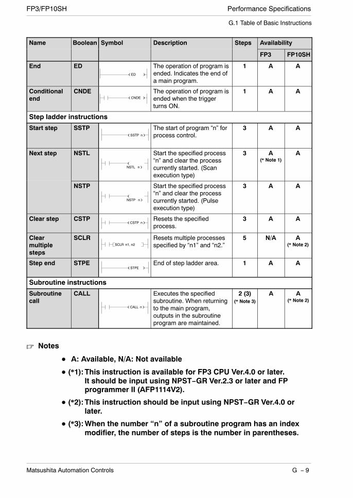
Performance SpecificationsFP3/FP10SH
G − 9Matsushita Automation Controls
G.1 Table of Basic Instructions
Name Boolean Symbol Description Steps Availability
FP3 FP10SH
End ED(ED )
The operation of program isended. Indicates the end ofa main program.
1 A A
Conditionalend
CNDE(CNDE )
The operation of program isended when the triggerturns ON.
1 A A
Step ladder instructions
Start step SSTP The start of program “n” forprocess control.
3 A A
Next step NSTL Start the specified process“n” and clear the processcurrently started. (Scanexecution type)
3 A(* Note 1)
A
NSTP Start the specified process“n” and clear the processcurrently started. (Pulseexecution type)
3 A A
Clear step CSTP Resets the specifiedprocess.
3 A A
Clearmultiplesteps
SCLR Resets multiple processesspecified by “n1” and “n2.”
5 N/A A(* Note 2)
Step end STPE End of step ladder area. 1 A A
Subroutine instructions
Subroutinecall
CALL Executes the specifiedsubroutine. When returningto the main program,outputs in the subroutineprogram are maintained.
2 (3)(* Note 3)
A A(* Note 2)
Notes
A: Available, N/A: Not available
(*1):This instruction is available for FP3 CPU Ver.4.0 or later.It should be input using NPST−GR Ver.2.3 or later and FPprogrammer II (AFP1114V2).
(*2):This instruction should be input using NPST−GR Ver.4.0 orlater.
(*3):When the number “n” of a subroutine program has an indexmodifier, the number of steps is the number in parentheses.
(SSTP n)
(NSTL n)
(NSTP n)
(CSTP n)
(STPE )
SCLR n1, n2
(CALL n)

Performance Specifications FP3/FP10SH
G − 10 Matsushita Automation Controls
G.1 Table of Basic Instructions
Name Boolean Symbol Description Steps Availability
FP3 FP10SH
Output OFFtypesubroutinecall
FCAL Executes the specifiedsubroutine. When returningto the main program, alloutputs in the subroutineprogram are set to OFF.
4 N/A A(* Note 1)
Subroutineentry
SUB Indicates the start of thesubroutine program.
1 A A
Subroutinereturn
RET Ends the subroutineprogram.
1 A A
Interrupt instructions
Interrupt INT Indicates the start of theinterrupt program.
1 A A
Interruptreturn
IRET Ends the interrupt program. 1 A A
Interruptcontrol
ICTL Select interruptenable/disable or clear in“S1” and “S2” and execute.
5 A A
Notes
A: Available, N/A: Not available
(*1):This instruction should be input using NPST−GR Ver.4.0 orlater.
ICTL S1, S2(DF)
(FCAL n)
(SUB n)
(RET )
(INT n)
(IRET )
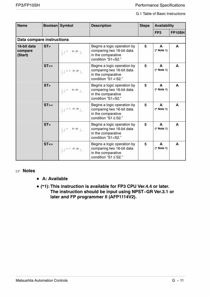
Performance SpecificationsFP3/FP10SH
G − 11Matsushita Automation Controls
G.1 Table of Basic Instructions
Name Boolean Symbol Description Steps Availability
FP3 FP10SH
Data compare instructions
16-bit datacompare(Start)
ST= Begins a logic operation bycomparing two 16-bit datain the comparativecondition “S1=S2.”
5 A(* Note 1)
A
ST<> Begins a logic operation bycomparing two 16-bit datain the comparativecondition “S1≠S2.”
5 A(* Note 1)
A
ST> Begins a logic operation bycomparing two 16-bit datain the comparativecondition “S1>S2.”
5 A(* Note 1)
A
ST>= Begins a logic operation bycomparing two 16-bit datain the comparativecondition “S1≧S2.”
5 A(* Note 1)
A
ST< Begins a logic operation bycomparing two 16-bit datain the comparativecondition “S1<S2.”
5 A(* Note 1)
A
ST<= Begins a logic operation bycomparing two 16-bit datain the comparativecondition “S1≦S2.”
5 A(* Note 1)
A
Notes
A: Available
(*1):This instruction is available for FP3 CPU Ver.4.4 or later.The instruction should be input using NPST−GR Ver.3.1 orlater and FP programmer II (AFP1114V2).
= S1, S2
< > S1, S2
> S1, S2
> = S1, S2
< S1, S2
< = S1, S2
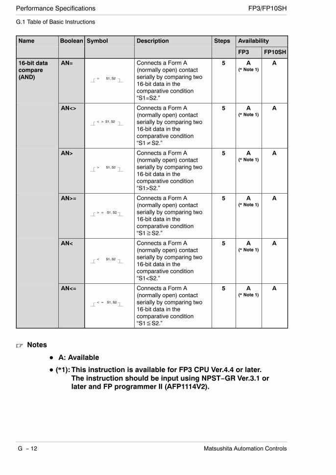
Performance Specifications FP3/FP10SH
G − 12 Matsushita Automation Controls
G.1 Table of Basic Instructions
Name Boolean Symbol Description Steps Availability
FP3 FP10SH
16-bit datacompare(AND)
AN= Connects a Form A(normally open) contactserially by comparing two16-bit data in thecomparative condition“S1=S2.”
5 A(* Note 1)
A
AN<> Connects a Form A(normally open) contactserially by comparing two16-bit data in thecomparative condition“S1≠S2.”
5 A(* Note 1)
A
AN> Connects a Form A(normally open) contactserially by comparing two16-bit data in thecomparative condition“S1>S2.”
5 A(* Note 1)
A
AN>= Connects a Form A(normally open) contactserially by comparing two16-bit data in thecomparative condition“S1≧S2.”
5 A(* Note 1)
A
AN< Connects a Form A(normally open) contactserially by comparing two16-bit data in thecomparative condition“S1<S2.”
5 A(* Note 1)
A
AN<= Connects a Form A(normally open) contactserially by comparing two16-bit data in thecomparative condition“S1≦S2.”
5 A(* Note 1)
A
Notes
A: Available
(*1):This instruction is available for FP3 CPU Ver.4.4 or later.The instruction should be input using NPST−GR Ver.3.1 orlater and FP programmer II (AFP1114V2).
= S1, S2
< > S1, S2
> S1, S2
> = S1, S2
< S1, S2
< = S1, S2
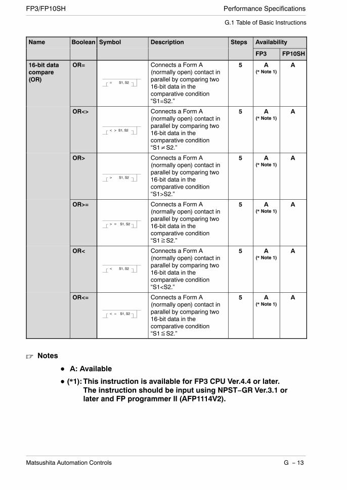
Performance SpecificationsFP3/FP10SH
G − 13Matsushita Automation Controls
G.1 Table of Basic Instructions
Name Boolean Symbol Description Steps Availability
FP3 FP10SH
16-bit datacompare(OR)
OR= Connects a Form A(normally open) contact inparallel by comparing two16-bit data in thecomparative condition“S1=S2.”
5 A(* Note 1)
A
OR<> Connects a Form A(normally open) contact inparallel by comparing two16-bit data in thecomparative condition“S1≠S2.”
5 A(* Note 1)
A
OR> Connects a Form A(normally open) contact inparallel by comparing two16-bit data in thecomparative condition“S1>S2.”
5 A(* Note 1)
A
OR>= Connects a Form A(normally open) contact inparallel by comparing two16-bit data in thecomparative condition“S1≧S2.”
5 A(* Note 1)
A
OR< Connects a Form A(normally open) contact inparallel by comparing two16-bit data in thecomparative condition“S1<S2.”
5 A(* Note 1)
A
OR<= Connects a Form A(normally open) contact inparallel by comparing two16-bit data in thecomparative condition“S1≦S2.”
5 A(* Note 1)
A
Notes
A: Available
(*1):This instruction is available for FP3 CPU Ver.4.4 or later.The instruction should be input using NPST−GR Ver.3.1 orlater and FP programmer II (AFP1114V2).
= S1, S2
< > S1, S2
> S1, S2
> = S1, S2
< S1, S2
< = S1, S2
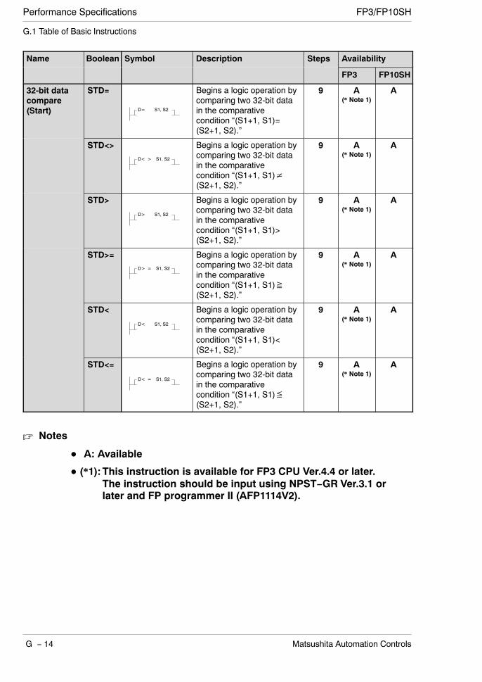
Performance Specifications FP3/FP10SH
G − 14 Matsushita Automation Controls
G.1 Table of Basic Instructions
Name Boolean Symbol Description Steps Availability
FP3 FP10SH
32-bit datacompare(Start)
STD= Begins a logic operation bycomparing two 32-bit datain the comparativecondition “(S1+1, S1)=(S2+1, S2).”
9 A(* Note 1)
A
STD<> Begins a logic operation bycomparing two 32-bit datain the comparativecondition “(S1+1, S1)≠(S2+1, S2).”
9 A(* Note 1)
A
STD> Begins a logic operation bycomparing two 32-bit datain the comparativecondition “(S1+1, S1)>(S2+1, S2).”
9 A(* Note 1)
A
STD>= Begins a logic operation bycomparing two 32-bit datain the comparativecondition “(S1+1, S1)≧(S2+1, S2).”
9 A(* Note 1)
A
STD< Begins a logic operation bycomparing two 32-bit datain the comparativecondition “(S1+1, S1)<(S2+1, S2).”
9 A(* Note 1)
A
STD<= Begins a logic operation bycomparing two 32-bit datain the comparativecondition “(S1+1, S1)≦(S2+1, S2).”
9 A(* Note 1)
A
Notes
A: Available
(*1):This instruction is available for FP3 CPU Ver.4.4 or later.The instruction should be input using NPST−GR Ver.3.1 orlater and FP programmer II (AFP1114V2).
D= S1, S2
D< > S1, S2
D> S1, S2
D> = S1, S2
D< S1, S2
D< = S1, S2
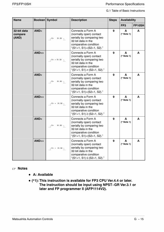
Performance SpecificationsFP3/FP10SH
G − 15Matsushita Automation Controls
G.1 Table of Basic Instructions
Name Boolean Symbol Description Steps Availability
FP3 FP10SH
32-bit datacompare(AND)
AND= Connects a Form A(normally open) contactserially by comparing two32-bit data in thecomparative condition“(S1+1, S1)=(S2+1, S2).”
9 A(* Note 1)
A
AND<> Connects a Form A(normally open) contactserially by comparing two32-bit data in thecomparative condition“(S1+1, S1)≠(S2+1, S2).”
9 A(* Note 1)
A
AND> Connects a Form A(normally open) contactserially by comparing two32-bit data in thecomparative condition“(S1+1, S1)>(S2+1, S2).”
9 A(* Note 1)
A
AND>= Connects a Form A(normally open) contactserially by comparing two32-bit data in thecomparative condition“(S1+1, S1)≧(S2+1, S2).”
9 A(* Note 1)
A
AND< Connects a Form A(normally open) contactserially by comparing two32-bit data in thecomparative condition“(S1+1, S1)<(S2+1, S2).”
9 A(* Note 1)
A
AND<= Connects a Form A(normally open) contactserially by comparing two32-bit data in thecomparative condition“(S1+1, S1)≦(S2+1, S2).”
9 A(* Note 1)
A
Notes
A: Available
(*1):This instruction is available for FP3 CPU Ver.4.4 or later.The instruction should be input using NPST−GR Ver.3.1 orlater and FP programmer II (AFP1114V2).
D= S1, S2
D< > S1, S2
D> S1, S2
D> = S1, S2
D< S1, S2
D< = S1, S2
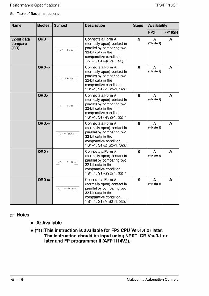
Performance Specifications FP3/FP10SH
G − 16 Matsushita Automation Controls
G.1 Table of Basic Instructions
Name Boolean Symbol Description Steps Availability
FP3 FP10SH
32-bit datacompare(OR)
ORD= Connects a Form A(normally open) contact inparallel by comparing two32-bit data in thecomparative condition“(S1+1, S1)=(S2+1, S2).”
9 A(* Note 1)
A
ORD<> Connects a Form A(normally open) contact inparallel by comparing two32-bit data in thecomparative condition“(S1+1, S1)≠(S2+1, S2).”
9 A(* Note 1)
A
ORD> Connects a Form A(normally open) contact inparallel by comparing two32-bit data in thecomparative condition“(S1+1, S1)>(S2+1, S2).”
9 A(* Note 1)
A
ORD>= Connects a Form A(normally open) contact inparallel by comparing two32-bit data in thecomparative condition“(S1+1, S1)≧(S2+1, S2).”
9 A(* Note 1)
A
ORD< Connects a Form A(normally open) contact inparallel by comparing two32-bit data in thecomparative condition“(S1+1, S1)<(S2+1, S2).”
9 A(* Note 1)
A
ORD<= Connects a Form A(normally open) contact inparallel by comparing two32-bit data in thecomparative condition“(S1+1, S1)≦(S2+1, S2).”
9 A(* Note 1)
A
Notes
A: Available
(*1):This instruction is available for FP3 CPU Ver.4.4 or later.The instruction should be input using NPST−GR Ver.3.1 orlater and FP programmer II (AFP1114V2).
D= S1, S2
D< > S1, S2
D> S1, S2
D> = S1, S2
D< S1, S2
D< = S1, S2

Performance SpecificationsFP3/FP10SH
G − 17Matsushita Automation Controls
G.2 Table of High-Level Instructions
G.2 Table of High-Level Instructions
The high-level instructions for FP3/FP10SH are expressed by the prefixes “F” or “P” withnumbers. For most of the high-level instructions, “F” and “P” types are available. Thedifferences between the two types are explained as follows:
− Instructions with the prefix “F” are executed in every scan while its trigger is inthe ON.
− Instructions with the prefix “P” are executed only when the leading edge of itstrigger is detected.
Number Name Boolean Operand Description Steps Availability
FP3 FP10SH
Data transfer instructions
F0P0
16-bit datamove
MVPMV
S, D (S)→ (D) 5 A A
F1P1
32-bit datamove
DMVPDMV
S, D (S+1, S)→ (D+1, D) 7 A A
F2P2
16-bit datainvert andmove
MV/PMV/
S, D (S)→ (D) 5 A A
F3P3
32-bit datainvert andmove
DMV/PDMV/
S, D (S+1, S)→ (D+1, D) 7 A A
F5P5
Bit data move BTMPBTM
S, n, D The specified one bit in“S” is transferred to thespecified one bit in “D.”The bit is specified by“n.”
7 A A
F6P6
Hexadecimaldigit (4-bit)data move
DGTPDGT
S, n, D The specified one digitin “S” is transferred tothe specified one digit in“D.” The digit isspecified by “n.”
7 A A
F7P7
Two 16-bitdata move
MV2PMV2
S1, S2,D
(S1)→ (D), (S2)→(D+1)
7 N/A A(* Note 1)
F8P8
Two 32-bitdata move
DMV2PDMV2
S1, S2,D
(S1+1, S1)→ (D+1, D),(S2+1, S2)→ (D+3,D+2)
11 N/A A(* Note 1)
F10P10
Block move BKMVPBKMV
S1, S2,D
The data between “S1”and “S2” is transferred tothe area starting at “D.”
7 A A
Notes
A: Available, N/A: Not available

Performance Specifications FP3/FP10SH
G − 18 Matsushita Automation Controls
(*1):The instruction for FP10SH should be input using NPST−GRVer.4.0 or later.
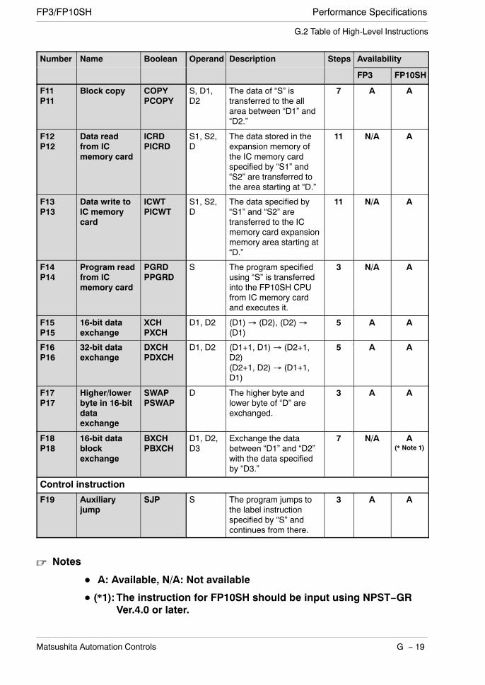
Performance SpecificationsFP3/FP10SH
G − 19Matsushita Automation Controls
G.2 Table of High-Level Instructions
Number Name Boolean Operand Description Steps Availability
FP3 FP10SH
F11P11
Block copy COPYPCOPY
S, D1,D2
The data of “S” istransferred to the allarea between “D1” and“D2.”
7 A A
F12P12
Data readfrom ICmemory card
ICRDPICRD
S1, S2,D
The data stored in theexpansion memory ofthe IC memory cardspecified by “S1” and“S2” are transferred tothe area starting at “D.”
11 N/A A
F13P13
Data write toIC memorycard
ICWTPICWT
S1, S2,D
The data specified by“S1” and “S2” aretransferred to the ICmemory card expansionmemory area starting at“D.”
11 N/A A
F14P14
Program readfrom ICmemory card
PGRDPPGRD
S The program specifiedusing “S” is transferredinto the FP10SH CPUfrom IC memory cardand executes it.
3 N/A A
F15P15
16-bit dataexchange
XCHPXCH
D1, D2 (D1)→ (D2), (D2)→(D1)
5 A A
F16P16
32-bit dataexchange
DXCHPDXCH
D1, D2 (D1+1, D1)→ (D2+1,D2)(D2+1, D2)→ (D1+1,D1)
5 A A
F17P17
Higher/lowerbyte in 16-bitdataexchange
SWAPPSWAP
D The higher byte andlower byte of “D” areexchanged.
3 A A
F18P18
16-bit datablockexchange
BXCHPBXCH
D1, D2,D3
Exchange the databetween “D1” and “D2”with the data specifiedby “D3.”
7 N/A A(* Note 1)
Control instruction
F19 Auxiliaryjump
SJP S The program jumps tothe label instructionspecified by “S” andcontinues from there.
3 A A
Notes
A: Available, N/A: Not available
(*1):The instruction for FP10SH should be input using NPST−GRVer.4.0 or later.

Performance Specifications FP3/FP10SH
G − 20 Matsushita Automation Controls
G.2 Table of High-Level Instructions
Number Name Boolean Operand Description Steps Availability
FP3 FP10SH
Binary arithmetic instructions
F20P20
16-bit dataaddition
+P+
S, D (D) + (S)→ (D) 5 A A
F21P21
32-bit dataaddition
D+PD+
S, D (D +1, D) + (S+1, S)→(D+1, D)
7 A A
F22P22
16-bit dataaddition
+P+
S1, S2,D
(S1) + (S2)→ (D) 7 A A
F23P23
32-bit dataaddition
D+PD+
S1, S2,D
(S1+1, S1) + (S2+1, S2)→ (D+1, D)
11 A A
F25P25
16-bit datasubtraction
−P−
S, D (D) − (S)→ (D) 5 A A
F26P26
32-bit datasubtraction
D−PD−
S, D (D+1, D) − (S+1, S)→(D+1, D)
7 A A
F27P27
16-bit datasubtraction
−P−
S1, S2,D
(S1) − (S2)→ (D) 7 A A
F28P28
32-bit datasubtraction
D−PD−
S1, S2,D
(S1+1, S1) − (S2+1, S2)→ (D+1, D)
11 A A
F30P30
16-bit datamultiplication
*P*
S1, S2,D
(S1)× (S2)→ (D+1, D) 7 A A
F31P31
32-bit datamultiplication
D*PD*
S1, S2,D
(S1+1, S1)× (S2+1,S2)→ (D+3, D+2, D+1,D)
11 A A
F32P32
16-bit datadivision
%P%
S1, S2,D
(S1)÷ (S2)→quotient (D)remainder (DT9015 forFP3 or DT90015 forFP10SH)
7 A A
F33P33
32-bit datadivision
D%PD%
S1, S2,D
[(S1+1, S1)÷ (S2+1,S2)→ quotient (D+1, D)remainder (DT9016,DT9015 for FP3 orDT90016, DT90015 forFP10SH)]
11 A A
F34P34
16-bit datamultiplication(result in 16bits)
*WP*W
S1, S2,D
(S1)× (S2)→ (D) 7 N/A A(* Note 1)
F35P35
16-bit dataincrement
+1P+1
D (D) + 1→ (D) 3 A A
Notes
A: Available, N/A: Not available
(*1):The instruction for FP10SH should be input using NPST−GRVer.4.0 or later.

Performance SpecificationsFP3/FP10SH
G − 21Matsushita Automation Controls
G.2 Table of High-Level Instructions
Number Name Boolean Operand Description Steps Availability
FP3 FP10SH
F36P36
32-bit dataincrement
D+1PD+1
D (D+1, D) + 1→ (D+1, D) 3 A A
F37P37
16-bit datadecrement
−1P−1
D (D) − 1→ (D) 3 A A
F38P38
32-bit datadecrement
D−1PD−1
D (D+1, D) − 1→ (D+1, D) 3 A A
F39P39
32-bit datamultiplication(result in 32bits)
D*DPD*D
S1, S2,D
(S1+1, S1)× (S2+1,S2)→ (D+1, D)
11 N/A A(* Note 1)
BCD arithmetic instructions
F40P40
4-digit BCDdata addition
B+PB+
S, D (D) + (S)→ (D) 5 A A
F41P41
8-digit BCDdata addition
DB+PDB+
S, D (D+1, D) + (S+1, S)→(D+1, D)
7 A A
F42P42
4-digit BCDdata addition
B+PB+
S1, S2,D
(S1) + (S2)→ (D) 7 A A
F43P43
8-digit BCDdata addition
DB+PDB+
S1, S2,D
(S1+1, S1) + (S2+1, S2)→ (D+1, D)
11 A A
F45P45
4-digit BCDdatasubtraction
B−PB−
S, D (D) − (S)→ (D) 5 A A
F46P46
8-digit BCDdatasubtraction
DB−PDB−
S, D (D+1, D) − (S+1, S)→(D+1, D)
7 A A
F47P47
4-digit BCDdatasubtraction
B−PB−
S1, S2,D
(S1) − (S2)→ (D) 7 A A
F48P48
8-digit BCDdatasubtraction
DB−PDB−
S1, S2,D
(S1+1, S1) − (S2+1, S2)→ (D+1, D)
11 A A
F50P50
4-digit BCDdatamultiplication
B*PB*
S1, S2,D
(S1)× (S2)→ (D+1, D) 7 A A
F51P51
8-digit BCDdatamultiplication
DB*PDB*
S1, S2,D
(S1+1, S1)× (S2+1,S2)→ (D+3, D+2, D+1,D)
11 A A
Notes
A: Available, N/A: Not available
(*1):The instruction for FP10SH should be input using NPST−GRVer.4.0 or later.
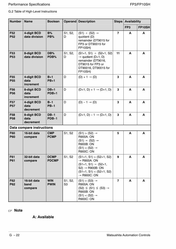
Performance Specifications FP3/FP10SH
G − 22 Matsushita Automation Controls
G.2 Table of High-Level Instructions
Number Name Boolean Operand Description Steps Availability
FP3 FP10SH
F52P52
4-digit BCDdata division
B%PB%
S1, S2,D
(S1)÷ (S2)→quotient (D)remainder (DT9015 forFP3 or DT90015 forFP10SH)
7 A A
F53P53
8-digit BCDdata division
DB%PDB%
S1, S2,D
(S1+1, S1) ÷ (S2+1, S2)→ quotient (D+1, D)remainder (DT9016,DT9015 for FP3 orDT90016, DT90015 forFP10SH)
11 A A
F55P55
4-digit BCDdataincrement
B+1PB+1
D (D) + 1→ (D) 3 A A
F56P56
8-digit BCDdataincrement
DB+1PDB+1
D (D+1, D) + 1→ (D+1, D) 3 A A
F57P57
4-digit BCDdatadecrement
B−1PB−1
D (D) − 1→ (D) 3 A A
F58P58
8-digit BCDdatadecrement
DB−1PDB−1
D (D+1, D) − 1→ (D+1, D) 3 A A
Data compare instructions
F60P60
16-bit datacompare
CMPPCMP
S1, S2 (S1) > (S2)→R900A: ON(S1)= (S2)→R900B: ON(S1) < (S2)→R900C: ON
5 A A
F61P61
32-bit datacompare
DCMPPDCMP
S1, S2 (S1+1, S1) > (S2+1, S2)→ R900A: ON(S1+1, S1)= (S2+1,S2)→ R900B: ON(S1+1, S1) < (S2+1, S2)→ R900C: ON
9 A A
F62P62
16-bit databandcompare
WINPWIN
S1, S2,S3
(S1) > (S3)→R900A: ON(S2)≦ (S1)≦ (S3)→R900B: ON(S1) < (S2)→R900C: ON
7 A A
Note
A: Available
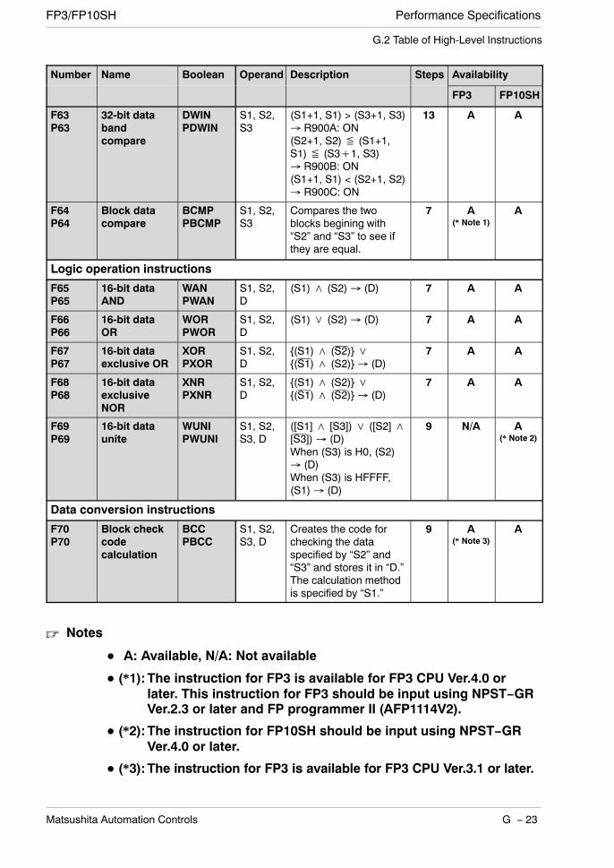
Performance SpecificationsFP3/FP10SH
G − 23Matsushita Automation Controls
G.2 Table of High-Level Instructions
Number Name Boolean Operand Description Steps Availability
FP3 FP10SH
F63P63
32-bit databandcompare
DWINPDWIN
S1, S2,S3
(S1+1, S1) > (S3+1, S3)→ R900A: ON(S2+1, S2)≦ (S1+1,S1)≦ (S3+1, S3)→ R900B: ON(S1+1, S1) < (S2+1, S2)→ R900C: ON
13 A A
F64P64
Block datacompare
BCMPPBCMP
S1, S2,S3
Compares the twoblocks begining with“S2” and “S3” to see ifthey are equal.
7 A(* Note 1)
A
Logic operation instructions
F65P65
16-bit dataAND
WANPWAN
S1, S2,D
(S1)∧ (S2)→ (D) 7 A A
F66P66
16-bit dataOR
WORPWOR
S1, S2,D
(S1)∨ (S2)→ (D) 7 A A
F67P67
16-bit dataexclusive OR
XORPXOR
S1, S2,D
(S1)∧ (S2)∨(S1)∧ (S2)→ (D)
7 A A
F68P68
16-bit dataexclusiveNOR
XNRPXNR
S1, S2,D
(S1)∧ (S2)∨(S1)∧ (S2)→ (D)
7 A A
F69P69
16-bit dataunite
WUNIPWUNI
S1, S2,S3, D
([S1]∧ [S3])∨ ([S2]∧[S3])→ (D)When (S3) is H0, (S2)→ (D)When (S3) is HFFFF,(S1)→ (D)
9 N/A A(* Note 2)
Data conversion instructions
F70P70
Block checkcodecalculation
BCCPBCC
S1, S2,S3, D
Creates the code forchecking the dataspecified by “S2” and“S3” and stores it in “D.”The calculation methodis specified by “S1.”
9 A(* Note 3)
A
Notes
A: Available, N/A: Not available
(*1):The instruction for FP3 is available for FP3 CPU Ver.4.0 orlater. This instruction for FP3 should be input using NPST−GRVer.2.3 or later and FP programmer II (AFP1114V2).
(*2):The instruction for FP10SH should be input using NPST−GRVer.4.0 or later.
(*3):The instruction for FP3 is available for FP3 CPU Ver.3.1 or later.
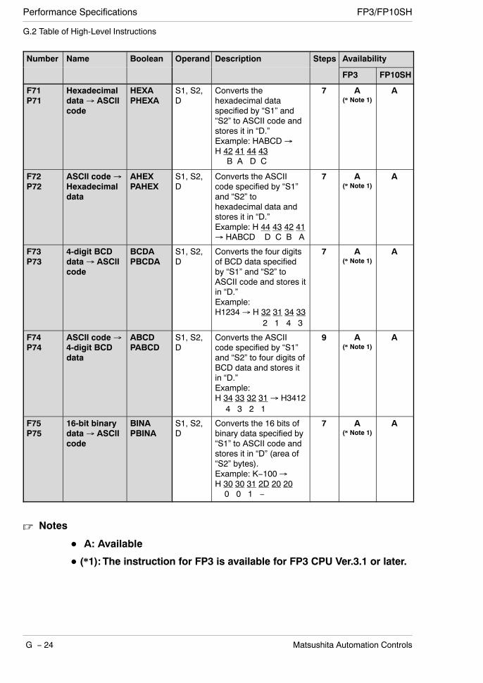
Performance Specifications FP3/FP10SH
G − 24 Matsushita Automation Controls
G.2 Table of High-Level Instructions
Number Name Boolean Operand Description Steps Availability
FP3 FP10SH
F71P71
Hexadecimaldata→ ASCIIcode
HEXAPHEXA
S1, S2,D
Converts thehexadecimal dataspecified by “S1” and“S2” to ASCII code andstores it in “D.”Example: HABCD→H 42 41 44 43
B A D C
7 A(* Note 1)
A
F72P72
ASCII code→Hexadecimaldata
AHEXPAHEX
S1, S2,D
Converts the ASCIIcode specified by “S1”and “S2” tohexadecimal data andstores it in “D.”Example: H 44 43 42 41→ HABCD D C B A
7 A(* Note 1)
A
F73P73
4-digit BCDdata→ ASCIIcode
BCDAPBCDA
S1, S2,D
Converts the four digitsof BCD data specifiedby “S1” and “S2” toASCII code and stores itin “D.”Example:H1234→ H 32 31 34 33
2 1 4 3
7 A(* Note 1)
A
F74P74
ASCII code→4-digit BCDdata
ABCDPABCD
S1, S2,D
Converts the ASCIIcode specified by “S1”and “S2” to four digits ofBCD data and stores itin “D.”Example:H 34 33 32 31→ H3412
4 3 2 1
9 A(* Note 1)
A
F75P75
16-bit binarydata→ ASCIIcode
BINAPBINA
S1, S2,D
Converts the 16 bits ofbinary data specified by“S1” to ASCII code andstores it in “D” (area of“S2” bytes).Example: K−100→H 30 30 31 2D 20 200 0 1 −
7 A(* Note 1)
A
Notes
A: Available
(*1):The instruction for FP3 is available for FP3 CPU Ver.3.1 or later.
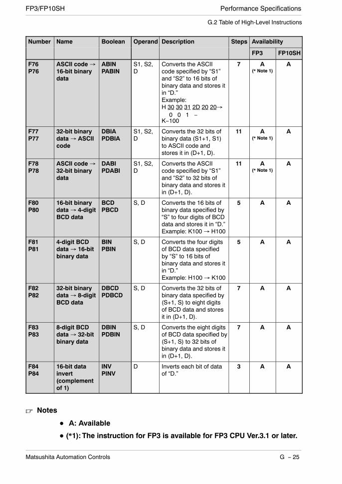
Performance SpecificationsFP3/FP10SH
G − 25Matsushita Automation Controls
G.2 Table of High-Level Instructions
Number Name Boolean Operand Description Steps Availability
FP3 FP10SH
F76P76
ASCII code→16-bit binarydata
ABINPABIN
S1, S2,D
Converts the ASCIIcode specified by “S1”and “S2” to 16 bits ofbinary data and stores itin “D.”Example:H 30 30 31 2D 20 20→
0 0 1 −K−100
7 A(* Note 1)
A
F77P77
32-bit binarydata→ ASCIIcode
DBIAPDBIA
S1, S2,D
Converts the 32 bits ofbinary data (S1+1, S1)to ASCII code andstores it in (D+1, D).
11 A(* Note 1)
A
F78P78
ASCII code→32-bit binarydata
DABIPDABI
S1, S2,D
Converts the ASCIIcode specified by “S1”and “S2” to 32 bits ofbinary data and stores itin (D+1, D).
11 A(* Note 1)
A
F80P80
16-bit binarydata→ 4-digitBCD data
BCDPBCD
S, D Converts the 16 bits ofbinary data specified by“S” to four digits of BCDdata and stores it in “D.”Example: K100→ H100
5 A A
F81P81
4-digit BCDdata→ 16-bitbinary data
BINPBIN
S, D Converts the four digitsof BCD data specifiedby “S” to 16 bits ofbinary data and stores itin “D.”Example: H100→ K100
5 A A
F82P82
32-bit binarydata→ 8-digitBCD data
DBCDPDBCD
S, D Converts the 32 bits ofbinary data specified by(S+1, S) to eight digitsof BCD data and storesit in (D+1, D).
7 A A
F83P83
8-digit BCDdata→ 32-bitbinary data
DBINPDBIN
S, D Converts the eight digitsof BCD data specified by(S+1, S) to 32 bits ofbinary data and stores itin (D+1, D).
7 A A
F84P84
16-bit datainvert(complementof 1)
INVPINV
D Inverts each bit of dataof “D.”
3 A A
Notes
A: Available
(*1):The instruction for FP3 is available for FP3 CPU Ver.3.1 or later.
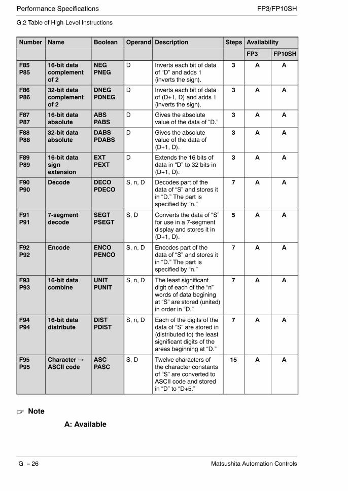
Performance Specifications FP3/FP10SH
G − 26 Matsushita Automation Controls
G.2 Table of High-Level Instructions
Number Name Boolean Operand Description Steps Availability
FP3 FP10SH
F85P85
16-bit datacomplementof 2
NEGPNEG
D Inverts each bit of dataof “D” and adds 1(inverts the sign).
3 A A
F86P86
32-bit datacomplementof 2
DNEGPDNEG
D Inverts each bit of dataof (D+1, D) and adds 1(inverts the sign).
3 A A
F87P87
16-bit dataabsolute
ABSPABS
D Gives the absolutevalue of the data of “D.”
3 A A
F88P88
32-bit dataabsolute
DABSPDABS
D Gives the absolutevalue of the data of(D+1, D).
3 A A
F89P89
16-bit datasignextension
EXTPEXT
D Extends the 16 bits ofdata in “D” to 32 bits in(D+1, D).
3 A A
F90P90
Decode DECOPDECO
S, n, D Decodes part of thedata of “S” and stores itin “D.” The part isspecified by “n.”
7 A A
F91P91
7-segmentdecode
SEGTPSEGT
S, D Converts the data of “S”for use in a 7-segmentdisplay and stores it in(D+1, D).
5 A A
F92P92
Encode ENCOPENCO
S, n, D Encodes part of thedata of “S” and stores itin “D.” The part isspecified by “n.”
7 A A
F93P93
16-bit datacombine
UNITPUNIT
S, n, D The least significantdigit of each of the “n”words of data beginingat “S” are stored (united)in order in “D.”
7 A A
F94P94
16-bit datadistribute
DISTPDIST
S, n, D Each of the digits of thedata of “S” are stored in(distributed to) the leastsignificant digits of theareas beginning at “D.”
7 A A
F95P95
Character→ASCII code
ASCPASC
S, D Twelve characters ofthe character constantsof “S” are converted toASCII code and storedin “D” to “D+5.”
15 A A
Note
A: Available
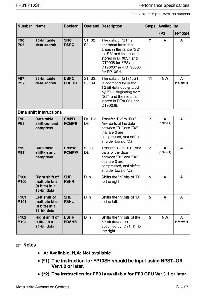
Performance SpecificationsFP3/FP10SH
G − 27Matsushita Automation Controls
G.2 Table of High-Level Instructions
Number Name Boolean Operand Description Steps Availability
FP3 FP10SH
F96P96
16-bit tabledata search
SRCPSRC
S1, S2,S3
The data of “S1” issearched for in theareas in the range “S2”to “S3” and the result isstored in DT9037 andDT9038 for FP3 andDT90037 and DT90038for FP10SH.
7 A A
F97P97
32-bit tabledata search
DSRCPDSRC
S1, S2,S3, S4
The data of (S1+1, S1)is searched for in the32-bit data designatedby “S3”, beginning from“S2”, and the result isstored in DT90037 andDT90038.
11 N/A A(* Note 1)
Data shift instructions
F98P98
Data tableshift-out andcompress
CMPRPCMPR
D1, D2,D3
Transfer “D2” to “D3.”Any parts of the databetween “D1” and “D2”that are 0 arecompressed, and shiftedin order toward “D2.”
7 A(* Note 2)
A
F99P99
Data tableshift-in andcompress
CMPWPCMPW
S, D1,D2
Transfer “S” to “D1”. Anyparts of the databetween “D1” and “D2”that are 0 arecompressed, and shiftedin order toward “D2.”
7 A(* Note 2)
A
F100P100
Right shift ofmultiple bits(n bits) in a16-bit data
SHRPSHR
D, n Shifts the “n” bits of “D”to the right.
5 A A
F101P101
Left shift ofmultiple bits(n bits) in a16-bit data
SHLPSHL
D, n Shifts the “n” bits of “D”to the left.
5 A A
F102P102
Right shift ofn bits in a32-bit data
DSHRPDSHR
D, n Shifts the “n” bits of the32-bit data areaspecified by (D+1, D) tothe right.
5 N/A A(* Note 1)
Notes
A: Available, N/A: Not available
(*1):The instruction for FP10SH should be input using NPST−GRVer.4.0 or later.
(*2):The instruction for FP3 is available for FP3 CPU Ver.3.1 or later.
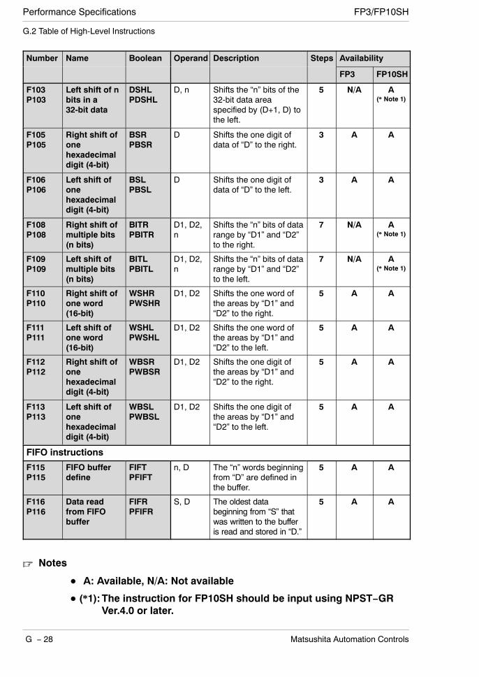
Performance Specifications FP3/FP10SH
G − 28 Matsushita Automation Controls
G.2 Table of High-Level Instructions
Number Name Boolean Operand Description Steps Availability
FP3 FP10SH
F103P103
Left shift of nbits in a32-bit data
DSHLPDSHL
D, n Shifts the “n” bits of the32-bit data areaspecified by (D+1, D) tothe left.
5 N/A A(* Note 1)
F105P105
Right shift ofonehexadecimaldigit (4-bit)
BSRPBSR
D Shifts the one digit ofdata of “D” to the right.
3 A A
F106P106
Left shift ofonehexadecimaldigit (4-bit)
BSLPBSL
D Shifts the one digit ofdata of “D” to the left.
3 A A
F108P108
Right shift ofmultiple bits(n bits)
BITRPBITR
D1, D2,n
Shifts the “n” bits of datarange by “D1” and “D2”to the right.
7 N/A A(* Note 1)
F109P109
Left shift ofmultiple bits(n bits)
BITLPBITL
D1, D2,n
Shifts the “n” bits of datarange by “D1” and “D2”to the left.
7 N/A A(* Note 1)
F110P110
Right shift ofone word(16-bit)
WSHRPWSHR
D1, D2 Shifts the one word ofthe areas by “D1” and“D2” to the right.
5 A A
F111P111
Left shift ofone word(16-bit)
WSHLPWSHL
D1, D2 Shifts the one word ofthe areas by “D1” and“D2” to the left.
5 A A
F112P112
Right shift ofonehexadecimaldigit (4-bit)
WBSRPWBSR
D1, D2 Shifts the one digit ofthe areas by “D1” and“D2” to the right.
5 A A
F113P113
Left shift ofonehexadecimaldigit (4-bit)
WBSLPWBSL
D1, D2 Shifts the one digit ofthe areas by “D1” and“D2” to the left.
5 A A
FIFO instructions
F115P115
FIFO bufferdefine
FIFTPFIFT
n, D The “n” words beginningfrom “D” are defined inthe buffer.
5 A A
F116P116
Data readfrom FIFObuffer
FIFRPFIFR
S, D The oldest databeginning from “S” thatwas written to the bufferis read and stored in “D.”
5 A A
Notes
A: Available, N/A: Not available
(*1):The instruction for FP10SH should be input using NPST−GRVer.4.0 or later.
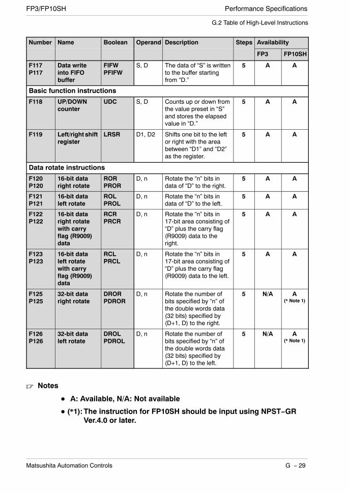
Performance SpecificationsFP3/FP10SH
G − 29Matsushita Automation Controls
G.2 Table of High-Level Instructions
Number Name Boolean Operand Description Steps Availability
FP3 FP10SH
F117P117
Data writeinto FIFObuffer
FIFWPFIFW
S, D The data of “S” is writtento the buffer startingfrom “D.”
5 A A
Basic function instructions
F118 UP/DOWNcounter
UDC S, D Counts up or down fromthe value preset in “S”and stores the elapsedvalue in “D.”
5 A A
F119 Left/right shiftregister
LRSR D1, D2 Shifts one bit to the leftor right with the areabetween “D1” and “D2”as the register.
5 A A
Data rotate instructions
F120P120
16-bit dataright rotate
RORPROR
D, n Rotate the “n” bits indata of “D” to the right.
5 A A
F121P121
16-bit dataleft rotate
ROLPROL
D, n Rotate the “n” bits indata of “D” to the left.
5 A A
F122P122
16-bit dataright rotatewith carryflag (R9009)data
RCRPRCR
D, n Rotate the “n” bits in17-bit area consisting of“D” plus the carry flag(R9009) data to theright.
5 A A
F123P123
16-bit dataleft rotatewith carryflag (R9009)data
RCLPRCL
D, n Rotate the “n” bits in17-bit area consisting of“D” plus the carry flag(R9009) data to the left.
5 A A
F125P125
32-bit dataright rotate
DRORPDROR
D, n Rotate the number ofbits specified by “n” ofthe double words data(32 bits) specified by(D+1, D) to the right.
5 N/A A(* Note 1)
F126P126
32-bit dataleft rotate
DROLPDROL
D, n Rotate the number ofbits specified by “n” ofthe double words data(32 bits) specified by(D+1, D) to the left.
5 N/A A(* Note 1)
Notes
A: Available, N/A: Not available
(*1):The instruction for FP10SH should be input using NPST−GRVer.4.0 or later.
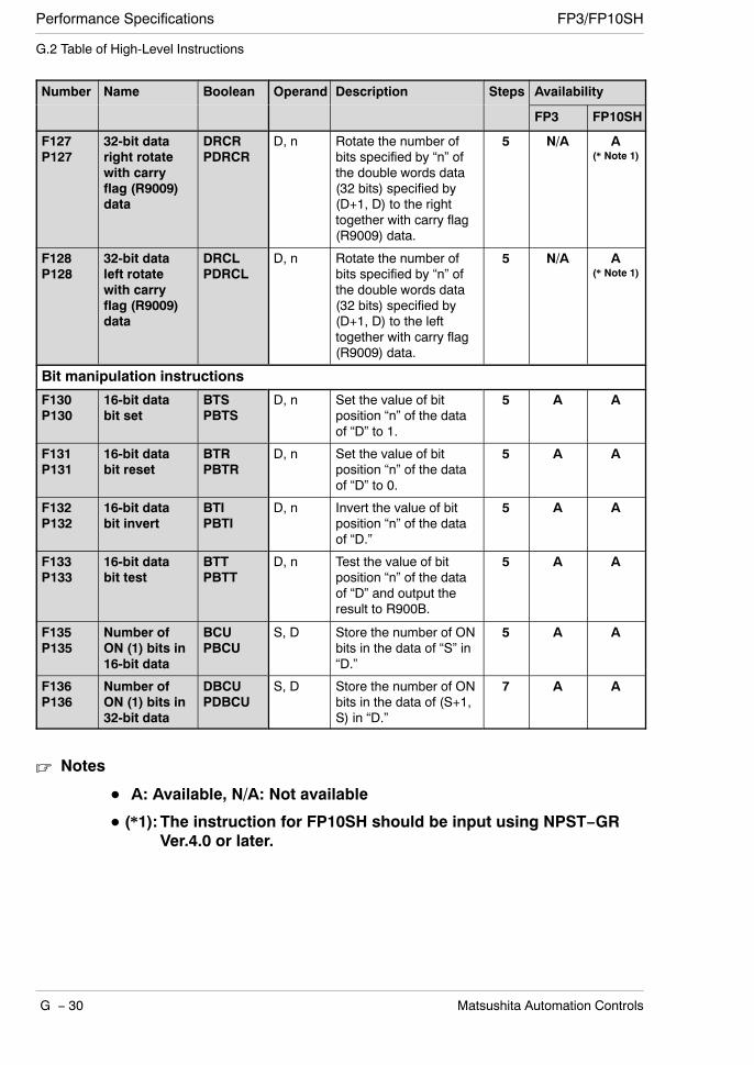
Performance Specifications FP3/FP10SH
G − 30 Matsushita Automation Controls
G.2 Table of High-Level Instructions
Number Name Boolean Operand Description Steps Availability
FP3 FP10SH
F127P127
32-bit dataright rotatewith carryflag (R9009)data
DRCRPDRCR
D, n Rotate the number ofbits specified by “n” ofthe double words data(32 bits) specified by(D+1, D) to the righttogether with carry flag(R9009) data.
5 N/A A(* Note 1)
F128P128
32-bit dataleft rotatewith carryflag (R9009)data
DRCLPDRCL
D, n Rotate the number ofbits specified by “n” ofthe double words data(32 bits) specified by(D+1, D) to the lefttogether with carry flag(R9009) data.
5 N/A A(* Note 1)
Bit manipulation instructions
F130P130
16-bit databit set
BTSPBTS
D, n Set the value of bitposition “n” of the dataof “D” to 1.
5 A A
F131P131
16-bit databit reset
BTRPBTR
D, n Set the value of bitposition “n” of the dataof “D” to 0.
5 A A
F132P132
16-bit databit invert
BTIPBTI
D, n Invert the value of bitposition “n” of the dataof “D.”
5 A A
F133P133
16-bit databit test
BTTPBTT
D, n Test the value of bitposition “n” of the dataof “D” and output theresult to R900B.
5 A A
F135P135
Number ofON (1) bits in16-bit data
BCUPBCU
S, D Store the number of ONbits in the data of “S” in“D.”
5 A A
F136P136
Number ofON (1) bits in32-bit data
DBCUPDBCU
S, D Store the number of ONbits in the data of (S+1,S) in “D.”
7 A A
Notes
A: Available, N/A: Not available
(*1):The instruction for FP10SH should be input using NPST−GRVer.4.0 or later.
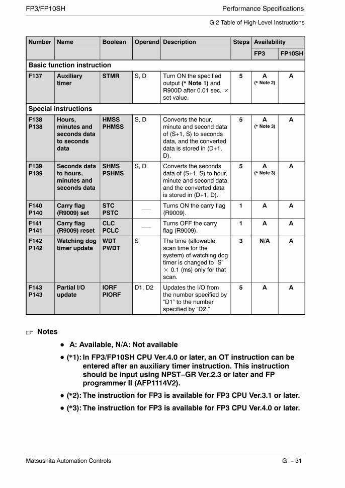
Performance SpecificationsFP3/FP10SH
G − 31Matsushita Automation Controls
G.2 Table of High-Level Instructions
Number Name Boolean Operand Description Steps Availability
FP3 FP10SH
Basic function instruction
F137 Auxiliarytimer
STMR S, D Turn ON the specifiedoutput (* Note 1) andR900D after 0.01 sec.×set value.
5 A(* Note 2)
A
Special instructions
F138P138
Hours,minutes andseconds datato secondsdata
HMSSPHMSS
S, D Converts the hour,minute and second dataof (S+1, S) to secondsdata, and the converteddata is stored in (D+1,D).
5 A(* Note 3)
A
F139P139
Seconds datato hours,minutes andseconds data
SHMSPSHMS
S, D Converts the secondsdata of (S+1, S) to hour,minute and second data,and the converted datais stored in (D+1, D).
5 A(* Note 3)
A
F140P140
Carry flag(R9009) set
STCPSTC
Turns ON the carry flag(R9009).
1 A A
F141P141
Carry flag(R9009) reset
CLCPCLC
Turns OFF the carryflag (R9009).
1 A A
F142P142
Watching dogtimer update
WDTPWDT
S The time (allowablescan time for thesystem) of watching dogtimer is changed to “S”× 0.1 (ms) only for thatscan.
3 N/A A
F143P143
Partial I/Oupdate
IORFPIORF
D1, D2 Updates the I/O fromthe number specified by“D1” to the numberspecified by “D2.”
5 A A
Notes
A: Available, N/A: Not available
(*1): In FP3/FP10SH CPU Ver.4.0 or later, an OT instruction can beentered after an auxiliary timer instruction. This instructionshould be input using NPST−GR Ver.2.3 or later and FPprogrammer II (AFP1114V2).
(*2):The instruction for FP3 is available for FP3 CPU Ver.3.1 or later.
(*3):The instruction for FP3 is available for FP3 CPU Ver.4.0 or later.
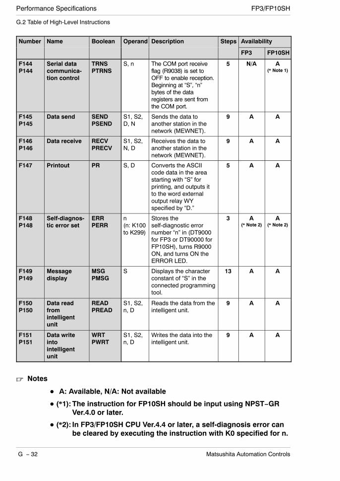
Performance Specifications FP3/FP10SH
G − 32 Matsushita Automation Controls
G.2 Table of High-Level Instructions
Number Name Boolean Operand Description Steps Availability
FP3 FP10SH
F144P144
Serial datacommunica-tion control
TRNSPTRNS
S, n The COM port receiveflag (R9038) is set toOFF to enable reception.Beginning at “S”, “n”bytes of the dataregisters are sent fromthe COM port.
5 N/A A(* Note 1)
F145P145
Data send SENDPSEND
S1, S2,D, N
Sends the data toanother station in thenetwork (MEWNET).
9 A A
F146P146
Data receive RECVPRECV
S1, S2,N, D
Receives the data toanother station in thenetwork (MEWNET).
9 A A
F147 Printout PR S, D Converts the ASCIIcode data in the areastarting with “S” forprinting, and outputs itto the word externaloutput relay WYspecified by “D.”
5 A A
F148P148
Self-diagnos-tic error set
ERRPERR
n(n: K100to K299)
Stores theself-diagnostic errornumber “n” in (DT9000for FP3 or DT90000 forFP10SH), turns R9000ON, and turns ON theERROR LED.
3 A(* Note 2)
A(* Note 2)
F149P149
Messagedisplay
MSGPMSG
S Displays the characterconstant of “S” in theconnected programmingtool.
13 A A
F150P150
Data readfromintelligentunit
READPREAD
S1, S2,n, D
Reads the data from theintelligent unit.
9 A A
F151P151
Data writeintointelligentunit
WRTPWRT
S1, S2,n, D
Writes the data into theintelligent unit.
9 A A
Notes
A: Available, N/A: Not available
(*1):The instruction for FP10SH should be input using NPST−GRVer.4.0 or later.
(*2): In FP3/FP10SH CPU Ver.4.4 or later, a self-diagnosis error canbe cleared by executing the instruction with K0 specified for n.

Performance SpecificationsFP3/FP10SH
G − 33Matsushita Automation Controls
G.2 Table of High-Level Instructions
Number Name Boolean Operand Description Steps Availability
FP3 FP10SH
F152P152
Data readfromMEWNET-Fslave station
RMRDPRMRD
S1, S2,n, D
Reads the data from theintelligent unit at theMEWNET-F (remoteI/O) slave station.
9 A A
F153P153
Data writeintoMEWNET-Fslave station
RMWTPRMWT
S1, S2,n, D
Writes the data into theintelligent unit at theMEWNET-F (remoteI/O) slave station.
9 A A
F154P154
Machinelanguageprogram call
MCALPMCAL
n The machine languageprogram is called.
3 A N/A
F155P155
Sampling SMPLPSMPL
Starts sampling data. 1 A A
F156P156
Samplingtrigger
STRGPSTRG
When the trigger of thisinstruction turns ON, thesampling trace stops.
1 A A
F157P157
Time addition CADDPCADD
S1, S2,D
The time after (S2+1,S2) elapses from thetime of (S1+2, S1+1,S1) is stored in (D+2,D+1, D).
9 A A
F158P158
Timesubstruction
CSUBPCSUB
S1, S2,D
The time that resultsfrom subtracting (S2+1,S2) from the time(S1+2, S1+1, S1) isstored in (D+2, D+1, D).
9 A A
BIN arithmetic instruction
F160P160
Double word(32-bit) datasquare root
DSQRPDSQR
S, D √(S)→ (D) 7 A A
Basic function instruction
F183 Auxiliarytimer (32-bit)
DSTM S, D Turn ON the specifiedoutput and R900D after0.01 sec.× set value.
7 N/A A(* Note 1)
Notes
A: Available, N/A: Not available
(*1):The instruction for FP10SH is available for FP10SH CPUVer.3.1 or later and this instruction for FP10SH should be inputusing NPST−GR Ver.4.0 or later.
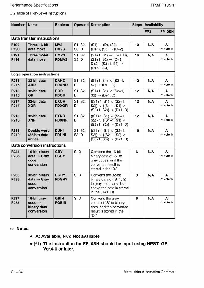
Performance Specifications FP3/FP10SH
G − 34 Matsushita Automation Controls
G.2 Table of High-Level Instructions
Number Name Boolean Operand Description Steps Availability
FP3 FP10SH
Data transfer instructions
F190P190
Three 16-bitdata move
MV3PMV3
S1, S2,S3, D
(S1)→ (D), (S2)→(D+1), (S3)→ (D+2)
10 N/A A(* Note 1)
F191P191
Three 32-bitdata move
DMV3PDMV3
S1, S2,S3, D
(S1+1, S1)→ (D+1, D),(S2+1, S2)→ (D+3,D+2), (S3+1, S3)→(D+5, D+4)
16 N/A A(* Note 1)
Logic operation instructions
F215P215
32-bit dataAND
DANDPDAND
S1, S2,D
(S1+1, S1)∧ (S2+1,S2)→ (D+1, D)
12 N/A A(* Note 1)
F216P216
32-bit dataOR
DORPDOR
S1, S2,D
(S1+1, S1)∨ (S2+1,S2)→ (D+1, D)
12 N/A A(* Note 1)
F217P217
32-bit dataXOR
DXORPDXOR
S1, S2,D
(S1+1, S1)∧ (S2+1,S2)∨ (S1+1, S1)∧(S2+1, S2)→ (D+1, D)
12 N/A A(* Note 1)
F218P218
32-bit dataXNR
DXNRPDXNR
S1, S2,D
(S1+1, S1)∧ (S2+1,S2)∨ (S1+1, S1)∧(S2+1, S2)→ (D+1, D)
12 N/A A(* Note 1)
F219P219
Double word(32-bit) dataunites
DUNIPDUNI
S1, S2,S3, D
(S1+1, S1)∧ (S3+1,S3)∨ (S2+1, S2)∧(S3+1, S3)→ (D+1, D)
16 N/A A(* Note 1)
Data conversion instructions
F235P235
16-bit binarydata→ Graycodeconversion
GRYPGRY
S, D Converts the 16-bitbinary data of “S” togray codes, and theconverted result isstored in the “D.”
6 N/A A(* Note 1)
F236P236
32-bit binarydata→ Graycodeconversion
DGRYPDGRY
S, D Converts the 32-bitbinary data of (S+1, S)to gray code, and theconverted data is storedin the (D+1, D).
8 N/A A(* Note 1)
F237P237
16-bit graycode→binary dataconversion
GBINPGBIN
S, D Converts the graycodes of “S” to binarydata, and the convertedresult is stored in the“D.”
6 N/A A(* Note 1)
Notes
A: Available, N/A: Not available
(*1):The instruction for FP10SH should be input using NPST−GRVer.4.0 or later.

Performance SpecificationsFP3/FP10SH
G − 35Matsushita Automation Controls
G.2 Table of High-Level Instructions
Number Name Boolean Operand Description Steps Availability
FP3 FP10SH
F238P238
32-bit graycode→binary dataconversion
DGBINPDGBIN
S, D Converts the gray codeof (S+1, S) to binarydata,and the convertedresult is stored in the(D+1, D).
8 N/A A(* Note 1)
F240P240
Bit line to bitcolumnconversion
COLMPCOLM
S1, S2,D
The values of bits 0 to15 of “S” are stored inbit “n” of (D to D+15).
8 N/A A(* Note 1)
F241P241
Bit column tobit lineconversion
LINEPLINE
S1, S2,D
The values of bit “n” of(S to S+15) are storedin bits 0 to 15 of “D.”
8 N/A A(* Note 1)
Integer type data processing instructions
F270P270
Maximumvalue (worddata (16-bit))
MAXPMAX
S1, S2,D
Searches the maximumvalue in the word datatable between the “S1”and “S2”, and stores itin the “D.” The addressrelative to “S1” is storedin “D+1.”
8 N/A A(* Note 1)
F271P271
Maximumvalue (doubleword data(32-bit))
DMAXPDMAX
S1, S2,D
Searches for themaximum value in thedouble word data tablebetween the areaselected with “S1” and“S2”, and stores it in the“D.” The addressrelative to “S1” is storedin “D+2.”
8 N/A A(* Note 1)
F272P272
Minimumvalue (worddata (16-bit))
MINPMIN
S1, S2,D
Searches for theminimum value in theword data tablebetween the areaselected with “S1” and“S2”, and stores it in the“D.” The addressrelative to “S1” is storedin “D+1.”
8 N/A A(* Note 1)
Notes
A: Available, N/A: Not available
(*1):The instruction for FP10SH should be input using NPST−GRVer.4.0 or later.
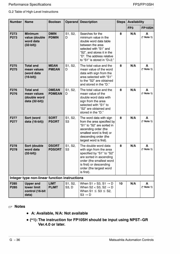
Performance Specifications FP3/FP10SH
G − 36 Matsushita Automation Controls
G.2 Table of High-Level Instructions
Number Name Boolean Operand Description Steps Availability
FP3 FP10SH
F273P273
Minimumvalue (doubleword data(32-bit))
DMINPDMIN
S1, S2,D
Searches for theminimum value in thedouble word data tablebetween the areaselected with “S1” and“S2”, and stores it in the“D”. The address relativeto “S1” is stored in “D+2.”
8 N/A A(* Note 1)
F275P275
Total andmean values(word data(16-bit))
MEANPMEAN
S1, S2,D
The total value and themean value of the worddata with sign from thearea selected with “S1”to the “S2” are obtainedand stored in the “D.”
8 N/A A(* Note 1)
F276P276
Total andmean values(double worddata (32-bit))
DMEANPDMEAN
S1, S2,D
The total value and themean value of thedouble word data withsign from the areaselected with “S1” to“S2” are obtained andstored in the “D.”
8 N/A A(* Note 1)
F277P277
Sort (worddata (16-bit))
SORTPSORT
S1, S2,S3
The word data with signfrom the area specified by“S1” to “S2” are sorted inascending order (thesmallest word is first) ordescending order (thelargest word is first).
8 N/A A(* Note 1)
F278P278
Sort (doubleword data(32-bit))
DSORTPDSORT
S1, S2,S3
The double word datawith sign from the areaspecified by “S1” to “S2”are sorted in ascendingorder (the smallest wordis first) or descendingorder (the largest wordis first).
8 N/A A(* Note 1)
Integer type non-linear function instructions
F285P285
Upper andlower limitcontrol (16-bitdata)
LIMTPLIMT
S1, S2,S3, D
When S1 > S3, S1→ DWhen S2 < S3, S2→ DWhen S1≦ S3≦ S2,S3→ D
10 N/A A(* Note 1)
Notes
A: Available, N/A: Not available
(*1):The instruction for FP10SH should be input using NPST−GRVer.4.0 or later.

Performance SpecificationsFP3/FP10SH
G − 37Matsushita Automation Controls
G.2 Table of High-Level Instructions
Number Name Boolean Operand Description Steps Availability
FP3 FP10SH
F286P286
Upper andlower limitcontrol (32-bitdata)
DLIMTPDLIMT
S1, S2,S3, D
When (S1+1, S1) >(S3+1, S3), (S1+1, S1)→ (D+1, D)When (S2+1, S2) <(S3+1, S3), (S2+1, S2)→ (D+1, D)When (S1+1, S1)≦(S3+1, S3)≦ (S2+1,S2), (S3+1, S3)→(D+1, D)
16 N/A A(* Note 1)
F287P287
Deadbandcontrol (16-bitdata)
BANDPBAND
S1, S2,S3, D
When S1 > S3, S3 − S1→ DWhen S2 < S3, S3 − S2→ DWhen S1≦ S3≦ S2, 0→ D
10 N/A A(* Note 1)
F288P288
Deadbandcontrol (32-bitdata)
DBANDPDBAND
S1, S2,S3, D
When (S1+1, S1) >(S3+1, S3), (S3+1, S3) −(S1+1, S1)→ (D+1, D)When (S2+1, S2) <(S3+1, S3), (S3+1, S3) −(S2+1, S2)→ (D+1, D)When (S1+1, S1)≦(S3+1, S3)≦ (S2+1,S2), 0→ (D+1, D)
16 N/A A(* Note 1)
F289P289
Zone control(16-bit data)
ZONEPZONE
S1, S2,S3, D
When S3 < 0, S3 + S1→ DWhen S3 = 0, 0→ DWhen S3 > 0, S3 + S2→ D
10 N/A A(* Note 1)
F290P290
Zone control(32-bit data)
DZONEPDZONE
S1, S2,S3, D
When (S3+1, S3) < 0,(S3+1, S3) + (S1+1, S1)→ (D+1, D)When (S3+1, S3) = 0, 0→ (D+1, D)When (S3+1, S3) > 0,(S3+1, S3) + (S2+1, S2)→ (D+1, D)
16 N/A A(* Note 1)
Notes
A: Available, N/A: Not available
(*1):The instruction for FP10SH should be input using NPST−GRVer.4.0 or later.

Performance Specifications FP3/FP10SH
G − 38 Matsushita Automation Controls
G.2 Table of High-Level Instructions
Number Name Boolean Operand Description Steps Availability
FP3 FP10SH
BCD type real number operation instructions
F300P300
BCD typesineoperation
BSINPBSIN
S, D SIN (S+1, S)→(D+1, D)
6 N/A A(* Note 1)
F301P301
BCD typecosineoperation
BCOSPBCOS
S, D COS (S+1, S)→(D+1, D)
6 N/A A(* Note 1)
F302P302
BCD typetangentoperation
BTANPBTAN
S, D TAN (S+1, S)→(D+1, D)
6 N/A A(* Note 1)
F303P303
BCD typearcsineoperation
BASINPBASIN
S, D SIN−1 (S+1, S)→(D+1, D)
6 N/A A(* Note 1)
F304P304
BCD typearccosineoperation
BACOSPBACOS
S, D COS−1 (S+1, S)→(D+1, D)
6 N/A A(* Note 1)
F305P305
BCD typearctangentoperation
BATANPBATAN
S, D TAN−1 (S+1, S)→(D+1, D)
6 N/A A(* Note 1)
Floating-point type real number operation instructions
F309P309
Floating-pointtype real datamove
FMVPFMV
S, D (S+1, S)→ (D+1, D) 8 N/A A(* Note 1)
F310P310
Floating-pointtype real dataaddition
F+PF+
S1, S2,D
( S1+1, S1) + (S2+1,S2)→ ( D+1, D)
14 N/A A(* Note 1)
F311P311
Floating-pointtype real datasubtraction
F−PF−
S1, S2,D
( S1+1, S1) − (S2+1,S2)→ ( D+1, D)
14 N/A A(* Note 1)
F312P312
Floating-pointtype real datamultiplication
F*PF*
S1, S2,D
( S1+1, S1)× (S2+1,S2)→ ( D+1, D)
14 N/A A(* Note 1)
F313P313
Floating-pointtype real datadivision
F%PF%
S1, S2,D
( S1+1, S1)÷ (S2+1,S2)→ ( D+1, D)
14 N/A A(* Note 1)
F314P314
Floating-pointtype real datasineoperation
SINPSIN
S, D SIN (S+1, S)→(D+1, D)
10 N/A A(* Note 1)
Notes
A: Available, N/A: Not available
(*1):The instruction for FP10SH should be input using NPST−GRVer.4.0 or later.
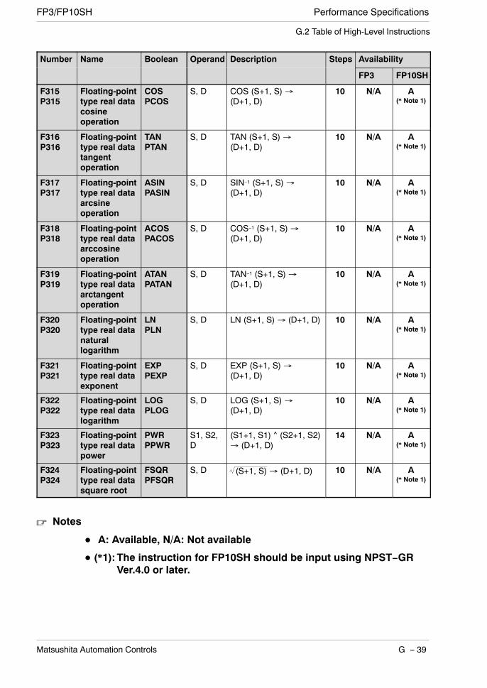
Performance SpecificationsFP3/FP10SH
G − 39Matsushita Automation Controls
G.2 Table of High-Level Instructions
Number Name Boolean Operand Description Steps Availability
FP3 FP10SH
F315P315
Floating-pointtype real datacosineoperation
COSPCOS
S, D COS (S+1, S)→(D+1, D)
10 N/A A(* Note 1)
F316P316
Floating-pointtype real datatangentoperation
TANPTAN
S, D TAN (S+1, S)→(D+1, D)
10 N/A A(* Note 1)
F317P317
Floating-pointtype real dataarcsineoperation
ASINPASIN
S, D SIN−1 (S+1, S)→(D+1, D)
10 N/A A(* Note 1)
F318P318
Floating-pointtype real dataarccosineoperation
ACOSPACOS
S, D COS−1 (S+1, S)→(D+1, D)
10 N/A A(* Note 1)
F319P319
Floating-pointtype real dataarctangentoperation
ATANPATAN
S, D TAN−1 (S+1, S)→(D+1, D)
10 N/A A(* Note 1)
F320P320
Floating-pointtype real datanaturallogarithm
LNPLN
S, D LN (S+1, S)→ (D+1, D) 10 N/A A(* Note 1)
F321P321
Floating-pointtype real dataexponent
EXPPEXP
S, D EXP (S+1, S)→(D+1, D)
10 N/A A(* Note 1)
F322P322
Floating-pointtype real datalogarithm
LOGPLOG
S, D LOG (S+1, S)→(D+1, D)
10 N/A A(* Note 1)
F323P323
Floating-pointtype real datapower
PWRPPWR
S1, S2,D
(S1+1, S1) ^ (S2+1, S2)→ (D+1, D)
14 N/A A(* Note 1)
F324P324
Floating-pointtype real datasquare root
FSQRPFSQR
S, D (S+1, S)→ (D+1, D) 10 N/A A(* Note 1)
Notes
A: Available, N/A: Not available
(*1):The instruction for FP10SH should be input using NPST−GRVer.4.0 or later.
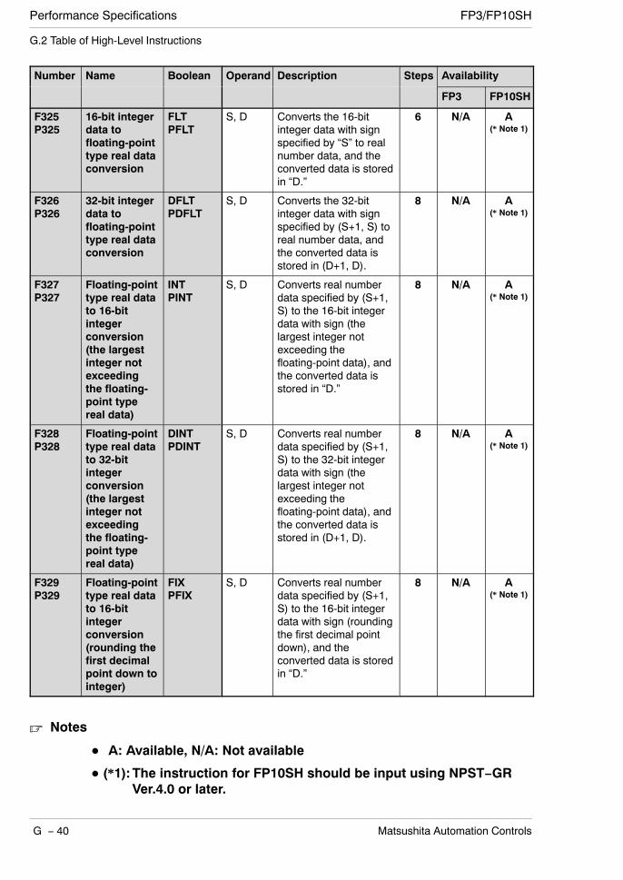
Performance Specifications FP3/FP10SH
G − 40 Matsushita Automation Controls
G.2 Table of High-Level Instructions
Number Name Boolean Operand Description Steps Availability
FP3 FP10SH
F325P325
16-bit integerdata tofloating-pointtype real dataconversion
FLTPFLT
S, D Converts the 16-bitinteger data with signspecified by “S” to realnumber data, and theconverted data is storedin “D.”
6 N/A A(* Note 1)
F326P326
32-bit integerdata tofloating-pointtype real dataconversion
DFLTPDFLT
S, D Converts the 32-bitinteger data with signspecified by (S+1, S) toreal number data, andthe converted data isstored in (D+1, D).
8 N/A A(* Note 1)
F327P327
Floating-pointtype real datato 16-bitintegerconversion(the largestinteger notexceedingthe floating-point typereal data)
INTPINT
S, D Converts real numberdata specified by (S+1,S) to the 16-bit integerdata with sign (thelargest integer notexceeding thefloating-point data), andthe converted data isstored in “D.”
8 N/A A(* Note 1)
F328P328
Floating-pointtype real datato 32-bitintegerconversion(the largestinteger notexceedingthe floating-point typereal data)
DINTPDINT
S, D Converts real numberdata specified by (S+1,S) to the 32-bit integerdata with sign (thelargest integer notexceeding thefloating-point data), andthe converted data isstored in (D+1, D).
8 N/A A(* Note 1)
F329P329
Floating-pointtype real datato 16-bitintegerconversion(rounding thefirst decimalpoint down tointeger)
FIXPFIX
S, D Converts real numberdata specified by (S+1,S) to the 16-bit integerdata with sign (roundingthe first decimal pointdown), and theconverted data is storedin “D.”
8 N/A A(* Note 1)
Notes
A: Available, N/A: Not available
(*1):The instruction for FP10SH should be input using NPST−GRVer.4.0 or later.

Performance SpecificationsFP3/FP10SH
G − 41Matsushita Automation Controls
G.2 Table of High-Level Instructions
Number Name Boolean Operand Description Steps Availability
FP3 FP10SH
F330P330
Floating-pointtype real datato 32-bitintegerconversion(rounding thefirst decimalpoint down tointeger)
DFIXPDFIX
S, D Converts real numberdata specified by (S+1,S) to the 32-bit integerdata with sign (roundingthe first decimal pointdown), and theconverted data is storedin (D+1, D).
8 N/A A(* Note 1)
F331P331
Floating-pointtype real datato 16-bitintegerconversion(rounding thefirst decimalpoint off tointeger)
ROFFPROFF
S, D Converts real numberdata specified by (S+1,S) to the 16-bit integerdata with sign (roundingthe first decimal pointoff), and the converteddata is stored in “D.”
8 N/A A(* Note 1)
F332P332
Floating-pointtype real datato 32-bitintegerconversion(rounding thefirst decimalpoint off tointeger)
DROFFPDROFF
S, D Converts real numberdata specified by (S+1,S) to the 32-bit integerdata with sign(roundingthe first decimal pointoff), and the converteddata is stored in (D+1,D).
8 N/A A(* Note 1)
F333P333
Floating-pointtype real datarounding thefirst decimalpoint down
FINTPFINT
S, D The decimal part of thereal number dataspecified in (S+1, S) isrounded down, and theresult is stored in (D+1,D).
8 N/A A(* Note 1)
F334P334
Floating-pointtype real datarounding thefirst decimalpoint off
FRINTPFRINT
S, D The decimal part of thereal number data storedin (S+1, S) is roundedoff, and the result isstored in (D+1, D).
8 N/A A(* Note 1)
F335P335
Floating-pointtype real datasign changes
F+/−PF+/−
S, D The real number datastored in (S+1, S) ischanged the sign, andthe result is stored in(D+1, D).
8 N/A A(* Note 1)
Notes
A: Available, N/A: Not available
(*1):The instruction for FP10SH should be input using NPST−GRVer.4.0 or later.
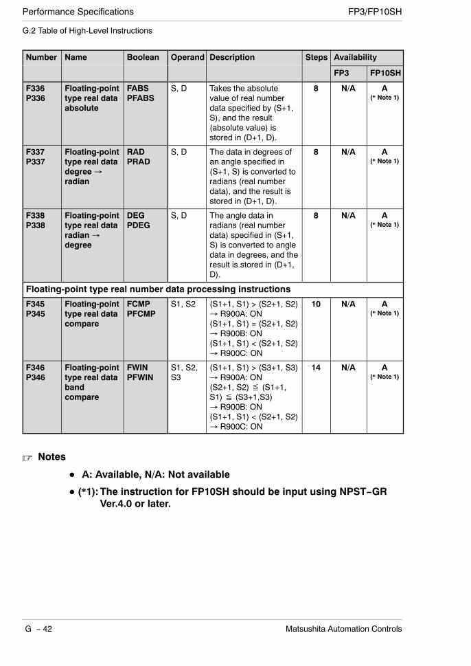
Performance Specifications FP3/FP10SH
G − 42 Matsushita Automation Controls
G.2 Table of High-Level Instructions
Number Name Boolean Operand Description Steps Availability
FP3 FP10SH
F336P336
Floating-pointtype real dataabsolute
FABSPFABS
S, D Takes the absolutevalue of real numberdata specified by (S+1,S), and the result(absolute value) isstored in (D+1, D).
8 N/A A(* Note 1)
F337P337
Floating-pointtype real datadegree→radian
RADPRAD
S, D The data in degrees ofan angle specified in(S+1, S) is converted toradians (real numberdata), and the result isstored in (D+1, D).
8 N/A A(* Note 1)
F338P338
Floating-pointtype real dataradian→degree
DEGPDEG
S, D The angle data inradians (real numberdata) specified in (S+1,S) is converted to angledata in degrees, and theresult is stored in (D+1,D).
8 N/A A(* Note 1)
Floating-point type real number data processing instructions
F345P345
Floating-pointtype real datacompare
FCMPPFCMP
S1, S2 (S1+1, S1) > (S2+1, S2)→ R900A: ON(S1+1, S1) = (S2+1, S2)→ R900B: ON(S1+1, S1) < (S2+1, S2)→ R900C: ON
10 N/A A(* Note 1)
F346P346
Floating-pointtype real databandcompare
FWINPFWIN
S1, S2,S3
(S1+1, S1) > (S3+1, S3)→ R900A: ON(S2+1, S2)≦ (S1+1,S1)≦ (S3+1,S3)→ R900B: ON(S1+1, S1) < (S2+1, S2)→ R900C: ON
14 N/A A(* Note 1)
Notes
A: Available, N/A: Not available
(*1):The instruction for FP10SH should be input using NPST−GRVer.4.0 or later.
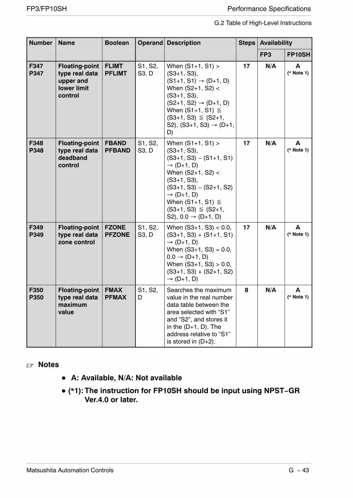
Performance SpecificationsFP3/FP10SH
G − 43Matsushita Automation Controls
G.2 Table of High-Level Instructions
Number Name Boolean Operand Description Steps Availability
FP3 FP10SH
F347P347
Floating-pointtype real dataupper andlower limitcontrol
FLIMTPFLIMT
S1, S2,S3, D
When (S1+1, S1) >(S3+1, S3),(S1+1, S1)→ (D+1, D)When (S2+1, S2) <(S3+1, S3),(S2+1, S2)→ (D+1, D)When (S1+1, S1)≦(S3+1, S3)≦ (S2+1,S2), (S3+1, S3)→ (D+1,D)
17 N/A A(* Note 1)
F348P348
Floating-pointtype real datadeadbandcontrol
FBANDPFBAND
S1, S2,S3, D
When (S1+1, S1) >(S3+1, S3),(S3+1, S3) − (S1+1, S1)→ (D+1, D)When (S2+1, S2) <(S3+1, S3),(S3+1, S3) − (S2+1, S2)→ (D+1, D)When (S1+1, S1)≦(S3+1, S3)≦ (S2+1,S2), 0.0→ (D+1, D)
17 N/A A(* Note 1)
F349P349
Floating-pointtype real datazone control
FZONEPFZONE
S1, S2,S3, D
When (S3+1, S3) < 0.0,(S3+1, S3) + (S1+1, S1)→ (D+1, D)When (S3+1, S3) = 0.0,0.0→ (D+1, D)When (S3+1, S3) > 0.0,(S3+1, S3) + (S2+1, S2)→ (D+1, D)
17 N/A A(* Note 1)
F350P350
Floating-pointtype real datamaximumvalue
FMAXPFMAX
S1, S2,D
Searches the maximumvalue in the real numberdata table between thearea selected with “S1”and “S2”, and stores itin the (D+1, D). Theaddress relative to “S1”is stored in (D+2).
8 N/A A(* Note 1)
Notes
A: Available, N/A: Not available
(*1):The instruction for FP10SH should be input using NPST−GRVer.4.0 or later.
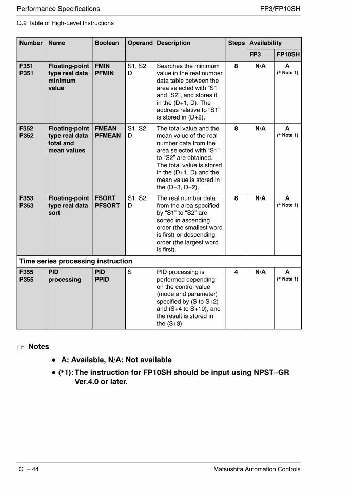
Performance Specifications FP3/FP10SH
G − 44 Matsushita Automation Controls
G.2 Table of High-Level Instructions
Number Name Boolean Operand Description Steps Availability
FP3 FP10SH
F351P351
Floating-pointtype real dataminimumvalue
FMINPFMIN
S1, S2,D
Searches the minimumvalue in the real numberdata table between thearea selected with “S1”and “S2”, and stores itin the (D+1, D). Theaddress relative to “S1”is stored in (D+2).
8 N/A A(* Note 1)
F352P352
Floating-pointtype real datatotal andmean values
FMEANPFMEAN
S1, S2,D
The total value and themean value of the realnumber data from thearea selected with “S1”to “S2” are obtained.The total value is storedin the (D+1, D) and themean value is stored inthe (D+3, D+2).
8 N/A A(* Note 1)
F353P353
Floating-pointtype real datasort
FSORTPFSORT
S1, S2,D
The real number datafrom the area specifiedby “S1” to “S2” aresorted in ascendingorder (the smallest wordis first) or descendingorder (the largest wordis first).
8 N/A A(* Note 1)
Time series processing instruction
F355P355
PIDprocessing
PIDPPID
S PID processing isperformed dependingon the control value(mode and parameter)specified by (S to S+2)and (S+4 to S+10), andthe result is stored inthe (S+3).
4 N/A A(* Note 1)
Notes
A: Available, N/A: Not available
(*1):The instruction for FP10SH should be input using NPST−GRVer.4.0 or later.
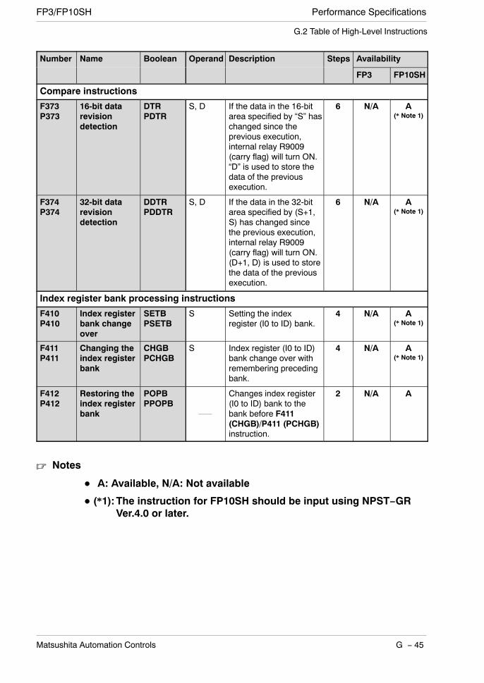
Performance SpecificationsFP3/FP10SH
G − 45Matsushita Automation Controls
G.2 Table of High-Level Instructions
Number Name Boolean Operand Description Steps Availability
FP3 FP10SH
Compare instructions
F373P373
16-bit datarevisiondetection
DTRPDTR
S, D If the data in the 16-bitarea specified by “S” haschanged since theprevious execution,internal relay R9009(carry flag) will turn ON.“D” is used to store thedata of the previousexecution.
6 N/A A(* Note 1)
F374P374
32-bit datarevisiondetection
DDTRPDDTR
S, D If the data in the 32-bitarea specified by (S+1,S) has changed sincethe previous execution,internal relay R9009(carry flag) will turn ON.(D+1, D) is used to storethe data of the previousexecution.
6 N/A A(* Note 1)
Index register bank processing instructions
F410P410
Index registerbank changeover
SETBPSETB
S Setting the indexregister (I0 to ID) bank.
4 N/A A(* Note 1)
F411P411
Changing theindex registerbank
CHGBPCHGB
S Index register (I0 to ID)bank change over withremembering precedingbank.
4 N/A A(* Note 1)
F412P412
Restoring theindex registerbank
POPBPPOPB
Changes index register(I0 to ID) bank to thebank before F411(CHGB)/P411 (PCHGB)instruction.
2 N/A A
Notes
A: Available, N/A: Not available
(*1):The instruction for FP10SH should be input using NPST−GRVer.4.0 or later.

Performance Specifications FP3/FP10SH
G − 46 Matsushita Automation Controls
G.2 Table of High-Level Instructions

Appendix H
Table of Binary/Hexadecimal/BCDExpressions

Table of Binary/Hexadecimal/BCD Expressions FP3/FP10SH
H − 2 Matsushita Automation Controls
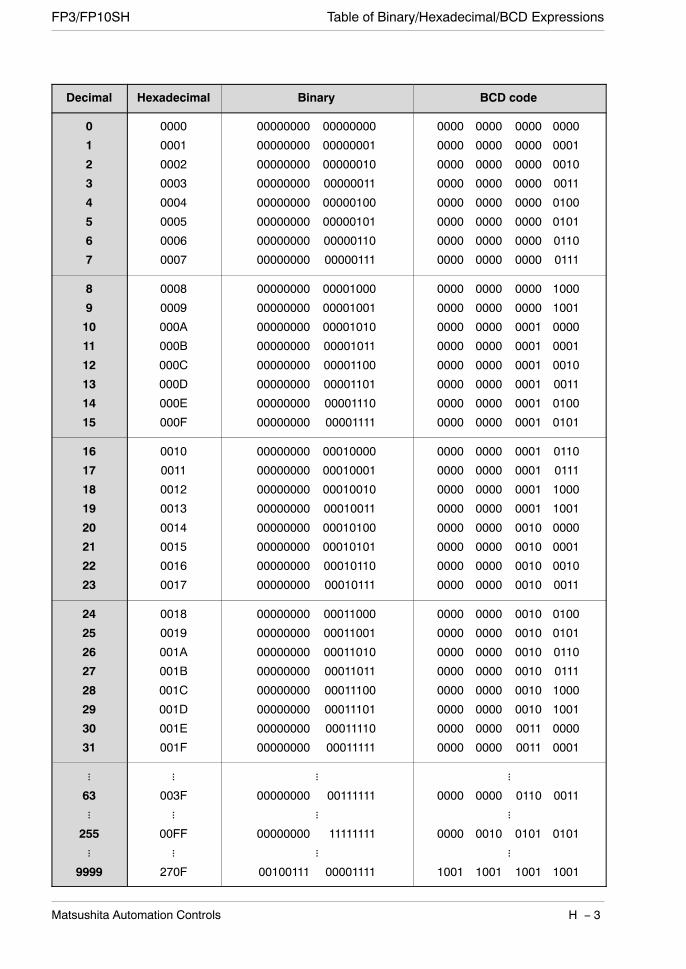
Table of Binary/Hexadecimal/BCD ExpressionsFP3/FP10SH
H − 3Matsushita Automation Controls
Decimal Hexadecimal Binary BCD code
0
1
2
3
4
5
6
7
0000
0001
0002
0003
0004
0005
0006
0007
00000000 00000000
00000000 00000001
00000000 00000010
00000000 00000011
00000000 00000100
00000000 00000101
00000000 00000110
00000000 00000111
0000 0000 0000 0000
0000 0000 0000 0001
0000 0000 0000 0010
0000 0000 0000 0011
0000 0000 0000 0100
0000 0000 0000 0101
0000 0000 0000 0110
0000 0000 0000 0111
8
9
10
11
12
13
14
15
0008
0009
000A
000B
000C
000D
000E
000F
00000000 00001000
00000000 00001001
00000000 00001010
00000000 00001011
00000000 00001100
00000000 00001101
00000000 00001110
00000000 00001111
0000 0000 0000 1000
0000 0000 0000 1001
0000 0000 0001 0000
0000 0000 0001 0001
0000 0000 0001 0010
0000 0000 0001 0011
0000 0000 0001 0100
0000 0000 0001 0101
16
17
18
19
20
21
22
23
0010
0011
0012
0013
0014
0015
0016
0017
00000000 00010000
00000000 00010001
00000000 00010010
00000000 00010011
00000000 00010100
00000000 00010101
00000000 00010110
00000000 00010111
0000 0000 0001 0110
0000 0000 0001 0111
0000 0000 0001 1000
0000 0000 0001 1001
0000 0000 0010 0000
0000 0000 0010 0001
0000 0000 0010 0010
0000 0000 0010 0011
24
25
26
27
28
29
30
31
0018
0019
001A
001B
001C
001D
001E
001F
00000000 00011000
00000000 00011001
00000000 00011010
00000000 00011011
00000000 00011100
00000000 00011101
00000000 00011110
00000000 00011111
0000 0000 0010 0100
0000 0000 0010 0101
0000 0000 0010 0110
0000 0000 0010 0111
0000 0000 0010 1000
0000 0000 0010 1001
0000 0000 0011 0000
0000 0000 0011 0001
⋮63
⋮255
⋮9999
⋮003F
⋮00FF
⋮270F
⋮00000000 00111111
⋮00000000 11111111
⋮00100111 00001111
⋮0000 0000 0110 0011
⋮0000 0010 0101 0101
⋮1001 1001 1001 1001

Table of Binary/Hexadecimal/BCD Expressions FP3/FP10SH
H − 4 Matsushita Automation Controls

Appendix I
ASCII Codes

ASCII Codes FP3/FP10SH
I − 2 Matsushita Automation Controls

ASCII CodesFP3/FP10SH
I − 3Matsushita Automation Controls
b6 0 0 0 0 1 1 1 1
b5 0 0 1 1 0 0 1 1
b4 0 1 0 1 0 1 0 1
b6 b5 b4 b3 b2 b1 b0ASCII
Most significant digitb6 b5 b4 b3 b2 b1 b0
ASCIIHEX code
0 1 2 3 4 5 6 7
0 0 0 0 0 NUL DEL SPACE 0 @ P ` p
0 0 0 1 1 SOH DC1 ! 1 A Q a q
0 0 1 0 2 STX DC2 〃 2 B R b r
0 0 1 1 3 ETX DC3 # 3 C S c s
0 1 0 0 4 EOT DC4 $ 4 D T d t
0 1 0 1 5 ENQ NAK % 5 E U e u
0 1 1 0
digit 6 ACK SYN & 6 F V f v
0 1 1 1
ficantd
7 BEL ETB ’ 7 G W g w
1 0 0 0
tsignifi
8 BS CAN ( 8 H X h x
1 0 0 1 Least
9 HT EM ) 9 I Y i y
1 0 1 0 A LF SUB * : J Z j z
1 0 1 1 B VT ESC + ; K [ k
1 1 0 0 C FF FS , < L ¥ l |
1 1 0 1 D CR GS − = M ] m
1 1 1 0 E SO RS . > N ^ n ~
1 1 1 1 F SI US / ? O _ o DEL

ASCII Codes FP3/FP10SH
I − 4 Matsushita Automation Controls

IndexFP3/FP10SH
i − 1Matsushita Automation Controls
IndexA
ALARM LED 7 − 7alarm output 4 − 37arbitrary allocation with NPST−GR 3 − 6
B
backplane 2 − 10basic configuration 1 − 6battery of IC memory card 2 − 40, 8 − 6
C
computer link function 1 − 28connecting backup battery 4 − 10connecting expansion cable 4 − 9connector for wire−pressedterminal cable 4 − 31current consumption 1 − 15
D
debug 5 − 4dimensions 2 − 3
E
EEPROM 2 − 18environment 4 − 3EPROM 2 − 18ERROR LED 7 − 5expansion cable 2 − 12expansion memory area 6 − 6expansion memory unit 2 − 29
F
FLASH-EEPROM type 2 − 37flat cable connector 4 − 33FP I/O transmitter unit 1 − 22FP10SH CPU 2 − 20FP3 CPU 2 − 14
G
grounding 4 − 13
I
I/O allocation 3 − 3I/O occupied points 3 − 11IC memory card 2 − 37input unit 2 − 52input wiring 4 − 14installation space 4 − 3
L
LED of power supply unit 7 − 7
M
MEWNET−F (remote I/O) system 1 − 20MEWNET−P (Optical) system 1 − 26MEWNET−TR system 1 − 22MEWNET−W system 1 − 24modem 1 − 30momentary power failures 4 − 37monitoring function 5 − 4mounting method 4 − 7
N
NPST CONFIGURATION 5 − 7number of control I/O points 1 − 6
O
output unit 2 − 68output wiring 4 − 18
P
performance specifications 2 − 4, 2 − 7power supply dummy unit 2 − 45power supply unit 2 − 42power supply wiring 4 − 11program area 6 − 6programming tools 1 − 34protect error 7 − 11
R
RAM operation 5 − 11registration of I/O mount allocation 3 − 9remote I/O control function 1 − 22
FP3/FP10SHIndex
i − 2 Matsushita Automation Controls
replacement of−backup battery 8 − 3−fuse for output unit 8 − 11−fuse for power supply unit 8 − 8−relay for output unit 8 − 9
ROM operation 5 − 11
S
safety instructions 4 − 36self−diagnostic function 7 − 3
T
tools needed forROM writing 1 − 35, 1 − 37
W
wiring the connector type units 4 − 21wiring the terminal type units 4 − 35
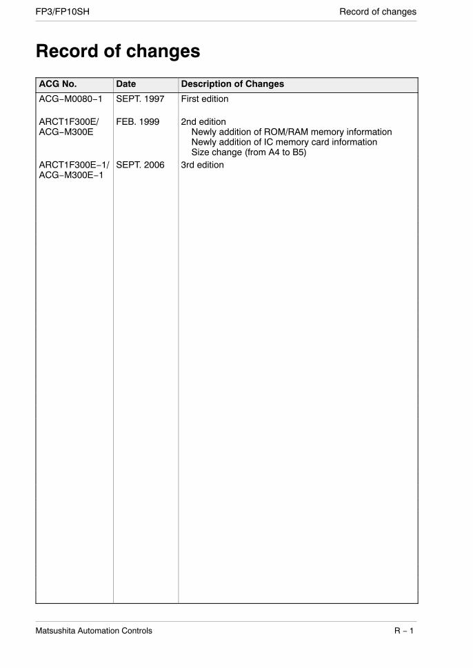
Record of changesFP3/FP10SH
R − 1Matsushita Automation Controls
Record of changes
ACG No. Date Description of Changes
ACG−M0080−1 SEPT. 1997 First edition
ARCT1F300E/ACG−M300E
FEB. 1999 2nd editionNewly addition of ROM/RAM memory informationNewly addition of IC memory card informationSize change (from A4 to B5)
ARCT1F300E−1/ACG−M300E−1
SEPT. 2006 3rd edition

Record of changes FP3/FP10SH
R − 2 Matsushita Automation Controls


ARCT1F300E-1 SEPT.06ACG-M300E-1