Embed Size (px)
Citation preview

EHS5-E/EHS5-US
Version: 00.000aDocId: EHS5_HID_v00.000a
Har
dwar
e In
terf
ace
Des
crip
tion

GENERAL NOTE THE USE OF THE PRODUCT INCLUDING THE SOFTWARE AND DOCUMENTATION (THE "PROD-UCT") IS SUBJECT TO THE RELEASE NOTE PROVIDED TOGETHER WITH PRODUCT. IN ANYEVENT THE PROVISIONS OF THE RELEASE NOTE SHALL PREVAIL. THIS DOCUMENT CONTAINSINFORMATION ON CINTERION PRODUCTS. THE SPECIFICATIONS IN THIS DOCUMENT ARE SUB-JECT TO CHANGE AT CINTERION'S DISCRETION. CINTERION WIRELESS MODULES GMBHGRANTS A NON-EXCLUSIVE RIGHT TO USE THE PRODUCT. THE RECIPIENT SHALL NOT TRANS-FER, COPY, MODIFY, TRANSLATE, REVERSE ENGINEER, CREATE DERIVATIVE WORKS; DISAS-SEMBLE OR DECOMPILE THE PRODUCT OR OTHERWISE USE THE PRODUCT EXCEPT ASSPECIFICALLY AUTHORIZED. THE PRODUCT AND THIS DOCUMENT ARE PROVIDED ON AN "ASIS" BASIS ONLY AND MAY CONTAIN DEFICIENCIES OR INADEQUACIES. TO THE MAXIMUMEXTENT PERMITTED BY APPLICABLE LAW, CINTERION WIRELESS MODULES GMBH DISCLAIMSALL WARRANTIES AND LIABILITIES. THE RECIPIENT UNDERTAKES FOR AN UNLIMITED PERIODOF TIME TO OBSERVE SECRECY REGARDING ANY INFORMATION AND DATA PROVIDED TO HIMIN THE CONTEXT OF THE DELIVERY OF THE PRODUCT. THIS GENERAL NOTE SHALL BE GOV-ERNED AND CONSTRUED ACCORDING TO GERMAN LAW.
CopyrightTransmittal, reproduction, dissemination and/or editing of this document as well as utilization of its con-tents and communication thereof to others without express authorization are prohibited. Offenders will beheld liable for payment of damages. All rights created by patent grant or registration of a utility model ordesign patent are reserved.
Copyright © 2012, Cinterion Wireless Modules GmbH
Trademark NoticeMicrosoft and Windows are either registered trademarks or trademarks of Microsoft Corporation in theUnited States and/or other countries. All other registered trademarks or trademarks mentioned in this doc-ument are property of their respective owners.
EHS5_HID_v00.000a Page 2 of 97 2012-06-08Confidential / Preliminary
EHS5-E/EHS5-US Hardware Interface Description
2
Document Name: EHS5-E/EHS5-US Hardware Interface Description
Version: 00.000a
Date: 2012-06-08
DocId: EHS5_HID_v00.000a
Status Confidential / Preliminary

EHS5-E/EHS5-US Hardware Interface Description Contents97
EHS5_HID_v00.000a Page 3 of 97 2012-06-08Confidential / Preliminary
Contents
1 Introduction ................................................................................................................. 81.1 Key Features at a Glance .................................................................................. 81.2 EHS5-E/EHS5-US System Overview .............................................................. 111.3 Circuit Concept ................................................................................................ 12
2 Interface Characteristics .......................................................................................... 132.1 Application Interface ........................................................................................ 13
2.1.1 Pad Assignment.................................................................................. 132.1.2 Signal Properties................................................................................. 15
2.1.2.1 Absolute Maximum Ratings ................................................ 192.1.3 USB Interface...................................................................................... 202.1.4 Serial Interface ASC0 ......................................................................... 212.1.5 Serial Interface ASC1 ......................................................................... 232.1.6 UICC/SIM/USIM Interface................................................................... 25
2.1.6.1 Enhanced ESD Protection for SIM Interface....................... 272.1.7 Digital Audio Interface......................................................................... 282.1.8 RTC Backup........................................................................................ 302.1.9 GPIO Interface .................................................................................... 312.1.10 I2C Interface ........................................................................................ 332.1.11 PWM Interfaces .................................................................................. 352.1.12 Control Signals.................................................................................... 35
2.1.12.1 Status LED .......................................................................... 352.1.12.2 Behavior of the RING0 Line (ASC0 Interface only) ............. 352.1.12.3 Power Indication Circuit ...................................................... 352.1.12.4 Host Wakeup....................................................................... 362.1.12.5 Fast Shutdown .................................................................... 37
2.2 RF Antenna Interface....................................................................................... 382.2.1 Antenna Interface Specifications ........................................................ 382.2.2 Antenna Installation ............................................................................ 422.2.3 RF Line Routing Design...................................................................... 43
2.2.3.1 Line Arrangement Examples............................................... 432.2.3.2 Routing Example................................................................. 48
2.3 Sample Application .......................................................................................... 49
3 Operating Characteristics ........................................................................................ 513.1 Operating Modes ............................................................................................. 513.2 Power Up/Power Down Scenarios................................................................... 52
3.2.1 Turn on EHS5-E/EHS5-US ................................................................. 523.2.1.1 Switch on EHS5-E/EHS5-US Using ON Signal .................. 523.2.1.2 Switch on EHS5-E/EHS5-US Using ON2 Signal ................ 54
3.2.2 Restart EHS5-E/EHS5-US.................................................................. 543.2.2.1 Restart EHS5-E/EHS5-US via AT+CFUN Command.......... 543.2.2.2 Restart EHS5-E/EHS5-US Using EMERG_RST................. 55
3.2.3 Signal States after Startup .................................................................. 56

EHS5-E/EHS5-US Hardware Interface Description Contents97
EHS5_HID_v00.000a Page 4 of 97 2012-06-08Confidential / Preliminary
3.2.4 Turn off EHS5-E/EHS5-US ................................................................. 573.2.4.1 Switch off EHS5-E/EHS5-US Using AT Command ............. 57
3.2.5 Automatic Shutdown ........................................................................... 583.2.5.1 Thermal Shutdown .............................................................. 583.2.5.2 Undervoltage Shutdown...................................................... 583.2.5.3 Overvoltage Shutdown........................................................ 58
3.3 Power Saving................................................................................................... 593.4 Power Supply................................................................................................... 60
3.4.1 Power Supply Ratings......................................................................... 603.4.2 Minimizing Power Losses ................................................................... 643.4.3 Measuring the Supply Voltage (VBATT+) ........................................... 64
3.5 Operating Temperatures.................................................................................. 653.6 Electrostatic Discharge .................................................................................... 66
3.6.1 Blocking against RF on Interface Lines .............................................. 663.7 Reliability Characteristics................................................................................. 69
4 Mechanical Dimensions, Mounting and Packaging............................................... 704.1 Mechanical Dimensions of EHS5-E/EHS5-US ................................................ 704.2 Mounting EHS5-E/EHS5-US onto the Application Platform............................. 72
4.2.1 SMT PCB Assembly ........................................................................... 724.2.1.1 Land Pattern and Stencil ..................................................... 724.2.1.2 Board Level Characterization.............................................. 74
4.2.2 Moisture Sensitivity Level ................................................................... 744.2.3 Soldering Conditions and Temperature .............................................. 75
4.2.3.1 Reflow Profile ...................................................................... 754.2.3.2 Maximum Temperature and Duration.................................. 76
4.2.4 Durability and Mechanical Handling.................................................... 774.2.4.1 Storage Conditions.............................................................. 774.2.4.2 Processing Life.................................................................... 784.2.4.3 Baking ................................................................................. 784.2.4.4 Electrostatic Discharge........................................................ 78
4.3 Packaging ........................................................................................................ 794.3.1 Tape and Reel .................................................................................... 79
4.3.1.1 Orientation........................................................................... 794.3.1.2 Barcode Label ..................................................................... 80
4.3.2 Shipping Materials .............................................................................. 814.3.2.1 Moisture Barrier Bag ........................................................... 814.3.2.2 Transportation Box .............................................................. 83
4.3.3 Trays ................................................................................................... 84
5 Regulatory and Type Approval Information ........................................................... 855.1 Directives and Standards................................................................................. 855.2 SAR requirements specific to portable mobiles ............................................... 885.3 Reference Equipment for Type Approval ......................................................... 895.4 Compliance with FCC and IC Rules and Regulations ..................................... 90

EHS5-E/EHS5-US Hardware Interface Description Contents97
EHS5_HID_v00.000a Page 5 of 97 2012-06-08Confidential / Preliminary
6 Document Information.............................................................................................. 916.1 Revision History ............................................................................................... 916.2 Related Documents ......................................................................................... 916.3 Terms and Abbreviations ................................................................................. 916.4 Safety Precaution Notes .................................................................................. 95
7 Appendix.................................................................................................................... 967.1 List of Parts and Accessories........................................................................... 96

EHS5-E/EHS5-US Hardware Interface Description Tables97
EHS5_HID_v00.000a Page 6 of 97 2012-06-08Confidential / Preliminary
Tables
Table 1: Pad assignments............................................................................................ 14Table 2: Signal properties ............................................................................................ 15Table 3: Absolute maximum ratings............................................................................. 19Table 4: Signals of the SIM interface (SMT application interface) ............................... 25Table 5: Overview of DAI pins...................................................................................... 28Table 6: GPIO assignment........................................................................................... 31Table 7: Host wakeup lines .......................................................................................... 36Table 8: Return loss in the active band........................................................................ 38Table 9: RF Antenna interface GSM / UMTS............................................................... 38Table 10: Overview of operating modes ........................................................................ 51Table 11: Signal states................................................................................................... 56Table 12: Power supply ratings (TBD.) .......................................................................... 60Table 13: Board temperature ......................................................................................... 65Table 14: Electrostatic values ........................................................................................ 66Table 15: EMI measures on the application interface.................................................... 68Table 16: Summary of reliability test conditions............................................................. 69Table 17: Reflow temperature ratings ............................................................................ 75Table 18: Storage conditions ......................................................................................... 77Table 19: Directives ....................................................................................................... 85Table 20: Standards of North American type approval .................................................. 85Table 21: Standards of European type approval............................................................ 85Table 22: Requirements of quality ................................................................................. 86Table 23: Standards of the Ministry of Information Industry of the
People’s Republic of China............................................................................ 86Table 24: Toxic or hazardous substances or elements with defined concentration
limits ............................................................................................................... 87Table 25: List of parts and accessories.......................................................................... 96Table 26: Molex sales contacts (subject to change) ...................................................... 97

EHS5-E/EHS5-US Hardware Interface Description Figures97
EHS5_HID_v00.000a Page 7 of 97 2012-06-08Confidential / Preliminary
Figures
Figure 1: EHS5-E/EHS5-US system overview.............................................................. 11Figure 2: EHS5-E/EHS5-US block diagram (TBD.)....................................................... 12Figure 3: Numbering plan for connecting pads (bottom view)....................................... 13Figure 4: USB circuit ..................................................................................................... 20Figure 5: Serial interface ASC0..................................................................................... 21Figure 6: ASC0 startup behavior ................................................................................... 22Figure 7: Serial interface ASC1..................................................................................... 23Figure 8: ASC1 startup behavior ................................................................................... 24Figure 9: External UICC/SIM/USIM card holder circuit ................................................. 26Figure 10: SIM interface - enhanced ESD protection...................................................... 27Figure 11: Long frame PCM timing, 256kHz ................................................................... 28Figure 12: DAI startup timing........................................................................................... 29Figure 13: RTC supply variants....................................................................................... 30Figure 14: GPIO startup behavior ................................................................................... 32Figure 15: I2C interface connected to V180 .................................................................... 33Figure 16: I2C startup behavior ....................................................................................... 34Figure 17: Status signalling with LED driver.................................................................... 35Figure 18: Power indication circuit .................................................................................. 36Figure 19: Antenna pads (bottom view) .......................................................................... 42Figure 20: Embedded Stripline with 65µm prepreg (1080) and 710µm core .................. 43Figure 21: Micro-Stripline on 1.0mm standard FR4 2-layer PCB - example 1 ................ 44Figure 22: Micro-Stripline on 1.0mm Standard FR4 PCB - example 2............................ 45Figure 23: Micro-Stripline on 1.5mm Standard FR4 PCB - example 1............................ 46Figure 24: Micro-Stripline on 1.5mm Standard FR4 PCB - example 2............................ 47Figure 25: Routing to application‘s RF connector - top view........................................... 48Figure 26: Schematic diagram of EHS5-E/EHS5-US sample application ....................... 50Figure 27: ON circuit sample........................................................................................... 52Figure 28: ON timing ....................................................................................................... 53Figure 29: ON2 timing ..................................................................................................... 54Figure 30: Emergency restart timing ............................................................................... 55Figure 31: Switch off behavior......................................................................................... 57Figure 32: Power supply limits during transmit burst....................................................... 64Figure 33: Position of reference points BATT+and GND ................................................ 64Figure 34: EMI circuits..................................................................................................... 67Figure 35: EHS5-E/EHS5-US– top and bottom view ...................................................... 70Figure 36: Dimensions of EHS5-E/EHS5-US (all dimensions in mm)............................. 71Figure 37: Land pattern (top view) .................................................................................. 72Figure 38: Recommended design for 110 micron thick stencil (top view) ....................... 73Figure 39: Recommended design for 150 micron thick stencil (top view) ....................... 73Figure 40: Reflow Profile ................................................................................................. 75Figure 41: Carrier tape .................................................................................................... 79Figure 42: Reel direction ................................................................................................. 79Figure 43: Barcode label on tape reel ............................................................................. 80Figure 44: Moisture barrier bag (MBB) with imprint......................................................... 81Figure 45: Moisture Sensitivity Label .............................................................................. 82Figure 46: Humidity Indicator Card - HIC ........................................................................ 83Figure 47: Small quantity tray.......................................................................................... 84Figure 48: Tray to ship odd module amounts.................................................................. 84Figure 49: Trays with packaging materials...................................................................... 84Figure 50: Reference equipment for Type Approval ....................................................... 89

EHS5-E/EHS5-US Hardware Interface Description1 Introduction12
EHS5_HID_v00.000a Page 8 of 97 2012-06-08Confidential / Preliminary
1 Introduction
This document1 describes the hardware of the Cinterion EHS5-E/EHS5-US module. It helps you quickly retrieve interface specifications, electrical and mechanical details and information on the requirements to be considered for integrating further components.
1.1 Key Features at a Glance
1. The document is effective only if listed in the appropriate Release Notes as part of the technicaldocumentation delivered with your Cinterion product.
Feature Implementation
General
Frequency bands EHS5-E: GSM/GPRS/EDGE: Dual band GSM 900/1800MHzUMTS/HSPA+: Dual band UMTS 900/2100MHz
EHS5-US: GSM/GPRS/EDGE: Dual band GSM 850/1900MHzUMTS/HSPA+: Dual band UMTS 850/1900MHz
GSM class Small MS
Output power (according to Release 99, V5)
EHS5-E:Class 4 (+33dBm ±2dB) for EGSM900Class 1 (+30dBm ±2dB) for GSM1800Class E2 (+27dBm ± 3dB) for GSM 900 8-PSKClass E2 (+26dBm +3 /-4dB) for GSM 1800 8-PSKClass 3 (+24dBm +1/-3dB) for UMTS 2100, WCDMA FDD BdIClass 3 (+24dBm +1/-3dB) for UMTS 900, WCDMA FDD BdVIII
EHS5-US: Class 4 (+33dBm ±2dB) for EGSM850Class 1 (+30dBm ±2dB) for GSM1900Class E2 (+27dBm ± 3dB) for GSM 850 8-PSKClass E2 (+26dBm +3 /-4dB) for GSM 1900 8-PSKClass 3 (+24dBm +1/-3dB) for UMTS 1900,WCDMA FDD BdIIClass 3 (+24dBm +1/-3dB) for UMTS 850, WCDMA FDD BdV
Power supply 3.3V to 4.5V
Operating temperature (board temperature)
Normal operation: TBD.Extended operation: TBD.
Physical Dimensions: 27.6mm x 18.8mm x 2.3mmWeight: approx. 3g
RoHS All hardware components fully compliant with EU RoHS Directive

EHS5-E/EHS5-US Hardware Interface Description1.1 Key Features at a Glance12
EHS5_HID_v00.000a Page 9 of 97 2012-06-08Confidential / Preliminary
HSPA features
3GPP Release 6, 7 DL 7.2Mbps, UL 5.7MbpsHSDPA Cat.8 / HSUPA Cat.6 data ratesCompressed mode (CM) supported according to 3GPP TS25.212
UMTS features
3GPP Release 4 PS data rate – 384 kbps DL / 384 kbps ULCS data rate – 64 kbps DL / 64 kbps UL
GSM/GPRS/EGPRS features
Data transfer GPRS:• Multislot Class 12• Full PBCCH support• Mobile Station Class B• Coding Scheme 1 – 4EGPRS:• Multislot Class 12• EDGE E2 power class for 8 PSK• Downlink coding schemes – CS 1-4, MCS 1-9• Uplink coding schemes – CS 1-4, MCS 1-9• SRB loopback and test mode B• 8-bit, 11-bit RACH• PBCCH support• 1 phase/2 phase access procedures• Link adaptation and IR• NACC, extended UL TBF• Mobile Station Class BCSD:• V.110, RLP, non-transparent• 14.4kbps• USSD
SMS Point-to-point MT and MOCell broadcastText and PDU modeStorage: SIM card plus SMS locations in mobile equipment
Software
AT commands Hayes 3GPP TS 27.007, TS 27.005, CinterionAT commands for RIL compatibility (available as of Release 2)
Microsoft™ compatibility RIL for Pocket PC and Smartphone (available as of Release 2)
SIM Application Toolkit SAT Release 99 (available as of Release 2)
Firmware update Generic update from host application over ASC0 or ASC1.
Feature Implementation

EHS5-E/EHS5-US Hardware Interface Description1.1 Key Features at a Glance12
EHS5_HID_v00.000a Page 10 of 97 2012-06-08Confidential / Preliminary
Interfaces
Module interface Surface mount device with solderable connection pads (SMT application interface). Land grid array (LGA) technology ensures high solder joint reli-ability and provides the possibility to use an optional module mounting socket.
For more information on how to integrate SMT modules see also [3]. This application note comprises chapters on module mounting and application layout issues as well as on additional SMT application development equip-ment.
USB USB 2.0 High Speed (480Mbit/s) device interface, Full Speed (12Mbit/s)compliant
2 serial interfaces ASC0:• 8-wire modem interface with status and control lines, unbalanced, asyn-
chronous• Adjustable baud rates: 1,200bps to 921,600bps• Autobauding: 1,200bps to 921,600bps• Supports RTS0/CTS0 hardware flow control.• Multiplex ability according to GSM 07.10 Multiplexer Protocol.ASC1:• 4-wire, unbalanced asynchronous interface• Adjustable baud rates: 1,200bps to 921,60bps• Supports RTS1/CTS1 hardware flow control
Audio 1 digital interface (PCM)
UICC interface Supported SIM/USIM cards: 3V, 1.8V
GPIO interface GPIO interface with 4 GPIO lines. The GPIO interface is shared with LED signalling and PWM functionality (available as of Release 2).
I2C interface Supports I2C serial interface (available as of Release 2)
Antenna interface pads 50
Power on/off, Reset
Power on/off Switch-on by hardware signal ONSwitch-off by AT command Switch off by hardware signal FAST_SHTDWN instead of AT commandAutomatic switch-off in case of critical temperature and voltage conditions.
Reset Orderly shutdown and reset by AT commandEmergency reset by hardware signal EMERG_RST
Special features
Real time clock Timer functions via AT commands
Phonebook SIM and phone
TTY/CTM support Integrated CTM modem
Evaluation kit
Evaluation module EHS5-E/EHS5-US module soldered onto a dedicated PCB that can be con-nected to an adapter in order to be mounted onto the DSB75.
DSB75 DSB75 Development Support Board designed to test and type approve Cinterion Wireless Modules and provide a sample configuration for applica-tion engineering. A special adapter is required to connect the EHS5-E/EHS5-US evaluation module to the DSB75.
Feature Implementation
EHS5-E/EHS5-US Hardware Interface Description1.2 EHS5-E/EHS5-US System Overview12
EHS5_HID_v00.000a Page 11 of 97 2012-06-08Confidential / Preliminary
1.2 EHS5-E/EHS5-US System Overview
Figure 1: EHS5-E/EHS5-US system overview
GPIO interface
I2C
USB
ASC0
ASC1
CONTROL
RTC
POWER
ANTENNA (GSM/UMTS dual band)
Module
SIM interface(with SIM detection)
SIM card
Application
Power supply
Backup supply
Emergency reset
ON, ON2
Serial interface
Serial modem interface
I2C
GPIO
38
45
21
21
12
USB
Antenna
1
PCMDigital audio(PCM)
4
Status LED / GPIO1
DAC (PWM) PWM / GPIO2
Fast shutdown Fast shutdown11
ADC ADC1

EHS5-E/EHS5-US Hardware Interface Description1.3 Circuit Concept12
EHS5_HID_v00.000a Page 12 of 97 2012-06-08Confidential / Preliminary
1.3 Circuit Concept
Figure 2 shows a block diagram of the EHS5-E/EHS5-US module and illustrates the major functional components:
Baseband block:• GSM baseband processor and power management• Stacked flash/PSRAM memory• Application interface (SMT with connecting pads)GSM RF section:• RF transceiver (part of baseband processor IC)• RF power amplifier/front-end module inc. harmonics filtering• Receive SAW filters
Figure 2: EHS5-E/EHS5-US block diagram (TBD.)
TBD.

EHS5-E/EHS5-US Hardware Interface Description2 Interface Characteristics50
EHS5_HID_v00.000a Page 13 of 97 2012-06-08Confidential / Preliminary
2 Interface Characteristics
EHS5-E/EHS5-US is equipped with an SMT application interface that connects to the external application. The SMT application interface incorporates the various application interfaces as well as the RF antenna interface.
2.1 Application Interface
2.1.1 Pad Assignment
The SMT application interface on the EHS5-E/EHS5-US provides connecting pads to integratethe module into external applications. Figure 3 shows the connecting pads’ numbering plan,the following Table 1 lists the pads’ assignments.
Figure 3: Numbering plan for connecting pads (bottom view)
53
65
64
63
62
61
60
59
58
57
56
55
54
66
33
21
22
23
24
25
26
27
28
29
30
31
32
20
106
9291
9897969594
9089
85 86
93
74
99
87 88
8483
7978777675
8281
80
727170696867
105104103102101100
73
44
19181716151413121110987654321
343536373839404142434546474849505152
Supply pads: BATT+
Control pads
GND pads
ASC0 pads
ASC1 pads
SIM pads RF antenna pad
I2C pads
ADC pad
Supply pads: Other
Digital audio pads (PCM)
Combined GPIO/Control pads(LED, PWM)
Do not use
USB pads
GPIO pad

EHS5-E/EHS5-US Hardware Interface Description2.1 Application Interface50
EHS5_HID_v00.000a Page 14 of 97 2012-06-08Confidential / Preliminary
Signal pads that are not used should not be connected to an external application.
Please note that the reference voltages listed in Table 2 are the values measured directly onthe EHS5-E/EHS5-US module. They do not apply to the accessories connected.
Table 1: Pad assignments
Pad no. Signal name Pad no. Signal name Pad no. Signal name
1 Do not use 23 TXDDAI 45 USB_DP
2 Do not use 24 TFSDAI 46 USB_DN
3 Do not use 25 RXDDAI 47 GND
4 GND 26 SCLK 48 GND
5 BATT+ 27 I2CDAT 49 GND
6 GND 28 I2CCLK 50 GND
7 ADC1 29 TXD1 51 GND
8 ON 30 RXD1 52 GND
9 GND 31 RTS1 53 BATT+
10 V180 32 CTS1 54 GND
11 RXD0 33 EMERG_RST 55 GND
12 CTS0 34 GND 56 GND
13 TXD0 35 Do not use 57 GND
14 RING0 36 GPIO8 58 GND
15 RTS0 37 GPIO7/PWM1 59 RF_OUT
16 VDDLP 38 GPIO6/PWM2 60 GND
17 CCRST 39 GPIO5/LED 61 GND
18 CCIN 40 FAST_SHTDWN 62 GND
19 CCIO 41 DSR0 63 GND
20 CCVCC 42 DCD0 64 Do not use
21 CCCLK 43 DTR0 65 Do not use
22 VCORE 44 VUSB 66 Do not use
Centrally located pads
67 Do not use 81 GND 95 GND
68 Do not use 82 GND 96 GND
69 Do not use 83 GND 97 GND
70 Do not use 84 GND 98 Do not use
71 Do not use 85 GND 99 GND
72 Do not use 86 GND 100 GND
73 Do not use 87 Do not use 101 GND
74 Do not use 88 GND 102 GND
75 Do not use 89 GND 103 GND
76 Do not use 90 GND 104 GND
77 Do not use 91 Do not use 105 GND
78 Do not use 92 GND 106 GND
79 ON2 93 GND
80 Do not use 94 GND

EHS5-E/EHS5-US Hardware Interface Description2.1 Application Interface50
EHS5_HID_v00.000a Page 15 of 97 2012-06-08Confidential / Preliminary
2.1.2 Signal Properties
Table 2: Signal properties
Function Signal name IO Signal form and level Comment
Power supply
BATT+GSM activated
I VImax = 4.5VVInorm = 3.8VVImin = 3.3V during Tx burst on board
I TBD.A, during Tx burst (GSM)
Lines of BATT+ and GND must be connected in parallel for supply pur-poses because higher peak currents may occur.
Minimum voltage must not fall below 3.3V includ-ing drop, ripple, spikes.
BATT+ assigned to pad 5 requires an additional ESR 150µF capacitor.
n Tx = n x 577µs peak current every 4.616ms
BATT+WCDMA activated
I VImax = 4.5VVInorm = 3.8VVImin = 3.3V during Transmit active.Imax=800mA during Tx
BATT+ I VImax = 4.5VVInorm = 3.8VVImin = 3.3V Imax = 250mA during Tx
Power supply
GND Ground Application Ground
External supply voltage
V180 O Normal operation:VOnorm = 1.80V ±3%IOmax = -10mA
SLEEP mode Operation:VOSleep = 1.80V ±5%IOmax = -10mA
CLmax = 100nF
V180 may be used to supply level shifters at the interfaces or to supply external application cir-cuits.
VCORE and V180 should be used for the power indication circuit.
If unused keep line open.VCORE O VOnorm = 1.2VIOmax = -10mA
CLmax = 100nF
Ignition ON I VIHmax = VDDLP + 0.3VVIHmin = 1.2VVILmax = 0.5VRise Time min = 50µs, max = 80µsMin low time before rising edge <=100µs
ON ___↑____ high impulse
This signal switches the module ON.
This line is high level edge triggered.
ON2 I VOHmax = VDDLP maxVIHmin = 1.2VVILmax = 0.5VLow level time >= 50µs
ON2 ~~~~|___ low level signal
This signal switches the module ON.
This line is low level sen-sitive triggered.

EHS5-E/EHS5-US Hardware Interface Description2.1 Application Interface50
EHS5_HID_v00.000a Page 16 of 97 2012-06-08Confidential / Preliminary
Emergency restart
EMERG_RST I RI 1k, CI 1nFVOHmax = VDDLP maxVIHmin = 1.35VVILmax = 0.3V at ~200µA
~~|___|~~ low impulse width > 10ms
This line must be driven low by an open drain or open collector driver con-nected to GND.
If unused keep line open.
Fast shutdown
FAST_SHTDWN
I VILmax = 0.35VVIHmin = 1.30V VIHmax = 1.85V
~~|___|~~ low impulse width > 10ms
This line must be driven low.If unused keep line open.
RTC backup
VDDLP I/O VOnorm = 1.8V IOmax = 5mA
VImax = 1.9VVImin = 1.0VIItyp = TBD.
It is recommended to use a serial resistor between VDDLP and a possible capacitor.
If unused keep line open.
USB VUSB_IN I VImin = 3VVImax = 5.25V
Active current: Ityp = TBD.µA (max TBD.µA)
Suspend current: Ityp = TBD.µA (max TBD.µA)
All electrical characteris-tics according to USB Implementers' Forum, USB 2.0 Specification.
If unused keep line open.
USB_DN I/O Full and high speed signal characteris-tics according USB 2.0 Specification.
USB_DP
Serial Interface ASC0
RXD0 O VOLmax = 0.25V at I = 1mAVOHmin = 1.55V at I = -1mAVOHmax = 1.85V
VILmax = 0.35VVIHmin = 1.30V VIHmax = 1.85V
If unused keep line open.
TXD0 I
RTS0 I
CTS0 O
DTR0 I
DSR0 O
DCD0 O
RING0 O
Serial Interface ASC1
RXD1 O VOLmax = 0.25V at I = 1mAVOHmin = 1.55V at I = -1mAVOHmax = 1.65V
VILmax = 0.35VVIHmin = 1.30V VIHmax = 1.85V
If unused keep line open.
TXD1 I
RTS1 I
CTS1 O
Table 2: Signal properties
Function Signal name IO Signal form and level Comment

EHS5-E/EHS5-US Hardware Interface Description2.1 Application Interface50
EHS5_HID_v00.000a Page 17 of 97 2012-06-08Confidential / Preliminary
SIM card detection
CCIN I RI 110kVIHmin = 1.45V at I = 15µA, VIHmax= 1.9VVILmax = 0.3V
CCIN = High, SIM card inserted.
For details please refer to Section 2.1.6.
If unused keep line open.
3V SIM Card Inter-face
CCRST O VOLmax = 0.30V at I = 1mAVOHmin = 2.45V at I = -1mAVOHmax = 2.90V
Maximum cable length or copper track to SIM card holder should not exceed 100mm.
CCIO I/O VILmax = 0.50VVIHmin = 2.05VVIHmax = 2.90V
VOLmax = 0.25V at I = 1mAVOHmin = 2.50V at I = -1mAVOHmax = 2.90V
CCCLK O VOLmax = 0.25V at I = 1mAVOHmin = 2.40V at I = -1mAVOHmax = 2.90V
CCVCC O VOmin = 2.80V VOtyp = 2.85VVOmax = 2.90VIOmax = -30mA
1.8V SIM Card Inter-face
CCRST O VOLmax = 0.25V at I = 1mAVOHmin = 1.45V at I = -1mAVOHmax = 1.90V
CCIO I/O VILmax = 0.35VVIHmin = 1.25VVIHmax = 1.85V
VOLmax = 0.25V at I = 1mAVOHmin = 1.50V at I = -1mAVOHmax = 1.85V
CCCLK O VOLmax = 0.25V at I = 1mAVOHmin = 1.50V at I = -1mAVOHmax = 1.85V
CCVCC O VOmin = 1.75V VOtyp = 1.80VVOmax = 1.85VIOmax = -30mA
Table 2: Signal properties
Function Signal name IO Signal form and level Comment

EHS5-E/EHS5-US Hardware Interface Description2.1 Application Interface50
EHS5_HID_v00.000a Page 18 of 97 2012-06-08Confidential / Preliminary
I2C I2CCLK IO Open drain IOVOLmin = 0.35V at I = -3mAVOHmax = 1.85VR external pull up min = 560Ohm
VILmax = 0.35VVIHmin = 1.3VVIHmax = 1.85V
According to the I2C Bus Specification Version 2.1 for the fast mode a rise time of max. 300ns is per-mitted. There is also a maximum VOL=0.4V at 3mA specified.
The value of the pull-up depends on the capaci-tive load of the whole sys-tem (I2C Slave + lines). The maximum sink cur-rent of I2CDAT and I2CCLK is 4mA.
If lines are unused keep lines open.
I2CDAT IO
GPIO interface
GPIO5 IO VOLmax = 0.25V at I = 1mAVOHmin = 1.55V at I = -1mAVOHmax = 1.85V
VILmax = 0.335VVIHmin = 1.30V VIHmax = 1.85V
If unused keep line open.
Please note that some GPIO lines can be used for functions other than GPIO: Status LED line: GPIO5PWM: GPIO6/GPIO7
GPIO6 IO
GPIO7 IO
GPIO8 IO
Digital audio inter-face (PCM)
TFSDAI O VOLmax = 0.25V at I = 1mAVOHmin = 1.55V at I = -1mAVOHmax = 1.85V
If unused keep line open.
SCLK O
TXDDAI O
RXDDAI I VILmax = 0.35VVIHmin = 1.30VVIHmax = 1.85V
ADC ADC1 I RI = 1MVI = 0V ... 1.2V (valid range)VIH max = 1.2V
If unused keep line open.
The ADC functionality will be available as of Release 2.
Table 2: Signal properties
Function Signal name IO Signal form and level Comment

EHS5-E/EHS5-US Hardware Interface Description2.1 Application Interface50
EHS5_HID_v00.000a Page 19 of 97 2012-06-08Confidential / Preliminary
2.1.2.1 Absolute Maximum Ratings
The absolute maximum ratings stated in Table 3 are stress ratings under any conditions. Stresses beyond any of these limits will cause permanent damage to EHS5-E/EHS5-US.
Table 3: Absolute maximum ratings
Parameter Min Max Unit
Supply voltage BATT+ -0.5 +5.5 V
Voltage at all digital lines in POWER DOWN mode -0.3 +0.3 V
Voltage at digital lines in normal operation -0.3 +2.1 V
Voltage at SIM/USIM interface -0.5 +3.3 V
VDDLP input voltage -0.15 2.0 V
VUSB_IN, USB_DN, USB_DP TBD. TBD. V
Voltage at analog lines in POWER DOWN mode -0.3 +0.3 mA

EHS5-E/EHS5-US Hardware Interface Description2.1 Application Interface50
EHS5_HID_v00.000a Page 20 of 97 2012-06-08Confidential / Preliminary
2.1.3 USB Interface
EHS5-E/EHS5-US supports a USB 2.0 High Speed (480Mbit/s) device interface that is Full Speed (12Mbit/s) compliant. The USB interface is primarily intended for use as command and data interface and for downloading firmware.
The USB host is responsible for supplying the VUSB_IN line. This line is for voltage detection only. The USB part (driver and transceiver) is supplied by means of BATT+. This is because EHS5-E/EHS5-US is designed as a self-powered device compliant with the “Universal Serial Bus Specification Revision 2.0”1.
Figure 4: USB circuit
To properly connect the module's USB interface to the host a USB 2.0 compatible connector is required. For more information on the USB related signals see Table 2. Furthermore, the USB modem driver distributed with EHS5-E/EHS5-US needs to be installed.
While the USB connection is active, the module will not change into SLEEP Mode. To enable switching into SLEEP mode the USB host must bring its USB interface into Suspend state. Al-so, VUSB_IN should always be kept enabled for this functionality. See “Universal Serial Bus Specification Revision 2.0“1 for a description of the Suspend state. On incoming calls EHS5-E/EHS5-US will then generate a remote wake up request to resume the USB connection (active low).
As an alternative to the regular USB remote wakeup mechanism it is possible to employ the RING0 line to wake up the host application. The benefit is that the RING0 line can wake up the host application in case of incoming calls or other events signalized by URCs while the USB interface is suspended or shut down. For details on this host wakeup interface see Section 2.1.12.4.
1. The specification is ready for download on http://www.usb.org/developers/docs/
VBUS
DPDN
VREG (3V075)BATT+
USB_DP2)
lin. reg.GND
Module
Detection onlyVUSB_IN
USB part1)
RING0Host wakeup
1) All serial (including RS) and pull-up resistors for data lines are implemented.
USB_DN2)
2) If the USB interface is operated in High Speed mode (480MHz), it is recommended to take special care routing the data lines USB_DP and USB_DN. Application layout should in this case implement a differential impedance of 90Ohm for proper signal integrity.
RS
RS
SMT

EHS5-E/EHS5-US Hardware Interface Description2.1 Application Interface50
EHS5_HID_v00.000a Page 21 of 97 2012-06-08Confidential / Preliminary
2.1.4 Serial Interface ASC0
EHS5-E/EHS5-US offers an 8-wire unbalanced, asynchronous modem interface ASC0 con-forming to ITU-T V.24 protocol DCE signalling. The electrical characteristics do not comply with ITU-T V.28. The significant levels are 0V (for low data bit or active state) and 1.8V (for high data bit or inactive state). For electrical characteristics please refer to Table 2. For an illustration of the interface line’s startup behavior see Figure 6.
EHS5-E/EHS5-US is designed for use as a DCE. Based on the conventions for DCE-DTE con-nections it communicates with the customer application (DTE) using the following signals:• Port TXD @ application sends data to the module’s TXD0 signal line• Port RXD @ application receives data from the module’s RXD0 signal line
Figure 5: Serial interface ASC0
Features:• Includes the data lines TXD0 and RXD0, the status lines RTS0 and CTS0 and, in addition,
the modem control lines DTR0, DSR0, DCD0 and RING0.• ASC0 is designed for controlling GSM/UMTS voice calls, transferring data and for control-
ling the module with AT commands.• Full multiplexing capability allows the interface to be partitioned into virtual channels.• The RING0 signal serves to indicate incoming calls and other types of URCs (Unsolicited
Result Code). It can also be used to send pulses to the host application, for example towake up the application from power saving state.
• Configured for 8 data bits, no parity and 1 stop bit. • ASC0 can be operated at fixed bit rates from 1200bps up to 921600bps.• Autobauding supports bit rates from 1200bps up to 921600bps.• Supports RTS0/CTS0 hardware flow control.• Wake up from SLEEP mode by RTS0 activation (high to low transition).

EHS5-E/EHS5-US Hardware Interface Description2.1 Application Interface50
EHS5_HID_v00.000a Page 22 of 97 2012-06-08Confidential / Preliminary
The following figure shows the startup behavior of the asynchronous serial interface ASC0.
*) For pull-up and pull-down values see Table 11.
Figure 6: ASC0 startup behavior
Please note that no data must be sent over the ASC0 interface before the interface is activeand ready to receive data (see Section 3.2.1.1).
TXD0
RXD0
RTS0
CTS0
DTR0
DSR0
DCD0
RING0
ON / ON2
EMERG_RST
PU
PD
PD
PD
PD
PU
PD
PU
Power supply activeStart up
Firmware initialization
Command interface initialization
Interface active
Resetstate
V180
VCORE
PD

EHS5-E/EHS5-US Hardware Interface Description2.1 Application Interface50
EHS5_HID_v00.000a Page 23 of 97 2012-06-08Confidential / Preliminary
2.1.5 Serial Interface ASC1
EHS5-E/EHS5-US offers a 4-wire unbalanced, asynchronous modem interface ASC1 conform-ing to ITU-T V.24 protocol DCE signalling. The electrical characteristics do not comply with ITU-T V.28. The significant levels are 0V (for low data bit or active state) and 1.8V (for high data bitor inactive state). For electrical characteristics please refer to Table 2. For an illustration of theinterface line’s startup behavior see Figure 8.
EHS5-E/EHS5-US is designed for use as a DCE. Based on the conventions for DCE-DTE con-nections it communicates with the customer application (DTE) using the following signals:• Port TXD @ application sends data to module’s TXD1 signal line• Port RXD @ application receives data from the module’s RXD1 signal line
Figure 7: Serial interface ASC1
Features• Includes only the data lines TXD1 and RXD1 plus RTS1 and CTS1 for hardware hand-
shake. • On ASC1 no RING line is available.• Configured for 8 data bits, no parity and 1 or 2 stop bits.• ASC1 can be operated at fixed bit rates from 1,200 bps to 921600 bps. Autobauding is not
supported on ASC1. • Supports RTS1/CTS1 hardware flow.

EHS5-E/EHS5-US Hardware Interface Description2.1 Application Interface50
EHS5_HID_v00.000a Page 24 of 97 2012-06-08Confidential / Preliminary
The following figure shows the startup behavior of the asynchronous serial interface ASC1.
*) For pull-down values see Table 11.
Figure 8: ASC1 startup behavior
TXD1
RXD1
RTS1
CTS1
ON / ON2
EMERG_RST
PD
PD
PD
PD
Power supply activeStart up
Firmware initialization
Command interface initialization
Interface active
Resetstate
V180
VCORE
PD

EHS5-E/EHS5-US Hardware Interface Description2.1 Application Interface50
EHS5_HID_v00.000a Page 25 of 97 2012-06-08Confidential / Preliminary
2.1.6 UICC/SIM/USIM Interface
EHS5-E/EHS5-US has an integrated UICC/SIM/USIM interface compatible with the 3GPP 31.102 and ETSI 102 221. This is wired to the host interface in order to be connected to an external SIM card holder. Five pads on the SMT application interface are reserved for the SIM interface.
The UICC/SIM/USIM interface supports 3V and 1.8V SIM cards. Please refer to Table 2 for electrical specifications of the UICC/SIM/USIM interface lines depending on whether a 3V or 1.8V SIM card is used.
The CCIN signal serves to detect whether a tray (with SIM card) is present in the card holder. Using the CCIN signal is mandatory for compliance with the GSM 11.11 recommendation if the mechanical design of the host application allows the user to remove the SIM card during oper-ation. To take advantage of this feature, an appropriate SIM card detect switch is required on the card holder. For example, this is true for the model supplied by Molex, which has been test-ed to operate with EHS5-E/EHS5-US and is part of the Cinterion reference equipment submit-ted for type approval. See Section 7.1 for Molex ordering numbers.
Note: No guarantee can be given, nor any liability accepted, if loss of data is encountered after removing the SIM card during operation. Also, no guarantee can be given for properly initializ-ing any SIM card that the user inserts after having removed the SIM card during operation. In this case, the application must restart EHS5-E/EHS5-US.
Table 4: Signals of the SIM interface (SMT application interface)
Signal Description
GND Separate ground connection for SIM card to improve EMC.
CCCLK Chipcard clock
CCVCC SIM supply voltage.
CCIO Serial data line, input and output.
CCRST Chipcard reset
CCIN Input on the baseband processor for detecting a SIM card tray in the holder. If the SIM is removed during operation the SIM interface is shut down immediately to prevent destruc-tion of the SIM. The CCIN signal is active low.The CCIN signal is mandatory for applications that allow the user to remove the SIM card during operation. The CCIN signal is solely intended for use with a SIM card. It must not be used for any other purposes. Failure to comply with this requirement may invalidate the type approval of EHS5-E/EHS5-US.

EHS5-E/EHS5-US Hardware Interface Description2.1 Application Interface50
EHS5_HID_v00.000a Page 26 of 97 2012-06-08Confidential / Preliminary
The figure below shows a circuit to connect an external SIM card holder.
Figure 9: External UICC/SIM/USIM card holder circuit
The total cable length between the SMT application interface pads on EHS5-E/EHS5-US and the pads of the external SIM card holder must not exceed 100mm in order to meet the specifi-cations of 3GPP TS 51.010-1 and to satisfy the requirements of EMC compliance.
To avoid possible cross-talk from the CCCLK signal to the CCIO signal be careful that both lines are not placed closely next to each other. A useful approach is using a GND line to shield the CCIO line from the CCCLK line.
An example for an optimized ESD protection for the SIM interface is shown in Section 2.1.6.1.
SIM
CCVCC
CCRST
CCIO
CCCLK
220nF
1nF
CCIN
V180

EHS5-E/EHS5-US Hardware Interface Description2.1 Application Interface50
EHS5_HID_v00.000a Page 27 of 97 2012-06-08Confidential / Preliminary
2.1.6.1 Enhanced ESD Protection for SIM Interface
To optimize ESD protection for the SIM interface it is possible to add ESD diodes to the SIM interface lines as shown in the example given in Figure 10.
The example was designed to meet ESD protection according ETSI EN 301 489-1/7: Contact discharge: ± 4kV, air discharge: ± 8kV.
Figure 10: SIM interface - enhanced ESD protection
CCRST
CCCLK
CCIO
CCVCC
CCINGND
1 2 3
6 5 4
SIM_RST
SIM_CLK
SIM_IO
SIM_VCC
SIM_DET
Module

EHS5-E/EHS5-US Hardware Interface Description2.1 Application Interface50
EHS5_HID_v00.000a Page 28 of 97 2012-06-08Confidential / Preliminary
2.1.7 Digital Audio Interface
EHS5-E/EHS5-US’s digital audio interface (DAI) can be used to connect audio devices capableof pulse code modulation (PCM). The PCM functionality allows for the use of an external codeclike the MC145483.
The DAI interface supports a 256kHz, long frame synchronization master mode with the follow-ing features:• 16 Bit linear• 8kHz sample rate• The most significant bit MSB is transferred first• 125µs frame duration• Common frame sync signal for transmit and receive
Table 5 describes the available DAI pins at the digital audio interface. For electrical details seeSection 2.1.2.
Figure 11 shows the PCM timing for the master mode available with EHS5-E/EHS5-US.
Figure 11: Long frame PCM timing, 256kHz
Table 5: Overview of DAI pins
Signal name onB2B connector
Pin direction Input/Output
TXDDAI O PCM data from EHS5-E/EHS5-US to external codec.
RXDDAI I PCM data from external codec to EHS5-E/EHS5-US.
TFSDAI O Frame synchronization signal to external codec:Long frame @ 256kHz
SCLK O Bit clock to external codec: 256kHz
SCLK
TXDDAI
RXDDAI
TFSDAI
MSB
MSB
LSB
LSB
14 13
14 13
1
1
12
12
2
2
MSB
MSB
125 µs

EHS5-E/EHS5-US Hardware Interface Description2.1 Application Interface50
EHS5_HID_v00.000a Page 29 of 97 2012-06-08Confidential / Preliminary
The following figure shows the start up behaviour of the DAI interface. The start up configura-tion of functions will be activated after the software initialization of the command interface. Withan active state of RING0, CTS0 or CTS1 (low level) the initialization of the DAI interface is fin-ished.
Figure 12: DAI startup timing
RXDDAI
TFSDAI
SCLK
TXDDAI
PD
PD
PD
PD
CTS0
ON / ON2
EMERG_RST
Power supply activeStart up
Firmware initialization
Command interface initialization
Interface active
Resetstate
V180
VCORE

EHS5-E/EHS5-US Hardware Interface Description2.1 Application Interface50
EHS5_HID_v00.000a Page 30 of 97 2012-06-08Confidential / Preliminary
2.1.8 RTC Backup
The internal Real Time Clock of EHS5-E/EHS5-US is supplied from a separate voltage regu-lator in the power supply component which is also active when EHS5-E/EHS5-US is in PowerDown mode and BATT+ is available. An alarm function is provided that allows to wake upEHS5-E/EHS5-US without logging on to the GSM/UMTS network.
In addition, you can use the VDDLP pad to backup the RTC from an external capacitor. Thecapacitor is charged from the internal LDO of EHS5-E/EHS5-US. If the voltage supply atBATT+ is disconnected the RTC can be powered by the capacitor. The size of the capacitordetermines the duration of buffering when no voltage is applied to EHS5-E/EHS5-US, i.e. thegreater the capacitor the longer EHS5-E/EHS5-US will save the date and time. The RTC canalso be supplied from an external battery (rechargeable or non-chargeable). In this case theelectrical specification of the VDDLP pad (see Section 2.1.2) has to be taken in to account.
Figure 13 shows an RTC backup configuration. A serial 1kOhm resistor has to be placed onthe application next to VDDLP. It limits the input current of an empty capacitor or battery.
Figure 13: RTC supply variants
CapacitorVDDLP
GSM processor and power management
LRTC
RTC App
licat
ion
inte
rfac
e
BATT+
Module
1k
GND

EHS5-E/EHS5-US Hardware Interface Description2.1 Application Interface50
EHS5_HID_v00.000a Page 31 of 97 2012-06-08Confidential / Preliminary
2.1.9 GPIO Interface
EHS5-E/EHS5-US offers a GPIO interface with 4 GPIO lines1. The GPIO lines are shared withother interfaces: Status LED (see Section 2.1.12.1) or the PWM functionality (see Section2.1.11).
The following table shows the configuration variants of the GPIO pads. All variants are mutuallyexclusive, i.e. a pad configured as GPIO is locked for alternative use.
When the EHS5-E/EHS5-US starts up, all GPIO lines are set to high-impedance state after ini-tializing, as described in Section 3.2.3. Therefore, it is recommended to connect external pull-up or pull-down resistors to all GPIO lines you want to use as output. This is necessary to keepthese lines from floating or driving any external devices.
1. The GPIO functionality will be available as of Release 2.
Table 6: GPIO assignment
GPIO PWM Status LED
GPIO5 Status LED
GPIO6 PWM2
GPIO7 PWM1
GPIO8

EHS5-E/EHS5-US Hardware Interface Description2.1 Application Interface50
EHS5_HID_v00.000a Page 32 of 97 2012-06-08Confidential / Preliminary
The following figure shows the startup behavior of the GPIO interface. With an active state ofthe ASC0 interface (i.e. RING0, CTS0 or CTS1 are at low level) the initialization of the GPIOinterface lines is also finished.
*) For pull down values see Table 11.
Figure 14: GPIO startup behavior
FAST_SHTDWN
GPIO5 - 8
PD
CTS0
ON / ON2
EMERG_RST
Power supply activeStart up
Firmware initialization
Command interface initialization
Interface active
Resetstate
V180
VCORE
PD
Low PD

EHS5-E/EHS5-US Hardware Interface Description2.1 Application Interface50
EHS5_HID_v00.000a Page 33 of 97 2012-06-08Confidential / Preliminary
2.1.10 I2C Interface
I2C is a serial, 8-bit oriented data transfer bus for bit rates up to 400kbps in Fast mode1. It con-sists of two lines, the serial data line I2CDAT and the serial clock line I2CCLK. The module actsas a single master device, e.g. the clock I2CCLK is driven by the module. I2CDAT is a bi-direc-tional line. Each device connected to the bus is software addressable by a unique 7-bit ad-dress, and simple master/slave relationships exist at all times. The module operates as master-transmitter or as master-receiver. The customer application transmits or receives data only onrequest of the module.
The I2C interface can be powered via the V180 line of EHS5-E/EHS5-US. If connected to theV180 line, the I2C interface will properly shut down when the module enters the Power Downmode.
In the application I2CDAT and I2CCLK lines need to be connected to a positive supply voltagevia a pull-up resistor. For electrical characteristics please refer to Table 2.
Figure 15: I2C interface connected to V180
Note: Good care should be taken when creating the PCB layout of the host application: Thetraces of I2CCLK and I2CDAT should be equal in length and as short as possible.
1. The I2C functionality will be available as of Release 2.
I2CCLK
I2CDAT
GND
I2CCLK
I2CDAT
GND
Module Application
V180
R p
ull u
p
R p
ull u
p

EHS5-E/EHS5-US Hardware Interface Description2.1 Application Interface50
EHS5_HID_v00.000a Page 34 of 97 2012-06-08Confidential / Preliminary
The following figure shows the startup behavior of the I2C interface. With an active state of theASC0 interface (i.e. RING0, CTS0 or CTS1 are at low level) the initialization of the I2C interfaceis also finished.
Figure 16: I2C startup behavior
I2CCLK
I2CDAT
Open Drain
Open Drain
(external pull up)
(external pull up)
CTSx
ON / ON2
EMERG_RST
Power supply activeStart up
Firmware initialization
Command interface initialization
Interface active
Resetstate
V180
VCORE

EHS5-E/EHS5-US Hardware Interface Description2.1 Application Interface50
EHS5_HID_v00.000a Page 35 of 97 2012-06-08Confidential / Preliminary
2.1.11 PWM Interfaces
EHS5-E/EHS5-US offers two PWM (Pulse Width Modulation) interfaces, which can be used,for example, to connect buzzers. The PWM1 line is shared with GPIO7 and the PWM2 line isshared with GPIO6 (for GPIOs see Section 2.1.9). GPIO and PWM functionality are mutuallyexclusive.
The startup behavior of the lines is shown in Figure 14.
2.1.12 Control Signals
2.1.12.1 Status LED
The GPIO5 line at the SMT application interface can be configured to drive a status LED whichindicates different operating modes of the module (for GPIOs see Section 2.1.9). GPIO andLED functionality are mutually exclusive.
To take advantage of this function connect an LED to the GPIO5/LED line as shown in Figure17.
Figure 17: Status signalling with LED driver
2.1.12.2 Behavior of the RING0 Line (ASC0 Interface only)
TBD.
2.1.12.3 Power Indication Circuit
In Power Down mode the maximum voltage at any digital or analog interface line must not ex-ceed +0.3V (see also Section 2.1.2.1). Exceeding this limit for any length of time might causepermanent damage to the module.
VCC
GPIO5/LED
LED
GNDGND
R1
R2
R3

EHS5-E/EHS5-US Hardware Interface Description2.1 Application Interface50
EHS5_HID_v00.000a Page 36 of 97 2012-06-08Confidential / Preliminary
It is therefore recommended to implement a power indication signal that reports the module’spower state and shows whether it is active or in Power Down mode. While the module is inPower Down mode all signals with a high level from an external application need to be set tolow state or high impedance state. The sample power indication circuit illustrated in Figure 18denotes the module’s active state with a low signal and the module’s Power Down mode witha high signal or high impedance state.
Figure 18: Power indication circuit
2.1.12.4 Host Wakeup
If no call, data or message transfer is in progress, the host may shut down its own USB inter-face to save power. If a call or other request (URC’s, messages) arrives, the host can be noti-fied of these events and be woken up again by a state transition of either the RING0 line.
Possible RING0 line states are listed in Table 7.
Table 7: Host wakeup lines
Signal I/O Description
RING0 O Inactive to active low transition:0 = The host shall wake up1 = No wake up request
100k
10k
100
k
100
k
22k
V180
VCORE
Power indication
External power supply

EHS5-E/EHS5-US Hardware Interface Description2.1 Application Interface50
EHS5_HID_v00.000a Page 37 of 97 2012-06-08Confidential / Preliminary
2.1.12.5 Fast Shutdown
EHS5-E/EHS5-US provides a dedicated fast shutdown signal. The FAST_SHTDWN line is anactive low control signal and must be applied for at least 10ms. If unused this pin can be left open because of a configured internal pull-up resistor.
By default, the fast shutdown feature is disabled. It has to be enabled using the AT commandAT^SCFG "MEShutdown/Fso". For details see [1].
If enabled, a low impulse >10ms on the FAST_SHTDWN line starts the fast shutdown. The fastshutdown procedure still finishes any data activities on the module's flash file system, thus en-suring data integrity, but will no longer deregister gracefully from the network, thus saving the time required for network deregistration.
Please note that if enabled, the normal software controlled shutdown using AT^SMSO will alsobe a fast shutdown, i.e., without network deregistration. However, in this case no URCs includ-ing shutdown URCs will be provided by the AT^SMSO command.

EHS5-E/EHS5-US Hardware Interface Description2.2 RF Antenna Interface50
EHS5_HID_v00.000a Page 38 of 97 2012-06-08Confidential / Preliminary
2.2 RF Antenna Interface
The RF interface has an impedance of 50. EHS5-E/EHS5-US is capable of sustaining a total mismatch at the antenna line without any damage, even when transmitting at maximum RF power.
The external antenna must be matched properly to achieve best performance regarding radi-ated power, modulation accuracy and harmonic suppression. Antenna matching networks are not included on the EHS5-E/EHS5-US module and should be placed in the host application if the antenna does not have an impedance of 50.
Regarding the return loss EHS5-E/EHS5-US provides the following values in the active band:
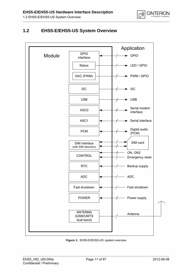
2.2.1 Antenna Interface Specifications
Table 8: Return loss in the active band
State of module Return loss of module Recommended return loss of application
Receive > 8dB > 12dB
Transmit not applicable > 12dB
Table 9: RF Antenna interface GSM / UMTS1
Parameter Conditions Min. Typical Max. Unit
UMTS/HSPA connectivity Band I, II, V, VIII
Receiver Input Sensitivity @ ARP
UMTS 850 Band V -104.7/ -106.7
-110 dBm
UMTS 900 Band VIII -103.7 -110 dBm
UMTS 1900 Band II -104.7 -109 dBm
UMTS 2100 Band I -106.7 -110 dBm
RF Power @ ARP with 50Ohm LoadBoard temperature <85°C
UMTS 850 Band V +21 +24 +25 dBm
UMTS 900 Band VIII +21 +24 +25 dBm
UMTS 1900 Band II +21 +24 +25 dBm
UMTS 2100 Band I +21 +24 +25 dBm
GPRS coding schemes Class 12, CS1 to CS4
EGPRS Class 12, MCS1 to MCS9
GSM Class Small MS
Static Receiver input Sensi-tivity @ ARP
GSM 850 / E-GSM 900 -102 -109 dBm
GSM 1800 / GSM 1900 -102 -108 dBm
RF Power @ ARP with 50Ohm Load
GSM GSM 850 / E-GSM 900 TBD. dBm
GSM 1800 / GSM 1900 TBD. dBm
EHS5-E/EHS5-US Hardware Interface Description2.2 RF Antenna Interface50
EHS5_HID_v00.000a Page 39 of 97 2012-06-08Confidential / Preliminary
RF Power @ ARP with 50Ohm Load, (ROPR = 4, i.e. no reduc-tion)
GPRS, 1 TX GSM 850 / E-GSM 900 TBD. dBm
GSM 1800 / GSM 1900 TBD. dBm
EDGE, 1 TX GSM 850 / E-GSM 900 TBD. dBm
GSM 1800 / GSM 1900 TBD. dBm
GPRS, 2 TX GSM 850 / E-GSM 900 TBD. dBm
GSM 1800 / GSM 1900 TBD. dBm
EDGE, 2 TX GSM 850 / E-GSM 900 TBD. dBm
GSM 1800 / GSM 1900 TBD. dBm
GPRS, 3 TX GSM 850 / E-GSM 900 TBD. dBm
GSM 1800 / GSM 1900 TBD. dBm
EDGE, 3 TX GSM 850 / E-GSM 900 TBD. dBm
GSM 1800 / GSM 1900 TBD. dBm
GPRS, 4 TX GSM 850 / E-GSM 900 TBD. dBm
GSM 1800 / GSM 1900 TBD. dBm
EDGE, 4 TX GSM 850 / E-GSM 900 TBD. dBm
GSM 1800 / GSM 1900 TBD. dBm
RF Power @ ARPwith 50Ohm Load,(ROPR = 5)
GPRS, 1 TX GSM 850 / E-GSM 900 TBD. dBm
GSM 1800 / GSM 1900 TBD. dBm
EDGE, 1 TX GSM 850 / E-GSM 900 TBD. dBm
GSM 1800 / GSM 1900 TBD. dBm
GPRS, 2 TX GSM 850 / E-GSM 900 TBD. dBm
GSM 1800 / GSM 1900 TBD. dBm
EDGE, 2 TX GSM 850 / E-GSM 900 TBD. dBm
GSM 1800 / GSM 1900 TBD. dBm
GPRS, 3 TX GSM 850 / E-GSM 900 TBD. dBm
GSM 1800 / GSM 1900 TBD. dBm
EDGE, 3 TX GSM 850 / E-GSM 900 TBD. dBm
GSM 1800 / GSM 1900 TBD. dBm
GPRS, 4 TX GSM 850 / E-GSM 900 TBD. dBm
GSM 1800 / GSM 1900 TBD. dBm
EDGE, 4 TX GSM 850 / E-GSM 900 TBD. dBm
GSM 1800 / GSM 1900 TBD. dBm
Table 9: RF Antenna interface GSM / UMTS1
Parameter Conditions Min. Typical Max. Unit

EHS5-E/EHS5-US Hardware Interface Description2.2 RF Antenna Interface50
EHS5_HID_v00.000a Page 40 of 97 2012-06-08Confidential / Preliminary
RF Power @ ARPwith 50Ohm Load,(ROPR = 6)
GPRS, 1 TX GSM 850 / E-GSM 900 TBD. dBm
GSM 1800 / GSM 1900 TBD. dBm
EDGE, 1 TX GSM 850 / E-GSM 900 TBD. dBm
GSM 1800 / GSM 1900 TBD. dBm
GPRS, 2 TX GSM 850 / E-GSM 900 TBD. dBm
GSM 1800 / GSM 1900 TBD. dBm
EDGE, 2 TX GSM 850 / E-GSM 900 TBD. dBm
GSM 1800 / GSM 1900 TBD. dBm
GPRS, 3 TX GSM 850 / E-GSM 900 TBD. dBm
GSM 1800 / GSM 1900 TBD. dBm
EDGE, 3 TX GSM 850 / E-GSM 900 TBD. dBm
GSM 1800 / GSM 1900 TBD. dBm
GPRS, 4 TX GSM 850 / E-GSM 900 TBD. dBm
GSM 1800 / GSM 1900 TBD. dBm
EDGE, 4 TX GSM 850 / E-GSM 900 TBD. dBm
GSM 1800 / GSM 1900 TBD. dBm
RF Power @ ARPwith 50Ohm Load,(ROPR = 7)
GPRS, 1 TX GSM 850 / E-GSM 900 TBD. dBm
GSM 1800 / GSM 1900 TBD. dBm
EDGE, 1 TX GSM 850 / E-GSM 900 TBD. dBm
GSM 1800 / GSM 1900 TBD. dBm
GPRS, 2 TX GSM 850 / E-GSM 900 TBD. dBm
GSM 1800 / GSM 1900 TBD. dBm
EDGE, 2 TX GSM 850 / E-GSM 900 TBD. dBm
GSM 1800 / GSM 1900 TBD. dBm
GPRS, 3 TX GSM 850 / E-GSM 900 TBD. dBm
GSM 1800 / GSM 1900 TBD. dBm
EDGE, 3 TX GSM 850 / E-GSM 900 TBD. dBm
GSM 1800 / GSM 1900 TBD. dBm
GPRS, 4 TX GSM 850 / E-GSM 900 TBD. dBm
GSM 1800 / GSM 1900 TBD. dBm
EDGE, 4 TX GSM 850 / E-GSM 900 TBD. dBm
GSM 1800 / GSM 1900 TBD. dBm
Table 9: RF Antenna interface GSM / UMTS1
Parameter Conditions Min. Typical Max. Unit

EHS5-E/EHS5-US Hardware Interface Description2.2 RF Antenna Interface50
EHS5_HID_v00.000a Page 41 of 97 2012-06-08Confidential / Preliminary
RF Power @ ARPwith 50Ohm Load,(ROPR = 8, i.e. maximum reduction)
GPRS, 1 TX GSM 850 / E-GSM 900 TBD. dBm
GSM 1800 / GSM 1900 TBD. dBm
EDGE, 1 TX GSM 850 / E-GSM 900 TBD. dBm
GSM 1800 / GSM 1900 TBD. dBm
GPRS, 2 TX GSM 850 / E-GSM 900 TBD. dBm
GSM 1800 / GSM 1900 TBD. dBm
EDGE, 2 TX GSM 850 / E-GSM 900 TBD. dBm
GSM 1800 / GSM 1900 TBD. dBm
GPRS, 3 TX GSM 850 / E-GSM 900 TBD. dBm
GSM 1800 / GSM 1900 TBD. dBm
EDGE, 3 TX GSM 850 / E-GSM 900 TBD. dBm
GSM 1800 / GSM 1900 TBD. dBm
GPRS, 4 TX GSM 850 / E-GSM 900 TBD. dBm
GSM 1800 / GSM 1900 TBD. dBm
EDGE, 4 TX GSM 850 / E-GSM 900 TBD. dBm
GSM 1800 / GSM 1900 TBD. dBm
1. Please note that the listed frequency bands apply as follows: - EHS5-E: GSM/GPRS 900/1800MHz; UMTS/HSPA+: 900/2100MHz (Band I / VIII)- EHS5-US: GSM/GPRS: 850/1900MHz; UMTS/HSPA+: 850/1900MHz (Band II / V)
Table 9: RF Antenna interface GSM / UMTS1
Parameter Conditions Min. Typical Max. Unit

EHS5-E/EHS5-US Hardware Interface Description2.2 RF Antenna Interface50
EHS5_HID_v00.000a Page 42 of 97 2012-06-08Confidential / Preliminary
2.2.2 Antenna Installation
The antenna is connected by soldering the antenna pad (RF_OUT, i.e., pad #59) and its neigh-boring ground pads (GND, i.e., pads #58 and #60) directly to the application’s PCB. The anten-na pad is the antenna reference point (ARP) for EHS5-E/EHS5-US. All RF data specified throughout this document is related to the ARP.
Figure 19: Antenna pads (bottom view)
The distance between the antenna RF_OUT pad (#59) and its neighboring GND pads (#58, #60) has been optimized for best possible impedance. On the application PCB, special atten-tion should be paid to these 3 pads, in order to prevent mismatch.
The wiring of the antenna connection line, starting from the antenna pad to the application an-tenna should result in a 50 line impedance. Line width and distance to the GND plane needs to be optimized with regard to the PCB’s layer stack. Some examples are given in Section 2.2.3.
To prevent receiver desensitization due to interferences generated by fast transients like high speed clocks on the application PCB, it is recommended to realize the antenna connection line using embedded Stripline rather than Micro-Stripline technology. Please see Section 2.2.3.1 for an example.
For type approval purposes, the use of a 50 coaxial antenna connector (U.FL-R-SMT) might be necessary. In this case the U.FL-R-SMT connector should be placed as close as possible to EHS5-E/EHS5-US‘s antenna pad.
53
65
64
63
62
61
60
59
58
57
56
55
54
66
33
21
22
23
24
25
26
27
28
29
30
31
32
20
106
9291
9897969594
9089
85 86
93
74
99
87 88
8483
7978777675
8281
80
727170696867
105104103102101100
73
44
19181716151413121110987654321
343536373839404142434546474849505152
GND
GND
RF_OUT

EHS5-E/EHS5-US Hardware Interface Description2.2 RF Antenna Interface50
EHS5_HID_v00.000a Page 43 of 97 2012-06-08Confidential / Preliminary
2.2.3 RF Line Routing Design
2.2.3.1 Line Arrangement Examples
Several dedicated tools are available to calculate line arrangements for specific applicationsand PCB materials - for example from http://www.polarinstruments.com/ (commercial software)or from http://web.awrcorp.com/Usa/Products/Optional-Products/TX-Line/ (free software).
Embedded StriplineThis figure below shows a line arrangement example for embedded stripline with 65µm FR4 prepreg (type: 1080) and 710µm FR4 core (4-layer PCB).
Figure 20: Embedded Stripline with 65µm prepreg (1080) and 710µm core

EHS5-E/EHS5-US Hardware Interface Description2.2 RF Antenna Interface50
EHS5_HID_v00.000a Page 44 of 97 2012-06-08Confidential / Preliminary
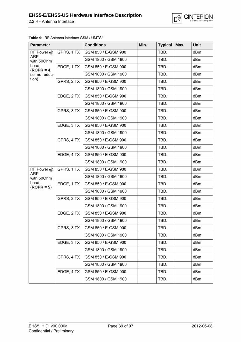
Micro-StriplineThis section gives two line arrangement examples for micro-stripline.
• Micro-Stripline on 1.0mm Standard FR4 2-Layer PCBThe following two figures show examples with different values for D1 (ground strip separa-tion).
Figure 21: Micro-Stripline on 1.0mm standard FR4 2-layer PCB - example 1
Antenna line
Ground line
Ground line
Application board
EHS5-E/EHS5-US Hardware Interface Description2.2 RF Antenna Interface50
EHS5_HID_v00.000a Page 45 of 97 2012-06-08Confidential / Preliminary
Figure 22: Micro-Stripline on 1.0mm Standard FR4 PCB - example 2
Antenna line
Ground line
Ground line
Application board

EHS5-E/EHS5-US Hardware Interface Description2.2 RF Antenna Interface50
EHS5_HID_v00.000a Page 46 of 97 2012-06-08Confidential / Preliminary
• Micro-Stripline on 1.5mm Standard FR4 2-Layer PCBThe following two figures show examples with different values for D1 (ground strip separa-tion).
Figure 23: Micro-Stripline on 1.5mm Standard FR4 PCB - example 1
Antenna line
Ground line
Ground line
Application board

EHS5-E/EHS5-US Hardware Interface Description2.2 RF Antenna Interface50
EHS5_HID_v00.000a Page 47 of 97 2012-06-08Confidential / Preliminary
Figure 24: Micro-Stripline on 1.5mm Standard FR4 PCB - example 2
Antenna line
Ground line
Ground line
Application board

EHS5-E/EHS5-US Hardware Interface Description2.2 RF Antenna Interface50
EHS5_HID_v00.000a Page 48 of 97 2012-06-08Confidential / Preliminary
2.2.3.2 Routing Example
Interface to RF ConnectorFigure 25 shows the connection of the module‘s antenna pad with an application PCB‘s coaxial antenna connector. Please note that the EHS5-E/EHS5-US bottom plane appears mirrored, since it is viewed from EHS5-E/EHS5-US top side. By definition the top of customer's board shall mate with the bottom of the EHS5-E/EHS5-US module.
Figure 25: Routing to application‘s RF connector - top view
Pad 1
EHS5-E/EHS5-US Hardware Interface Description2.3 Sample Application50
EHS5_HID_v00.000a Page 49 of 97 2012-06-08Confidential / Preliminary
2.3 Sample Application
Figure 26 shows a typical example of how to integrate a EHS5-E/EHS5-US module with an ap-plication. Usage of the various host interfaces depends on the desired features of the applica-tion.
Because of the very low power consumption design, current flowing from any other source intothe module circuit must be avoided, for example reverse current from high state external controllines. Therefore, the controlling application must be designed to prevent reverse current flow.Otherwise there is the risk of undefined states of the module during startup and shutdown oreven of damaging the module.
Because of the high RF field density inside the module, it cannot be guaranteed that no selfinterference might occur, depending on frequency and the applications grounding concept. ex-cluded that in some applications dependant on the grounding concept of the customer. The po-tential interferers may be minimized by placing small capacitors (47pF) at suspected lines (e.g.RXD0, RXT0, VDDLP, and ON).
While developing SMT applications it is strongly recommended to provide test pointsfor certain signals resp. lines to and from the module - for debug and/or test purposes.The SMT application should allow for an easy access to these signals. For details onhow to implement test points see [3].
The EMC measures are best practice recommendations. In fact, an adequate EMC strategy foran individual application is very much determined by the overall layout and, especially, the po-sition of components. For example, mounting the internal acoustic transducers directly on thePCB eliminates the need to use the ferrite beads shown in the sample schematic.
Please note that EHS5-E/EHS5-US is not intended for use with cables longer than 3m.
DisclaimerNo warranty, either stated or implied, is provided on the sample schematic diagram shown inFigure 26 and the information detailed in this section. As functionality and compliance with na-tional regulations depend to a great amount on the used electronic components and the indi-vidual application layout manufacturers are required to ensure adequate design and operatingsafeguards for their products using EHS5-E/EHS5-US modules.
EHS5-E/EHS5-US Hardware Interface Description2.3 Sample Application50
EHS5_HID_v00.000a Page 50 of 97 2012-06-08Confidential / Preliminary
Figure 26: Schematic diagram of EHS5-E/EHS5-US sample application
TBD.

EHS5-E/EHS5-US Hardware Interface Description3 Operating Characteristics69
EHS5_HID_v00.000a Page 51 of 97 2012-06-08Confidential / Preliminary
3 Operating Characteristics
3.1 Operating Modes
The table below briefly summarizes the various operating modes referred to throughout the document.
Table 10: Overview of operating modes
Mode Function
Normal operation
GSM / GPRS / UMTS / HSPA SLEEP
Power saving set automatically when no call is in progress and the USB connection is suspended by host or not present and no active commu-nication via ASC0.
GSM / GPRS / UMTS / HSPA IDLE
Power saving disabled or an USB connection not suspended, but no call in progress.
GSM TALK/GSM DATA
Connection between two subscribers is in progress. Power consump-tion depends on the GSM network coverage and several connection settings (e.g. DTX off/on, FR/EFR/HR, hopping sequences and antenna connection). The following applies when power is to be mea-sured in TALK_GSM mode: DTX off, FR and no frequency hopping.
GPRS DATA GPRS data transfer in progress. Power consumption depends on net-work settings (e.g. power control level), uplink / downlink data rates and GPRS configuration (e.g. used multislot settings).
EGPRS DATA EGPRS data transfer in progress. Power consumption depends on net-work settings (e.g. power control level), uplink / downlink data rates and EGPRS configuration (e.g. used multislot settings).
UMTS TALK/UMTS DATA
UMTS data transfer in progress. Power consumption depends on net-work settings (e.g. TPC Pattern) and data transfer rate.
HSPA DATA HSPA data transfer in progress. Power consumption depends on net-work settings (e.g. TPC Pattern) and data transfer rate.
Power Down
Normal shutdown after sending the power down command. Only a voltage regulator is active for powering the RTC. Software is not active. Interfaces are not accessible. Operat-ing voltage (connected to BATT+) remains applied.
Airplane mode
Airplane mode shuts down the radio part of the module, causes the module to log off from the GSM/GPRS network and disables all AT commands whose execution requires a radio connection.Airplane mode can be controlled by AT command (see [1]).

EHS5-E/EHS5-US Hardware Interface Description3.2 Power Up/Power Down Scenarios69
EHS5_HID_v00.000a Page 52 of 97 2012-06-08Confidential / Preliminary
3.2 Power Up/Power Down Scenarios
In general, be sure not to turn on EHS5-E/EHS5-US while it is beyond the safety limits of volt-age and temperature stated in Section 2.1.2.1. EHS5-E/EHS5-US would immediately switch off after having started and detected these inappropriate conditions. In extreme cases this can cause permanent damage to the module.
3.2.1 Turn on EHS5-E/EHS5-US
EHS5-E/EHS5-US can be started as described in the following sections:• Hardware driven switch on by ON line: Starts Normal mode (see Section 3.2.1.1).• Hardware driven switch on by ON2 line: Starts Normal mode (see Section 3.2.1.2).
3.2.1.1 Switch on EHS5-E/EHS5-US Using ON Signal
When the operating voltage BATT+ is applied, EHS5-E/EHS5-US can be switched on by meansof the ON signal.
The ON signal is an edge triggered signal and only allows the input voltage level of the VDDLPsignal. The module starts into normal mode on detecting the rising edge of the ON signal.
The following Figure 27 shows an example for a switch-on circuit.
Figure 27: ON circuit sample
It is recommended to set a serial 1kOhm resistor between the ON circuit and the external ca-pacitor or battery at the VDDLP power supply. This serial resistor protection is necessary incase the capacitor or battery has low power (is empty). Typical values for the resistors shownin Figure 27 are R1=150k and R2=22k, depending on the current gain of the employed PNPtransistor.
VDDLP
ON
1k
+R1
R2
Option 1 Option 2

EHS5-E/EHS5-US Hardware Interface Description3.2 Power Up/Power Down Scenarios69
EHS5_HID_v00.000a Page 53 of 97 2012-06-08Confidential / Preliminary
Please note that the ON signal is an edge triggered signal. This implies that a micro-secondhigh pulse on the signal line (typically 60µs) suffices to almost immediately switch on the mod-ule, as shown in Figure 28. Also, the ON signal must be low for at least 100µs before triggeringthe high impulse.
Figure 28: ON timing
BATT+
ON
EMERG_RST
V180
VCORE
VDDLP
~ 26ms
~ 5ms
~ 7ms
Rising edge starts up the module
>100µs

EHS5-E/EHS5-US Hardware Interface Description3.2 Power Up/Power Down Scenarios69
EHS5_HID_v00.000a Page 54 of 97 2012-06-08Confidential / Preliminary
3.2.1.2 Switch on EHS5-E/EHS5-US Using ON2 Signal
In case the ON2 signal is permanently connected to ground (i.e., low level) the module will startup if the operating voltage BATT+ is applied with a rise time faster than 24ms.
The following Figure 29 shows the startup behavior if employing the ON2 signal.
Figure 29: ON2 timing
3.2.2 Restart EHS5-E/EHS5-US
After startup EHS5-E/EHS5-US can be re-started as described in the following sections:• Software controlled reset by AT+CFUN command: Starts Normal mode (see Section
3.2.2.1).• Hardware controlled reset by EMERG_RST line: Starts Normal mode (see Section 3.2.2.2)
3.2.2.1 Restart EHS5-E/EHS5-US via AT+CFUN Command
To reset and restart the EHS5-E/EHS5-US module use the command AT+CFUN. See [1] for details.
BATT+
ON2
EMERG_RST
V180
VCORE
VDDLP
<= 24ms
~ 5ms
~ 7ms
~ 26ms
Start up with continuous ON2 signal
BATT+ rise time
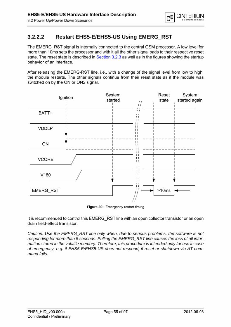
EHS5-E/EHS5-US Hardware Interface Description3.2 Power Up/Power Down Scenarios69
EHS5_HID_v00.000a Page 55 of 97 2012-06-08Confidential / Preliminary
3.2.2.2 Restart EHS5-E/EHS5-US Using EMERG_RST
The EMERG_RST signal is internally connected to the central GSM processor. A low level formore than 10ms sets the processor and with it all the other signal pads to their respective resetstate. The reset state is described in Section 3.2.3 as well as in the figures showing the startupbehavior of an interface.
After releasing the EMERG-RST line, i.e., with a change of the signal level from low to high,the module restarts. The other signals continue from their reset state as if the module wasswitched on by the ON or ON2 signal.
Figure 30: Emergency restart timing
It is recommended to control this EMERG_RST line with an open collector transistor or an opendrain field-effect transistor.
Caution: Use the EMERG_RST line only when, due to serious problems, the software is notresponding for more than 5 seconds. Pulling the EMERG_RST line causes the loss of all infor-mation stored in the volatile memory. Therefore, this procedure is intended only for use in caseof emergency, e.g. if EHS5-E/EHS5-US does not respond, if reset or shutdown via AT com-mand fails.
BATT+
ON
EMERG_RST
VCORE
V180
VDDLP
>10ms
System started
System started again
Resetstate
Ignition

EHS5-E/EHS5-US Hardware Interface Description3.2 Power Up/Power Down Scenarios69
EHS5_HID_v00.000a Page 56 of 97 2012-06-08Confidential / Preliminary
3.2.3 Signal States after Startup
Table 11 lists the states each interface signal passes through during reset and firmware initial-ization.
The reset state is reached with the rising edge of the EMERG_RST signal - either after a normalmodule startup (see Section 3.2.1.1) or after a reset (see Section 3.2.2.2). After the reset statehas been reached the firmware initialization state begins. The firmware initialization is complet-ed as soon as the ASC0 interface lines CTS0, DSR0 and RING0 as well as the ASC1 interfaceline CTS1 have turned low (see Section 2.1.4 and Section 2.1.5). Now, the module is ready toreceive and transmit data.
Abbreviations used in above Table 11:
Table 11: Signal states
Signal name Reset state Firmware initialization
CCIN T / PD I / 100k PD
CCRST L O / L
CCIO L O / L
CCCLK L O / L
RXD0 T / PU O / H
TXD0 T / PD I
CTS0 T / PU O / H
RTS0 T / PU I / PD
RING0 T / PD O / H
DTR0 T / PD I
DCD0 T / PD O / H
DSR0 T / PD O / H
RXD1 T / PD O / H
TXD1 T / PD I
CTS1 T / PD O / H
RTS1 T / PD I / PD
SCLK T / PD O / L
RXDDAI T / PD I
TXDDAI T / PD O / L
TFSDAI T / PD O / L
FAST_SHTDWN T / PD T / PD
GPIO5 / LED O / L T / PD
GPIO6 / PWM2 O / L T / PD
GPIO7 / PWM1 O / L T / PD
GPIO8 O / L T / PD
I2CCLK T T / OD
I2CDAT T T / OD
L = Low levelH = High levelL/H = Low or high levelT = Tristate
I = InputO = OutputOD = Open DrainPD = Pull down, 200µA at 1.9VPU = Pull up, -240µA at 0V

EHS5-E/EHS5-US Hardware Interface Description3.2 Power Up/Power Down Scenarios69
EHS5_HID_v00.000a Page 57 of 97 2012-06-08Confidential / Preliminary
3.2.4 Turn off EHS5-E/EHS5-US
To switch the module off the following procedures may be used: • Normal shutdown procedure: Software controlled by sending an AT command over the
serial application interface. See Section 3.2.4.1.• Automatic shutdown: See Section 3.2.5
- Takes effect if under- or overvoltage is detected. - Takes effect if EHS5-E/EHS5-US board temperature exceeds a critical limit.
3.2.4.1 Switch off EHS5-E/EHS5-US Using AT Command
The best and safest approach to powering down EHS5-E/EHS5-US is to issue the appropriateAT command. This procedure lets EHS5-E/EHS5-US log off from the network and allows thesoftware to enter into a secure state and safe data before disconnecting the power supply. Themode is referred to as Power Down mode. In this mode, only the RTC stays active.
Be sure not to disconnect the operating voltage VBATT+ before V180 pad has gone low. Other-wise you run the risk of losing data.
While EHS5-E/EHS5-US is in Power Down mode the application interface is switched off andmust not be fed from any other voltage source. Therefore, your application must be designedto avoid any current flow into any digital pads of the application interface.
Figure 31: Switch off behavior
BATT+
ON
VCORE
V180
VDDLP
AT+CPWROFF System power down procedure Power down
EMERG_RST
ON2

EHS5-E/EHS5-US Hardware Interface Description3.2 Power Up/Power Down Scenarios69
EHS5_HID_v00.000a Page 58 of 97 2012-06-08Confidential / Preliminary
3.2.5 Automatic Shutdown
Automatic shutdown1 takes effect if any of the following events occurs:• the EHS5-E/EHS5-US board is exceeding the critical limits of overtemperature or under-
temperature• undervoltage or overvoltage is detected
The automatic shutdown procedure is equivalent to the power-down initiated with an AT com-mand, i.e. EHS5-E/EHS5-US logs off from the network and the software enters a secure stateavoiding loss of data.
3.2.5.1 Thermal Shutdown
The board temperature is constantly monitored by an internal NTC resistor located on the PCB.The values detected by the NTC resistor are measured directly on the board and therefore, arenot fully identical with the ambient temperature.
To be continued...
3.2.5.2 Undervoltage Shutdown
To be continued
3.2.5.3 Overvoltage Shutdown
To be continued.
1. Not yet implemented.

EHS5-E/EHS5-US Hardware Interface Description3.3 Power Saving69
EHS5_HID_v00.000a Page 59 of 97 2012-06-08Confidential / Preliminary
3.3 Power Saving
To be continued.

EHS5-E/EHS5-US Hardware Interface Description3.4 Power Supply69
EHS5_HID_v00.000a Page 60 of 97 2012-06-08Confidential / Preliminary
3.4 Power Supply
EHS5-E/EHS5-US needs to be connected to a power supply at the SMT application interface (2 lines each BATT+ and GND).
The power supply of EHS5-E/EHS5-US has to be a single voltage source at BATT+. It must be able to provide the peak current during the uplink transmission.
All the key functions for supplying power to the device are handled by the power management section of the analog controller. This IC provides the following features:
• Stabilizes the supply voltages for the baseband using low drop linear voltage regulators anda DC-DC step down switching regulator.
• Switches the module's power voltages for the power-up and -down procedures.• SIM switch to provide SIM power supply.
3.4.1 Power Supply Ratings
Table 12: Power supply ratings1 (TBD.)
Description Conditions Min Typ Max Unit
BATT+ Supply voltage Directly measured at Module.Voltage must stay within the min/max values, including voltage drop, ripple, spikes
3.3 3.8 4.5 V
Maximum allowed voltage drop dur-ing transmit burst
Normal condition, power control level for Pout max
mV
Voltage ripple Normal condition, power control level for Pout max@ f <= 250 kHz@ f > 250 kHz
mVppmVpp
IVDDLP @ 3V
OFF State supply current
RTC backup @ BATT+ = 0V µA

EHS5-E/EHS5-US Hardware Interface Description3.4 Power Supply69
EHS5_HID_v00.000a Page 61 of 97 2012-06-08Confidential / Preliminary
IBATT+ 2 OFF State supply
current POWER DOWN µA
Average GSM / GPRS supply cur-rent
SLEEP3 (USB Suspend or USB discon-nected and no communication via ASC0) @ DRX=9
mA
SLEEP3 (USB Suspend or USB discon-nected and no communication via ASC0) @ DRX=5
mA
SLEEP3 (USB Suspend or USB discon-nected and no communication via ASC0) @ DRX=2
mA
IDLE (USB disconnected, UART active) @ DRX=2
mA
IDLE (USB active) @ DRX=2 mA
Voice Call GSM850/900; PCL=5 mA
GPRS Data transfer GSM850/900; PCL=5; 1Tx/4Rx
ROPR=8 (max. reduction)
mA
ROPR=4 (no reduction)
mA
GPRS Data transfer GSM850/900; PCL=5; 2Tx/3Rx
ROPR=8 (max. reduction)
mA
ROPR=4 (no reduction)
mA
GPRS Data transfer GSM850/900; PCL=5; 4Tx/1Rx
ROPR=8 (max. reduction)
mA
ROPR=4 (no reduction)
mA
Table 12: Power supply ratings1 (TBD.)
Description Conditions Min Typ Max Unit

EHS5-E/EHS5-US Hardware Interface Description3.4 Power Supply69
EHS5_HID_v00.000a Page 62 of 97 2012-06-08Confidential / Preliminary
IBATT+ 2 Average GSM /
GPRS supply current
EDGE Data transfer GSM850/900; PCL=5; 1Tx/4Rx
ROPR=8 (max. reduction)
mA
ROPR=4 (no reduction)
mA
EDGE Data transfer GSM850/900; PCL=5; 2Tx/3Rx
ROPR=8 (max. reduction)
mA
ROPR=4 (no reduction)
mA
EDGE Data transfer GSM850/900; PCL=5; 4Tx/1Rx
ROPR=8 (max. reduction)
mA
ROPR=4 (no reduction)
mA
Voice Call GSM1800/1900; PCL=0 mA
GPRS Data transfer GSM1800/1900; PCL=0; 1Tx/4Rx
ROPR=8 (max. reduction)
mA
ROPR=4 (no reduction)
mA
GPRS Data transfer GSM1800/1900; PCL=0; 2Tx/3Rx
ROPR=8 (max. reduction)
mA
ROPR=4 (no reduction)
mA
GPRS Data transfer GSM1800/1900; PCL=0; 4Tx/1Rx
ROPR=8 (max. reduction)
mA
ROPR=4 (no reduction)
mA
EDGE Data transfer GSM1800/1900; PCL=0; 1Tx/4Rx
ROPR=8 (max. reduction)
mA
ROPR=4 (no reduction)
mA
EDGE Data transfer GSM1800/1900; PCL=0; 2Tx/3Rx
ROPR=8 (max. reduction)
mA
ROPR=4 (no reduction)
mA
EDGE Data transfer GSM1800/1900; PCL=0; 4Tx/1Rx
ROPR=8 (max. reduction)
mA
ROPR=4 (no reduction)
mA
Peak current dur-ing GSM transmit burst
VOICE Call GSM850/900; PCL=5 A
VOICE Call GSM1800/1900; PCL=0 A
IBATT+ 2 Average WCDMA
supply currentSLEEP3 (USB Suspend or USB discon-nected and no communication via ASC0) @ DRX=9
mA
SLEEP3 (USB Suspend or USB discon-nected and no communication via ASC0) @ DRX=8
mA
Table 12: Power supply ratings1 (TBD.)
Description Conditions Min Typ Max Unit

EHS5-E/EHS5-US Hardware Interface Description3.4 Power Supply69
EHS5_HID_v00.000a Page 63 of 97 2012-06-08Confidential / Preliminary
SLEEP3 (USB Suspend or USB discon-nected and no communication via ASC0) @ DRX=6
mA
IDLE (USB disconnected, UART active) @ DRX=6
mA
IDLE (USB active) @ DRX=6 mA
Voice Call Band I; 24dBm mA
Voice Call Band II; 24dBm mA
Voice Call Band V; 24dBm mA
Voice Call Band VIII; 24dBm mA
UMTS Data transfer Band I @+24dBm mA
UMTS Data transfer Band II @+24dBm mA
UMTS Data transfer Band V @+24dBm mA
UMTS Data transfer Band VIII @+24dBm mA
HSPA Data transfer Band I @+24dBm mA
HSPA Data transfer Band II @+24dBm mA
HSPA Data transfer Band V @+24dBm mA
HSPA Data transfer Band VIII @+24dBm mA
1. Please note that the listed frequency bands apply as follows: - EHS5-E: GSM/GPRS 900/1800MHz; UMTS/HSPA+: 900/2100MHz (Band I / VIII)- EHS5-US: GSM/GPRS: 850/1900MHz; UMTS/HSPA+: 850/1900MHz (Band II / V
2. With an impedance of ZLOAD=50Ohm at the antenna connector.3. Measurements start 6 minutes after switching ON the module,
Averaging times: SLEEP mode - 3 minutes, transfer modes - 1.5 minutesCommunication tester settings: no neighbour cells, no cell reselection etc., RMC (reference measu-rement channel)
Table 12: Power supply ratings1 (TBD.)
Description Conditions Min Typ Max Unit
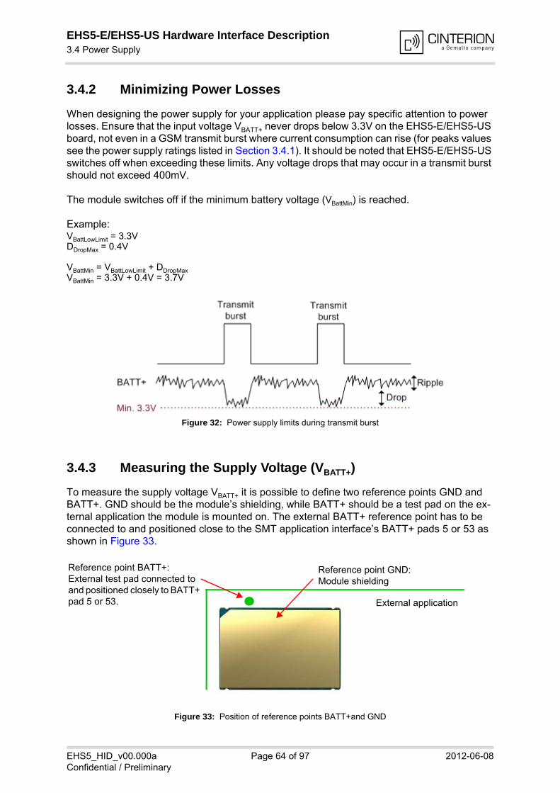
EHS5-E/EHS5-US Hardware Interface Description3.4 Power Supply69
EHS5_HID_v00.000a Page 64 of 97 2012-06-08Confidential / Preliminary
3.4.2 Minimizing Power Losses
When designing the power supply for your application please pay specific attention to power losses. Ensure that the input voltage VBATT+ never drops below 3.3V on the EHS5-E/EHS5-US board, not even in a GSM transmit burst where current consumption can rise (for peaks values see the power supply ratings listed in Section 3.4.1). It should be noted that EHS5-E/EHS5-US switches off when exceeding these limits. Any voltage drops that may occur in a transmit burst should not exceed 400mV.
The module switches off if the minimum battery voltage (VBattMin) is reached.
Example: VBattLowLimit = 3.3VDDropMax = 0.4V
VBattMin = VBattLowLimit + DDropMaxVBattMin = 3.3V + 0.4V = 3.7V
Figure 32: Power supply limits during transmit burst
3.4.3 Measuring the Supply Voltage (VBATT+)
To measure the supply voltage VBATT+ it is possible to define two reference points GND and BATT+. GND should be the module’s shielding, while BATT+ should be a test pad on the ex-ternal application the module is mounted on. The external BATT+ reference point has to be connected to and positioned close to the SMT application interface’s BATT+ pads 5 or 53 as shown in Figure 33.
Figure 33: Position of reference points BATT+and GND
Reference point GND:Module shielding
Reference point BATT+:External test pad connected to and positioned closely to BATT+ pad 5 or 53. External application

EHS5-E/EHS5-US Hardware Interface Description3.5 Operating Temperatures69
EHS5_HID_v00.000a Page 65 of 97 2012-06-08Confidential / Preliminary
3.5 Operating Temperatures
Please note that the module’s lifetime, i.e., the MTTF (mean time to failure) may be reduced, ifoperated outside the extended temperature range.
See also Section 3.3 for information about the NTC for on-board temperature measurement,automatic thermal shutdown and alert messages.
Note that within the specified operating temperature ranges the board temperature may varyto a great extent depending on operating mode, used frequency band, radio output power andcurrent supply voltage.
Table 13: Board temperature
Parameter Min Typ Max Unit
Normal operation TBD. TBD. TBD. °C
Extended operation1
1. Extended operation allows normal mode speech calls or data transmission for limited time until automatic thermal shutdown takes effect. Within the extended temperature range (outside the normal operating temperature range) the specified electrical characteristics may be in- or decreased.
TBD. TBD. °C
Automatic shutdown2
Temperature measured on EHS5-E/EHS5-USboard
2. Due to temperature measurement uncertainty, a tolerance of ±3°C on the thresholds may occur.
<TBD. --- >TBD. °C
EHS5-E/EHS5-US Hardware Interface Description3.6 Electrostatic Discharge69
EHS5_HID_v00.000a Page 66 of 97 2012-06-08Confidential / Preliminary
3.6 Electrostatic Discharge
The GSM module is not protected against Electrostatic Discharge (ESD) in general. Conse-quently, it is subject to ESD handling precautions that typically apply to ESD sensitive compo-nents. Proper ESD handling and packaging procedures must be applied throughout theprocessing, handling and operation of any application that incorporates a EHS5-E/EHS5-USmodule.
Special ESD protection provided on EHS5-E/EHS5-US: An example for an enhanced ESD protection for the SIM interface is given in Section 2.1.6.1.
EHS5-E/EHS5-US has been tested according to group standard ETSI EN 301 489-1 (see Table21) and test standard EN 61000-4-2. Electrostatic values can be gathered from the followingtable.
Note: Please note that the values may vary with the individual application design. For example,it matters whether or not the application platform is grounded over external devices like a com-puter or other equipment, such as the Cinterion reference application described in Chapter 5.
3.6.1 Blocking against RF on Interface Lines
To reduce EMI issues there are serial resistors, or capacitors to GND, implemented on themodule for the ignition, emergency restart, and SIM interface lines (cp. Section 2.3). However,all other signal lines have no EMI measures on the module and there are no blocking measuresat the module’s interface to an external application.
Dependent on the specific application design, it might be useful to implement further EMI mea-sures on some signal lines at the interface between module and application. These measuresare described below.
There are five possible variants of EMI measures (A-E) that may be implemented betweenmodule and external application depending on the signal line (see Figure 34 and Table 15). Payattention not to exceed the maximum input voltages and prevent voltage overshots if using in-ductive EMC measures.
The maximum value of the serial resistor should be lower than 1kOhm on the signal line. Themaximum value of the capacitor should be lower than 50pF on the signal line. Please observethe electrical specification of the module interface and the application interface.
Table 14: Electrostatic values
Specification/Requirements Contact discharge Air discharge
EN 61000-4-2
Antenna interface 4kV 8kV
JEDEC JESD22-A114D (Human Body Model, Test conditions: 1.5 k, 100 pF)
ESD at the module 1kV n.a.

EHS5-E/EHS5-US Hardware Interface Description3.6 Electrostatic Discharge69
EHS5_HID_v00.000a Page 67 of 97 2012-06-08Confidential / Preliminary
Figure 34: EMI circuits
RB2B Application
EMI measures A C
B2B Application
GND
EMI measures B
R
C
B2B Application
GND
EMI measures C
LB2B Application
EMI measures D
L
C
B2B Application
GND
EMI measures E

EHS5-E/EHS5-US Hardware Interface Description3.6 Electrostatic Discharge69
EHS5_HID_v00.000a Page 68 of 97 2012-06-08Confidential / Preliminary
The following table lists for each signal line at the SMT application interface the EMI measuresthat may be implemented.
Table 15: EMI measures on the application interface
Signal name EMI measures Remark
A B C D E
CCIN x x
CCRST x The external capacitor should be not higher than 30pF. The value of the capacitor depends on the external application.CCIO x
CCCLK x
RXD0 x x x x x
TXD0 x x x x x
CTS0 x x x x x
RTS0 x
RING0 x
DTR0 x x x x x
DCD0 x x x x x
DSR0 x x x x x
RXD1 x x x x x
TXD1 x x x x x
CTS1 x x x x x
RTS1 x x x x x
GPIO5/LED x x x x x
GPIO6/PWM2 x x x x x
GPIO7/PWM1 x x x x x
GPIO8 x x x x x
I2CDAT x x The rising signal edge is reduced with an additional capacitor.
I2CCLK x x
V180 x x x
VCORE x x x

EHS5-E/EHS5-US Hardware Interface Description3.7 Reliability Characteristics69
EHS5_HID_v00.000a Page 69 of 97 2012-06-08Confidential / Preliminary
3.7 Reliability Characteristics
The test conditions stated below are an extract of the complete test specifications.
Table 16: Summary of reliability test conditions
Type of test Conditions Standard
Vibration Frequency range: 10-20Hz; acceleration: 5gFrequency range: 20-500Hz; acceleration: 20gDuration: 20h per axis; 3 axes
DIN IEC 60068-2-61
1. For reliability tests in the frequency range 20-500Hz the Standard’s acceleration reference value was increased to 20g.
Shock half-sinus Acceleration: 500gShock duration: 1msec1 shock per axis6 positions (± x, y and z)
DIN IEC 60068-2-27
Dry heat Temperature: +70 ±2°CTest duration: 16hHumidity in the test chamber: < 50%
EN 60068-2-2 Bb ETS 300 019-2-7
Temperature change (shock)
Low temperature: -40°C ±2°CHigh temperature: +85°C ±2°CChangeover time: < 30s (dual chamber system)Test duration: 1hNumber of repetitions: 100
DIN IEC 60068-2-14 Na
ETS 300 019-2-7
Damp heat cyclic High temperature: +55°C ±2°CLow temperature: +25°C ±2°CHumidity: 93% ±3%Number of repetitions: 6Test duration: 12h + 12h
DIN IEC 60068-2-30 Db
ETS 300 019-2-5
Cold (constant exposure)
Temperature: -40 ±2°CTest duration: 16h
DIN IEC 60068-2-1

EHS5-E/EHS5-US Hardware Interface Description4 Mechanical Dimensions, Mounting and Packaging84
EHS5_HID_v00.000a Page 70 of 97 2012-06-08Confidential / Preliminary
4 Mechanical Dimensions, Mounting and Packaging
4.1 Mechanical Dimensions of EHS5-E/EHS5-US
Figure 35 shows the top and bottom view of EHS5-E/EHS5-US and provides an overview of the board's mechanical dimensions. For further details see Figure 36.
Figure 35: EHS5-E/EHS5-US– top and bottom view
Product label
Top view
Bottom view

EHS5-E/EHS5-US Hardware Interface Description4.1 Mechanical Dimensions of EHS5-E/EHS5-US84
EHS5_HID_v00.000a Page 71 of 97 2012-06-08Confidential / Preliminary
Figure 36: Dimensions of EHS5-E/EHS5-US (all dimensions in mm)

EHS5-E/EHS5-US Hardware Interface Description4.2 Mounting EHS5-E/EHS5-US onto the Application Platform84
EHS5_HID_v00.000a Page 72 of 97 2012-06-08Confidential / Preliminary
4.2 Mounting EHS5-E/EHS5-US onto the Application Platform
This section describes how to mount EHS5-E/EHS5-US onto the PCBs (=printed circuit boards), including land pattern and stencil design, board-level characterization, soldering con-ditions, durability and mechanical handling. For more information on issues related to SMT module integration see also [3].
4.2.1 SMT PCB Assembly
4.2.1.1 Land Pattern and Stencil
The land pattern and stencil design as shown below is based on Cinterion characterizations for lead-free solder paste on a four-layer test PCB and a 110 respectively 150 micron thick stencil.
The land pattern given in Figure 37 reflects the module‘s pad layout, including signal pads and ground pads (for pad assignment see Section 2.1.1).
Figure 37: Land pattern (top view)
The stencil design illustrated in Figure 38 and Figure 39 is recommended by Cinterion as a result of extensive tests with Cinterion Daisy Chain modules.
The central ground pads are primarily intended for stabilizing purposes, and may show some more voids than the application interface pads at the module's rim. This is acceptable, since they are electrically irrelevant.
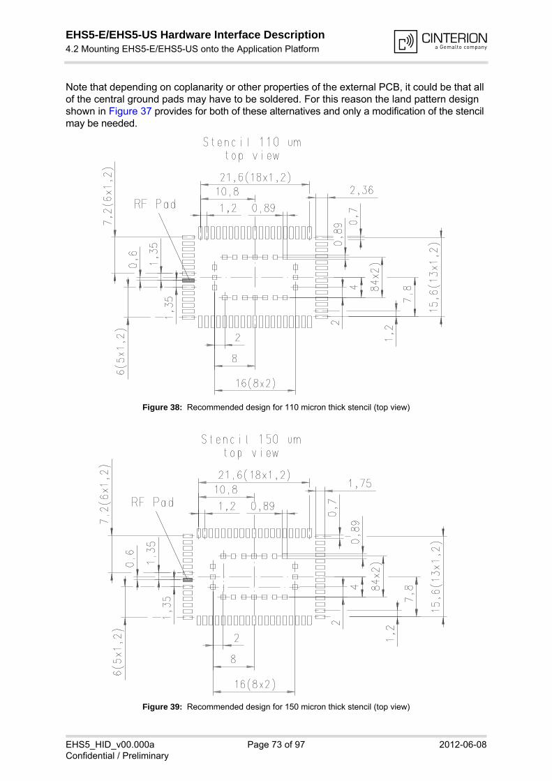
EHS5-E/EHS5-US Hardware Interface Description4.2 Mounting EHS5-E/EHS5-US onto the Application Platform84
EHS5_HID_v00.000a Page 73 of 97 2012-06-08Confidential / Preliminary
Note that depending on coplanarity or other properties of the external PCB, it could be that all of the central ground pads may have to be soldered. For this reason the land pattern design shown in Figure 37 provides for both of these alternatives and only a modification of the stencil may be needed.
Figure 38: Recommended design for 110 micron thick stencil (top view)
Figure 39: Recommended design for 150 micron thick stencil (top view)
EHS5-E/EHS5-US Hardware Interface Description4.2 Mounting EHS5-E/EHS5-US onto the Application Platform84
EHS5_HID_v00.000a Page 74 of 97 2012-06-08Confidential / Preliminary
4.2.1.2 Board Level Characterization
Board level characterization issues should also be taken into account if devising an SMT pro-cess.
Characterization tests should attempt to optimize the SMT process with regard to board level reliability. This can be done by performing the following physical tests on sample boards: Peel test, bend test, tensile pull test, drop shock test and temperature cycling. Sample surface mount checks are described in [3].
It is recommended to characterize land patterns before an actual PCB production, taking indi-vidual processes, materials, equipment, stencil design, and reflow profile into account. For land and stencil pattern design recommendations see also Section 4.2.1.1. Optimizing the solder stencil pattern design and print process is necessary to ensure print uniformity, to decrease sol-der voids, and to increase board level reliability.
Daisy chain modules for SMT characterization are available on request. For details refer to [3].
Generally, solder paste manufacturer recommendations for screen printing process parame-ters and reflow profile conditions should be followed. Maximum ratings are described in Section 4.2.3.
4.2.2 Moisture Sensitivity Level
EHS5-E/EHS5-US comprises components that are susceptible to damage induced by ab-sorbed moisture.
Cinterion’s EHS5-E/EHS5-US module complies with the latest revision of the IPC/JEDEC J-STD-020 Standard for moisture sensitive surface mount devices and is classified as MSL 4.
For additional MSL (=moisture sensitivity level) related information see Section 4.2.4 and Sec-tion 4.3.2.

EHS5-E/EHS5-US Hardware Interface Description4.2 Mounting EHS5-E/EHS5-US onto the Application Platform84
EHS5_HID_v00.000a Page 75 of 97 2012-06-08Confidential / Preliminary
4.2.3 Soldering Conditions and Temperature
4.2.3.1 Reflow Profile
Figure 40: Reflow Profile
Table 17: Reflow temperature ratings
Profile Feature Pb-Free Assembly
Preheat & SoakTemperature Minimum (TSmin)Temperature Maximum (TSmax)Time (tSmin to tSmax) (tS)
150°C200°C60-120 seconds
Average ramp up rate (TSmax to TP) 3K/second max.
Liquidous temperature (TL)Time at liquidous (tL)
217°C60-90 seconds
Peak package body temperature (TP) 245°C +0/-5°C
Time (tP) within 5 °C of the peak package body temperature (TP)
30 seconds max.
Average ramp-down rate (TP to TSmax) 6 K/second max.
Time 25°C to maximum temperature 8 minutes max.
TL
TP
tP
tL
tS
Preheat
t to maximum Time
Tem
pera
ture
TSmin
TSmax

EHS5-E/EHS5-US Hardware Interface Description4.2 Mounting EHS5-E/EHS5-US onto the Application Platform84
EHS5_HID_v00.000a Page 76 of 97 2012-06-08Confidential / Preliminary
4.2.3.2 Maximum Temperature and Duration
The following limits are recommended for the SMT board-level soldering process to attach the module:• A maximum module temperature of 245°C. This specifies the temperature as measured at
the module’s top side.• A maximum duration of 30 seconds at this temperature.
Please note that while the solder paste manufacturers' recommendations for best temperature and duration for solder reflow should generally be followed, the limits listed above must not be exceeded.
EHS5-E/EHS5-US is specified for one soldering cycle only. Once EHS5-US is removed from the application, the module will very likely be destroyed and cannot be soldered onto another application.

EHS5-E/EHS5-US Hardware Interface Description4.2 Mounting EHS5-E/EHS5-US onto the Application Platform84
EHS5_HID_v00.000a Page 77 of 97 2012-06-08Confidential / Preliminary
4.2.4 Durability and Mechanical Handling
4.2.4.1 Storage Conditions
EHS5-E/EHS5-US modules, as delivered in tape and reel carriers, must be stored in sealed, moisture barrier anti-static bags. The conditions stated below are only valid for modules in their original packed state in weather protected, non-temperature-controlled storage locations. Nor-mal storage time under these conditions is 12 months maximum.
Table 18: Storage conditions
Type Condition Unit Reference
Air temperature: LowHigh
-25+40
°C IPC/JEDEC J-STD-033A
Humidity relative: LowHigh
1090 at 40°C
%IPC/JEDEC J-STD-033A
Air pressure: LowHigh
70106
kPa IEC TR 60271-3-1: 1K4IEC TR 60271-3-1: 1K4
Movement of surrounding air 1.0 m/s IEC TR 60271-3-1: 1K4
Water: rain, dripping, icing and frosting
Not allowed --- ---
Radiation: SolarHeat
1120600
W/m2 ETS 300 019-2-1: T1.2, IEC 60068-2-2 BbETS 300 019-2-1: T1.2, IEC 60068-2-2 Bb
Chemically active substances Not recommended
IEC TR 60271-3-1: 1C1L
Mechanically active substances Not recommended
IEC TR 60271-3-1: 1S1
Vibration sinusoidal:DisplacementAccelerationFrequency range
1.552-9 9-200
mmm/s2
Hz
IEC TR 60271-3-1: 1M2
Shocks:Shock spectrumDurationAcceleration
semi-sinusoidal150
msm/s2
IEC 60068-2-27 Ea

EHS5-E/EHS5-US Hardware Interface Description4.2 Mounting EHS5-E/EHS5-US onto the Application Platform84
EHS5_HID_v00.000a Page 78 of 97 2012-06-08Confidential / Preliminary
4.2.4.2 Processing Life
EHS5-E/EHS5-US must be soldered to an application within 72 hours after opening the MBB (=moisture barrier bag) it was stored in.
As specified in the IPC/JEDEC J-STD-033 Standard, the manufacturing site processing the modules should have ambient temperatures below 30°C and a relative humidity below 60%.
4.2.4.3 Baking
Baking conditions are specified on the moisture sensitivity label attached to each MBB (see Figure 45 for details):• It is not necessary to bake EHS5-E/EHS5-US, if the conditions specified in Section 4.2.4.1
and Section 4.2.4.2 were not exceeded.• It is necessary to bake EHS5-E/EHS5-US, if any condition specified in Section 4.2.4.1 and
Section 4.2.4.2 was exceeded.
If baking is necessary, the modules must be put into trays that can be baked to at least 125°C. Devices should not be baked in tape and reel carriers at any temperature.
4.2.4.4 Electrostatic Discharge
ESD (=electrostatic discharge) may lead to irreversable damage for the module. It is therefore advisable to develop measures and methods to counter ESD and to use these to control the electrostatic environment at manufacturing sites.
Please refer to Section 3.6 for further information on electrostatic discharge.
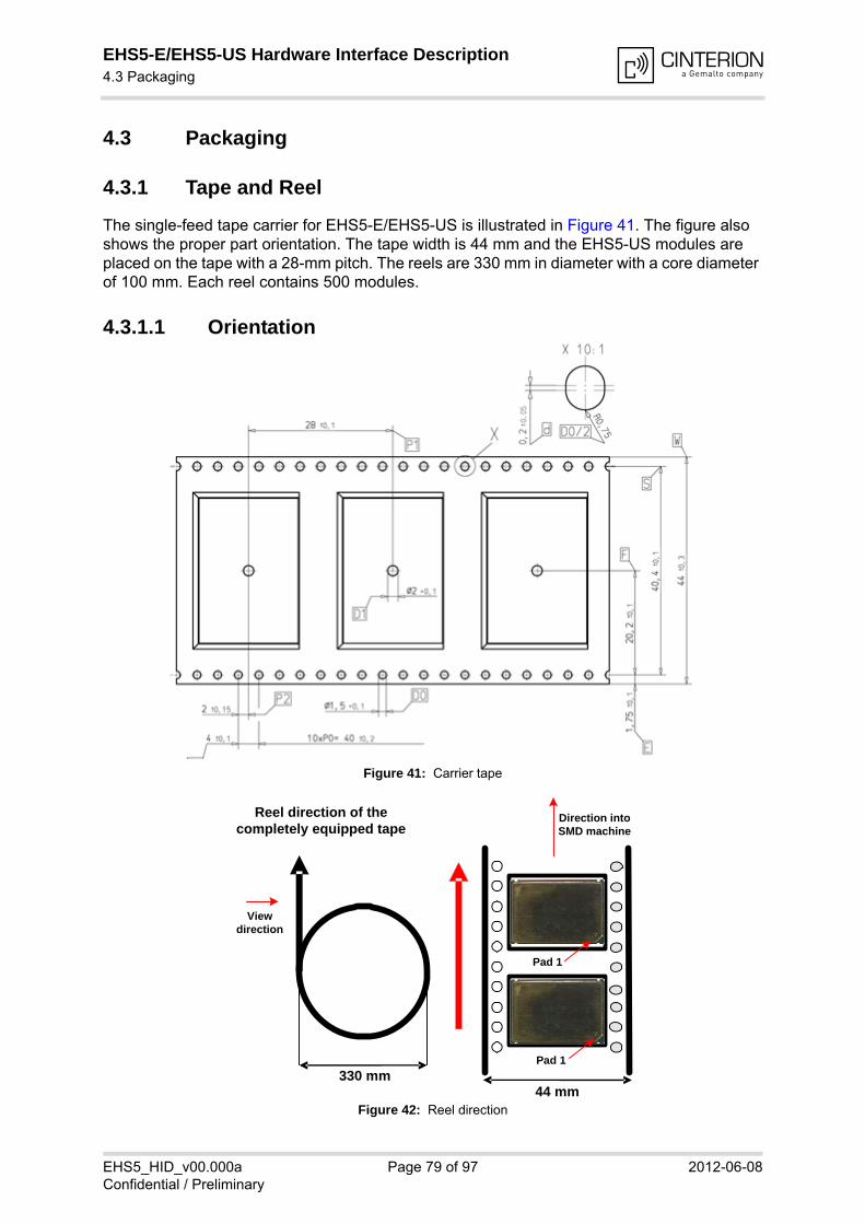
EHS5-E/EHS5-US Hardware Interface Description4.3 Packaging84
EHS5_HID_v00.000a Page 79 of 97 2012-06-08Confidential / Preliminary
4.3 Packaging
4.3.1 Tape and Reel
The single-feed tape carrier for EHS5-E/EHS5-US is illustrated in Figure 41. The figure also shows the proper part orientation. The tape width is 44 mm and the EHS5-US modules are placed on the tape with a 28-mm pitch. The reels are 330 mm in diameter with a core diameter of 100 mm. Each reel contains 500 modules.
4.3.1.1 Orientation
Figure 41: Carrier tape
Figure 42: Reel direction
44 mm 330 mm
Reel direction of the completely equipped tape
Direction into SMD machine
View direction
Pad 1
Pad 1

EHS5-E/EHS5-US Hardware Interface Description4.3 Packaging84
EHS5_HID_v00.000a Page 80 of 97 2012-06-08Confidential / Preliminary
4.3.1.2 Barcode Label
A barcode label provides detailed information on the tape and its contents. It is attached to the reel.
Figure 43: Barcode label on tape reel
Barcode label

EHS5-E/EHS5-US Hardware Interface Description4.3 Packaging84
EHS5_HID_v00.000a Page 81 of 97 2012-06-08Confidential / Preliminary
4.3.2 Shipping Materials
EHS5-E/EHS5-US is distributed in tape and reel carriers. The tape and reel carriers used to distribute EHS5-E/EHS5-US are packed as described below, including the following required shipping materials:• Moisture barrier bag, including desiccant and humidity indicator card• Transportation box
4.3.2.1 Moisture Barrier Bag
The tape reels are stored inside an MBB (=moisture barrier bag), together with a humidity indi-cator card and desiccant pouches - see Figure 44. The bag is ESD protected and delimits mois-ture transmission. It is vacuum-sealed and should be handled carefully to avoid puncturing or tearing. The bag protects the EHS5-E/EHS5-US modules from moisture exposure. It should not be opened until the devices are ready to be soldered onto the application.
Figure 44: Moisture barrier bag (MBB) with imprint
The label shown in Figure 45 summarizes requirements regarding moisture sensitivity, includ-ing shelf life and baking requirements. It is attached to the outside of the moisture barrier bag.

EHS5-E/EHS5-US Hardware Interface Description4.3 Packaging84
EHS5_HID_v00.000a Page 82 of 97 2012-06-08Confidential / Preliminary
Figure 45: Moisture Sensitivity Label

EHS5-E/EHS5-US Hardware Interface Description4.3 Packaging84
EHS5_HID_v00.000a Page 83 of 97 2012-06-08Confidential / Preliminary
MBBs contain one or more desiccant pouches to absorb moisture that may be in the bag. The humidity indicator card described below should be used to determine whether the enclosed components have absorbed an excessive amount of moisture.
The desiccant pouches should not be baked or reused once removed from the MBB.
The humidity indicator card is a moisture indicator and is included in the MBB to show the ap-proximate relative humidity level within the bag. Sample humidity cards are shown in Figure 46. If the components have been exposed to moisture above the recommended limits, the units will have to be rebaked.
Figure 46: Humidity Indicator Card - HIC
A baking is required if the humidity indicator inside the bag indicates 10% RH or more.
4.3.2.2 Transportation Box
Tape and reel carriers are distributed in a box, marked with a barcode label for identification purposes. A box contains two reels with 500 modules each.

EHS5-E/EHS5-US Hardware Interface Description4.3 Packaging84
EHS5_HID_v00.000a Page 84 of 97 2012-06-08Confidential / Preliminary
4.3.3 Trays
If small module quantities are required, e.g., for test and evaluation purposes, EHS5-E/EHS5-US may be distrib-uted in trays. The small quantity trays are an alternative to the single-feed tape carriers normally used. However, the trays are not designed for machine processing. They contain modules to be (hand) soldered onto an external application (for information on hand soldering see [3]).
Figure 47: Small quantity tray
Trays are packed and shipped in the same way as tape carriers, including a moisture barrier bag with desiccant and humidity indicator card as well as a transportation box (see also Section 4.3.2).
Figure 48: Tray to ship odd module amounts
Figure 49: Trays with packaging materials
1:1,5

EHS5-E/EHS5-US Hardware Interface Description5 Regulatory and Type Approval Information90
EHS5_HID_v00.000a Page 85 of 97 2012-06-08Confidential / Preliminary
5 Regulatory and Type Approval Information
5.1 Directives and Standards
EHS5-E/EHS5-US is designed to comply with the directives and standards listed below.
It is the responsibility of the application manufacturer to ensure compliance of the final product with all provisions of the applicable directives and standards as well as with the technical spec-ifications provided in the "EHS5-E/EHS5-US Hardware Interface Description".1
1. Manufacturers of applications which can be used in the US shall ensure that their applications have aPTCRB approval. For this purpose they can refer to the PTCRB approval of the respective module.
Table 19: Directives
1999/05/EC Directive of the European Parliament and of the council of 9 March 1999 on radio equipment and telecommunications terminal equipment and the mutual recognition of their conformity (in short referred to as R&TTE Direc-tive 1999/5/EC).The product is labeled with the CE conformity mark
2002/95/EC Directive of the European Parliament and of the Council of 27 January 2003 on the restriction of the use of certain hazardous substances in electrical and electronic equip-ment (RoHS)
Table 20: Standards of North American type approval1
1. Applies to the module variant EHS5-US only.
CFR Title 47 Code of Federal Regulations, Part 22 and Part 24 (Telecommunications, PCS); US Equipment Authorization FCC
OET Bulletin 65 (Edition 97-01)
Evaluating Compliance with FCC Guidelines for Human Exposure to Radiofrequency Electromagnetic Fields
UL 60 950-1 Product Safety Certification (Safety requirements)
NAPRD.03 V5.12 Overview of PCS Type certification review board Mobile Equipment Type Certification and IMEI controlPCS Type Certification Review board (PTCRB)
RSS132 (Issue2)RSS133 (Issue5)
Canadian Standard
Table 21: Standards of European type approval1
3GPP TS 51.010-1 Digital cellular telecommunications system (Release 7); Mobile Station (MS) conformance specification;
ETSI EN 301 511 V9.0.2 Global System for Mobile communications (GSM); Harmonized standard for mobile stations in the GSM 900 and DCS 1800 bands covering essential requirements under article 3.2 of the R&TTE directive (1999/5/EC)
GCF-CC V3.46 Global Certification Forum - Certification Criteria

EHS5-E/EHS5-US Hardware Interface Description5.1 Directives and Standards90
EHS5_HID_v00.000a Page 86 of 97 2012-06-08Confidential / Preliminary
ETSI EN 301 489-01 V1.8.1
Electromagnetic Compatibility and Radio spectrum Matters (ERM); Electro-magnetic Compatibility (EMC) standard for radio equipment and services; Part 1: Common Technical Requirements
ETSI EN 301 489-03 V1.4.1
Electromagnetic Compatibility and Radio spectrum Matters (ERM); Electro-magnetic Compatibility (EMC) standard for radio equipment and services; Part 3: Specific conditions for Short-Range Devices (SRD) operating on fre-quencies between 9 kHz and 40 GHz
ETSI EN 301 489-07 V1.3.1
Electromagnetic Compatibility and Radio spectrum Matters (ERM); Electro-magnetic Compatibility (EMC) standard for radio equipment and services; Part 7: Specific conditions for mobile and portable radio and ancillary equip-ment of digital cellular radio telecommunications systems (GSM and DCS)
ETSI EN 301 489-24 V1.5.1
Electromagnetic Compatibility and Radio spectrum Matters (ERM); Electro-magnetic Compatibility (EMC) standard for radio equipment and services; Part 24: Specific conditions for IMT-2000 CDMA Direct Spread (UTRA) for Mobile and portable (UE) radio and ancillary equipment
ETSI EN 301 908-01 V4.2.1
Electromagnetic compatibility and Radio spectrum Matters (ERM); Base Stations (BS) and User Equipment (UE) for IMT-2000 Third Generation cel-lular networks; Part 1: Harmonized EN for IMT-2000, introduction and com-mon requirements of article 3.2 of the R&TTE Directive
ETSI EN 301 908-02 V4.2.1
Electromagnetic compatibility and Radio spectrum Matters (ERM); Base Stations (BS) and User Equipment (UE) for IMT-2000 Third Generation cel-lular networks; Part 2: Harmonized EN for IMT-2000, CDMA Direct Spread (UTRA FDD) (UE) covering essential requirements of article 3.2 of the R&TTE Directive
ETSI EN 300 440-02 V1.4.1
Electromagnetic compatibility and Radio spectrum Matters (ERM); Short range devices; Radio equipment to be used in the 1 GHz to 40 GHz fre-quency range; Part 2: Harmonized EN covering essential requirements of article 3.2 of the R&TTE Directive
EN 62311:2008 Assessment of electronic and electrical equipment related to human expo-sure restrictions for electromagnetic fields (0 Hz - 300 GHz)
IEC/EN 60950-1:2006/A1:2010IEC 60950-1:2005/A1:2009(second edition)
Safety of information technology equipment
1. Applies to the module variant EHS5-E only.
Table 22: Requirements of quality
IEC 60068 Environmental testing
DIN EN 60529 IP codes
Table 23: Standards of the Ministry of Information Industry of the People’s Republic of China
SJ/T 11363-2006 “Requirements for Concentration Limits for Certain Hazardous Sub-stances in Electronic Information Products” (2006-06).
Table 21: Standards of European type approval1
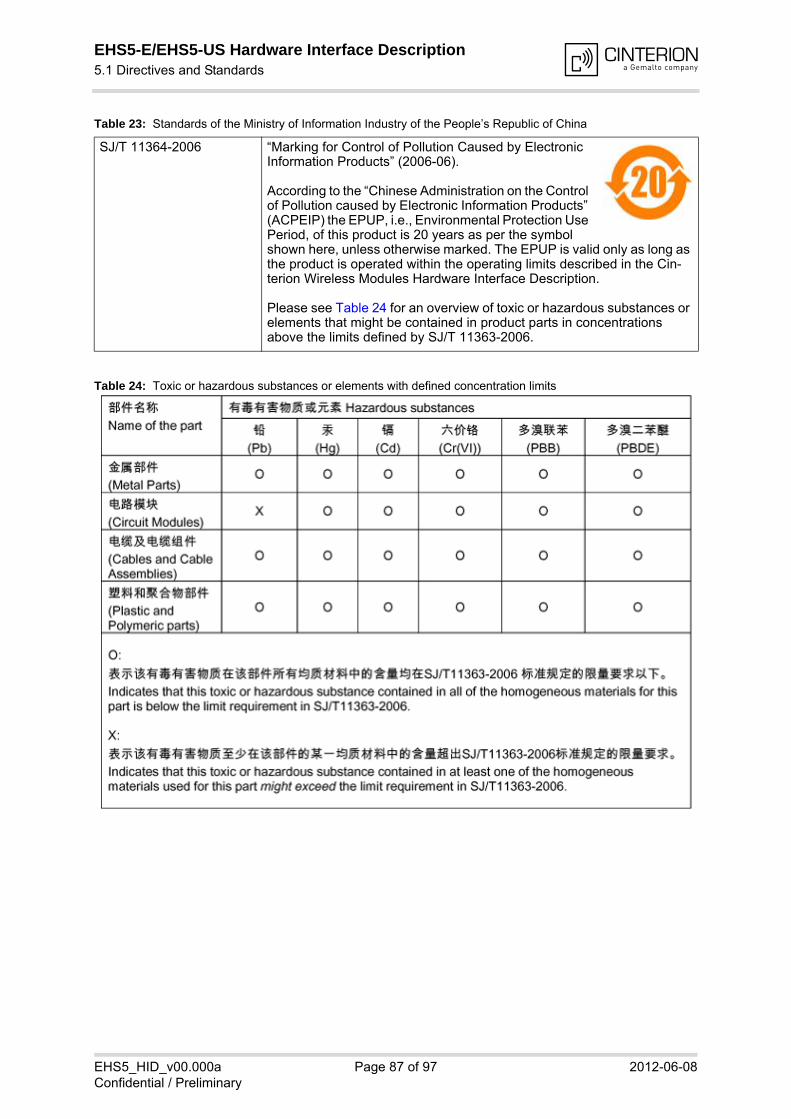
EHS5-E/EHS5-US Hardware Interface Description5.1 Directives and Standards90
EHS5_HID_v00.000a Page 87 of 97 2012-06-08Confidential / Preliminary
Table 24: Toxic or hazardous substances or elements with defined concentration limits
SJ/T 11364-2006 “Marking for Control of Pollution Caused by Electronic Information Products” (2006-06).
According to the “Chinese Administration on the Control of Pollution caused by Electronic Information Products” (ACPEIP) the EPUP, i.e., Environmental Protection Use Period, of this product is 20 years as per the symbol shown here, unless otherwise marked. The EPUP is valid only as long as the product is operated within the operating limits described in the Cin-terion Wireless Modules Hardware Interface Description.
Please see Table 24 for an overview of toxic or hazardous substances or elements that might be contained in product parts in concentrations above the limits defined by SJ/T 11363-2006.
Table 23: Standards of the Ministry of Information Industry of the People’s Republic of China

EHS5-E/EHS5-US Hardware Interface Description5.2 SAR requirements specific to portable mobiles90
EHS5_HID_v00.000a Page 88 of 97 2012-06-08Confidential / Preliminary
5.2 SAR requirements specific to portable mobiles
Mobile phones, PDAs or other portable transmitters and receivers incorporating a GSM module must be in accordance with the guidelines for human exposure to radio frequency energy. This requires the Specific Absorption Rate (SAR) of portable EHS5-E/EHS5-US based applications to be evaluated and approved for compliance with national and/or international regulations.
Since the SAR value varies significantly with the individual product design manufacturers are advised to submit their product for approval if designed for portable use. For European and US markets the relevant directives are mentioned below. It is the responsibility of the manufacturer of the final product to verify whether or not further standards, recommendations or directives are in force outside these areas.
Products intended for sale on US markets1
ES 59005/ANSI C95.1 Considerations for evaluation of human exposure to Electromagnetic Fields (EMFs) from Mobile Telecommunication Equipment (MTE) in thefrequency range 30MHz - 6GHz
Products intended for sale on European markets
EN 50360 Product standard to demonstrate the compliance of mobile phones withthe basic restrictions related to human exposure to electromagnetic fields (300MHz - 3GHz)
1. Applies for the quad band module variant EHS5-US only.

EHS5-E/EHS5-US Hardware Interface Description5.3 Reference Equipment for Type Approval90
EHS5_HID_v00.000a Page 89 of 97 2012-06-08Confidential / Preliminary
5.3 Reference Equipment for Type Approval
The Cinterion Wireless Modules reference setup submitted to type approve EHS5-E/EHS5-US (including a special approval adapter for the DSB75) is shown in the following figure:
Figure 50: Reference equipment for Type Approval
Antenna
GSM / GPRS / UMTS Antenna with 1m cable
ASC0PC
Power supply
GSM / GPRS / UMTSBase station
DSB75
Audio test system
Handset
ASC1
USB
Codec adapter
DAI
Analog Audio
Approval adapter for DSB75
SMA
Evaluation module
EHS5
USB
Evaluation module
EHS5
SIM card
Audio

EHS5-E/EHS5-US Hardware Interface Description5.4 Compliance with FCC and IC Rules and Regulations90
EHS5_HID_v00.000a Page 90 of 97 2012-06-08Confidential / Preliminary
5.4 Compliance with FCC and IC Rules and Regulations
The Equipment Authorization Certification for the Cinterion Wireless Modules reference appli-cation described in Section 5.3 will be registered under the following identifiers1:
FCC Identifier: QIPEHS5Industry Canada Certification Number: 7830A-EHS5Granted to Cinterion Wireless Modules GmbH
Manufacturers of mobile or fixed devices incorporating EHS5-US modules are authorized to use the FCC Grants and Industry Canada Certificates of the EHS5-US modules for their own final products according to the conditions referenced in these documents. In this case, an FCC/ IC label of the module shall be visible from the outside, or the host device shall bear a second label stating "Contains FCC ID QIPEHS5", and accordingly “Contains IC 7830A-EHS5“.
IMPORTANT: Manufacturers of portable applications incorporating EHS5-US modules are required to have their final product certified and apply for their own FCC Grant and Industry Canada Certificate related to the specific portable mobile. This is mandatory to meet the SAR requirements for por-table mobiles (see Section 5.2 for detail).
Changes or modifications not expressly approved by the party responsible for compliance could void the user's authority to operate the equipment.
1. Applies only for the quad band module variant EHS5-US.

EHS5-E/EHS5-US Hardware Interface Description6 Document Information95
EHS5_HID_v00.000a Page 91 of 97 2012-06-08Confidential / Preliminary
6 Document Information
6.1 Revision History
Preceding document: "EHS5-E/EHS5-US Hardware Interface Description" Version 00.000New document: "EHS5-E/EHS5-US Hardware Interface Description" Version 00.000a
New document: "EHS5-E/EHS5-US Hardware Interface Description" Version 00.000
6.2 Related Documents
[1] EHS5-E/EHS5-US AT Command Set[2] EHS5-E/EHS5-US Release Note[3] Application Note 48: SMT Module Integration
6.3 Terms and Abbreviations
Chapter What is new
2.1.1 Slightly revised color scheme in Figure 3. Pads 104, 105, 106 are assigned to GND.
2.1.3 Added internal serial resistor (RS) to Figure 4.
2.1.12.5 New section Fast Shutdown.
3.2.1.1 Revised Figure 27 illustrating an ON circuit sample (value for R2).
7.1 Added ordering information for Multi-Adapter R1 and Approval adapter.
Chapter What is new
-- Initial document setup.
Abbreviation Description
ADC Analog-to-digital converter
AGC Automatic Gain Control
ANSI American National Standards Institute
ARFCN Absolute Radio Frequency Channel Number
ARP Antenna Reference Point
ASC0/ASC1 Asynchronous Controller. Abbreviations used for first and second serial interface of EHS5-E/EHS5-US
B Thermistor Constant
BER Bit Error Rate
BTS Base Transceiver Station

EHS5-E/EHS5-US Hardware Interface Description6.3 Terms and Abbreviations95
EHS5_HID_v00.000a Page 92 of 97 2012-06-08Confidential / Preliminary
CB or CBM Cell Broadcast Message
CE Conformité Européene (European Conformity)
CHAP Challenge Handshake Authentication Protocol
CPU Central Processing Unit
CS Coding Scheme
CSD Circuit Switched Data
CTS Clear to Send
DAC Digital-to-Analog Converter
DAI Digital Audio Interface
dBm0 Digital level, 3.14dBm0 corresponds to full scale, see ITU G.711, A-law
DCE Data Communication Equipment (typically modems, e.g. Cinterion GSM module)
DCS 1800 Digital Cellular System, also referred to as PCN
DRX Discontinuous Reception
DSB Development Support Box
DSP Digital Signal Processor
DSR Data Set Ready
DTE Data Terminal Equipment (typically computer, terminal, printer or, for example, GSM application)
DTR Data Terminal Ready
DTX Discontinuous Transmission
EFR Enhanced Full Rate
EGSM Enhanced GSM
EIRP Equivalent Isotropic Radiated Power
EMC Electromagnetic Compatibility
ERP Effective Radiated Power
ESD Electrostatic Discharge
ETS European Telecommunication Standard
FCC Federal Communications Commission (U.S.)
FDMA Frequency Division Multiple Access
FR Full Rate
GMSK Gaussian Minimum Shift Keying
GPIO General Purpose Input/Output
GPRS General Packet Radio Service
GSM Global Standard for Mobile Communications
HiZ High Impedance
HR Half Rate
I/O Input/Output
IC Integrated Circuit
Abbreviation Description

EHS5-E/EHS5-US Hardware Interface Description6.3 Terms and Abbreviations95
EHS5_HID_v00.000a Page 93 of 97 2012-06-08Confidential / Preliminary
IMEI International Mobile Equipment Identity
ISO International Standards Organization
ITU International Telecommunications Union
kbps kbits per second
LED Light Emitting Diode
Li-Ion/Li+ Lithium-Ion
Li battery Rechargeable Lithium Ion or Lithium Polymer battery
Mbps Mbits per second
MMI Man Machine Interface
MO Mobile Originated
MS Mobile Station (GSM module), also referred to as TE
MSISDN Mobile Station International ISDN number
MT Mobile Terminated
NTC Negative Temperature Coefficient
OEM Original Equipment Manufacturer
PA Power Amplifier
PAP Password Authentication Protocol
PBCCH Packet Switched Broadcast Control Channel
PCB Printed Circuit Board
PCL Power Control Level
PCM Pulse Code Modulation
PCN Personal Communications Network, also referred to as DCS 1800
PCS Personal Communication System, also referred to as GSM 1900
PDU Protocol Data Unit
PLL Phase Locked Loop
PPP Point-to-point protocol
PSK Phase Shift Keying
PSU Power Supply Unit
PWM Pulse Width Modulation
R&TTE Radio and Telecommunication Terminal Equipment
RAM Random Access Memory
RF Radio Frequency
RLS Radio Link Stability
RMS Root Mean Square (value)
RoHS Restriction of the use of certain hazardous substances in electrical and electronic equipment.
ROM Read-only Memory
RTC Real Time Clock
Abbreviation Description

EHS5-E/EHS5-US Hardware Interface Description6.3 Terms and Abbreviations95
EHS5_HID_v00.000a Page 94 of 97 2012-06-08Confidential / Preliminary
RTS Request to Send
Rx Receive Direction
SAR Specific Absorption Rate
SAW Surface Accoustic Wave
SELV Safety Extra Low Voltage
SIM Subscriber Identification Module
SMD Surface Mount Device
SMS Short Message Service
SMT Surface Mount Technology
SRAM Static Random Access Memory
TA Terminal adapter (e.g. GSM module)
TDMA Time Division Multiple Access
TE Terminal Equipment, also referred to as DTE
TLS Transport Layer Security
Tx Transmit Direction
UART Universal asynchronous receiver-transmitter
URC Unsolicited Result Code
USSD Unstructured Supplementary Service Data
VSWR Voltage Standing Wave Ratio
Abbreviation Description

EHS5-E/EHS5-US Hardware Interface Description6.4 Safety Precaution Notes95
EHS5_HID_v00.000a Page 95 of 97 2012-06-08Confidential / Preliminary
6.4 Safety Precaution Notes
The following safety precautions must be observed during all phases of the operation, usage, service or repair of any cellular terminal or mobile incorporating EHS5-E/EHS5-US. Manufac-turers of the cellular terminal are advised to convey the following safety information to users and operating personnel and to incorporate these guidelines into all manuals supplied with the product. Failure to comply with these precautions violates safety standards of design, manu-facture and intended use of the product. Cinterion Wireless Modules assumes no liability for customer’s failure to comply with these precautions.
When in a hospital or other health care facility, observe the restrictions on the use of mobiles. Switch the cellular terminal or mobile off, if instructed to do so by the guide-lines posted in sensitive areas. Medical equipment may be sensitive to RF energy. The operation of cardiac pacemakers, other implanted medical equipment and hear-ing aids can be affected by interference from cellular terminals or mobiles placed close to the device. If in doubt about potential danger, contact the physician or the manufac-turer of the device to verify that the equipment is properly shielded. Pacemaker patients are advised to keep their hand-held mobile away from the pacemaker, while it is on.
Switch off the cellular terminal or mobile before boarding an aircraft. Make sure it can-not be switched on inadvertently. The operation of wireless appliances in an aircraft is forbidden to prevent interference with communications systems. Failure to observe these instructions may lead to the suspension or denial of cellular services to the offender, legal action, or both.
Do not operate the cellular terminal or mobile in the presence of flammable gases or fumes. Switch off the cellular terminal when you are near petrol stations, fuel depots, chemical plants or where blasting operations are in progress. Operation of any elec-trical equipment in potentially explosive atmospheres can constitute a safety hazard.
Your cellular terminal or mobile receives and transmits radio frequency energy while switched on. Remember that interference can occur if it is used close to TV sets, radios, computers or inadequately shielded equipment. Follow any special regulations and always switch off the cellular terminal or mobile wherever forbidden, or when you suspect that it may cause interference or danger.
Road safety comes first! Do not use a hand-held cellular terminal or mobile when driv-ing a vehicle, unless it is securely mounted in a holder for speakerphone operation. Before making a call with a hand-held terminal or mobile, park the vehicle. Speakerphones must be installed by qualified personnel. Faulty installation or opera-tion can constitute a safety hazard.
IMPORTANT!Cellular terminals or mobiles operate using radio signals and cellular networks. Because of this, connection cannot be guaranteed at all times under all conditions. Therefore, you should never rely solely upon any wireless device for essential com-munications, for example emergency calls. Remember, in order to make or receive calls, the cellular terminal or mobile must be switched on and in a service area with adequate cellular signal strength. Some networks do not allow for emergency calls if certain network services or phone features are in use (e.g. lock functions, fixed dialing etc.). You may need to deactivate those features before you can make an emergency call.Some networks require that a valid SIM card be properly inserted in the cellular termi-nal or mobile.
EHS5-E/EHS5-US Hardware Interface Description7 Appendix97
EHS5_HID_v00.000a Page 96 of 97 2012-06-08Confidential / Preliminary
7 Appendix
7.1 List of Parts and Accessories
Table 25: List of parts and accessories
Description Supplier Ordering information
EHS5-E/EHS5-US Cinterion Standard module Cinterion Wireless Modules IMEI:Ordering number: L30960-N2800-A100 (EHS5-E)Ordering number: L30960-N2810-A100 (EHS5-US)
Customer IMEI mode:Ordering number: L30960-N2805-A100 (EHS5-E)Ordering number: L30960-N2815-A100 (EHS5-US)
DSB75 Evaluation Kit Cinterion Ordering number: L36880-N8811-A100
Multi-Adapter R1 for mount-ing EHS5-E/EHS5-US evalu-ation modules onto DSB75
Cinterion Ordering number: L30960-N0010-A100
Approval adapter for mount-ing EHS5-E/EHS5-US evalu-ation modules onto DSB75
Cinterion Ordering number: L30960-N2301-A100
Evaluation Module Cinterion Ordering number: L30960-N2801-A100 (EHS5-E)Ordering number: L30960-N2811-A100 (EHS5-US)
Votronic Handset VOTRONIC / Cinterion
Cinterion ordering number: L36880-N8301-A107Votronic ordering number: HH-SI-30.3/V1.1/0VOTRONIC Entwicklungs- und Produktionsgesellschaft für elek-tronische Geräte mbHSaarbrücker Str. 866386 St. IngbertGermanyPhone: +49-(0)6 89 4 / 92 55-0Fax: +49-(0)6 89 4 / 92 55-88Email: [email protected]
SIM card holder incl. push button ejector and slide-in tray
Molex Ordering numbers: 91228 91236
Sales contacts are listed in Table 26.

EHS5-E/EHS5-US Hardware Interface Description7.1 List of Parts and Accessories97
EHS5_HID_v00.000a Page 97 of 97 2012-06-08Confidential / Preliminary
Table 26: Molex sales contacts (subject to change)
MolexFor further information please click:http://www.molex.com
Molex Deutschland GmbHOtto-Hahn-Str. 1b69190 WalldorfGermanyPhone: +49-6227-3091-0Fax: +49-6227-3091-8100Email: [email protected]
American HeadquartersLisle, Illinois 60532U.S.A.Phone: +1-800-78MOLEXFax: +1-630-969-1352
Molex China DistributorsBeijing, Room 1311, Tower B, COFCO PlazaNo. 8, Jian Guo Men Nei Street, 100005BeijingP.R. ChinaPhone: +86-10-6526-9628 Fax: +86-10-6526-9730
Molex Singapore Pte. Ltd.110, International RoadJurong Town, Singapore 629174
Phone: +65-6-268-6868Fax: +65-6-265-6044
Molex Japan Co. Ltd.1-5-4 Fukami-Higashi,Yamato-City,Kanagawa, 242-8585 Japan
Phone: +81-46-265-2325Fax: +81-46-265-2365