Embed Size (px)
Citation preview
HardwareDocumentation
Linear Hall-Effect Sensor Family
HAL® 83x
Robust Multi-Purpose Programmable
Edition May 22, 2015DSH000169_002EN
Data Sheet
HAL 83x DATA SHEET
2 May 22, 2015; DSH000169_002E Micronas
Copyright, Warranty, and Limitation of Liability
The information and data contained in this documentare believed to be accurate and reliable. The softwareand proprietary information contained therein may beprotected by copyright, patent, trademark and/or otherintellectual property rights of Micronas. All rights notexpressly granted remain reserved by Micronas.
Micronas assumes no liability for errors and gives nowarranty representation or guarantee regarding thesuitability of its products for any particular purpose dueto these specifications.
By this publication, Micronas does not assume respon-sibility for patent infringements or other rights of thirdparties which may result from its use. Commercial con-ditions, product availability and delivery are exclusivelysubject to the respective order confirmation.
Any information and data which may be provided in thedocument can and do vary in different applications,and actual performance may vary over time.
All operating parameters must be validated for eachcustomer application by customers’ technical experts.Any new issue of this document invalidates previousissues. Micronas reserves the right to review this docu-ment and to make changes to the document’s contentat any time without obligation to notify any person orentity of such revision or changes. For further adviceplease contact us directly.
Do not use our products in life-supporting systems,military, aviation, or aerospace applications! Unlessexplicitly agreed to otherwise in writing between theparties, Micronas’ products are not designed, intendedor authorized for use as components in systemsintended for surgical implants into the body, or otherapplications intended to support or sustain life, or forany other application in which the failure of the productcould create a situation where personal injury or deathcould occur.
No part of this publication may be reproduced, photo-copied, stored on a retrieval system or transmittedwithout the express written consent of Micronas.
Micronas Trademarks
– HAL
Micronas Patents
EP0 953 848, EP 1 039 357, EP 1 575 013
Third-Party Trademarks
All other brand and product names or company namesmay be trademarks of their respective companies.
3 May 22, 2015; DSH000169_002E Micronas
Contents
Page Section Title
HAL 83x DATA SHEET
4 1. Introduction4 1.1. Applications4 1.2. General Features4 1.2.1. Device-specific features of HAL835
5 2. Ordering Information5 2.1. Device-Specific Ordering Codes
6 3. Functional Description6 3.1. General Function8 3.2. Digital Signal Processing and EEPROM12 3.3. Calibration Procedure12 3.3.1. General Procedure
14 4. Specifications14 4.1. Outline Dimensions18 4.2. Soldering, Welding and Assembly18 4.3. Pin Connections and Short Descriptions18 4.4. Dimensions of Sensitive Area18 4.5. Physical Dimensions19 4.6. Absolute Maximum Ratings20 4.6.1. Storage and Shelf Life20 4.7. Recommended Operating Conditions21 4.8. Characteristics23 4.8.1. Definition of sensitivity error ES24 4.8.2. Power-On Operation25 4.9. Diagnostics and Safety Features25 4.9.1. Overvoltage and Undervoltage Detection25 4.9.2. Open-Circuit Detection25 4.9.3. Overtemperature and Short-Circuit Protection25 4.9.4. EEPROM Redundancy25 4.9.5. ADC Diagnostic
26 5. Application Notes26 5.1. Application Circuit (for analog output mode only)26 5.2. Use of two HAL83x in Parallel
(for analog output mode only)27 5.3. Temperature Compensation28 5.4. Ambient Temperature28 5.5. EMC and ESD
29 6. Programming29 6.1. Definition of Programming Pulses29 6.2. Definition of the Telegram31 6.3. Telegram Codes32 6.4. Number Formats32 6.5. Register Information34 6.6. Programming Information
35 7. Data Sheet History
HAL 83x DATA SHEET
4 May 22, 2015; DSH000169_002E Micronas
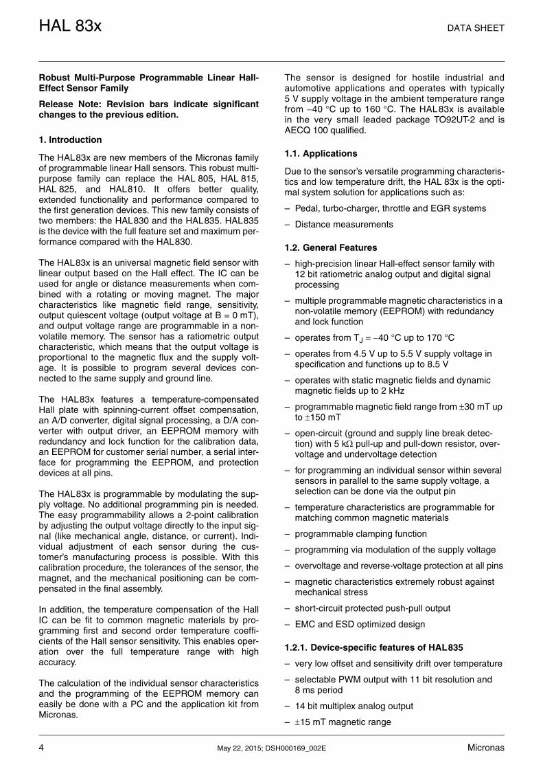
Robust Multi-Purpose Programmable Linear Hall-Effect Sensor Family
Release Note: Revision bars indicate significantchanges to the previous edition.
1. Introduction
The HAL83x are new members of the Micronas familyof programmable linear Hall sensors. This robust multi-purpose family can replace the HAL 805, HAL 815,HAL 825, and HAL810. It offers better quality,extended functionality and performance compared tothe first generation devices. This new family consists oftwo members: the HAL830 and the HAL835. HAL835is the device with the full feature set and maximum per-formance compared with the HAL830.
The HAL83x is an universal magnetic field sensor withlinear output based on the Hall effect. The IC can beused for angle or distance measurements when com-bined with a rotating or moving magnet. The majorcharacteristics like magnetic field range, sensitivity,output quiescent voltage (output voltage at B = 0 mT),and output voltage range are programmable in a non-volatile memory. The sensor has a ratiometric outputcharacteristic, which means that the output voltage isproportional to the magnetic flux and the supply volt-age. It is possible to program several devices con-nected to the same supply and ground line.
The HAL83x features a temperature-compensatedHall plate with spinning-current offset compensation,an A/D converter, digital signal processing, a D/A con-verter with output driver, an EEPROM memory withredundancy and lock function for the calibration data,an EEPROM for customer serial number, a serial inter-face for programming the EEPROM, and protectiondevices at all pins.
The HAL83x is programmable by modulating the sup-ply voltage. No additional programming pin is needed.The easy programmability allows a 2-point calibrationby adjusting the output voltage directly to the input sig-nal (like mechanical angle, distance, or current). Indi-vidual adjustment of each sensor during the cus-tomer’s manufacturing process is possible. With thiscalibration procedure, the tolerances of the sensor, themagnet, and the mechanical positioning can be com-pensated in the final assembly.
In addition, the temperature compensation of the HallIC can be fit to common magnetic materials by pro-gramming first and second order temperature coeffi-cients of the Hall sensor sensitivity. This enables oper-ation over the full temperature range with highaccuracy.
The calculation of the individual sensor characteristicsand the programming of the EEPROM memory caneasily be done with a PC and the application kit fromMicronas.
The sensor is designed for hostile industrial andautomotive applications and operates with typically5 V supply voltage in the ambient temperature rangefrom 40 °C up to 160 °C. The HAL83x is availablein the very small leaded package TO92UT-2 and isAECQ 100 qualified.
1.1. Applications
Due to the sensor’s versatile programming characteris-tics and low temperature drift, the HAL 83x is the opti-mal system solution for applications such as:
– Pedal, turbo-charger, throttle and EGR systems
– Distance measurements
1.2. General Features
– high-precision linear Hall-effect sensor family with 12 bit ratiometric analog output and digital signal processing
– multiple programmable magnetic characteristics in a non-volatile memory (EEPROM) with redundancy and lock function
– operates from TJ = 40 °C up to 170 °C
– operates from 4.5 V up to 5.5 V supply voltage in specification and functions up to 8.5 V
– operates with static magnetic fields and dynamic magnetic fields up to 2 kHz
– programmable magnetic field range from 30 mT up to 150 mT
– open-circuit (ground and supply line break detec-tion) with 5 k pull-up and pull-down resistor, over-voltage and undervoltage detection
– for programming an individual sensor within several sensors in parallel to the same supply voltage, a selection can be done via the output pin
– temperature characteristics are programmable for matching common magnetic materials
– programmable clamping function
– programming via modulation of the supply voltage
– overvoltage and reverse-voltage protection at all pins
– magnetic characteristics extremely robust against mechanical stress
– short-circuit protected push-pull output
– EMC and ESD optimized design
1.2.1. Device-specific features of HAL835
– very low offset and sensitivity drift over temperature
– selectable PWM output with 11 bit resolution and 8 ms period
– 14 bit multiplex analog output
– 15 mT magnetic range
DATA SHEET HAL 83x
Micronas May 22, 2015; DSH000169_002E 5
2. Ordering Information
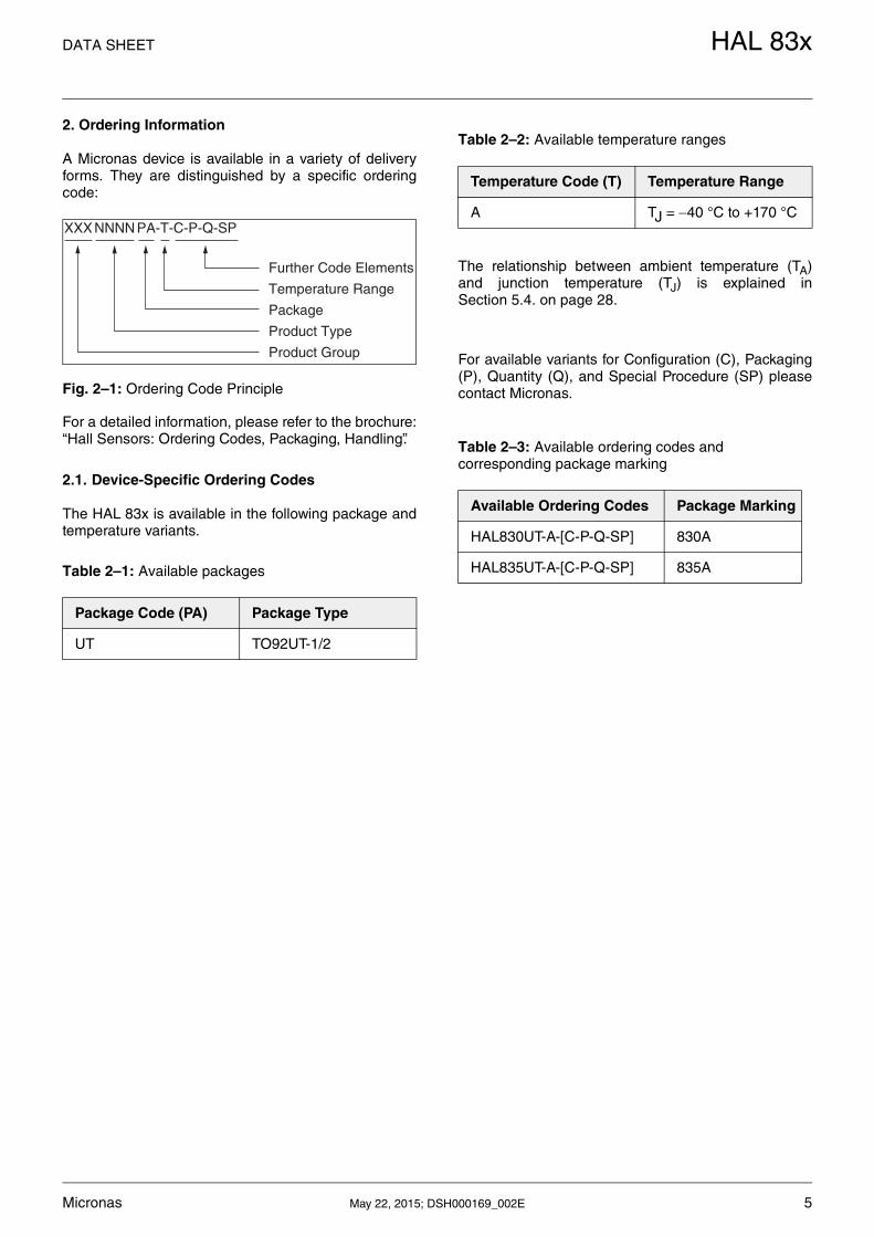
A Micronas device is available in a variety of deliveryforms. They are distinguished by a specific orderingcode:
Fig. 2–1: Ordering Code Principle
For a detailed information, please refer to the brochure:“Hall Sensors: Ordering Codes, Packaging, Handling”.
2.1. Device-Specific Ordering Codes
The HAL 83x is available in the following package andtemperature variants.
The relationship between ambient temperature (TA)and junction temperature (TJ) is explained inSection 5.4. on page 28.
For available variants for Configuration (C), Packaging(P), Quantity (Q), and Special Procedure (SP) pleasecontact Micronas.
Table 2–1: Available packages
Package Code (PA) Package Type
UT TO92UT-1/2
XXX NNNN PA-T-C-P-Q-SP
Further Code Elements
Temperature Range
Package
Product Type
Product Group
Table 2–2: Available temperature ranges
Temperature Code (T) Temperature Range
A TJ = 40 °C to +170 °C
Table 2–3: Available ordering codes and corresponding package marking
Available Ordering Codes Package Marking
HAL830UT-A-[C-P-Q-SP] 830A
HAL835UT-A-[C-P-Q-SP] 835A
HAL 83x DATA SHEET
6 May 22, 2015; DSH000169_002E Micronas
3. Functional Description
3.1. General Function
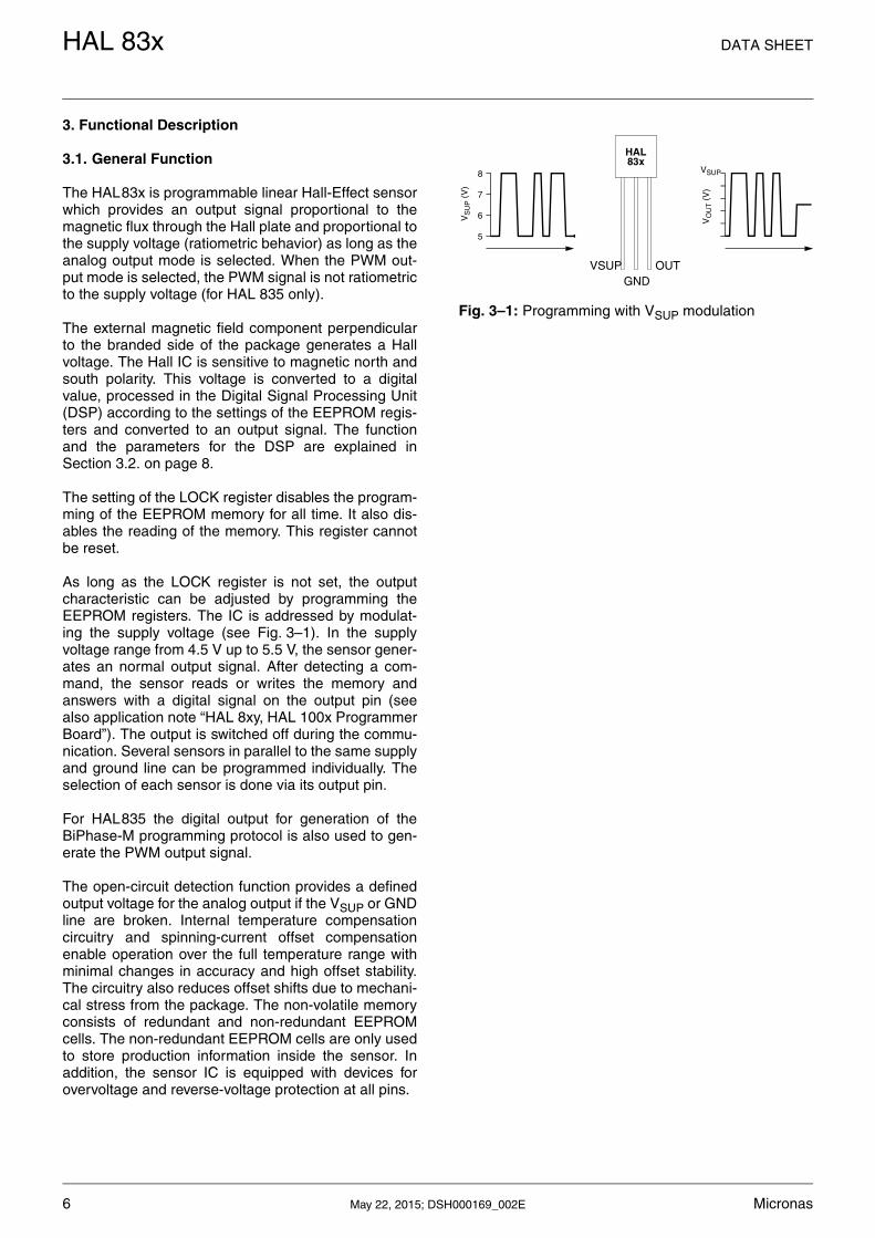
The HAL83x is programmable linear Hall-Effect sensorwhich provides an output signal proportional to themagnetic flux through the Hall plate and proportional tothe supply voltage (ratiometric behavior) as long as theanalog output mode is selected. When the PWM out-put mode is selected, the PWM signal is not ratiometricto the supply voltage (for HAL 835 only).
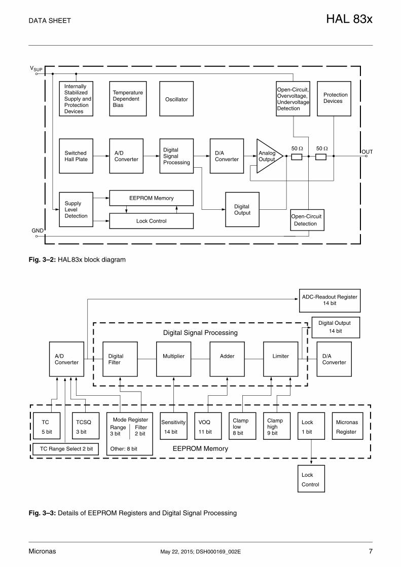
The external magnetic field component perpendicularto the branded side of the package generates a Hallvoltage. The Hall IC is sensitive to magnetic north andsouth polarity. This voltage is converted to a digitalvalue, processed in the Digital Signal Processing Unit(DSP) according to the settings of the EEPROM regis-ters and converted to an output signal. The functionand the parameters for the DSP are explained inSection 3.2. on page 8.
The setting of the LOCK register disables the program-ming of the EEPROM memory for all time. It also dis-ables the reading of the memory. This register cannotbe reset.
As long as the LOCK register is not set, the outputcharacteristic can be adjusted by programming theEEPROM registers. The IC is addressed by modulat-ing the supply voltage (see Fig. 3–1). In the supplyvoltage range from 4.5 V up to 5.5 V, the sensor gener-ates an normal output signal. After detecting a com-mand, the sensor reads or writes the memory andanswers with a digital signal on the output pin (seealso application note “HAL 8xy, HAL 100x ProgrammerBoard”). The output is switched off during the commu-nication. Several sensors in parallel to the same supplyand ground line can be programmed individually. Theselection of each sensor is done via its output pin.
For HAL835 the digital output for generation of theBiPhase-M programming protocol is also used to gen-erate the PWM output signal.
The open-circuit detection function provides a definedoutput voltage for the analog output if the VSUP or GNDline are broken. Internal temperature compensationcircuitry and spinning-current offset compensationenable operation over the full temperature range withminimal changes in accuracy and high offset stability.The circuitry also reduces offset shifts due to mechani-cal stress from the package. The non-volatile memoryconsists of redundant and non-redundant EEPROMcells. The non-redundant EEPROM cells are only usedto store production information inside the sensor. Inaddition, the sensor IC is equipped with devices forovervoltage and reverse-voltage protection at all pins.
Fig. 3–1: Programming with VSUP modulation
VO
UT (
V)
5
6
7
8
VS
UP (
V)
HAL83x
VSUPGND
OUT
VSUP
DATA SHEET HAL 83x
Micronas May 22, 2015; DSH000169_002E 7
Fig. 3–2: HAL83x block diagram
Fig. 3–3: Details of EEPROM Registers and Digital Signal Processing
InternallyTemperature
Oscillator
Switched50 Digital
D/A Analog
GND
SupplyEEPROM Memory
Lock Control
Digital
StabilizedSupply andProtectionDevices
DependentBias
ProtectionDevices
Hall PlateSignalProcessing
Converter Output
LevelDetection
Output
A/DConverter
Open-Circuit, Overvoltage,UndervoltageDetection
50
Open-CircuitDetection
OUT
VSUP
Mode RegisterFilter
TC
5 bit
TCSQ
3 bit
Sensitivity
14 bit
VOQ
11 bit
Clamp Lock
1 bit
Micronas
Register2 bitRange3 bit
Clamp
EEPROM Memory
A/DConverter
DigitalFilter
Multiplier Adder Limiter D/AConverter
Digital Signal Processing
ADC-Readout Register14 bit
Lock
Control
14 bit
Digital Output
TC Range Select 2 bit
low high
Other: 8 bit
9 bit8 bit
HAL 83x DATA SHEET
8 May 22, 2015; DSH000169_002E Micronas
3.2. Digital Signal Processing and EEPROM
The DSP performs signal conditioning and allowsadaption of the sensor to the customer application.The parameters for the DSP are stored in theEEPROM registers. The details are shown in Fig. 3–3.
Terminology:
SENSITIVITY: name of the register or register value
Sensitivity: name of the parameter
The EEPROM registers consist of four groups:
Group 1 contains the registers for the adaptation of thesensor to the magnetic system: MODE for selectingthe magnetic field range and filter frequency, TC,TCSQ and TC-Range for the temperature characteris-tics of the magnetic sensitivity.
Group 2 contains the registers for defining the outputcharacteristics: SENSITIVITY, VOQ, CLAMP-LOW(MIN-OUT), CLAMP-HIGH (MAX-OUT) and OUTPUTMODE. The output characteristic of the sensor isdefined by these parameters.
– The parameter VOQ (Output Quiescent Voltage) cor-responds to the output signal at B = 0 mT.
– The parameter Sensitivity defines the magnetic sen-sitivity:
– The output voltage can be calculated as:
The output voltage range can be clamped by settingthe registers CLAMP-LOW and CLAMP-HIGH in orderto enable failure detection (such as short-circuits toVSUP or GND and open connections).
Group 3 contains the general purpose register GP. TheGP Register can be used to store customer informa-tion, like a serial number after manufacturing. Micronaswill use this GP REGISTER to store informations like,Lot number, wafer number, x and y position of the dieon the wafer, etc. This information can be read by thecustomer and stored in it’s own data base or it can stayin the sensor as is.
Group 4 contains the Micronas registers and LOCK forthe locking of all registers. The MICRONAS registersare programmed and locked during production. Theseregisters are used for oscillator frequency trimming, A/D converter offset compensation, and several otherspecial settings.
An external magnetic field generates a Hall voltage onthe Hall plate. The ADC converts the amplified positiveor negative Hall voltage (operates with magnetic northand south poles at the branded side of the package) toa digital value. This value can be read by the A/D-READOUT register to ensure that the suitable con-verter modulation is achieved. The digital signal is fil-tered in the internal low-pass filter and manipulatedaccording to the settings stored in the EEPROM. Thedigital value after signal processing is readable in theD/A-READOUT register. Depending on the program-mable magnetic range of the Hall IC, the operatingrange of the A/D converter is from 15 mT...+15 mT upto 150 mT...+150 mT.
During further processing, the digital signal is multi-plied with the sensitivity factor, added to the quiescentoutput voltage level and limited according to the clamp-ing voltage levels. The result is converted to an analogsignal and stabilized by a push-pull output transistorstage.
The D/A-READOUT at any given magnetic fielddepends on the programmed magnetic field range, thelow-pass filter, TC values and CLAMP-LOW andCLAMP-HIGH. The D/A-READOUT range is min. 0and max. 16383.
Note: During application design, it should be takeninto consideration that the maximum and mini-mum D/A-READOUT should not violate theerror band of the operational range.
SensitivityVOUT
B-----------------=
VOUT Sensitivity B VOQ+
DATA SHEET HAL 83x
Micronas May 22, 2015; DSH000169_002E 9
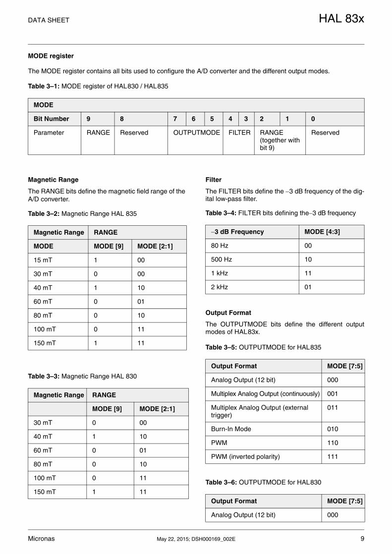
MODE register
The MODE register contains all bits used to configure the A/D converter and the different output modes.
Magnetic Range
The RANGE bits define the magnetic field range of the A/D converter.
Filter
The FILTER bits define the 3 dB frequency of the dig-ital low-pass filter.
Output Format
The OUTPUTMODE bits define the different outputmodes of HAL83x.
Table 3–1: MODE register of HAL830 / HAL835
MODE
Bit Number 9 8 7 6 5 4 3 2 1 0
Parameter RANGE Reserved OUTPUTMODE FILTER RANGE(together with bit 9)
Reserved
Table 3–2: Magnetic Range HAL 835
Magnetic Range RANGE
MODE MODE [9] MODE [2:1]
15 mT 1 00
30 mT 0 00
40 mT 1 10
60 mT 0 01
80 mT 0 10
100 mT 0 11
150 mT 1 11
Table 3–3: Magnetic Range HAL 830
Magnetic Range RANGE
MODE [9] MODE [2:1]
30 mT 0 00
40 mT 1 10
60 mT 0 01
80 mT 0 10
100 mT 0 11
150 mT 1 11
Table 3–4: FILTER bits defining the3 dB frequency
3 dB Frequency MODE [4:3]
80 Hz 00
500 Hz 10
1 kHz 11
2 kHz 01
Table 3–5: OUTPUTMODE for HAL835
Output Format MODE [7:5]
Analog Output (12 bit) 000
Multiplex Analog Output (continuously) 001
Multiplex Analog Output (external trigger)
011
Burn-In Mode 010
PWM 110
PWM (inverted polarity) 111
Table 3–6: OUTPUTMODE for HAL830
Output Format MODE [7:5]
Analog Output (12 bit) 000
HAL 83x DATA SHEET
10 May 22, 2015; DSH000169_002E Micronas
In Analog Output mode the sensor provides an ratio-metric 12 bit analog output voltage between 0 V and5 V.
In Multiplex Analog Output mode the sensor deliverstwo analog 7-bit values. The LSN (least significant nib-ble) and MSN of the output value are transmitted sepa-rately. This enables the sensor to transmit a 14-bit sig-nal to the 8-bit A/D converter of an ECU with theadvantage of achieving a higher signal-to-noise ratio ina disturbed environment.
– In external trigger mode the ECU can switch the out-put of the sensor between LSN and MSN by chang-ing the current flow direction through the sensor’s output. In case the output is pulled up by a 10 k resistor, the sensor sends the MSN. If the output is pulled down, the sensor will send the LSN. Maxi-mum refresh rate is about 500 Hz (2 ms).
– In continuous mode the sensor transmits first LSN and then MSN continuously and the ECU must lis-ten to the data stream sent by the sensor.
In the Multiplex Analog Output mode 1 LSB is repre-sented by a voltage level change of 39 mV. In AnalogOutput mode with14 bit 1 LSB would be 0.31 mV.
In Burn-In Mode the signal path of the sensors DSP isstimulated internally without applied magnetic field. Inthis mode the sensor provides a “saw tooth” shapeoutput signal. Shape and frequency of the saw toothsignal depend on the programming of the sensor.This mode can be used for Burn-In test in the custom-ers production line.
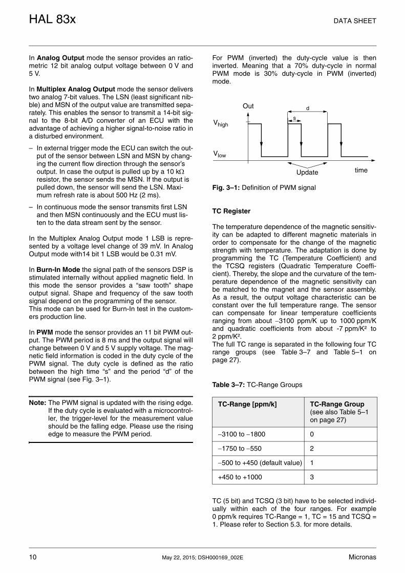
In PWM mode the sensor provides an 11 bit PWM out-put. The PWM period is 8 ms and the output signal willchange between 0 V and 5 V supply voltage. The mag-netic field information is coded in the duty cycle of thePWM signal. The duty cycle is defined as the ratiobetween the high time “s” and the period “d” of thePWM signal (see Fig. 3–1).
Note: The PWM signal is updated with the rising edge.If the duty cycle is evaluated with a microcontrol-ler, the trigger-level for the measurement valueshould be the falling edge. Please use the risingedge to measure the PWM period.
For PWM (inverted) the duty-cycle value is theninverted. Meaning that a 70% duty-cycle in normalPWM mode is 30% duty-cycle in PWM (inverted)mode.
Fig. 3–1: Definition of PWM signal
TC Register
The temperature dependence of the magnetic sensitiv-ity can be adapted to different magnetic materials inorder to compensate for the change of the magneticstrength with temperature. The adaptation is done byprogramming the TC (Temperature Coefficient) andthe TCSQ registers (Quadratic Temperature Coeffi-cient). Thereby, the slope and the curvature of the tem-perature dependence of the magnetic sensitivity canbe matched to the magnet and the sensor assembly.As a result, the output voltage characteristic can beconstant over the full temperature range. The sensorcan compensate for linear temperature coefficientsranging from about 3100 ppm/K up to 1000 ppm/Kand quadratic coefficients from about -7 ppm/K² to2 ppm/K². The full TC range is separated in the following four TCrange groups (see Table 3–7 and Table 5–1 onpage 27).
TC (5 bit) and TCSQ (3 bit) have to be selected individ-ually within each of the four ranges. For example0 ppm/k requires TC-Range = 1, TC = 15 and TCSQ =1. Please refer to Section 5.3. for more details.
Table 3–7: TC-Range Groups
TC-Range [ppm/k] TC-Range Group(see also Table 5–1 on page 27)
3100 to 1800 0
1750 to 550 2
500 to +450 (default value) 1
+450 to +1000 3
Update
Out
time
Vhigh
Vlow
d
s
DATA SHEET HAL 83x
Micronas May 22, 2015; DSH000169_002E 11
Sensitivity
The SENSITIVITY register contains the parameter forthe multiplier in the DSP. The Sensitivity is programma-ble between 4 and 4. For VSUP = 5 V, the register canbe changed in steps of 0.00049.
For all calculations, the digital value from the magneticfield of the D/A converter is used. This digital informa-tion is readable from the D/A-READOUT register.
VOQ
The VOQ register contains the parameter for the adderin the DSP. VOQ is the output signal without externalmagnetic field (B = 0 mT) and programmable fromVSUP (100% duty-cycle) up to VSUP (100% duty-cycle). For VSUP = 5 V, the register can be changed insteps of 4.9 mV (0.05% duty-cycle).
Note: If VOQ is programmed to a negative value, themaximum output signal is limited to:
Clamping Levels
The output signal range can be clamped in order todetect failures like shorts to VSUP or GND or an opencircuit.
The CLAMP-LOW register contains the parameter forthe lower limit. The lower clamping limit is programma-ble between 0 V (min. duty-cycle) and VSUP/2 (50%duty-cycle). For VSUP = 5 V, the register can bechanged in steps of 9.77 mV (0.195% duty-cycle).
The CLAMP-HIGH register contains the parameter forthe upper limit. The upper clamping voltage is pro-grammable between 0 V (min. duty-cycle) and VSUP(max. duty-cycle). For VSUP = 5 V, in steps of 9.77 mV(0.195% duty-cycle).
GP Register
This register can be used to store some information,like production date or customer serial number.Micronas will store production Lot number, wafer num-ber and x,y coordinates in registers GP1 to GP3. Thetotal register contains of four blocks with a length of 13bit each.The customer can read out this informationand store it in his production data base for reference orhe can store own production information instead.
Note: This register is not a guarantee for traceability.
To read/write this register it is mandatory toread/write all GP register one after the otherstarting with GP0. In case of writing the regis-ters it is necessary to first write all registers fol-lowed by one store sequence at the end. Even ifonly GP0 should be changed all other GP regis-ters must first be read and the read out datamust be written again to these registers.
LOCK
By setting the 1-bit register all registers will be lockedand the sensor will no longer respond to any supplyvoltage modulation. This bit is active after the firstpower-off and power-on sequence after setting theLOCK bit.
Warning: This register cannot be reset!
D/A-READOUT
This 14-bit register delivers the actual digital value ofthe applied magnetic field after the signal processing.This register can be read out and is the basis for thecalibration procedure of the sensor in the system envi-ronment.
Note: The MSB and LSB are reversed compared withall the other registers. Please reverse this regis-ter after readout.
Note: HAL835: During calibration it is mandatory toselect the Analog Output as output format. TheD/A-Readout register can be read out only in theAnalog Output mode. For all other modes theresult read back from the sensor will be a 0.After the calibration the output format can thaneasily be switched to the wanted output mode,like PWM.
SENSITIVITYVOUT 16383
DA Readout VDD– -------------------------------------------------------------- SensINITIAL=
VOUTmax VOQ VSUP+=
HAL 83x DATA SHEET
12 May 22, 2015; DSH000169_002E Micronas
3.3. Calibration Procedure
3.3.1. General Procedure
For calibration in the system environment, the applica-tion kit from Micronas is recommended. It contains thehardware for generation of the serial telegram for pro-gramming (Programmer Board Version 5.1) and thecorresponding software (PC83x) for the input of theregister values.
For the individual calibration of each sensor in the cus-tomer application, a two point adjustment is recom-mended. The calibration shall be done as follows:
Step 1: Input of the registers which need not be adjusted individually
The magnetic circuit, the magnetic material with itstemperature characteristics, the filter frequency, theoutput mode and the GP register value are given forthis application. Therefore, the values of the followingregister blocks should be identical for all sensors of thecustomer application.
– FILTER (according to the maximum signal frequency)
– RANGE(according to the maximum magnetic field at the sensor position)
– OUTPUTMODE
– TC, TCSQ and TC-RANGE(depends on the material of the magnet and the other temperature dependencies of the application)
– GP(if the customer wants to store own production infor-mation. It is not necessary to change this register)
As the clamping levels are given. They have an influ-ence on the D/A-Readout value and have to be settherefore after the adjustment process.
Write the appropriate settings into the HAL83x regis-ters.
Step 2: Initialize DSP
As the D/A-READOUT register value depends onthe settings of SENSITIVITY, VOQ and CLAMP-LOW/HIGH, these registers have to be initializedwith defined values, first:
– VOQINITIAL = 2.5 V
– Clamp-Low = 0 V
– Clamp-High = 4.999 V
– SensINITIAL (see table 3-1.)
Step 3: Define Calibration Points
The calibration points 1 and 2 can be set inside thespecified range. The corresponding values for VOUT1and VOUT2 result from the application requirements.
For highest accuracy of the sensor, calibration pointsnear the minimum and maximum input signal are rec-ommended. The difference of the output voltagebetween calibration point 1 and calibration point 2should be more than 3.5 V.
Table 3–1:
3dB Filter frequency SensINITIAL
80 Hz 0.6
500 Hz 0.39
1 kHz 0.42
2 kHz 0.83
Lowclampingvoltage VOUT1,2 Highclampingvoltage
DATA SHEET HAL 83x
Micronas May 22, 2015; DSH000169_002E 13
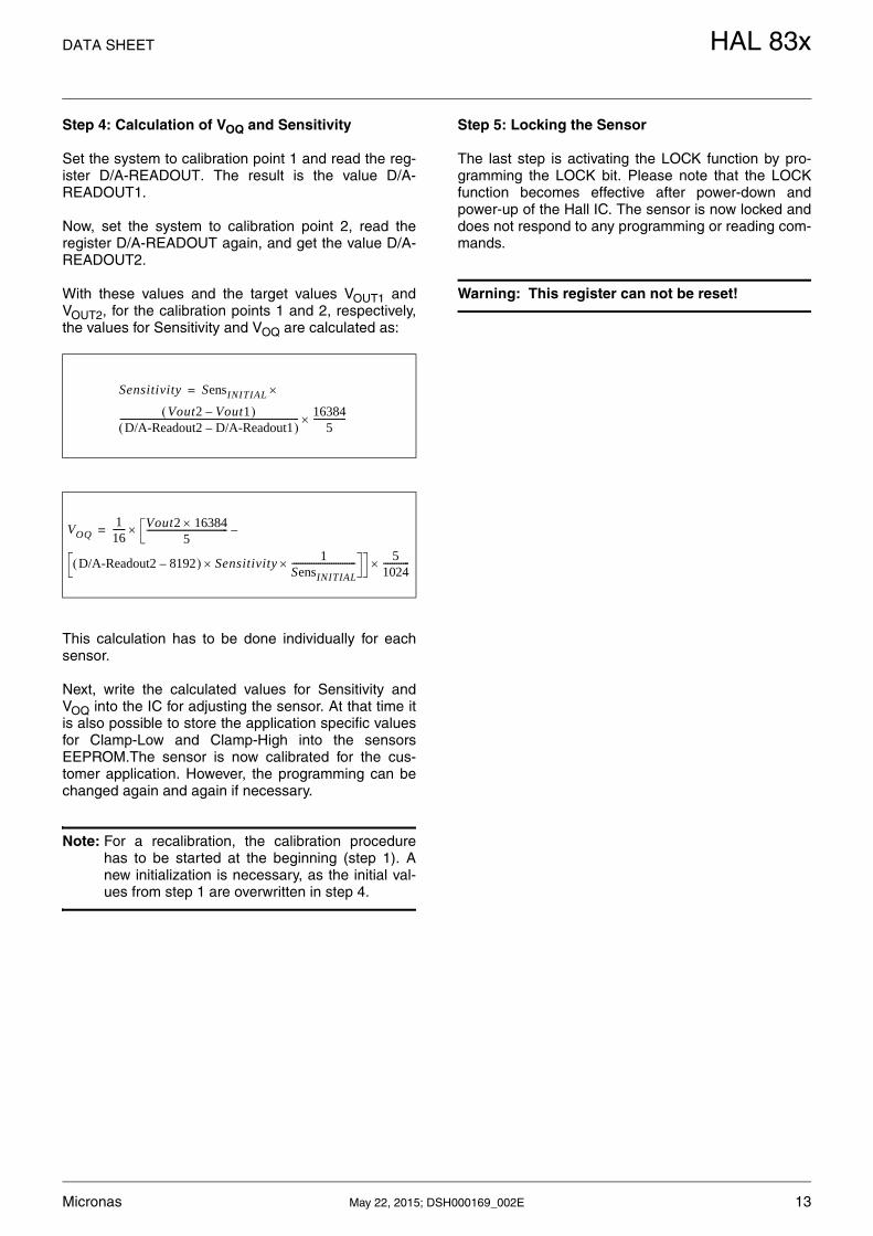
Step 4: Calculation of VOQ and Sensitivity
Set the system to calibration point 1 and read the reg-ister D/A-READOUT. The result is the value D/A-READOUT1.
Now, set the system to calibration point 2, read theregister D/A-READOUT again, and get the value D/A-READOUT2.
With these values and the target values VOUT1 andVOUT2, for the calibration points 1 and 2, respectively,the values for Sensitivity and VOQ are calculated as:
This calculation has to be done individually for eachsensor.
Next, write the calculated values for Sensitivity andVOQ into the IC for adjusting the sensor. At that time itis also possible to store the application specific valuesfor Clamp-Low and Clamp-High into the sensorsEEPROM.The sensor is now calibrated for the cus-tomer application. However, the programming can bechanged again and again if necessary.
Note: For a recalibration, the calibration procedurehas to be started at the beginning (step 1). Anew initialization is necessary, as the initial val-ues from step 1 are overwritten in step 4.
Step 5: Locking the Sensor
The last step is activating the LOCK function by pro-gramming the LOCK bit. Please note that the LOCKfunction becomes effective after power-down andpower-up of the Hall IC. The sensor is now locked anddoes not respond to any programming or reading com-mands.
Warning: This register can not be reset!
Sensitivity SensINITIAL
Vout2 Vout1– D/A-Readout2 D/A-Readout1–
---------------------------------------------------------------------------------
163845
---------------
=
VOQ116------ Vout2 16384
5-------------------------------------
D/A-Readout2 8192– Sensitivity 1SensINITIAL-----------------------------
–
51024------------
=
HAL 83x DATA SHEET
14 May 22, 2015; DSH000169_002E Micronas
4. Specifications
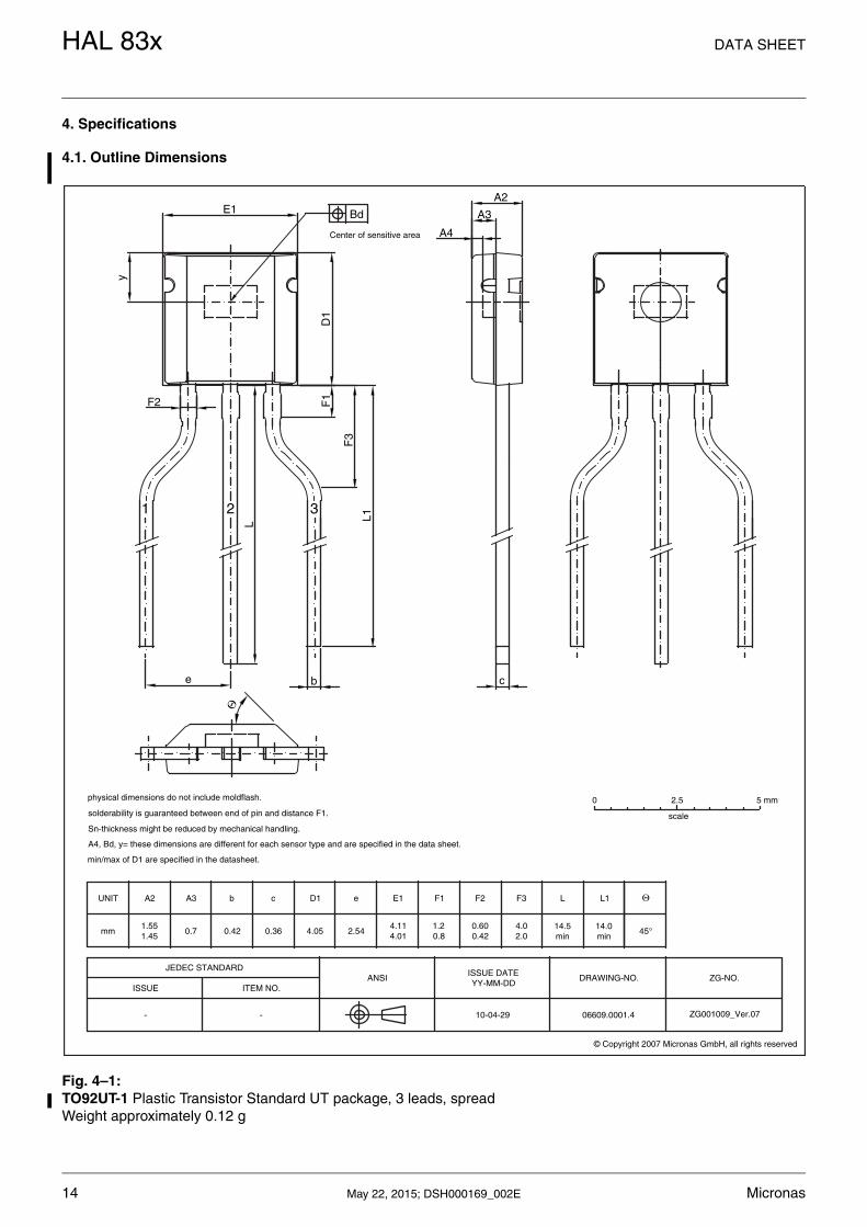
4.1. Outline Dimensions
Fig. 4–1:TO92UT-1 Plastic Transistor Standard UT package, 3 leads, spreadWeight approximately 0.12 g
© Copyright 2007 Micronas GmbH, all rights reserved
ISSUE DATEYY-MM-DD
ITEM NO.
solderability is guaranteed between end of pin and distance F1.
A4, Bd, y= these dimensions are different for each sensor type and are specified in the data sheet.
-
JEDEC STANDARD
ISSUE
UNIT
mm
A2
1.551.45
A3
0.7
ANSI
- 10-04-29
0.36
b
0.42
c D1
4.05
E1
4.114.01
e
2.54
F1
1.20.8
5 mm
06609.0001.4
DRAWING-NO.
ZG001009_Ver.07
ZG-NO.
L1
14.0min
F3F2
0.600.42
4.02.0
L
14.5min
0
scale
Θ
45°
2.5
A2
c
D1
L
e
Θ
F2
L1
b
F3
F1
E1
y
Center of sensitive area
Bd A3
A4
physical dimensions do not include moldflash.
min/max of D1 are specified in the datasheet.
Sn-thickness might be reduced by mechanical handling.
1 2 3
DATA SHEET HAL 83x
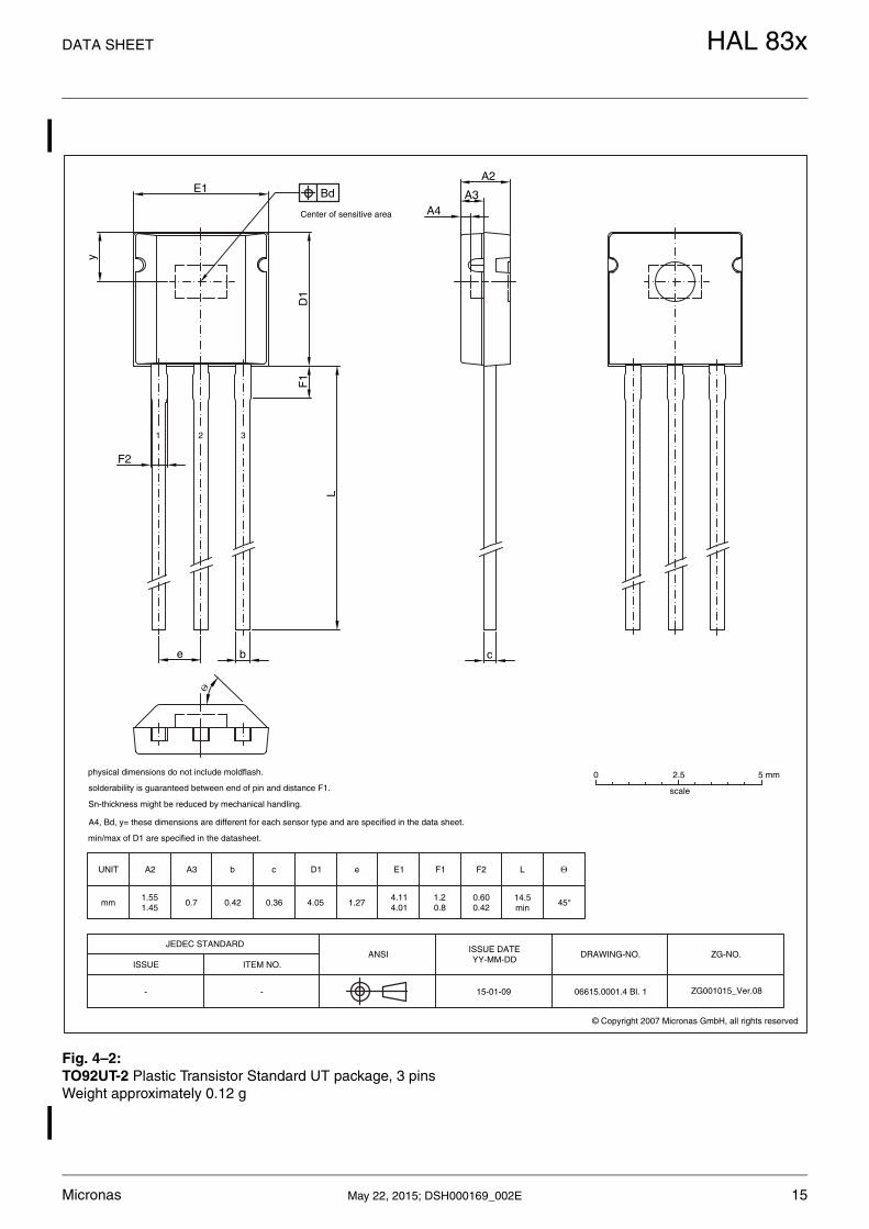
Micronas May 22, 2015; DSH000169_002E 15
Fig. 4–2:TO92UT-2 Plastic Transistor Standard UT package, 3 pinsWeight approximately 0.12 g
© Copyright 2007 Micronas GmbH, all rights reserved
Θ
DRAWING-NO.
06615.0001.4 Bl. 1
solderability is guaranteed between end of pin and distance F1.
A4, Bd, y= these dimensions are different for each sensor type and are specified in the data sheet.
0.36mm1.551.45
0.7 0.42
JEDEC STANDARD
ISSUE
-
ITEM NO.
-
A3UNIT A2 b c
4.054.114.01
1.20.8
0.600.42
1.2714.5min
ANSI
15-01-09
ISSUE DATEYY-MM-DD
D1 e E1 F2F1 L
45°
ZG-NO.
ZG001015_Ver.08
2.50
Θ
scale
5 mm
D1
L
e b
F2
1 2 3
F1
c
Bd
Center of sensitive area
E1
y
A4
A2
A3
physical dimensions do not include moldflash.
min/max of D1 are specified in the datasheet.
Sn-thickness might be reduced by mechanical handling.
HAL 83x DATA SHEET
16 May 22, 2015; DSH000169_002E Micronas
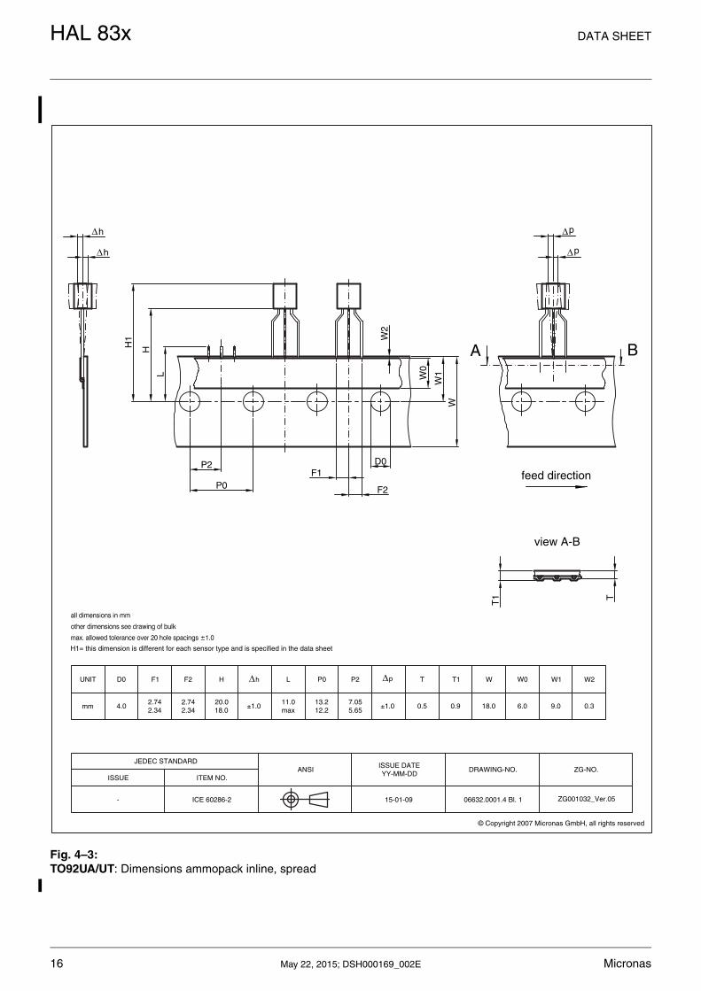
Fig. 4–3:TO92UA/UT: Dimensions ammopack inline, spread
© Copyright 2007 Micronas GmbH, all rights reserved
p
p
feed direction
T1
mm
UNIT P0
13.212.2
ITEM NO.
ICE 60286-2
ISSUE
-
2.742.34
JEDEC STANDARD
4.02.742.34
20.018.0
±1.0
ANSI
11.0max
F1D0 F2 H Δh L
ISSUE DATEYY-MM-DD
15-01-09
7.055.65
±1.0 0.5
06632.0001.4 Bl. 1
18.0
DRAWING-NO.
0.9 6.0
P2 Δp T T1 W W0
view A-B
Δ
h
h
Δ
F1
H
L
P0
P2
W
W1
A
D0
F2
ZG001032_Ver.05
ZG-NO.
T
B
Δ
Δ
9.0
W1
0.3
W2
H1 W
2
W0
H1= this dimension is different for each sensor type and is specified in the data sheet
DATA SHEET HAL 83x
Micronas May 22, 2015; DSH000169_002E 17
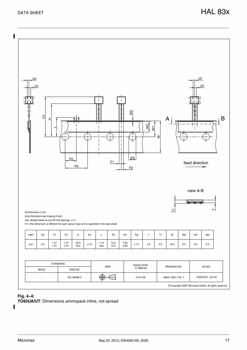
Fig. 4–4:TO92UA/UT: Dimensions ammopack inline, not spread
© Copyright 2007 Micronas GmbH, all rights reserved
p
p
feed direction
T1
mm
UNIT P0
13.212.2
ITEM NO.
IEC 60286-2
ISSUE
-
1.471.07
STANDARD
4.01.471.07
20.018.0
±1.0
ANSI
11.0max
F1D0 F2 H Δh L
ISSUE DATEYY-MM-DD
15-01-09
7.055.65
±1.0 0.5
06631.0001.4 Bl. 1
18.0
DRAWING-NO.
0.9 6.0
P2 Δp T T1 W W0
view A-B
Δ
h
h
Δ
F1
H
L
P0
P2W
W1
A
D0
F2
ZG001031_Ver.04
ZG-NO.
T
B
Δ
Δ
9.0 0.3
W1 W2
H1 W
2
W0
H1= this dimension is different for each sensor type and is specified in the data sheet
HAL 83x DATA SHEET
18 May 22, 2015; DSH000169_002E Micronas
4.2. Soldering, Welding and Assembly
Information related to solderability, welding, assembly, and second-level packaging is included in the document“Guidelines for the Assembly of Micronas Packages”. It is available on the Micronas website or on the service portal.
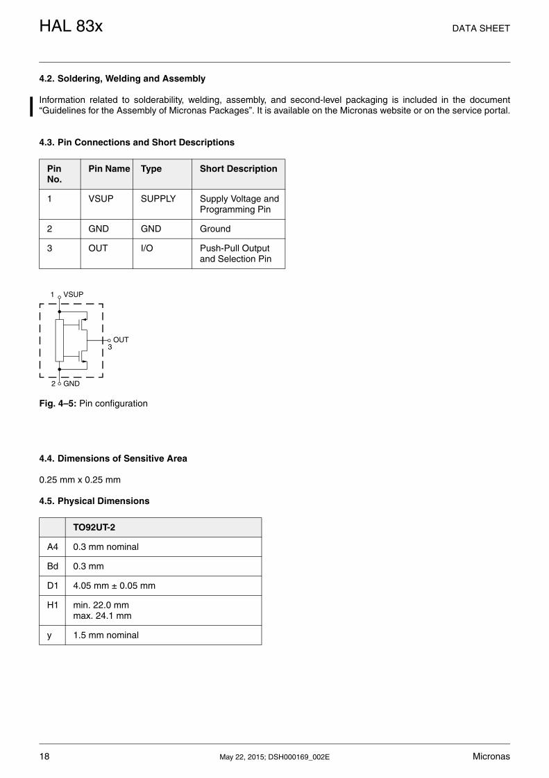
4.3. Pin Connections and Short Descriptions
Fig. 4–5: Pin configuration
4.4. Dimensions of Sensitive Area
0.25 mm x 0.25 mm
4.5. Physical Dimensions
Pin No.
Pin Name Type Short Description
1 VSUP SUPPLY Supply Voltage andProgramming Pin
2 GND GND Ground
3 OUT I/O Push-Pull Output and Selection Pin
1
2
3
VSUP
OUT
GND
TO92UT-2
A4 0.3 mm nominal
Bd 0.3 mm
D1 4.05 mm ± 0.05 mm
H1 min. 22.0 mmmax. 24.1 mm
y 1.5 mm nominal
DATA SHEET HAL 83x
Micronas May 22, 2015; DSH000169_002E 19
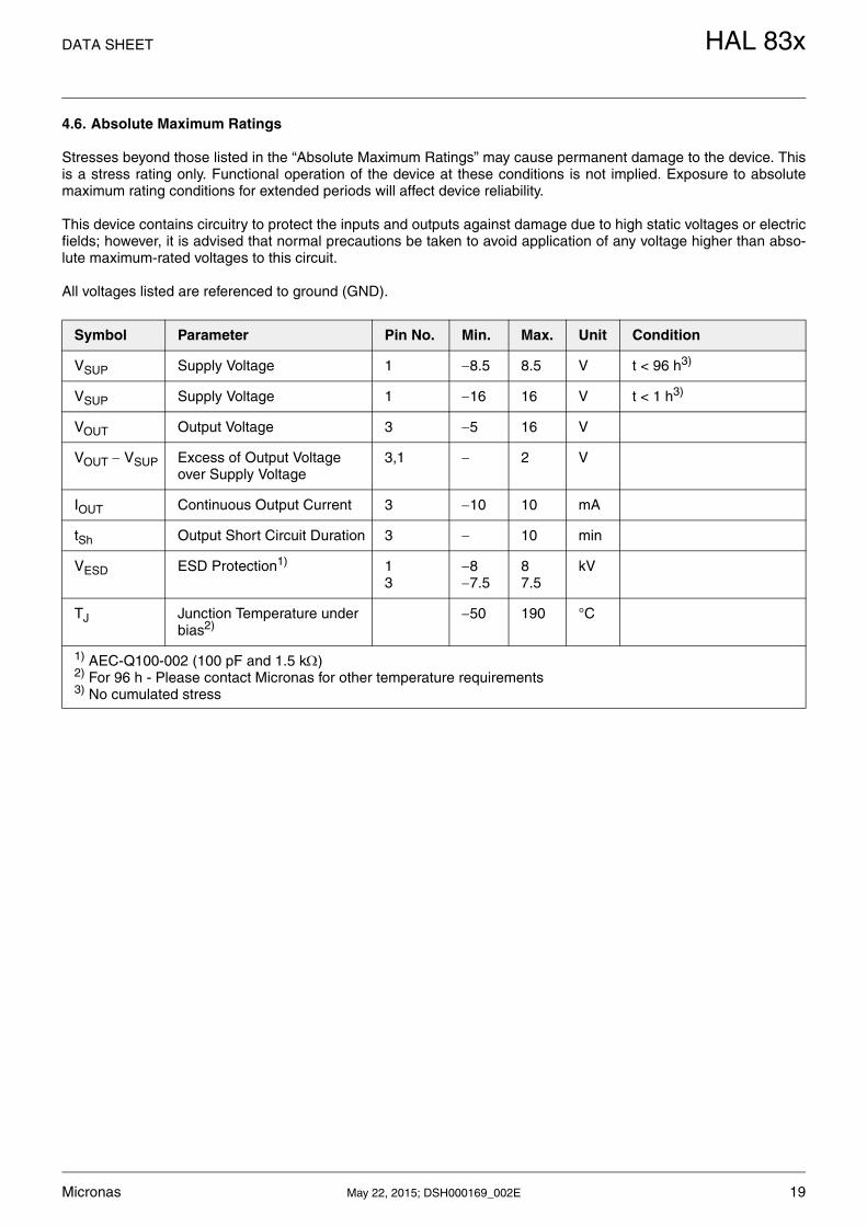
4.6. Absolute Maximum Ratings
Stresses beyond those listed in the “Absolute Maximum Ratings” may cause permanent damage to the device. Thisis a stress rating only. Functional operation of the device at these conditions is not implied. Exposure to absolutemaximum rating conditions for extended periods will affect device reliability.
This device contains circuitry to protect the inputs and outputs against damage due to high static voltages or electricfields; however, it is advised that normal precautions be taken to avoid application of any voltage higher than abso-lute maximum-rated voltages to this circuit.
All voltages listed are referenced to ground (GND).
Symbol Parameter Pin No. Min. Max. Unit Condition
VSUP Supply Voltage 1 8.5 8.5 V t < 96 h3)
VSUP Supply Voltage 1 16 16 V t < 1 h3)
VOUT Output Voltage 3 5 16 V
VOUT VSUP Excess of Output Voltage over Supply Voltage
3,1 2 V
IOUT Continuous Output Current 3 10 10 mA
tSh Output Short Circuit Duration 3 10 min
VESD ESD Protection1) 13
87.5
87.5
kV
TJ Junction Temperature under bias2)
50 190 °C
1) AEC-Q100-002 (100 pF and 1.5 k)2) For 96 h - Please contact Micronas for other temperature requirements3) No cumulated stress
HAL 83x DATA SHEET
20 May 22, 2015; DSH000169_002E Micronas
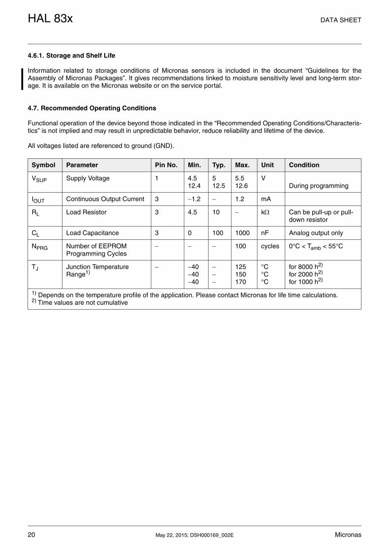
4.6.1. Storage and Shelf Life
Information related to storage conditions of Micronas sensors is included in the document “Guidelines for theAssembly of Micronas Packages”. It gives recommendations linked to moisture sensitivity level and long-term stor-age. It is available on the Micronas website or on the service portal.
4.7. Recommended Operating Conditions
Functional operation of the device beyond those indicated in the “Recommended Operating Conditions/Characteris-tics” is not implied and may result in unpredictable behavior, reduce reliability and lifetime of the device.
All voltages listed are referenced to ground (GND).
Symbol Parameter Pin No. Min. Typ. Max. Unit Condition
VSUP Supply Voltage 1 4.512.4
512.5
5.512.6
VDuring programming
IOUT Continuous Output Current 3 1.2 1.2 mA
RL Load Resistor 3 4.5 10 k Can be pull-up or pull-down resistor
CL Load Capacitance 3 0 100 1000 nF Analog output only
NPRG Number of EEPROMProgramming Cycles
100 cycles 0°C < Tamb < 55°C
TJ Junction Temperature Range1)
404040
125150170
°C°C°C
for 8000 h2) for 2000 h2)
for 1000 h2)
1) Depends on the temperature profile of the application. Please contact Micronas for life time calculations.2) Time values are not cumulative
DATA SHEET HAL 83x
Micronas May 22, 2015; DSH000169_002E 21
4.8. Characteristics
at TJ = 40 °C to +170 °C, VSUP = 4.5 V to 5.5 V, GND = 0 V after programming and locking, at RecommendedOperation Conditions if not otherwise specified in the column “Conditions”.Typical Characteristics for TJ = 25 °C and VSUP = 5 V.
Symbol Parameter Pin No. Min. Typ. Max. Unit Conditions
ISUP Supply Current over Temperature Range
1 5 7 10 mA
ES Error in Magnetic Sensitivity over Temperature Range5)
3 41
00
41
% HAL830HAL835VSUP = 5 V; 60 mT range, 3db
frequency = 500 Hz, TC & TCSQ for linearized temperature coefficients(see Section 4.8.1. on page 23)
Analog Output (HAL830 & HAL835)
Resolution 3 12 bit ratiometric to VSUP 1)
DNL Differential Non-Linearity of D/A converter2)
3 2.01.5
00
2.01.5
LSB HAL830HAL835
Only @ 25°C ambient temperature
INL Non-Linearity of Output Voltage over Temperature
3 0.5 0 0.5 % % of supply voltage3)
For VOUT = 0.35 V ... 4.65 V;VSUP = 5 V, Sensitivity 0.95
ER Ratiometric Error of Output over Temperature (Error in VOUT / VSUP)
3 0.25 0 0.25 % VOUT1 - VOUT2> 2 Vduring calibration procedure
VOffset Offset Drift over Temperature RangeVOUT(B = 0 mT)25°C- VOUT(B = 0 mT)max
5)
3 0.60.2
0.250.1
0.60.2
% VSUP HAL830HAL835
VSUP = 5 V; 60 mT range,3dB frequency = 500 Hz, TC = 15, TCSQ = 1, TC-Range = 1
0.65 < sensitivity < 0.65
VOUTCL Accuracy of Output Voltage at Clamping Low Voltage over Temperature Range
3 15 0 15 mV RL = 5 k, VSUP = 5 VSpec values are derived from resolutions of the registers Clamp-Low/Clamp-High and the parameter VoffsetVOUTCH Accuracy of Output Voltage at
Clamping High Voltage over Temperature Range
3 15 0 15 mV
VOUTH Upper Limit of Signal Band4) 3 4.65 4.8 V VSUP = 5 V, 1 mA IOUT 1mA
VOUTL Lower Limit of Signal Band4) 3 0.2 0.35 V VSUP = 5 V, 1 mA IOUT 1mA
ROUT Output Resistance over Recommended Operating Range
3 1 10 VOUTLmax VOUT VOUTHmin
tr(O) Step Response Time of Output6) 3 3.01.51.10.9
ms 3 dB Filter frequency = 80 Hz3 dB Filter frequency = 500 Hz3 dB Filter frequency = 1 kHz3 dB Filter frequency = 2kHzCL = 10 nF, time to 90% of final output voltage for a steplike signal Bstep from 0 mT to Bmax
tPOD Power-Up Time (Time to reach stable Output Voltage)
1.5 1.7 1.9 ms CL = 10 nF, 90% of VOUT
1) Output DAC full scale = 5 V ratiometric, Output DAC offset = 0 V, Output DAC LSB = VSUP/40962) Only tested at 25°C. The specified values are test limits only. Overmolding and packaging might influence this parameter3) If more than 50% of the selected magnetic field range is used (Sensitivity 0.5) and the temperature compensation is suitable.
INL = VOUT VOUTLSF = Least Square Fit Line voltage based on VOUT measurements at a fixed temperature.4) Signal Band Area with full accuracy is located between VOUTL and VOUTH. The sensor accuracy is reduced below VOUTL and above VOUTH5) Tambient = 150°C6) Guaranteed by design
HAL 83x DATA SHEET
22 May 22, 2015; DSH000169_002E Micronas
Symbol Parameter Pin No. Min. Typ. Max. Unit Conditions
BW Small Signal Bandwidth (3 dB) 3 2 kHz BAC < 10 mT;3 dB Filter frequency = 2 kHz
VOUTn Noise Output VoltageRMS 3 1 5 mV magnetic range = 60 mT3 dB Filter frequency = 500 HzSensitivity 0.7; C = 4.7 nF (VSUP & VOUT to GND)
DACGE D/A-Converter Glitch Energy 3 40 nV 7)
PWM Output (HAL835 only)
Resolution 3 11 bit
DCMIN-DUTY
Accuracy of Duty Cycle at Clamp Low over Temperature Range
3 0.3 0 0.3 % Spec values are derived from resolutions of the registers Clamp-Low/Clamp-High and the parameter DCOQoffsetDCMAX-
DUTY
Accuracy of Duty Cycle at Clamp High over Temperature Range
3 0.3 0 0.3 %
VOUTH Output High Voltage 3 4.8 V VSUP = 5 V, 1 mA IOUT 1mA
VOUTL Output Low Voltage 3 0.2 V VSUP = 5 V, 1 mA IOUT 1mA
fPWM PWM Output Frequency over Temperature Range
3 105 125 145 Hz
tPOD Power-Up Time (Time to reach valid Duty Cycle)
3 8.5 ms
tr(O) Step Response Time of Output 3 30,90,60,4
1,20.80,5
ms 3 dB Filter frequency = 80 Hz3 dB Filter frequency = 500 Hz3 dB Filter frequency = 1 kHz3 dB Filter frequency = 2kHzTime to 90% of final output voltage for a steplike signal Bstep from 0 mT to Bmax
TO92UT Packages
Rthja
Rthjc
Thermal Resistance
junction to air
junction to case
235
61
K/W
K/W
Measured with a 1s0p board
Measured with a 1s0p board
7) The energy of the impulse injected into the analog output when the code in the D/A-Converter register changes state. This energy is normally specified as the area of the glitch in nVs.
DATA SHEET HAL 83x
Micronas May 22, 2015; DSH000169_002E 23
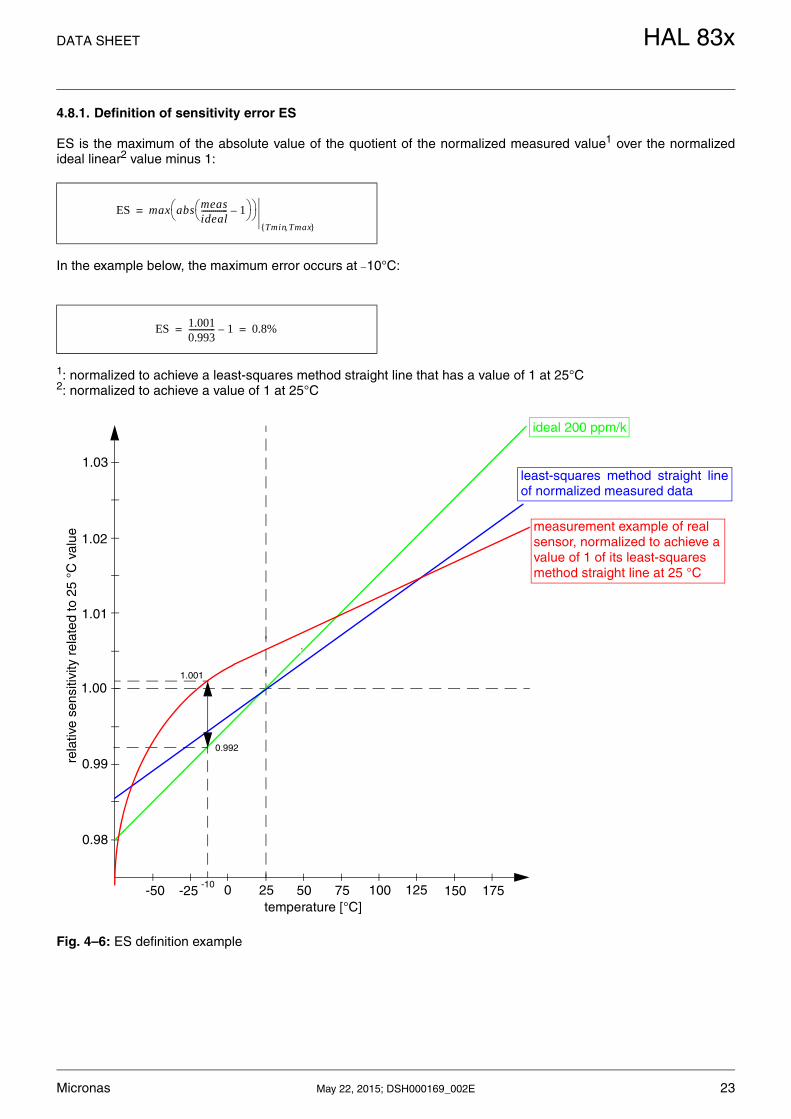
4.8.1. Definition of sensitivity error ES
ES is the maximum of the absolute value of the quotient of the normalized measured value1 over the normalizedideal linear2 value minus 1:
In the example below, the maximum error occurs at 10°C:
1: normalized to achieve a least-squares method straight line that has a value of 1 at 25°C2: normalized to achieve a value of 1 at 25°C
Fig. 4–6: ES definition example
ES max abs measideal------------- 1–
Tmin Tmax{ , }
=
ES 1.0010.993------------- 1– 0.8%= =
50 75 100 125 150 175250-25-50
0.98
0.99
1.00
1.01
1.02
1.03
-10
0.992
1.001
temperature [°C]
rela
tive
sens
itivi
ty r
elat
ed to
25
°C v
alue
ideal 200 ppm/k
measurement example of realsensor, normalized to achieve avalue of 1 of its least-squaresmethod straight line at 25 °C
least-squares method straight lineof normalized measured data
HAL 83x DATA SHEET
24 May 22, 2015; DSH000169_002E Micronas
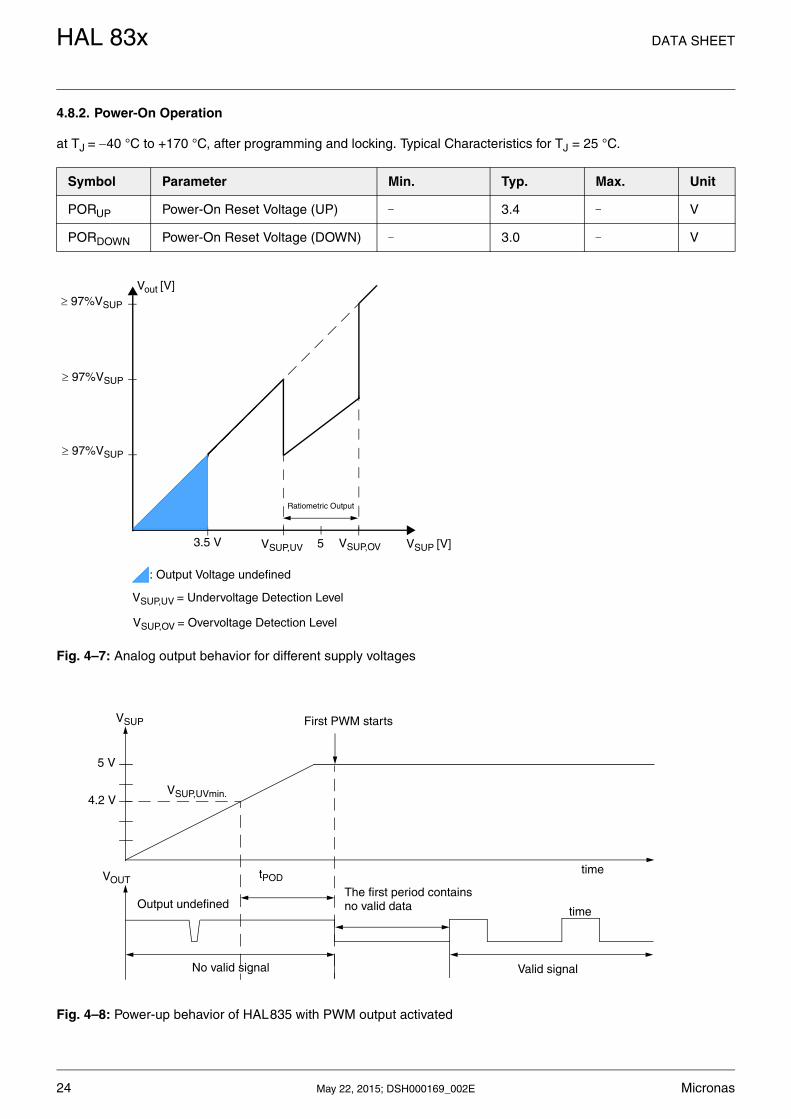
4.8.2. Power-On Operation
at TJ = 40 °C to +170 °C, after programming and locking. Typical Characteristics for TJ = 25 °C.
Fig. 4–7: Analog output behavior for different supply voltages
Fig. 4–8: Power-up behavior of HAL835 with PWM output activated
Symbol Parameter Min. Typ. Max. Unit
PORUP Power-On Reset Voltage (UP) 3.4 V
PORDOWN Power-On Reset Voltage (DOWN) 3.0 V
VSUP,UV 5 VSUP,OV VSUP [V]
Vout [V]
97%VSUP
97%VSUP
: Output Voltage undefined
3.5 V
97%VSUP
Ratiometric Output
VSUP,UV = Undervoltage Detection Level
VSUP,OV = Overvoltage Detection Level
First PWM starts
timeVOUT
VSUP
5 V
tPOD
Output undefinedtime
No valid signal Valid signal
The first period containsno valid data
4.2 VVSUP,UVmin.
DATA SHEET HAL 83x
Micronas May 22, 2015; DSH000169_002E 25
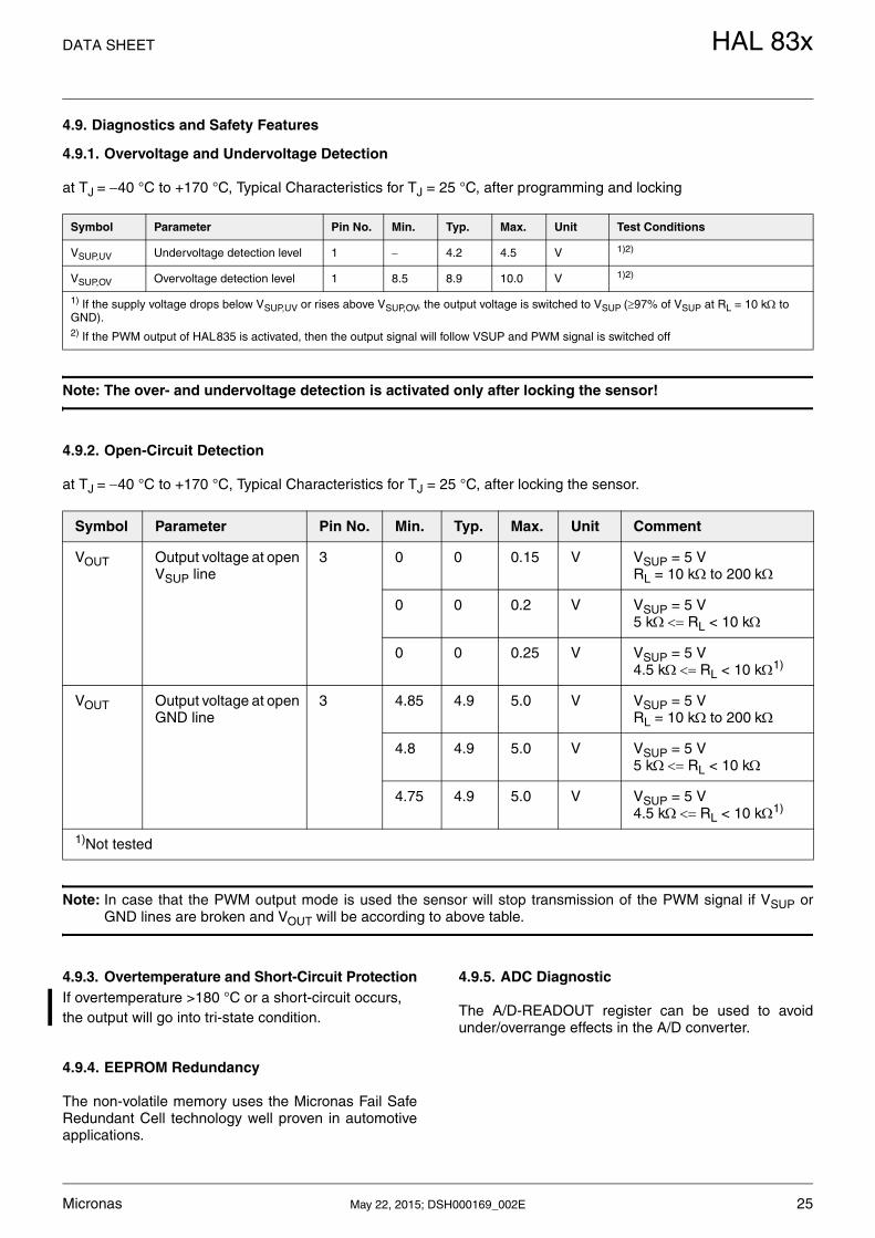
4.9. Diagnostics and Safety Features
4.9.1. Overvoltage and Undervoltage Detection
at TJ = 40 °C to +170 °C, Typical Characteristics for TJ = 25 °C, after programming and locking
Note: The over- and undervoltage detection is activated only after locking the sensor!
4.9.2. Open-Circuit Detection
at TJ = 40 °C to +170 °C, Typical Characteristics for TJ = 25 °C, after locking the sensor.
Note: In case that the PWM output mode is used the sensor will stop transmission of the PWM signal if VSUP orGND lines are broken and VOUT will be according to above table.
4.9.3. Overtemperature and Short-Circuit ProtectionIf overtemperature >180 °C or a short-circuit occurs, the output will go into tri-state condition.
4.9.4. EEPROM Redundancy
The non-volatile memory uses the Micronas Fail SafeRedundant Cell technology well proven in automotiveapplications.
4.9.5. ADC Diagnostic
The A/D-READOUT register can be used to avoidunder/overrange effects in the A/D converter.
Symbol Parameter Pin No. Min. Typ. Max. Unit Test Conditions
VSUP,UV Undervoltage detection level 1 4.2 4.5 V 1)2)
VSUP,OV Overvoltage detection level 1 8.5 8.9 10.0 V 1)2)
1) If the supply voltage drops below VSUP,UV or rises above VSUP,OV, the output voltage is switched to VSUP (97% of VSUP at RL = 10 k to GND).2) If the PWM output of HAL835 is activated, then the output signal will follow VSUP and PWM signal is switched off
Symbol Parameter Pin No. Min. Typ. Max. Unit Comment
VOUT Output voltage at open VSUP line
3 0 0 0.15 V VSUP = 5 VRL = 10 kto 200k
0 0 0.2 V VSUP = 5 V5 kRL < 10 k
0 0 0.25 V VSUP = 5 V4.5 kRL < 10 k1)
VOUT Output voltage at open GND line
3 4.85 4.9 5.0 V VSUP = 5 VRL = 10 kto 200k
4.8 4.9 5.0 V VSUP = 5 V5 kRL < 10 k
4.75 4.9 5.0 V VSUP = 5 V4.5 kRL < 10 k1)
1)Not tested
HAL 83x DATA SHEET
26 May 22, 2015; DSH000169_002E Micronas
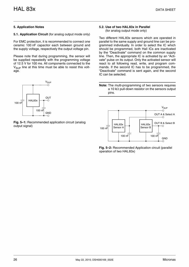
5. Application Notes
5.1. Application Circuit (for analog output mode only)
For EMC protection, it is recommended to connect oneceramic 100 nF capacitor each between ground andthe supply voltage, respectively the output voltage pin.
Please note that during programming, the sensor willbe supplied repeatedly with the programming voltageof 12.5 V for 100 ms. All components connected to theVSUP line at this time must be able to resist this volt-age.
Fig. 5–1: Recommended application circuit (analog output signal)
5.2. Use of two HAL83x in Parallel(for analog output mode only)
Two different HAL83x sensors which are operated inparallel to the same supply and ground line can be pro-grammed individually. In order to select the IC whichshould be programmed, both Hall ICs are inactivatedby the “Deactivate” command on the common supplyline. Then, the appropriate IC is activated by an “Acti-vate” pulse on its output. Only the activated sensor willreact to all following read, write, and program com-mands. If the second IC has to be programmed, the“Deactivate” command is sent again, and the secondIC can be selected.
Note: The multi-programming of two sensors requiresa 10 k pull-down resistor on the sensors outputpins.
Fig. 5–2: Recommended Application circuit (parallel operation of two HAL83x)
OUT
VSUP
GND
100 nFHAL83x
100 nF
HAL83x
GND
100 nF
HAL83x
100 nF 100 nF
Sensor A Sensor B
VSUP
OUT B & Select B
OUT A & Select A
DATA SHEET HAL 83x
Micronas May 22, 2015; DSH000169_002E 27
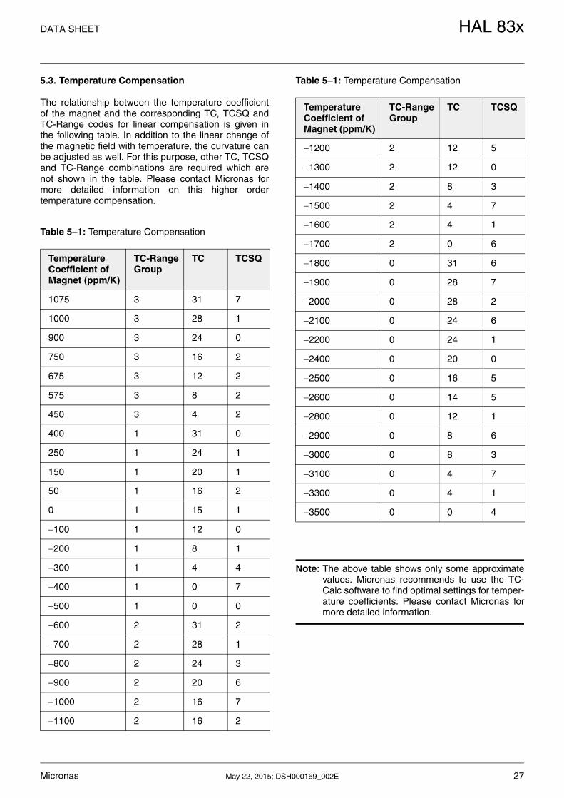
5.3. Temperature Compensation
The relationship between the temperature coefficientof the magnet and the corresponding TC, TCSQ andTC-Range codes for linear compensation is given inthe following table. In addition to the linear change ofthe magnetic field with temperature, the curvature canbe adjusted as well. For this purpose, other TC, TCSQand TC-Range combinations are required which arenot shown in the table. Please contact Micronas formore detailed information on this higher ordertemperature compensation.
Note: The above table shows only some approximatevalues. Micronas recommends to use the TC-Calc software to find optimal settings for temper-ature coefficients. Please contact Micronas formore detailed information.
Table 5–1: Temperature Compensation
Temperature Coefficient of Magnet (ppm/K)
TC-Range Group
TC TCSQ
1075 3 31 7
1000 3 28 1
900 3 24 0
750 3 16 2
675 3 12 2
575 3 8 2
450 3 4 2
400 1 31 0
250 1 24 1
150 1 20 1
50 1 16 2
0 1 15 1
100 1 12 0
200 1 8 1
300 1 4 4
400 1 0 7
500 1 0 0
600 2 31 2
700 2 28 1
800 2 24 3
900 2 20 6
1000 2 16 7
1100 2 16 2
1200 2 12 5
1300 2 12 0
1400 2 8 3
1500 2 4 7
1600 2 4 1
1700 2 0 6
1800 0 31 6
1900 0 28 7
2000 0 28 2
2100 0 24 6
2200 0 24 1
2400 0 20 0
2500 0 16 5
2600 0 14 5
2800 0 12 1
2900 0 8 6
3000 0 8 3
3100 0 4 7
3300 0 4 1
3500 0 0 4
Table 5–1: Temperature Compensation
Temperature Coefficient of Magnet (ppm/K)
TC-Range Group
TC TCSQ
HAL 83x DATA SHEET
28 May 22, 2015; DSH000169_002E Micronas
5.4. Ambient Temperature
Due to the internal power dissipation, the temperatureon the silicon chip (junction temperature TJ) is higherthan the temperature outside the package (ambienttemperature TA).
TJ = TA + T
At static conditions and continuous operation, the fol-lowing equation applies:
T = ISUP * VSUP * RthjX
The X represents junction-to-air or junction-to-case.
In order to estimate the temperature difference Tbetween the junction and the respective reference(e.g. air, case, or solder point) use the max. parame-ters for ISUP, RthX, and the max. value for VSUP fromthe application.
The following example shows the result for junction-to -air conditions. VSUP = 5.5 V, Rthja = 250 K/W andISUP = 10 mA the temperature difference T = 13.75 K.
The junction temperature TJ is specified. The maxi-mum ambient temperature TAmax can be estimated as:
TAmax = TJmax T
5.5. EMC and ESD
Please contact Micronas for the detailed investigationreports with the EMC and ESD results.
DATA SHEET HAL 83x
Micronas May 22, 2015; DSH000169_002E 29
6. Programming
6.1. Definition of Programming Pulses
The sensor is addressed by modulating a serial tele-gram on the supply voltage. The sensor answers with aserial telegram on the output pin.
The bits in the serial telegram have a different bit timefor the VSUP-line and the output. The bit time for theVSUP-line is defined through the length of the Sync Bitat the beginning of each telegram. The bit time for theoutput is defined through the Acknowledge Bit.
A logical “0” is coded as no voltage change within thebit time. A logical “1” is coded as a voltage changebetween 50% and 80% of the bit time. After each bit, avoltage change occurs.
6.2. Definition of the Telegram
Each telegram starts with the Sync Bit (logical 0), 3bits for the Command (COM), the Command Parity Bit(CP), 4 bits for the Address (ADR), and the AddressParity Bit (AP).
There are 4 kinds of telegrams:
– Write a register (see Fig. 6–2)After the AP Bit, follow 14 Data Bits (DAT) and theData Parity Bit (DP). If the telegram is valid and thecommand has been processed, the sensor answerswith an Acknowledge Bit (logical 0) on the output.
– Read a register (see Fig. 6–3)After evaluating this command, the sensor answerswith the Acknowledge Bit, 14 Data Bits, and theData Parity Bit on the output.
– Programming the EEPROM cells (see Fig. 6–4)After evaluating this command, the sensor answerswith the Acknowledge Bit. After the delay time tw,the supply voltage rises up to the programming volt-age.
– Activate a sensor (see Fig. 6–5)If more than one sensor is connected to the supplyline, selection can be done by first deactivating allsensors. The output of all sensors have to be pulledto ground. With an Activate pulse on the appropriateoutput pin, an individual sensor can be selected. Allfollowing commands will only be accepted from theactivated sensor.
Fig. 6–1: Definition of logical 0 and 1 bit
tr tf
tp0 tp0logical 0
VSUPH
VSUPL
or
tp0logical 1
VSUPH
VSUPL
ortp0
tp1
tp1
HAL 83x DATA SHEET
30 May 22, 2015; DSH000169_002E Micronas
Fig. 6–2: Telegram for coding a Write command
Fig. 6–3: Telegram for coding a Read command
Table 6–1: Telegram parameters
Symbol Parameter Pin Min. Typ. Max. Unit Remarks
VSUPL Supply Voltage for Low Levelduring Programming
1 5 5.6 6 V
VSUPH Supply Voltage for High Levelduring Programming
1 6.8 8.0 8.5 V
tr Rise time 1 0.05 ms see Fig. 6–1 on page 29
tf Fall time 1 0.05 ms see Fig. 6–1 on page 29
tp0 Bit time on VSUP 1 1.7 1.75 1.9 ms tp0 is defined through the Sync Bit
tpOUT Bit time on output pin 3 2 3 4 ms tpOUT is defined through the Acknowledge Bit
tp1 Duty-Cycle Change for logical 1 1, 3 50 65 80 % % of tp0 or tpOUT
VSUPPROG Supply Voltage for Programming the EEPROM
1 12.4 12.5 12.6 V
tPROG Programming Time for EEPROM 1 95 100 105 ms
trp Rise time of programming voltage 1 0.2 0.5 1 ms see Fig. 6–1 on page 29
tfp Fall time of programming voltage 1 0 1 ms see Fig. 6–1 on page 29
tw Delay time of programming voltage after Acknowledge
1 0.5 0.7 1 ms
Vact Voltage for an Activate pulse 3 3 4 5 V
tact Duration of an Activate pulse 3 0.05 0.1 0.2 ms
Vout,deact Output voltage after deactivate command 3 0 0.1 0.2 V
Sync COM CP ADR AP DAT DP
Acknowledge
VSUP
VOUT
WRITE
Sync COM CP ADR AP
DAT DPAcknowledge
VSUP
VOUT
READ
DATA SHEET HAL 83x
Micronas May 22, 2015; DSH000169_002E 31
Fig. 6–4: Telegram for coding the EEPROM programming
Fig. 6–5: Activate pulse
6.3. Telegram Codes
Sync Bit
Each telegram starts with the Sync Bit. This logical “0”pulse defines the exact timing for tp0.
Command Bits (COM)
The Command code contains 3 bits and is a binarynumber. Table 6–2 shows the available commands andthe corresponding codes for the HAL83x.
Command Parity Bit (CP)
This parity bit is “1” if the number of zeros within the 3Command Bits is uneven. The parity bit is “0”, if thenumber of zeros is even.
Address Bits (ADR)
The Address code contains 4 bits and is a binary num-ber. Table 6–3 shows the available addresses for theHAL83x registers.
Address Parity Bit (AP)
This parity bit is “1” if the number of zeros within the 4Address bits is uneven. The parity bit is “0” if the num-ber of zeros is even.
Data Bits (DAT)
The 14 Data Bits contain the register information.
The registers use different number formats for the DataBits. These formats are explained in Section 6.4.
In the Write command, the last bits are valid. If, forexample, the TC register (10 bits) is written, only thelast 10 bits are valid.
In the Read command, the first bits are valid. If, forexample, the TC register (10 bits) is read, only the first10 bits are valid.
Data Parity Bit (DP)
This parity bit is “1” if the number of zeros within thebinary number is even. The parity bit is “0” if the num-ber of zeros is uneven.
Acknowledge
After each telegram, the output answers with theAcknowledge signal. This logical “0” pulse defines theexact timing for tpOUT.
Sync COM CP ADR AP
tPROG
Acknowledge
VSUP
VOUT
ERASE, PROM, and LOCK
trp tfp
tw
VSUPPROG
tACT
VOUT
tr tfVACT
HAL 83x DATA SHEET
32 May 22, 2015; DSH000169_002E Micronas
6.4. Number Formats
Binary number:
The most significant bit is given as first, the leastsignificant bit as last digit.
Example: 101001 represents 41 decimal.
Signed binary number:
The first digit represents the sign of the followingbinary number (1 for negative, 0 for positive sign).
Example: 0101001 represents +41 decimal1101001 represents 41 decimal
Two’s-complement number:
The first digit of positive numbers is “0”, the rest of thenumber is a binary number. Negative numbers startwith “1”. In order to calculate the absolute value of thenumber, calculate the complement of the remainingdigits and add “1”.
Example: 0101001 represents +41 decimal1010111 represents 41 decimal
6.5. Register Information
CLAMP-LOW
– The register range is from 0 up to 255.
– The register value is calculated by:
CLAMP-HIGH
– The register range is from 0 up to 511.
– The register value is calculated by:
VOQ
– The register range is from 1024 up to 1023.
– The register value is calculated by:
SENSITIVITY
– The register range is from 8192 up to 8191.
– The register value is calculated by:
Table 6–2: Available commands
Command Code Explanation
READ 2 read a register
WRITE 3 write a register
PROM 4 program all non-volatile registers
ERASE 5 erase all non-volatile registers
CLAMP-LOWLowClampingVoltage 2
VSUP--------------------------------------------------------------- 255=
CLAMP-HIGHHighClampingVoltage
VSUP------------------------------------------------------ 511=
VOQVOQ
VSUP------------- 1024=
SENSITIVITY Sensitivity 2048=
DATA SHEET HAL 83x
Micronas May 22, 2015; DSH000169_002E 33
TC
– The TC register range is from 0 up to 1023.
– The register value is calculated by:
MODE
– The register range is from 0 up to 1023 and contains the settings for FILTER, RANGE, OUTPUTMODE:
D/A-READOUT
– This register is read only.
– The register range is from 0 up to 16383.
DEACTIVATE
– This register can only be written.
– The register has to be written with 2063 decimal (80F hexadecimal) for the deactivation.
– The sensor can be reset with an Activate pulse on the output pin or by switching off and on the supply voltage.
TC GROUP 256 TCValue 8 TCSQValue++=
MODE RANGE Mode 9 512OUTPUTMODE
+32
FILTER 8 RANGE Mode 2:1 2++
=
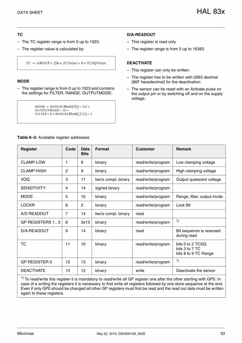
Table 6–3: Available register addresses
Register Code Data Bits
Format Customer Remark
CLAMP-LOW 1 8 binary read/write/program Low clamping voltage
CLAMP-HIGH 2 9 binary read/write/program High clamping voltage
VOQ 3 11 two’s compl. binary read/write/program Output quiescent voltage
SENSITIVITY 4 14 signed binary read/write/program
MODE 5 10 binary read/write/program Range, filter, output mode
LOCKR 6 2 binary read/write/program Lock Bit
A/D READOUT 7 14 two’s compl. binary read
GP REGISTERS 1...3 8 3x13 binary read/write/program 1)
D/A-READOUT 9 14 binary read Bit sequence is reversed during read
TC 11 10 binary read/write/program bits 0 to 2 TCSQbits 3 to 7 TCbits 8 to 9 TC Range
GP REGISTER 0 12 13 binary read/write/program 1)
DEACTIVATE 15 12 binary write Deactivate the sensor
1) To read/write this register it is mandatory to read/write all GP register one after the other starting with GP0. In case of a writing the registers it is necessary to first write all registers followed by one store sequence at the end. Even if only GP0 should be changed all other GP registers must first be read and the read out data must be written again to these registers.
HAL 83x DATA SHEET
34 May 22, 2015; DSH000169_002E Micronas
6.6. Programming Information
If the content of any register (except the lock registers)is to be changed, the desired value must first be writ-ten into the corresponding RAM register. Before read-ing out the RAM register again, the register value mustbe permanently stored in the EEPROM.
Permanently storing a value in the EEPROM is doneby first sending an ERASE command followed bysending a PROM command. The address within theERASE and PROM commands must be zero.ERASE and PROM act on all registers in parallel.
If all HAL83x registers are to be changed, all writingcommands can be sent one after the other, followed bysending one ERASE and PROM command at the end.
During all communication sequences, the customerhas to check if the communication with the sensor wassuccessful. This means that the acknowledge and theparity bits sent by the sensor have to be checked by
the customer. If the Micronas programmer board isused, the customer has to check the error flags sentfrom the programmer board.
Note: For production and qualification tests it is man-datory to set the LOCK bit after final adjustmentand programming of HAL83x. The LOCK func-tion is active after the next power-up of the sen-sor. The success of the lock process must bechecked by reading at least one sensor registerafter locking and/or by an analog check of thesensors output signal.Electrostatic discharges (ESD) may disturb theprogramming pulses. Please take precautionsagainst ESD.
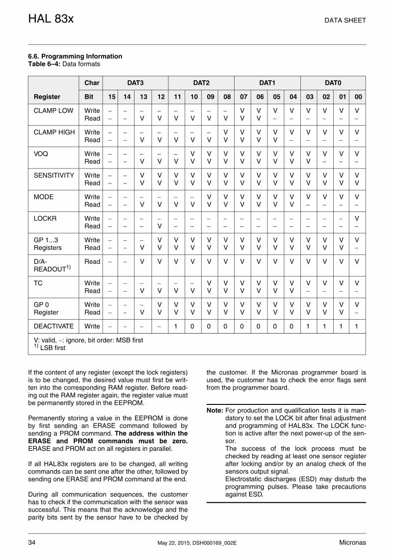
Table 6–4: Data formats
Register
Char DAT3 DAT2 DAT1 DAT0
Bit 15 14 13 12 11 10 09 08 07 06 05 04 03 02 01 00
CLAMP LOW WriteRead
V
V
V
V
V
V
VV
VV
V
V
V
V
V
V
CLAMP HIGH WriteRead
V
V
V
V
V
VV
VV
VV
VV
V
V
V
V
V
VOQ WriteRead
V
V
V
VV
VV
VV
VV
VV
VV
VV
VV
V
V
V
SENSITIVITY WriteRead
VV
VV
VV
VV
VV
VV
VV
VV
VV
VV
VV
VV
VV
VV
MODE WriteRead
V
V
V
V
VV
VV
VV
VV
VV
VV
V
V
V
V
LOCKR WriteRead
V
V
GP 1...3Registers
WriteRead
V
VV
VV
VV
VV
VV
VV
VV
VV
VV
VV
VV
VV
V
D/A-READOUT1)
Read V V V V V V V V V V V V V V
TC WriteRead
V
V
V
V
VV
VV
VV
VV
VV
VV
V
V
V
V
GP 0Register
WriteRead
V
VV
VV
VV
VV
VV
VV
VV
VV
VV
VV
VV
VV
V
DEACTIVATE Write 1 0 0 0 0 0 0 0 1 1 1 1
V: valid, : ignore, bit order: MSB first1) LSB first
HAL 83x DATA SHEET
35 May 22, 2015; DSH000169_002E Micronas
Micronas GmbHHans-Bunte-Strasse 19 D-79108 Freiburg P.O. Box 840 D-79008 Freiburg, Germany
Tel. +49-761-517-0 Fax +49-761-517-2174 E-mail: [email protected] Internet: www.micronas.com
7. Data Sheet History
1. Advance Information: ”HAL 83x Robust Mutlti-Pur-pose Programmable Linear Hall-Effect Sensor Fam-ily”, Jan. 13, 2013, AI000169_001EN. First release of the Advance Information.
2. Preliminary Data Sheet: “HAL 83x Robust Multi-Pur-pose Programmable Linear Hall-Effect Sensor Fam-ily”, Aug. 2, 2013, PD000213_001EN. First release of the preliminary data sheet. Major Changes:
– Absolute Maximum Ratings: Values for VESD
– Characteristics: Values for VOffset
3. Preliminary Data Sheet: “HAL 83x Robust Multi-Pur-pose Programmable Linear Hall-Effect Sensor Fam-ily”, Oct. 2, 2014, PD000213_002EN. Second release of the preliminary data sheet.Major Changes:
– TO92 UT package drawing updated
– TO92 UT package spread legs option deleted
– Recommended operating conditions and charac-teristics:
• Updated DNL value for HAL 835
• Updated RLmin (load resistor)
– Diagnostics and safety features updated
– Offset correction feature for HAL 835 removed
4. Data Sheet: “HAL 83x Robust Multi-Purpose Pro-grammable Linear Hall-Effect Sensor Family”, Feb. 25, 2015, DSH000169_001E. First release of the data sheet. Major Changes:
– Step Response Times
5. Data Sheet: “HAL 83x Robust Multi-Purpose Pro-grammable Linear Hall-Effect Sensor Family”, May 22, 2015, DSH000169_002E. Second release of the data sheet. Changes:
– Package TO92UT-1 (spread) added
– Package drawing TO92UT-2 (non-spread) updated
– Ammopack drawings updated
– Assembly and storage information
– Several text corrections
Mouser Electronics
Authorized Distributor
Click to View Pricing, Inventory, Delivery & Lifecycle Information: Micronas:
HAL830UT-A HAL835UT-A