Embed Size (px)
Citation preview
Chapter 3
Growth Structure and Device
Processing of DQW InGaAs/GaAs
Laser Diode
64
3. Growth Structure and Device Processing of DQW InGaAs/GaAs
Laser Diode
Fabrication of high-power laser diode requires a multilayered structure of semiconductor
materials having excellent electrical and optical quality, which is realized by the epitaxial
growth. A series of processing steps are required for the fabrication of laser diode bars
and devices out of the epitaxially grown laser diode structures. Post-growth processing is
a crucial issue for device fabrication and demands very careful optimization, since
threshold current and external efficiency depend on internal structures and the device
processing of laser diode. This chapter presents a brief report on the laser diode
structure and the processing steps used for the fabrication of edge-emitting high-power
laser diodes.
3.1 Introduction
Laser diodes have been realized over a wide range of lasing wavelength with a variety of
material systems. Since the first demonstration of the GaAs based homojunction laser
diode in 1962 [73], the threshold current densities have been brought down by more than
three orders of magnitude due to the advancement in the crystal growth technologies. In
the early 1970’s, improvements in Liquid Phase Epitaxy (LPE) enabled the realization of
the double heterostructure (DH) and continuous-wave (CW) operation of the laser diode
at room temperature [12]. Further, the development of quantum-well (QW) and quantum-
dot (QD) lasers, which are essential for realizing high-power laser diodes today, is
possible due to the advancement in molecular-beam epitaxy (MBE) and metalorganic
vapor phase epitaxy (MOVPE).
Most high-power laser diodes are based on III-V semiconductor QW structure
having an active layer thickness of about a few nanometers, which consists of precisely
controlled composition and good homogeneity throughout a wafer. The photon, generated
by the band-to-band recombination in the QW active region, is vertically (transversely)
confined by means of the waveguide layer comprising of the cladding and confinement
layer. The waveguide layers are much thicker, having thickness of 3-5 µm, and in order to
assure the economic feasibility of the process they have to be grown at a reasonable
65
growth rate. All of these have to be achieved while maintaining high crystalline quality
with minimal defects, with a tight control of the doping profile, and requiring optimized
epitaxial growth conditions for the individual layers of the laser structure. On the other
hand, lateral optical confinement is usually achieved by various post-growth processing
steps that define the laser device geometry viz. gain-guiding or index-guiding.
3.2 Epitaxial Growth of Semiconductor Materials
A lattice matched single crystal layer with controlled thickness and doping can be
achieved by means of an epitaxial growth process. The identical crystalline symmetry
between the substrate and the epitaxial layer is crucial for good quality epitaxial growth
of the layers. Selection of epi-layer composition to achieve lattice-matching, while
providing good carrier and optical confinement, is particularly important for the
heterostructures used in laser diodes. The lattice mismatch, i.e. the difference between the
lattice constants of the substrate and the epitaxial layer, should not exceed a critical limit.
The large value of lattice mismatch usually results in the generation of dislocations and
defects, degrading the quality of the grown layer. The lattice-mismatch also determines
the onset of three-dimensional (3D) growth-mode, commonly known as the Stranski-
Krastanov growth-mode [74].
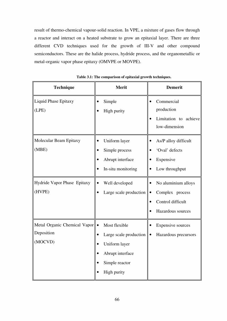
3.3 Epitaxial Growth Techniques
There are several epitaxial growth techniques viz. liquid phase epitaxy (LPE), molecular
beam epitaxy (MBE) and vapor phase epitaxy (VPE), of III-V compound semiconductor
materials and their heterostructures. Table 3.1 shows a comparative of various merits and
demerits of aforementioned epitaxial growth techniques [75].
3.3.1 Vapor Phase Epitaxy (VPE)
Vapor phase epitaxy (VPE), also known as chemical vapor deposition (CVD), refers to
the formation of a thin film on a crystalline substrate from a gaseous medium of different
chemical composition. Unlike physical vapor deposition (PVD), where condensation
occurs in the absence of a chemical change, the thin film growth takes place in VPE as a
66
result of thermo-chemical vapour-solid reaction. In VPE, a mixture of gases flow through
a reactor and interact on a heated substrate to grow an epitaxial layer. There are three
different CVD techniques used for the growth of III-V and other compound
semiconductors. These are the halide process, hydride process, and the organometallic or
metal-organic vapor phase epitaxy (OMVPE or MOVPE).
Table 3.1: The comparison of epitaxial growth techniques.
Technique Merit Demerit
Liquid Phase Epitaxy
(LPE)
• Simple
• High purity
• Commercial
production
• Limitation to achieve
low-dimension
Molecular Beam Epitaxy
(MBE)
• Uniform layer
• Simple process
• Abrupt interface
• In-situ monitoring
• As/P alloy difficult
• ‘Oval’ defects
• Expensive
• Low throughput
Hydride Vapor Phase Epitaxy
(HVPE)
• Well developed
• Large scale production
• No aluminium alloys
• Complex process
• Control difficult
• Hazardous sources
Metal Organic Chemical Vapor
Deposition
(MOCVD)
• Most flexible
• Large scale production
• Uniform layer
• Abrupt interface
• Simple reactor
• High purity
• Expensive sources
• Hazardous precursors
67
� Metal-Organic Vapor Phase Epitaxy (MOVPE)
Metal-organic vapour phase epitaxy (MOVPE), also known as organometallic vapour
phase epitaxy (OMVPE) or metal-organic chemical vapour deposition (MOCVD) is an
improvised form of VPE technique where the growth is carried out from the vapor phase
using organometallic and hydride sources [76]. It was first developed extensively by
Manasevit in 1968 for the growth of a variety of materials including III-V semiconductors
[77]. Since then, it has been advancing as a significant technique for the growth of high-
quality low- dimensional structure for fundamental semiconductor physics and for
semiconductor photonic devices such as single layers, heterojunctions, and QW structures
with excellent control over layer thickness, doping, and formation of hyper-abrupt isotype
and anisotype junctions. It was the MOVPE technique, which led to the room-
temperature operation of QW lasers for the first time [78] by means of the high-quality
epitaxial layer structures.
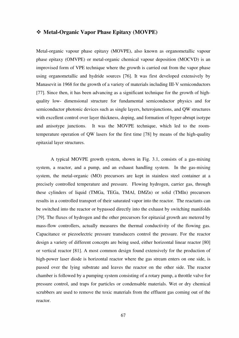
A typical MOVPE growth system, shown in Fig. 3.1, consists of a gas-mixing
system, a reactor, and a pump, and an exhaust handling system. In the gas-mixing
system, the metal-organic (MO) precursors are kept in stainless steel container at a
precisely controlled temperature and pressure. Flowing hydrogen, carrier gas, through
these cylinders of liquid (TMGa, TEGa, TMAl, DMZn) or solid (TMIn) precursors
results in a controlled transport of their saturated vapor into the reactor. The reactants can
be switched into the reactor or bypassed directly into the exhaust by switching manifolds
[79]. The fluxes of hydrogen and the other precursors for epitaxial growth are metered by
mass-flow controllers, actually measures the thermal conductivity of the flowing gas.
Capacitance or piezoelectric pressure transducers control the pressure. For the reactor
design a variety of different concepts are being used, either horizontal linear reactor [80]
or vertical reactor [81]. A most common design found extensively for the production of
high-power laser diode is horizontal reactor where the gas stream enters on one side, is
passed over the lying substrate and leaves the reactor on the other side. The reactor
chamber is followed by a pumping system consisting of a rotary pump, a throttle valve for
pressure control, and traps for particles or condensable materials. Wet or dry chemical
scrubbers are used to remove the toxic materials from the effluent gas coming out of the
reactor.
68
Figure 3.1: A typical MOVPE growth system.
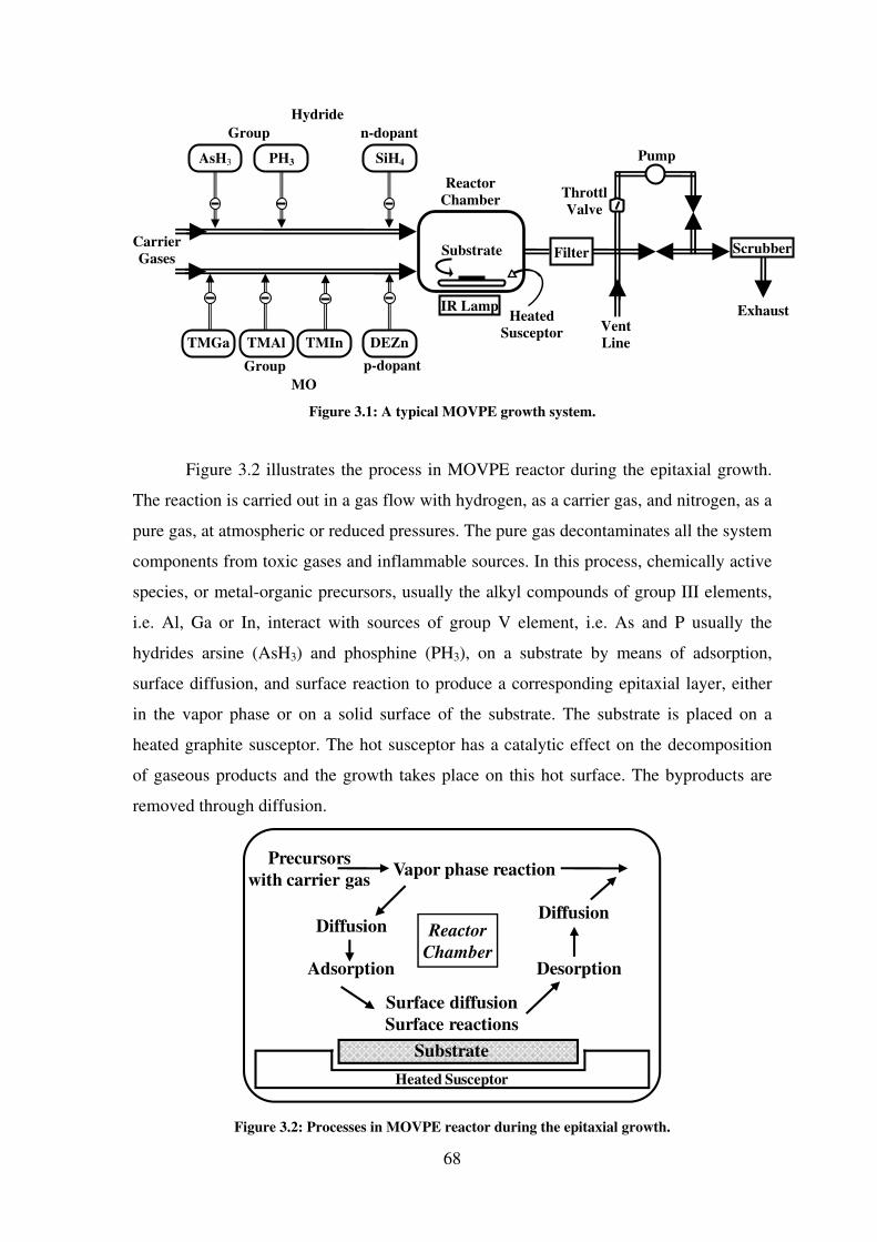
Figure 3.2 illustrates the process in MOVPE reactor during the epitaxial growth.
The reaction is carried out in a gas flow with hydrogen, as a carrier gas, and nitrogen, as a
pure gas, at atmospheric or reduced pressures. The pure gas decontaminates all the system
components from toxic gases and inflammable sources. In this process, chemically active
species, or metal-organic precursors, usually the alkyl compounds of group III elements,
i.e. Al, Ga or In, interact with sources of group V element, i.e. As and P usually the
hydrides arsine (AsH3) and phosphine (PH3), on a substrate by means of adsorption,
surface diffusion, and surface reaction to produce a corresponding epitaxial layer, either
in the vapor phase or on a solid surface of the substrate. The substrate is placed on a
heated graphite susceptor. The hot susceptor has a catalytic effect on the decomposition
of gaseous products and the growth takes place on this hot surface. The byproducts are
removed through diffusion.
Precursors
with carrier gas
Surface diffusion
Surface reactions
Adsorption Desorption
DiffusionDiffusion
Vapor phase reaction
Reactor
Chamber
Heated Susceptor
Substrate
Figure 3.2: Processes in MOVPE reactor during the epitaxial growth.
AsH3 PH3 SiH4
TMGa TMAl TMIn DEZn
IR Lamp
Substrate
Reactor
Chamber
Hydride
Group n-dopant
p-dopant Group
MO
Carrier
Gases Filter
Vent
Line
Scrubber
Throttl
Valve
Pump
Exhaust Heated
Susceptor
69
In MOVPE growth process, the basic chemical reaction is irreversible pyrolysis
that takes place in the vapor phase of a volatile metal-organic compound and a gaseous
hydride, and forming some intermediate compounds, given by, Eq. 3.1 [76]
n nR A DH AD nRH+ → + (3.1)
where, Rn indicates a lower order organic radical, such as a methyl- or ethyl-radical; A
and D are, the group III and V constituent species for the deposited solid, respectively.
An important example of this case is given by, Eq. 3.2,
( )600 C
3 3 433CH Ga AsH GaAs CH
°+ → + (3.2)
Finally, the constituent elements are released and get incorporated into the lattice on the
semiconductor surface.
The growth rate is one of the main parameters to be controlled during epitaxial
process, and is mainly decided by the growth temperature. The kinetics and
thermodynamics of the growth process play an important role, which defines the growth
rate and determines the driving force for the overall growth process, respectively. If the
reaction rate limits the growth rate, it is called kinetically limited case wherein the growth
rate increases with increase in temperature. Moreover, the processes like diffusion, called
mass transport, too, limit the growth rate, which is inversely proportional to pressure and
is independent of temperature. Growth rate is usually controlled by reaction kinetics in
low-temperature range and by mass transport in high-temperature range. The growth rate
is given as rg = (const.) pTMGa(V/P)1/2
for the growth process of GaAs, as in Eq. 3.2,
where, pTMGa = partial pressure of TMGa, V = gas velocity, P = reactor pressure.
A number of important and beneficial features are offered by the MOVPE growth
technique. Compounds, such as GaAs, can be grown with different As to Ga ratio (V/III
ratio) simply by varying the relative vapor pressure of arsine hydride (AsH3) and
trimethyl gallium (TMGa) as there is no need of establishing equilibrium with source
materials. This allows the study of native defects and trap states, which are supposed to
be related to the stoichiometry. It is possible to grow almost all the III-V semiconductor
compounds, their ternary and quaternary alloys, using MOVPE. Growth of high purity,
ultra-thin layers, and abrupt junctions with precise composition and doping control makes
this technique more prevalent in the field of optoelectronic device fabrication.
70
3.3.2 Materials for High-Power Laser Diodes
The direct energy bandgap and lattice constant of the material are the most crucial
parameters in the material selection for laser diodes. Hence, the elementary
semiconductors e.g. silicon or germanium are not used for lasers because of their indirect
energy bandgap. The III-V compound semiconductor materials are widely used for the
fabrication of high-power laser diodes. The III-V binary compounds are formed by
combining elements form group III and group V of the periodic table while, ternary or
quaternary compounds are formed through alloyed binary compounds. The energy
bandgap and the lattice constant of ternary and quaternary compounds depend on the
mole fraction of the constituent binary compounds. For example, the lattice constant of
any ternary compound (AxB1-xC) is calculated with the help of Vegard’s law [82] using
Eq. 3.3.
1(1 )
x xA B C AC BCa xa x a−
= + − (3.3)
where, AC and BC are binary compounds such as InP, GaP. Similarly, the energy
bandgap of any ternary compound (AxB1-xC) can be calculated as,
1)1()1(1
CxxEgxxEgEg BCACCBA xx−+−+=
− (3.4)
where, C1 is the Bowing parameter of ternary material [83].
As the alloy composition changes the band structure and hence electronic and
optical properties of the alloy changes. Thus by choosing appropriate compounds or
alloys, it is possible to select and tune the emission wavelengths for laser diodes. The
choice of material system for the fabrication of laser diode is determined by the emission
wavelength (λ) of interest and hence by the energy bandgap (Eg) of the active region in
the laser structure as,
(eV)(nm)
g
hc 1239E = =
λ λ (3.5)
where, h is Plank’s constant and c is velocity of light. Therefore, the lasers having
wavelength in the range of 600-700 nm can be assessed using ternary or quaternary
compound viz. AlGaAs, InGaP, AlGaInP. Also, lattice matched AlGaAs grown on GaAs
can realize laser emission wavelength in the range 700-870 nm, whereas using
InGaAs/GaAs strained quantum well system the wavelength range can be extended
71
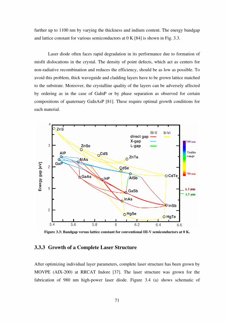
further up to 1100 nm by varying the thickness and indium content. The energy bandgap
and lattice constant for various semiconductors at 0 K [84] is shown in Fig. 3.3.
Laser diode often faces rapid degradation in its performance due to formation of
misfit dislocations in the crystal. The density of point defects, which act as centers for
non-radiative recombination and reduces the efficiency, should be as low as possible. To
avoid this problem, thick waveguide and cladding layers have to be grown lattice matched
to the substrate. Moreover, the crystalline quality of the layers can be adversely affected
by ordering as in the case of GaInP or by phase separation as observed for certain
compositions of quaternary GaInAsP [81]. These require optimal growth conditions for
each material.
Figure 3.3: Bandgap versus lattice constant for conventional III-V semiconductors at 0 K.
3.3.3 Growth of a Complete Laser Structure
After optimizing individual layer parameters, complete laser structure has been grown by
MOVPE (AIX-200) at RRCAT Indore [37]. The laser structure was grown for the
fabrication of 980 nm high-power laser diode. Figure 3.4 (a) shows schematic of
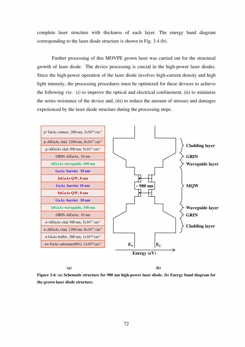
72
complete laser structure with thickness of each layer. The energy band diagram
corresponding to the laser diode structure is shown in Fig. 3.4 (b).
Further processing of this MOVPE grown laser was carried out for the structural
growth of laser diode. The device processing is crucial in the high-power laser diodes.
Since the high-power operation of the laser diode involves high-current density and high
light intensity, the processing procedures must be optimized for these devices to achieve
the following viz. (i) to improve the optical and electrical confinement, (ii) to minimize
the series resistance of the device and, (iii) to reduce the amount of stresses and damages
experienced by the laser diode structure during the processing steps.
p+ GaAs contact, 200 nm, 2x1019 cm-3
p-AlGaAs clad, 1200 nm, 8x1017 cm-3
p-AlGaAs clad 300 nm, 5x1017 cm-3
GRIN-AlGaAs, 10 nm
AlGaAs waveguide, 100 nm
GaAs barrier 10 nm
InGaAs QW, 8 nm
GaAs barrier 10 nm
InGaAs QW, 8 nm
GaAs barrier 10 nm
AlGaAs waveguide, 100 nm
GRIN-AlGaAs, 10 nm
n-AlGaAs clad 300 nm, 5x1017 cm-3
n-AlGaAs clad, 1200 nm, 8x1017 cm-3
n-GaAs buffer, 200 nm, 1x1018 cm-3
n+-GaAs substrate(001), 1x1018 cm-3
Energy (eV)
~ 980 nm
Cladding layer
Cladding layer
Waveguide layer
GRIN
GRIN
MQW
EV EC
Waveguide layer
(a) (b)
Figure 3.4: (a) Schematic structure for 980 nm high-power laser diode. (b) Energy band diagram for
the grown laser diode structure.
73
3.4 Various Laser Diode Geometries
The edge emitting laser diodes are fabricated mainly in two device geometries. These are
broad-area geometry and stripe geometry.
3.4.1 Broad-Area Laser Diodes
The broad-area laser diodes are the most elementary form of edge-emitting laser diodes.
In these lasers, the stripe-width is much larger than the thickness of the laser structure,
which allows uniform distribution of the injected current and the optical field in lateral
direction. Nevertheless, due to large lateral dimensions many transverse modes can
sustain this type of laser structure. Moreover, the filamentation, i.e. lateral beam
distortions due to increase in refractive index, in broad-area devices is very well-known,
and limits the high-power operation of the device.
3.4.2 Stripe Geometry Laser Diodes
As the name suggests, laser diodes with a few µm wide narrow stripe for lateral current
confinement are known as stripe geometry injection lasers. This current confinement into
the device can effectively overcome the issues like filamentation. The stripe geometry
laser diodes can again be categorized into gain-guided, index-guided and buried
heterostructures, according to different types of lateral confinement mechanisms viz.
current, optical or photon, and carrier confinement, respectively.
Laser diodes, which only have current confinement, are called gain-guided lasers.
In case of gain-guided lasers the lateral wave-guide is defined simply by the contact
geometry. The current confinement is provided by an aperture, which is mostly realized
by a dielectric isolator as shown in Fig. 3.5 (a). Though the fabrication of this laser is
easy, there are some disadvantages as well. The threshold current in this devices is high
compared to the index-guided one because of optical loss in waveguide.
The waveguiding in index-guided laser diode is achieved by means of lateral
effective refractive index step difference formed by a very small mesa-structure in the
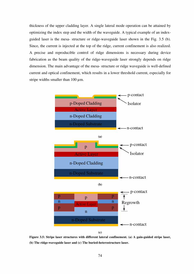
74
thickness of the upper cladding layer. A single lateral mode operation can be attained by
optimizing the index step and the width of the waveguide. A typical example of an index-
guided laser is the mesa- structure or ridge-waveguide laser shown in the Fig. 3.5 (b).
Since, the current is injected at the top of the ridge, current confinement is also realized.
A precise and reproducible control of ridge dimensions is necessary during device
fabrication as the beam quality of the ridge-waveguide laser strongly depends on ridge
dimension. The main advantage of the mesa- structure or ridge waveguide is well-defined
current and optical confinement, which results in a lower threshold current, especially for
stripe widths smaller than 100 µm.
p-Doped Cladding
p-contact
n-Doped Cladding
Active Layer
n-Doped Substraten-contact
Isolator
(a)
p-contact
n-Doped Cladding
Active Layer
n-Doped Substraten-contact
Isolator
p
(b)
p
p-contact
n-contact
n
n-Doped Substrate
Active Layer Regrowth
p
p
n
p
p
n
(c)
Figure 3.5: Stripe laser structures with different lateral confinement. (a) A gain-guided stripe laser,
(b) The ridge-waveguide laser and (c) The buried-heterostructure laser.
75
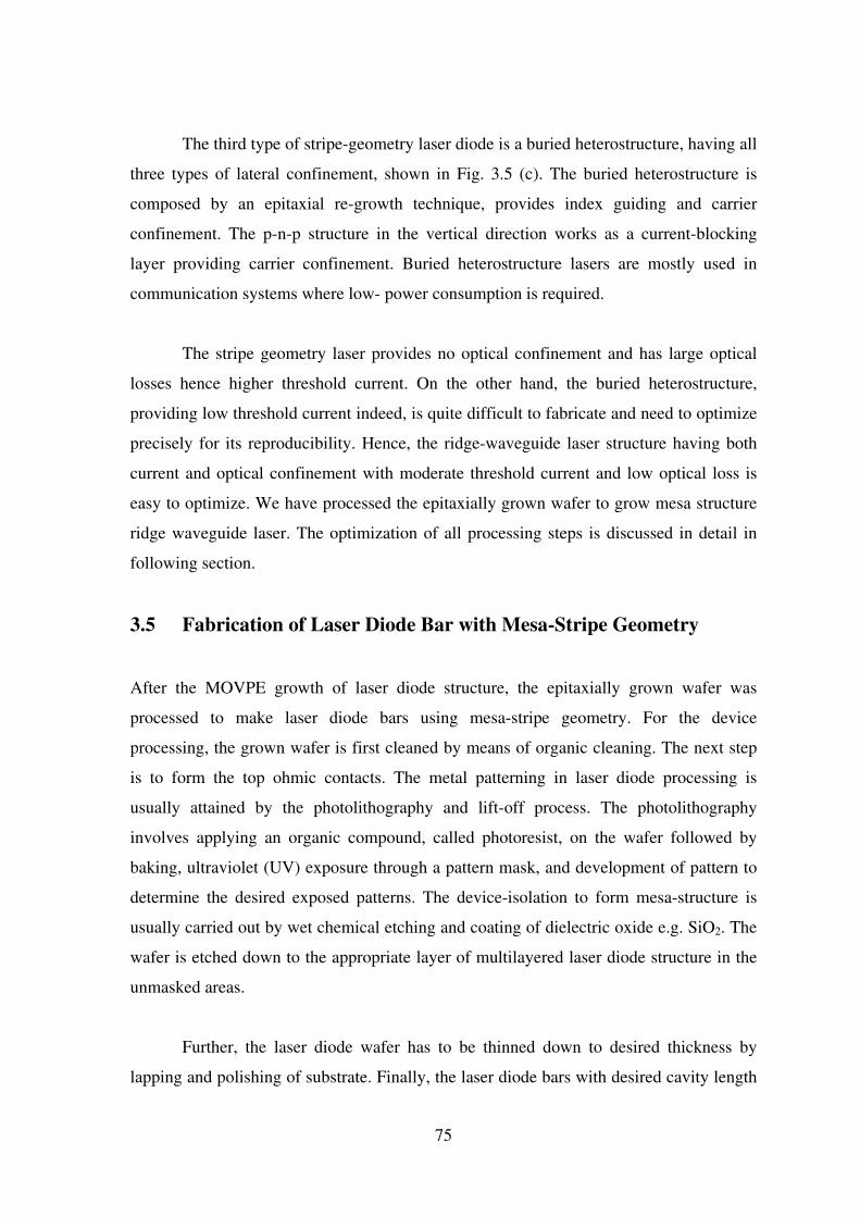
The third type of stripe-geometry laser diode is a buried heterostructure, having all
three types of lateral confinement, shown in Fig. 3.5 (c). The buried heterostructure is
composed by an epitaxial re-growth technique, provides index guiding and carrier
confinement. The p-n-p structure in the vertical direction works as a current-blocking
layer providing carrier confinement. Buried heterostructure lasers are mostly used in
communication systems where low- power consumption is required.
The stripe geometry laser provides no optical confinement and has large optical
losses hence higher threshold current. On the other hand, the buried heterostructure,
providing low threshold current indeed, is quite difficult to fabricate and need to optimize
precisely for its reproducibility. Hence, the ridge-waveguide laser structure having both
current and optical confinement with moderate threshold current and low optical loss is
easy to optimize. We have processed the epitaxially grown wafer to grow mesa structure
ridge waveguide laser. The optimization of all processing steps is discussed in detail in
following section.
3.5 Fabrication of Laser Diode Bar with Mesa-Stripe Geometry
After the MOVPE growth of laser diode structure, the epitaxially grown wafer was
processed to make laser diode bars using mesa-stripe geometry. For the device
processing, the grown wafer is first cleaned by means of organic cleaning. The next step
is to form the top ohmic contacts. The metal patterning in laser diode processing is
usually attained by the photolithography and lift-off process. The photolithography
involves applying an organic compound, called photoresist, on the wafer followed by
baking, ultraviolet (UV) exposure through a pattern mask, and development of pattern to
determine the desired exposed patterns. The device-isolation to form mesa-structure is
usually carried out by wet chemical etching and coating of dielectric oxide e.g. SiO2. The
wafer is etched down to the appropriate layer of multilayered laser diode structure in the
unmasked areas.
Further, the laser diode wafer has to be thinned down to desired thickness by
lapping and polishing of substrate. Finally, the laser diode bars with desired cavity length
76
are scribed and cleaved. The processing is generally carried out in the class-10,000 clean-
room, i.e., the room contains less than 10,000 particles of size more than 0.5 µm in a
cubic foot of air. All these steps for fabrication of laser diode bars with mesa stripe
geometry and their optimization for our structure is discussed in the next section in their
processing sequence.
3.6 Optimization of Various Steps in Laser Diode Processing
The post-growth device processing of laser diodes were carried out at Semiconductor
Laser Section, SSLD, RRCAT, Indore. The wafers were first cleaved into small pieces of
about 1 inch area. Here, it is important to identify the crystalline direction lying within the
surface plane since the etching profile is good in the primary flat direction and it is easy
to cleave the sample in the direction perpendicular to the primary flat in order to obtain
the cavity mirrors.
3.6.1 Organic Cleaning
The organic cleaning is preliminary practice to clean the semiconductor wafer from
various contaminants e.g. dust, greases and other oily impurities. The sample was first
cleaned in warm trichloroethylene (TCE) which removes oily impurities from the sample.
Furthermore, the sample was cleaned in acetone and methanol, respectively, to remove
the effect of previously used chemical, i.e. acetone to remove TCE and methanol for
acetone. Finally, the sample was cleaned by de-ionized (DI) water. These organic
solvents are effective in removing oils, greases, waxes and organic materials such as
photoresists from the sample surface. The sample was then dried under nitrogen flow, and
made ready for photolithography, which defines the transverse dimension of laser diode.
3.6.2 Photolithography
Photolithography is a process to form desired pattern on semiconductor surface by means
of pattern-masking on an intermediate photosensitive polymer film called photoresist.
The semiconductor surface, coated with photoresist, is then exposed through mask and
developed to realize desired pattern by removing excess photoresist. The remaining
77
pattern can then be replicated in other materials in subsequent processing, using
techniques such as etching, metallization, etc. The resolution is limited by the diffraction
effect, which increases with the square root of the wavelength and with the gap between
the mask and the wafer [85]. Various steps involved in photolithography are given below.
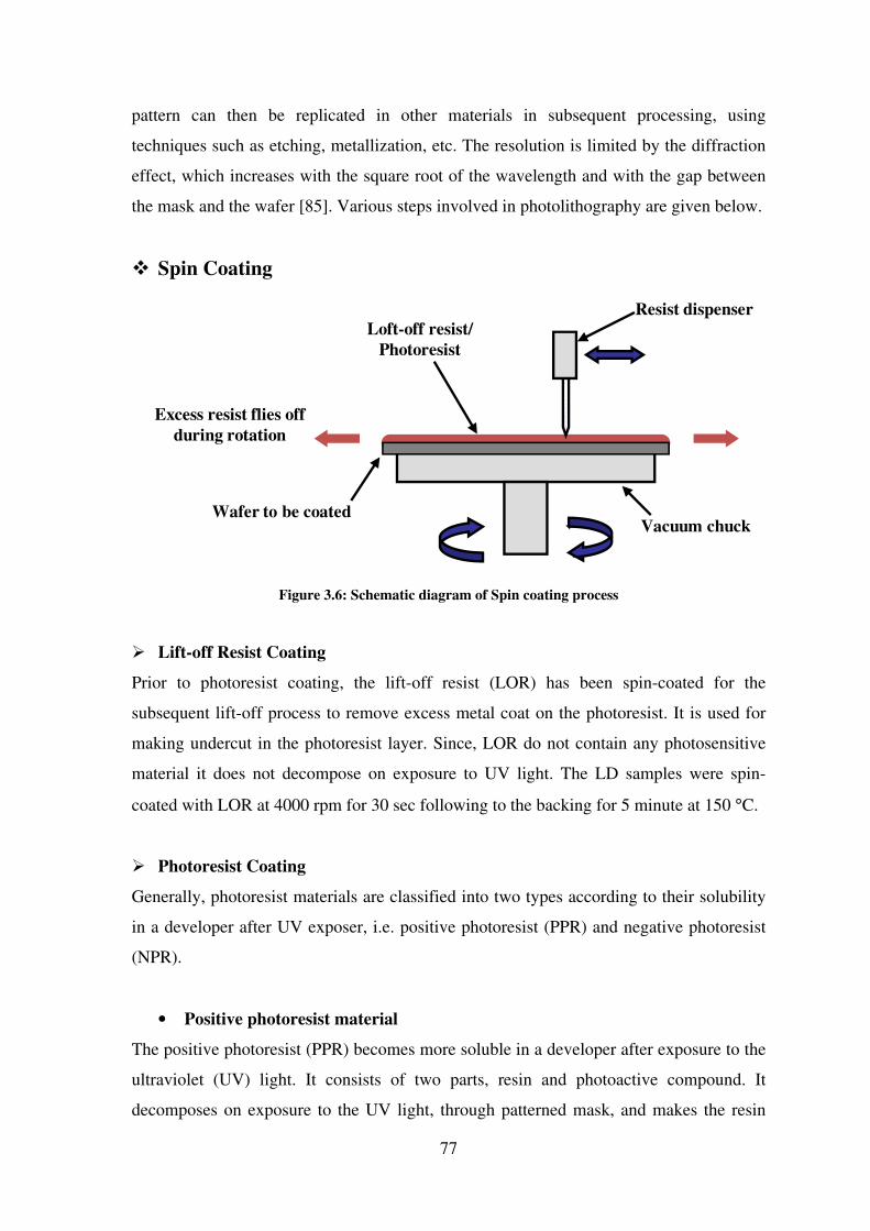
� Spin Coating
Vacuum chuck
Loft-off resist/
Photoresist
Wafer to be coated
Excess resist flies off
during rotation
Resist dispenser
Figure 3.6: Schematic diagram of Spin coating process
� Lift-off Resist Coating
Prior to photoresist coating, the lift-off resist (LOR) has been spin-coated for the
subsequent lift-off process to remove excess metal coat on the photoresist. It is used for
making undercut in the photoresist layer. Since, LOR do not contain any photosensitive
material it does not decompose on exposure to UV light. The LD samples were spin-
coated with LOR at 4000 rpm for 30 sec following to the backing for 5 minute at 150 °C.
� Photoresist Coating
Generally, photoresist materials are classified into two types according to their solubility
in a developer after UV exposer, i.e. positive photoresist (PPR) and negative photoresist
(NPR).
• Positive photoresist material
The positive photoresist (PPR) becomes more soluble in a developer after exposure to the
ultraviolet (UV) light. It consists of two parts, resin and photoactive compound. It
decomposes on exposure to the UV light, through patterned mask, and makes the resin
78
more soluble in developer. Hence, the exposed resist is then washed away, leaving
windows of underlying material.
• Negative photoresist material
As the name suggest, the negative photoresist (NPR) behaves exactly opposite to the
PPR. It becomes less soluble in developer after exposure to the UV light. It consists of
chemical inert rubber and photoactive agent. Exposure to the UV light causes the negative
resist to become polymerized, and more difficult to dissolve in developer. Hence,
developer solution can only remove the unexposed photoresist. Masks used for NPR,
therefore, contain the inverse (or photographic "negative") of the pattern to be transferred.
Both PPR and NPR have their merits and demerits, listed in Table 3.2. We have
used PPR for lithography, as it provides good step coverage and dissolve in aqueous
developer. It is deposited on the semiconductor surface by means of spin coating.
Table 3.2: Differences between positive photoresist and negative photoresist.
NPR PPR
Swells during develop No swelling during develop
Marginal step coverage Good step coverage
Organic solvent developer Aqueous developer
Sensitive to O2 Operate well in air [86]
We used OiR-960 positive photoresist (S1813) for photolithography of laser diode
samples. The samples were coated with PPR, having thickness about 1 µm, at 3500 rpm
and soft baked at 95 °C on a hot plate for one minute.
� Alignment & Exposure
A photomask consists of desired pattern, i.e. alternate transparent and opaque stripes, to
realize laser diode mesa structure was aligned to the wafer. The photomask, having stripe
width 100 µm, used for patterning is shown in Fig. 3.7, having opaque Fe2O3/chromium
stripe pattern on a soda lime glass substrate.
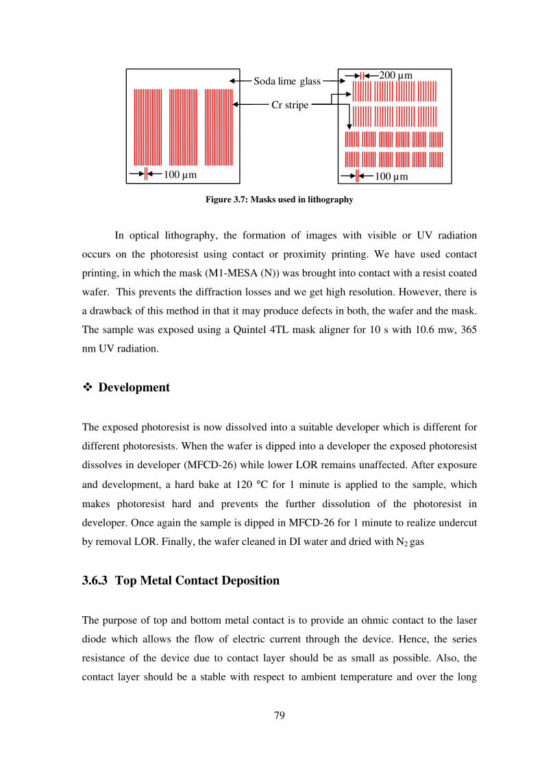
79
Soda lime glass
100 µm
Cr stripe
100 µm
200 µm
Figure 3.7: Masks used in lithography
In optical lithography, the formation of images with visible or UV radiation
occurs on the photoresist using contact or proximity printing. We have used contact
printing, in which the mask (M1-MESA (N)) was brought into contact with a resist coated
wafer. This prevents the diffraction losses and we get high resolution. However, there is
a drawback of this method in that it may produce defects in both, the wafer and the mask.
The sample was exposed using a Quintel 4TL mask aligner for 10 s with 10.6 mw, 365
nm UV radiation.
� Development
The exposed photoresist is now dissolved into a suitable developer which is different for
different photoresists. When the wafer is dipped into a developer the exposed photoresist
dissolves in developer (MFCD-26) while lower LOR remains unaffected. After exposure
and development, a hard bake at 120 °C for 1 minute is applied to the sample, which
makes photoresist hard and prevents the further dissolution of the photoresist in
developer. Once again the sample is dipped in MFCD-26 for 1 minute to realize undercut
by removal LOR. Finally, the wafer cleaned in DI water and dried with N2 gas
3.6.3 Top Metal Contact Deposition
The purpose of top and bottom metal contact is to provide an ohmic contact to the laser
diode which allows the flow of electric current through the device. Hence, the series
resistance of the device due to contact layer should be as small as possible. Also, the
contact layer should be a stable with respect to ambient temperature and over the long
80
period time. Therefore, low contact resistance, ease of fabrication, better adhesion, and
thermal stability are the primary quality requirements of the metal to realize a good
quality contact layer.
The metallization is also the basis for the laser diode mounting on a heat sink
which allows soldering, also known as die-bonding, and wire bonding. Generally, for
high-power diode lasers based on GaAs substrates, the semiconductor contact layer
consists typically of heavily doped p- and n-type GaAs. Almost any metal placed in
intimate contact with these heavily doped GaAs surface will result in an ohmic contact
without any alloy formation. We have deposited multilayer of Titanium (Ti) (~10 nm)/
Platinum (Pt) (~5 nm) / Gold (Au) (~200 nm) in sequence to deposit p-type ohmic
contacts. Here, Ti and Pt are used for the better adhesion of top Au layer, which provides
a very high conductivity and a soft surface quality for device bonding. The front contacts
to the p+ GaAs capping layer of the laser structures were deposited using a metal coating
unit with thermal evaporation system at high vacuum (3×10⁻⁶
mbar pressure)
3.6.4 Lift-off Process
Lift-off process is a simple method for patterning films which are deposited on the
sample. In this step, we remove the metallic layer from the top of mesas, by means of
warm (65 °C) PG remover bath. The PG remover reacts with LOR and causes swelling
and losing adhesion to the wafer and hence excess metal deposited on the photoresist is
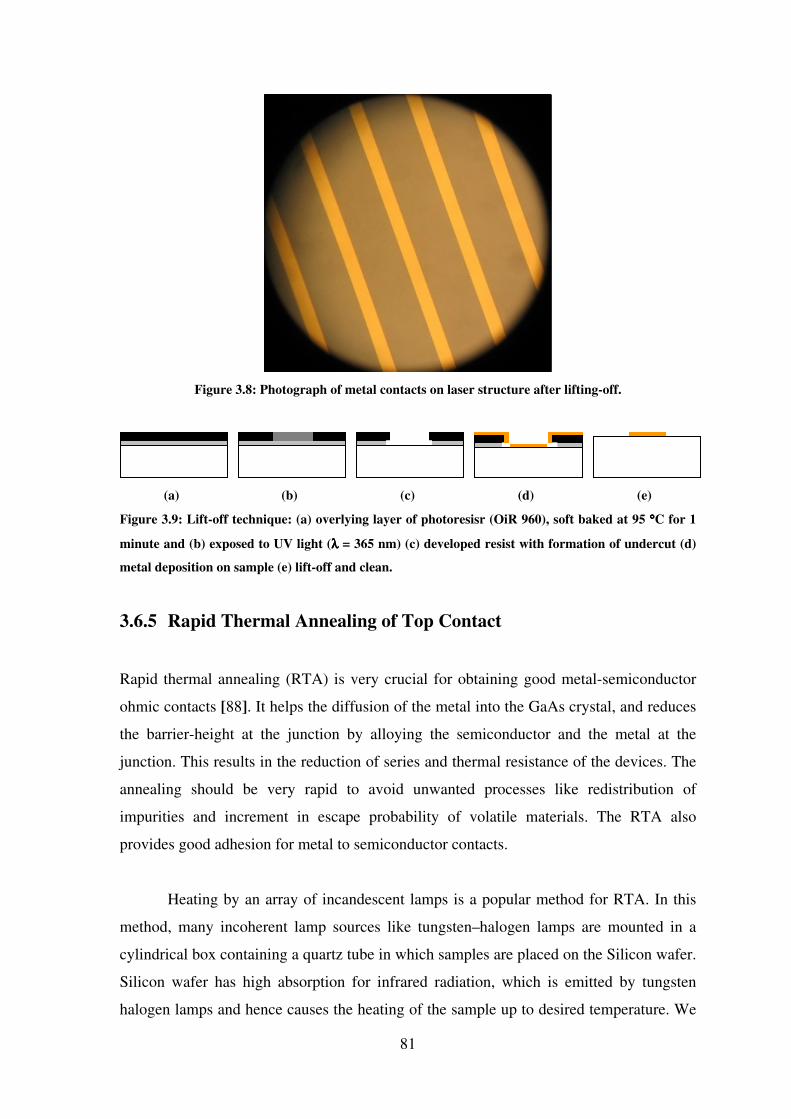
removed while metal directly deposited on wafer remains unchanged. Figure 3.8 shows
the final structure of the top p-contact surface.
Any deposited film can be lifted-off provided that the substrate does not reach the
temperature high enough to burn the photoresist during the deposition and the film is thin
enough to allow solvent to seep underneath. Various mechanisms from resist coat to lift
off are shown in Fig. 3.9 [87].
81
Figure 3.8: Photograph of metal contacts on laser structure after lifting-off.
(a) (b) (c) (d) (e)
Figure 3.9: Lift-off technique: (a) overlying layer of photoresisr (OiR 960), soft baked at 95 °°°°C for 1
minute and (b) exposed to UV light (λλλλ = 365 nm) (c) developed resist with formation of undercut (d)
metal deposition on sample (e) lift-off and clean.
3.6.5 Rapid Thermal Annealing of Top Contact
Rapid thermal annealing (RTA) is very crucial for obtaining good metal-semiconductor
ohmic contacts [88]. It helps the diffusion of the metal into the GaAs crystal, and reduces
the barrier-height at the junction by alloying the semiconductor and the metal at the
junction. This results in the reduction of series and thermal resistance of the devices. The
annealing should be very rapid to avoid unwanted processes like redistribution of
impurities and increment in escape probability of volatile materials. The RTA also
provides good adhesion for metal to semiconductor contacts.
Heating by an array of incandescent lamps is a popular method for RTA. In this
method, many incoherent lamp sources like tungsten–halogen lamps are mounted in a
cylindrical box containing a quartz tube in which samples are placed on the Silicon wafer.
Silicon wafer has high absorption for infrared radiation, which is emitted by tungsten
halogen lamps and hence causes the heating of the sample up to desired temperature. We
82
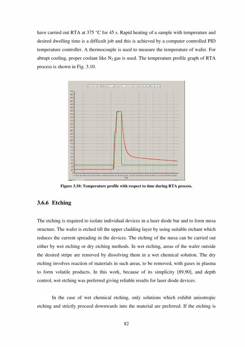
have carried out RTA at 375 °C for 45 s. Rapid heating of a sample with temperature and
desired dwelling time is a difficult job and this is achieved by a computer controlled PID
temperature controller. A thermocouple is used to measure the temperature of wafer. For
abrupt cooling, proper coolant like N2 gas is used. The temperature profile graph of RTA
process is shown in Fig. 3.10.
Figure 3.10: Temperature profile with respect to time during RTA process.
3.6.6 Etching
The etching is required to isolate individual devices in a laser diode bar and to form mesa
structure. The wafer is etched till the upper cladding layer by using suitable etchant which
reduces the current spreading in the devices. The etching of the mesa can be carried out
either by wet etching or dry etching methods. In wet etching, areas of the wafer outside
the desired stripe are removed by dissolving them in a wet chemical solution. The dry
etching involves reaction of materials in such areas, to be removed, with gases in plasma
to form volatile products. In this work, because of its simplicity [89,90], and depth
control, wet etching was preferred giving reliable results for laser diode devices.
In the case of wet chemical etching, only solutions which exhibit anisotropic
etching and strictly proceed downwards into the material are preferred. If the etching is
83
isotropic, a large undercut occurs resulting in breaks and degradation of metallization
films and the structure [85]. Though the wet etching forms an undercut and hard to
control it is mostly used due to its low cost, easy to implement, high etching rate, good
selectivity for most materials and produce better electronic properties.
The etching solution for GaAs and AlGaAs usually contain hydrogen peroxide
(H2O2), to oxidize the semiconductor surface, and phosphoric acid (H3PO4), to dissolve
the oxidized components of mixture. In the present study, H3PO4 etching solution has
been used. The H3PO4 / H2O2 / CH3OH system is used to etch GaAs and AlGaAs at
controlled rates. This is due to high viscosity of H3PO4, so that diffusion of the hydrogen
peroxide to the semiconductor surface becomes the rate - limiting step. In this study, a
mixture of CH3OH / H3PO4 / H2O2 in 6:3:1 ratio is made as an etching solution for GaAs
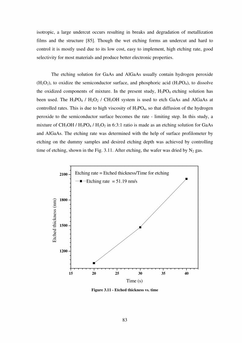
and AlGaAs. The etching rate was determined with the help of surface profilometer by
etching on the dummy samples and desired etching depth was achieved by controlling
time of etching, shown in the Fig. 3.11. After etching, the wafer was dried by N2 gas.
15 20 25 30 35 40
1200
1500
1800
2100
Etc
hed
thic
knes
s (n
m)
Time (s)
Etching rate = 51.19 nm/s
Etching rate = Etched thickness/Time for etching
Figure 3.11 - Etched thickness vs. time
84
3.6.7 SiO2 Deposition and Window Opening
For better isolation and surface state passivation of laser diode, dielectric layers are used
as a current barrier between isolated laser diodes after GaAs/AlGaAs etching. The oxide
deposition improves the performance of the laser diode because it isolates the devices
completely and prevents tunneling of carriers from one diode to other. So the carrier loss
is reduced and directly injected to the active region. Thus the injection efficiency of the
laser diode is also improved. We have deposited SiO2 dielectric layer of ~200 nm on
GaAs/AlGaAs etched mesa laser diode structure. After SiO2 deposition it is necessary to
remove the SiO2 from the top of metal contact region. To do so we have again used
photolithography and selective etching of SiO2 with following sequential process
execution.
• 200 nm thick SiO2 deposition on etched laser diode wafer.
• Spin coating of PPR for 30 s at 3500 rpm.
• Soft baking at 95 °C for 1 min.
• Mask alignment in such a way that only exposed PPR coated on metal stripe.
• Exposure to UV light for 10 s.
• Etching of selective SiO2 Buffer Hydro-Fluoric acid (BHF).
• Develop for 1 min with developer, to remove PPR from SiO2.
• Then clean with acetone, methanol, and DI water.
• Dry it with N2 gas.
To make the Buffer Hydro-Fluoric acid (BHF), 40 g of ammonium fluoride
(NH4F) is dissolved in 60 ml of DI water. The solution is then mixed with HF acid in a
ratio of 6:1. The overall chemical reaction for SiO2 etching is: SiO2 + 6HF → H2SiF6 +
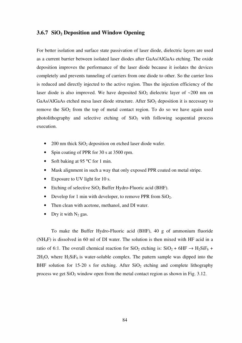
2H2O, where H2SiF6 is water-soluble complex. The pattern sample was dipped into the
BHF solution for 15-20 s for etching. After SiO2 etching and complete lithography
process we get SiO2 window open from the metal contact region as shown in Fig. 3.12.
85
Figure 3.12: Sample photograph after window opening by removal of SiO2 with BHF.
3.6.8 Lapping and Polishing
In order to reduce the thermal resistance of the device and to facilitate the scribing
procedure, it is necessary to thin down the wafer by reducing the substrate thickness. This
is accomplished by reducing the thickness of n+ GaAs wafer to around 150 µm by
mechanical lapping and polishing the wafer manually. Lapping was done using alumina
powder or diamond pest, having particle/grain size 5 µm and 1 µm, to reduce thickness
followed by polishing with alumina slurry, having particle size 0.5 µm, to mirror polished
the surface. Polishing is necessary to achieve uniform surface with minimum roughness
which reduces the device resistance and helps to get void-free die-bonding. After lapping
and polishing, the wafer was cleaned organically and the bottom surface of the wafer was
chemically polished by means of etching using CH3OH / H3PO4 / H2O2 etching solution.
Finally, the wafer was cleaned with DI water and dried under nitrogen flow.
3.6.9 Bottom Metal Contact Deposition
After the samples are thinned by lapping and polishing, it is necessary to cover this
surface entirely, for the n-contact of the laser devices. The most common approach of
fabricating ohmic contacts on n-GaAs is to apply an appropriate metallization to the
wafer, and then alloy the metal into the GaAs. During the alloying and cooling period, a
86
component of the metal enters into the GaAs and highly dopes the surface layer. This
doping decreases the Schottky barrier and the tunneling dominates the conduction
mechanism. The doping agent is generally chosen to be germanium (Ge). Gold-
germanium (Au-Ge) is usually applied with an overlay of another thin metal layer such as
nickel (Ni). Addition of Ni to Au-Ge leads to lower contact resistance as well as serving
to maintain a smooth surface morphology after alloying the contact metallization [91].
The Au-Ge alloy has a poor sheet resistance, is very difficult to wire-bond and is not
solderable to a heat sink. This requires an additional gold layer to be deposited on the Au-
Ge alloy. The sequence for bottom ohmic contact deposition on n-type substrate is Au-Ge
(~ 5 nm) /Ni (~ 5 nm) /Au (~ 100-200 nm). To achieve intimate contact formation
between GaAs substrate and the deposited metals, we have carried out RTA at 375 °C for
45 s.
3.6.10 Scribing
Finally, the wafer is cleaved along the cleavage plane, i.e. (110) for GaAs, perpendicular
to laser diode stripes using Micro Suss HR 100 manual scriber to get laser diode bars with
different cavity lengths ranging from 0.5 mm to 2 mm. Each bar contains several laser
diodes with stripe width of 100 µm.
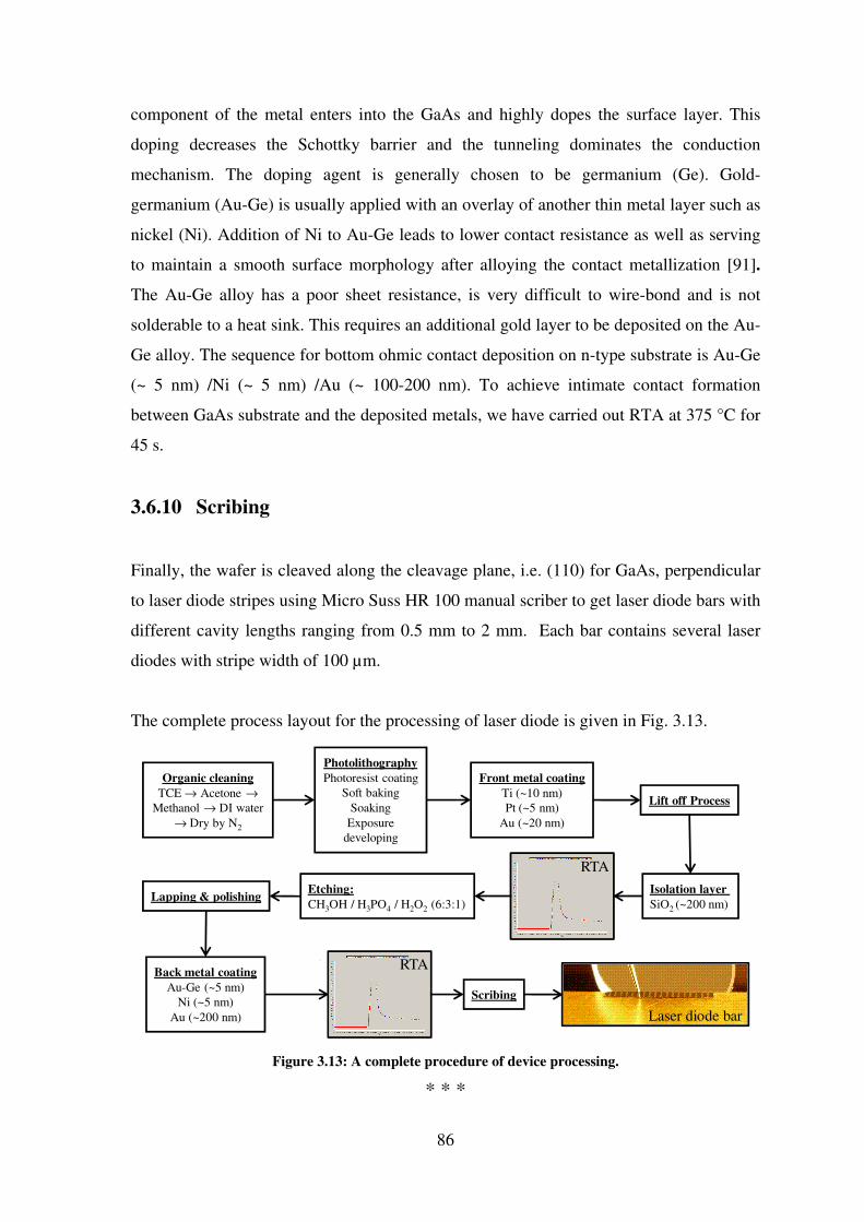
The complete process layout for the processing of laser diode is given in Fig. 3.13.
Front metal coating
Ti (~10 nm)
Pt (~5 nm)
Au (~20 nm)
Lift off Process
Etching:
CH3OH / H3PO4 / H2O2 (6:3:1)Lapping & polishing
Scribing
Photolithography
Photoresist coating
Soft baking
Soaking
Exposure
developing
Organic cleaning
TCE → Acetone →
Methanol → DI water
→ Dry by N2
Back metal coating
Au-Ge (~5 nm)
Ni (~5 nm)
Au (~200 nm)
Isolation layer
SiO2 (~200 nm)
RTA
RTA
Laser diode bar
Figure 3.13: A complete procedure of device processing.
* * *


![STATE OF VERMONT RETAINER CONTRACT FOR IT ......1 of 59 STATE OF VERMONT RETAINER CONTRACT FOR IT PROFESSIONAL SERVICES [CODE FOR AMERICA LABS INC. - CONTRACT # 38133] 1. Parties.This](https://img.pdfslide.us/doc/110x75/5f0cf5c67e708231d437fb64/state-of-vermont-retainer-contract-for-it-1-of-59-state-of-vermont-retainer.jpg)


![HUV +RXVWRQ $WDVK .DGHK RSHQLQJ ZZZ ]DQW RUJ =$17 … · 02-01-2019 · Member’s Name Age Range Children’s Name Age According to ZANT Bylaws, Regular & Life Membership is open](https://img.pdfslide.us/doc/110x75/5ec0dd445902095e567fd93d/huv-rxvwrq-wdvk-dghk-rshqlqj-zzz-dqw-ruj-17-02-01-2019-memberas-name.jpg)
![ENSURING A SOCIETY OF ALL AGES - Social Platform€¦ · iru uhjlrqdo frrshudwlrq lq wkh lpsohphqwdwlrq dqg prqlwrulqj ri 5,6 0,3$$ 09. :h duh frjql]dqw wkdw wkh dgydqfhphqw wrzdugv](https://img.pdfslide.us/doc/110x75/5fc2260abe989200103d6a5c/ensuring-a-society-of-all-ages-social-iru-uhjlrqdo-frrshudwlrq-lq-wkh-lpsohphqwdwlrq.jpg)

![HOM Coupler Alterations for the LHC DQW Crab Cavity[3] B. Muratoriand T. Pieloni, “Luminosity Levelling techniques for the LHC", (CERN, Geneva, Switzerland), pp. 177–181, Proceedings,](https://img.pdfslide.us/doc/110x75/5f1088927e708231d4499462/hom-coupler-alterations-for-the-lhc-dqw-crab-cavity-3-b-muratoriand-t-pieloni.jpg)