Embed Size (px)
Citation preview
ARTICLE IN PRESS
0022-0248/$ - se
doi:10.1016/j.jc
�CorrespondE-mail addr
Journal of Crystal Growth 309 (2007) 86–92
www.elsevier.com/locate/jcrysgro
Growth feature of layered self-standing diamond filmsby DC arc plasma jet CVD
G.C. Chena,�, H. Lana, B. Lib, F.W. Daia, S.J. Askaria, J.H. Songa, L.F. Heia,W.Z. Tanga, F.X. Lua
aSchool of Materials Science and Engineering, University of Science and Technology Beijing, Beijing 10083, PR ChinabSchool of Metallurgy and Ecology, University of Science and Technology Beijing, Beijing 10083, PR China
Received 17 November 2006; received in revised form 10 July 2007; accepted 31 August 2007
Communicated by R.M. Biefeld
Available online 11 September 2007
Abstract
Layered self-standing diamond films, two-, three- and four-layered films, were fabricated by varying the ratio of methane to hydrogen
in high-power DC arc plasma jet CVD. Results of scanning electronic microscopy (SEM) and Raman spectra showed that the layered
films were constructed by the micro-crystalline grains layer/nano-crystalline grains layer. The residual stress within the films were
balanced, and even diminished in the certain layer. The grain size was calculated by X-ray diffraction (XRD). The layer containing
nanocrystalline grains due to a plenty of secondary nucleation can weakly inherit the columnar growth feature of the overlaid layer
containing micro-crystalline grains. The grain size and growth orientation of the layer containing micro-crystalline grains can be adjusted
by introduction of a mid-layer containing nano-crystalline grains. Growth rate was over 10mm/h in layered film fabrication.
r 2007 Elsevier B.V. All rights reserved.
PACS: 81.05.Zx; 81.15.Gh
Keywords: A3. Chemical vapor deposition processes; B1. Diamond
1. Introduction
Self-standing diamond film is a promising material forseveral applications, such as the window/dome of missile[1], thermal sink for electronic power device [2], substratesof microelectrical engineering mechanical systems (MEMS)[3] and surface acoustic wave (SAW) devices [4], due to itsunique properties. Nevertheless, the proposed applicationsfor this material require overcoming several remainingproblems. Low strength and difficulty of obtaining smoothsurfaces are two key barriers. Self-standing diamond filmpossesses high residual stress which is regarded as one ofreasons resulting in low strength of the film [5]. Reducingor re-distributing the stress may be an approach to raise thefilm strength. Layered diamond film, i.e., nano/micromultiplayer diamond film, was proposed by Catledgea
e front matter r 2007 Elsevier B.V. All rights reserved.
rysgro.2007.08.033
ing author. Tel.: +8610 62332475; fax: +86 10 62347360.
ess: [email protected] (G.C. Chen).
et al. in 2000 [6], and they were found that the fracturestrength rose up to 30% compared with the ordinarymicro-crystalline diamond film by Takeuchi et al. in 2001[7]. Later, Jiang et al. [8] and Xin et al. [9] fabricated multi-layered diamond film on a Si substrate to obtain smoothsurface. Jiang also believed that the interface betweennano/micro should effectively prevent crack from propaga-tion. These works indicate that use of nano/micro-layeredfilm may be a possible approach to solving the keyproblems. So far, microwave CVD (MWCVD) and hotfilaments CVD (HFCVD) have been successfully used tofabricate layered diamond film, but all of as-fabricatedlayered films are not self-standing ones. DC arc plasma jetCVD is known as high growth rate technique which ismuch attractive to fabricate self-standing diamond film[10]. On the other hand, however, high growth rate resultsin more defects in the film, like vacancies, defects in grainboundary and non-diamond phases, compared withMWCVD and HFCVD [11]. Thus, it becomes important
ARTICLE IN PRESSG.C. Chen et al. / Journal of Crystal Growth 309 (2007) 86–92 87
for DC arc plasma jet to demonstrate an improvement inthe film quality without losing high growth rate. In thispaper, we present three types of nano/micro-layered self-standing diamond films fabricated by fluctuating the ratioof methane to hydrogen in high-power DC arc plasma jetCVD, based on our former work [12]. The growthstructure, residual stress and grain size in the films arestudied.
2. Experimental procedure
Layered self-standing films were fabricated in a 30 kWDC arc plasma jet CVD system which was reported before[13]. The feed gasses were an Ar/H2/CH4 mixture with flowrate of H2 6 slm, Ar 2 slm, and CH4 60–900 sccm,respectively. As the flow rate of CH4 was varied withdeposition time, the ratio of CH4 to H2 varied, as seen inFig. 1. There were three procedures to fabricate three typesof layered films. Procedure 1 was performed as follows. 5%of CH4/H2 was applied in the first beginning 15min toenhance diamond nucleation. Then, 1% was used todeposit micro-crystalline diamond grains. Two hours later,15% was used for 2 h to enhance the secondary nucleationand we expect to obtain the following deposition of nano-crystalline diamond grains. The total deposition time was4.25 h. Procedure 2 was performed as follows. In the first2.25 h, it was the same as procedure 1. Then, 15% was usedfor 30min deposition of a mid-layer. The last 2 hdeposition was followed to deposit micro-crystallinediamond grains by using 1%. The total deposition timewas 4.75 h. Procedure 3 was performed as follows. The first2.25 h deposition was as the same as that of procedures 1and 2. Then, 15% was used for a 2 h deposition. After that,the ratio was reduced back to 1% for another 2 hdeposition. The last 2 h deposition was followed by a ratioof 15% to deposit nano-crystalline grains. The totaldeposition time was 8.25 h. The deposition procedures aremarked in Fig. 1. The deposition chamber pressure was
Fig. 1. Dependence of CH4/H2 and deposition time.
maintained at 4 kPa. The substrate was (50mm in diameterand 30mm in height) multi-crystalline molybdenum whosesurface was polished by 40-mm-sized diamond powder, andcleaned by acetone and de-ionized water in turn in anultrasonic bath. Deposition temperature was 900710 1Cmeasured by IR pyrometer. The self-standing films thatwere deposited peeled off automatically from the substrateas soon as the deposition run finished. There were twoobvious ‘‘surfaces’’ of the self-standing film: one was thegrowth termination surface, named as ‘‘growth surface’’,the other was the initial growth surface that ‘‘stuck’’ to thesubstrate during deposition, and was exposed to the openair due to the film peeling off. Since the nuclei occurred onthis surface, it was usually named as ‘‘nucleation surface’’.X-ray diffraction (XRD; D/MAX-RB) test and Ramanspectra (JY-T64000) test were done on the as-fabricatedfilms. The tested position was the center area of the wholefilm. The X-ray beam was 3� 4mm2 in size, which wasfrom Cu target with 0.154 nm of wavelength. In Ramantest, the laser was excited by Ar ion, and the wavelengthwas 488 nm with 100mW of power. The laser beam size canbe adjusted from 1 mm to 1mm in diameter. In our case, itwas 500 mm. Scanning electronic microscope (SEM; LEO1450 and XL30 S-FEG) was used to observe themorphology of the film. As the whole film (50mm indiameter) was too large to mount on the sample holder inthe SEM instrument, the films were cut into slices by laser.Each slice was 3� 3mm2 in size.
3. Results and discussion
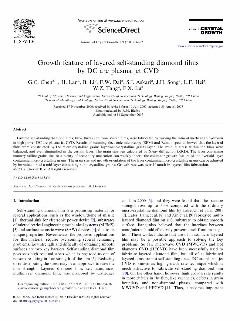
The whole films grown by procedures 1 and 3 possessedupward surface profile. There was no clear curving surfaceprofile in the film obtained by procedure 2. Morphology ofeach film was observed. There was not much differencefrom center to fringe in the films fabricated by procedures 1and 3. Only grain size became larger from center to fringein the film fabricated by procedure 2. Therefore, themorphology of cross section and growth surface of thecenter part of each film is shown in Fig. 2. From Fig. 2a, cand e, the layered structures are clearly distinguished astwo-, three- and four-layered films due to differentdeposition procedure though the boundary between eachlayer is not very straight. The growth surfaces areterminated by cauliflower-like (Fig. 2b and f) or nice-faceted (Fig. 2d) morphology. For two-layered film, thelower layer consists of micrometer-sized columnar crystals,but the upper layer does not. The upper layer weaklyinherits the columnar growth feature of the lower layer.For three-layered film, both the upper layer and the lowerlayer consist of micrometer-sized columnar crystals. How-ever, the grain size in the upper layer is obviously biggerthan that in the lower layer. The mid-layer does not appearto have columnar growth feature. This may be due to shortdeposition time. For four-layered film, the first layer andthe third layer possess micrometer-sized columnar crystals.The grain size in third layer is much smaller than that in the
ARTICLE IN PRESS
Fig. 2. SEM results of as-grown self-standing films: cross section (a) and growth surface (b) of two-layered film; cross section (c) and growth surface (d) of
three-layered film; cross section (e) and growth surface (f) of four-layered film.
G.C. Chen et al. / Journal of Crystal Growth 309 (2007) 86–9288
first layer. This phenomenon is different from thatappearing in the three-layered film. The second layershows weak columnar growth feature that already appearsin two-layered film. In the fourth layer columnar growthfeature does not appear any more. Results in Fig. 2 indicatethat (1) the grain size in the layer with micrometer-sizedcolumnar crystals can be adjusted by introducing adifferent thickness mid-layer; (2) the layer deposited bysecondary nucleation under the condition of high CH4/H2
ratio can inherit the growth feature of the overlaid layer.The inherited growth feature becomes strong or weakdepending on the deposition time. This point can also beseen in other author’s results [9]. Growth rate can becalculated by the thickness divided by deposition time. It isabout 12 mm/h for two-layered film, 10 mm/h for three-layered film and 9 mm/h for four-layered film. That meansthat the growth rate decreases with the increase of the layernumber. It is also found that the deposition rate of layerwith columnar micro-sized crystal is smaller than that ofthe layer deposited under high CH4/H2 ratio condition.This phenomenon has also been mentioned by Sternschulteet al. [14]. The reason is due to more amount of nutritionalradical for diamond growth. Although the growth rates aredifferent, all are about 10 mm/h. This value is much higherthan that in case of fabricating non-self-standing film byHFCVD and MWCVD. This shows the attractive applica-tion of DC arc plasma jet CVD in fabrication of layeredstructure diamond film.
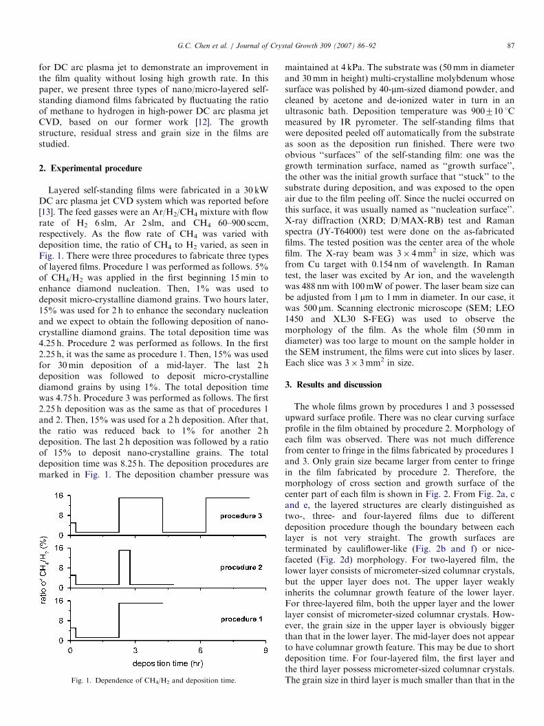
Raman spectra survey was done on the whole films. Thedetected position was in the center of the film which
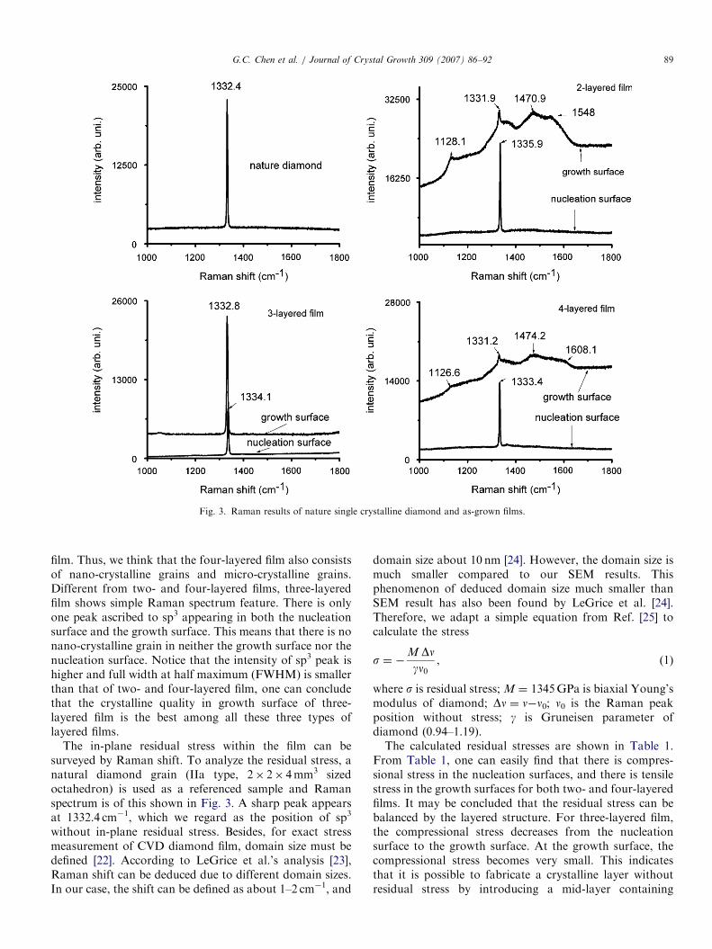
corresponds to SEM result shown in Fig. 2. For eachdetected position, three scans were done to eliminate theerror. Fig. 3 shows the typical results of Raman spectrafrom the nucleation surface and growth surface of thewhole films. For two-layered film, the peak near 1332 cm�1
appears in both the nucleation surface and the growthsurface. It is well known that this peak is ascribed to sp3
band [15]. The intensity of the peak is stronger in thenucleation surface than that in the growth surface. Thisseems to indicate that the concentration of sp3 in thenucleation surface is more than that in the growth surface.There are two other peaks, of these one appears at1128.1 cm�1, and the other one is the broadening peakbetween 1410 and 1620 cm�1, in the growth surface.Nemanich et al. [16] believed that the peak at1128.1 cm�1 was ascribed to nano-sized diamond. How-ever, Ferrari and Robertson regarded it to be due to thescattering of TPA [17]. The broadening peak can bediscomposed to two peaks of which one at 1548 cm�1
ascribed to G-band of sp2 [18], and the other one at1470.9 cm�1 is believed to be relevant with the nanometerdiamond structure [19,20]. This means that the upper layergrown under high ratio of CH4/H2 condition consists ofnano-crystalline diamond. Our former work shows thatthere are nano-sized diamond crystalline grains in the filmwith ‘‘cauliflower’’ morphology [21]. Therefore, we thinkthat the two-layered film consists of the upper layer withnano-crystalline diamond grains and the lower layer is withmicro-crystalline diamond grains. The feature of Ramanspectra in four-layered film is similar to that in two-layered
ARTICLE IN PRESS
Fig. 3. Raman results of nature single crystalline diamond and as-grown films.
G.C. Chen et al. / Journal of Crystal Growth 309 (2007) 86–92 89
film. Thus, we think that the four-layered film also consistsof nano-crystalline grains and micro-crystalline grains.Different from two- and four-layered films, three-layeredfilm shows simple Raman spectrum feature. There is onlyone peak ascribed to sp3 appearing in both the nucleationsurface and the growth surface. This means that there is nonano-crystalline grain in neither the growth surface nor thenucleation surface. Notice that the intensity of sp3 peak ishigher and full width at half maximum (FWHM) is smallerthan that of two- and four-layered film, one can concludethat the crystalline quality in growth surface of three-layered film is the best among all these three types oflayered films.
The in-plane residual stress within the film can besurveyed by Raman shift. To analyze the residual stress, anatural diamond grain (IIa type, 2� 2� 4mm3 sizedoctahedron) is used as a referenced sample and Ramanspectrum is of this shown in Fig. 3. A sharp peak appearsat 1332.4 cm�1, which we regard as the position of sp3
without in-plane residual stress. Besides, for exact stressmeasurement of CVD diamond film, domain size must bedefined [22]. According to LeGrice et al.’s analysis [23],Raman shift can be deduced due to different domain sizes.In our case, the shift can be defined as about 1–2 cm�1, and
domain size about 10 nm [24]. However, the domain size ismuch smaller compared to our SEM results. Thisphenomenon of deduced domain size much smaller thanSEM result has also been found by LeGrice et al. [24].Therefore, we adapt a simple equation from Ref. [25] tocalculate the stress
s ¼ �M Dngn0
, (1)
where s is residual stress; M ¼ 1345GPa is biaxial Young’smodulus of diamond; Dn ¼ n�n0; n0 is the Raman peakposition without stress; g is Gruneisen parameter ofdiamond (0.94–1.19).The calculated residual stresses are shown in Table 1.
From Table 1, one can easily find that there is compres-sional stress in the nucleation surfaces, and there is tensilestress in the growth surfaces for both two- and four-layeredfilms. It may be concluded that the residual stress can bebalanced by the layered structure. For three-layered film,the compressional stress decreases from the nucleationsurface to the growth surface. At the growth surface, thecompressional stress becomes very small. This indicatesthat it is possible to fabricate a crystalline layer withoutresidual stress by introducing a mid-layer containing
ARTICLE IN PRESS
Table 1
Residual stress in as-grown films
Raman
peak
position
(cm�1)
Average
Raman
shift (cm�1)
Average
stress
(g ¼ 1.06)
(GPa)
Nature diamond 1332.4
1332.4 0 –
1332.5
Two-
layered film
Nucleation
surface
1335.9
1335.5 3.367 �3.206
1336.0
Growth
surface
1331.9
1331.7 �0.666 0.6341331.7
Three-
layered film
Nucleation
surface
1334.1
1334.2 1.9 �1.8091334.7
Growth
surface
1332.8
1332.5 0.2 �0.1911332.6
Four-
layered film
Nucleation
surface
1333.4
1333.5 1.0 �0.9521333.4
Growth
surface
1331.2 �1.21331.1 1.1431331.4
G.C. Chen et al. / Journal of Crystal Growth 309 (2007) 86–9290
nano-crystalline grains with proper thickness. Also fromTable 1, one can see that the compressional stress value isdifferent in the nucleation surface from each film, thoughthe deposition parameters are the same. We are inclined tobelieve that the variation of stress value in each film is dueto the overlayer structure. Stress in the film is balanced bythe film body. If the structure or the film body volume isdifferent, the stress distribution will be changed. Thesethree films possess different structures and thickness. Thismay result in the different stress distribution.
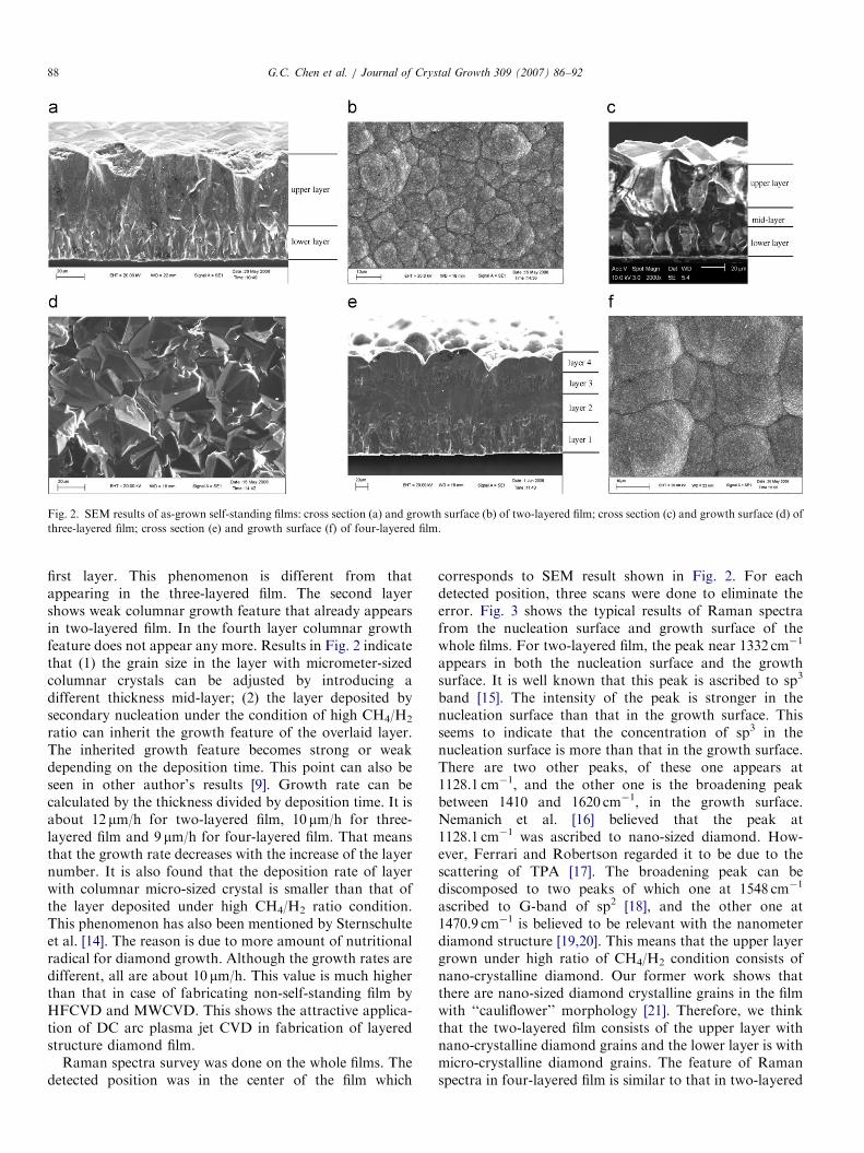
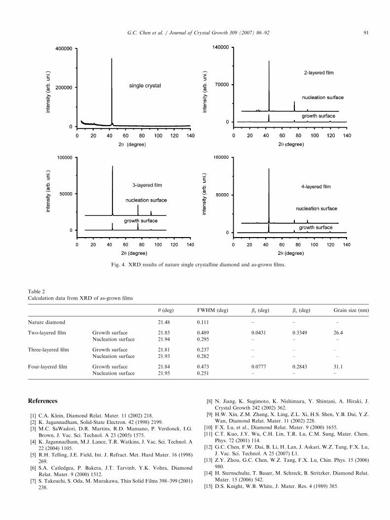
The growth surfaces and the nucleation surfaces of thefilms shown in Fig. 2 were surveyed by XRD. The resultsare shown in Fig. 4. For two- and four-layered film, (1 1 1)-crystalline plane (at 2y ¼ 431) possesses absolutely strongdiffraction intensity while (2 2 0)-crystalline plane (at2y ¼ 741), (3 3 1)-crystalline plane at 2y ¼ 931 and (4 0 0)-crystalline plan at 2y ¼ 1181 possess weak intensity in boththe nucleation surface and the growth surface. Thus, thegrowth orientation is /1 1 1S in both the nucleationsurface and the growth surface. For three-layered film,the feature of XRD spectrum is different from thenucleation surface to the growth surface. It is /1 1 1S-orientation in the nucleation surface, whereas it becomes/1 1 0S-orientation in the growth surface. The transitionof orientation may be due to the mid-layer containingnanometer-sized grain formed by secondary nucleation.This viewpoint has been also mentioned by Zhang andJiang [26].
The FWHM of (1 1 1)-surface diffraction peak fromnatural single-crystal diamond is detected as 0.1111. Forthe as-grown films, the maximum of FWHM, near to 0.51,occurs from growth surfaces of two- and four-layered films.The minimum value, about 0.21, occurs from growthsurface of three-layered film. The FWHM value from allnucleation surfaces is about 0.31. This means that thediffraction peak is broadened. It is known that both thecrystalline grain size and microstrains contribute to the linebroadening in XRD [27,28]. For nano-crystal, the broad-ening due to crystallite size (bc) and lattice strain (be) arerepresented by
bc ¼Kl
D cos y, (2)
be ¼ 4e tan y, (3)
where K is the Scherrer factor, l is the wavelength and y isthe angular position of a certain reflection. D and e,respectively, indicate the grain size and microstrains of thecrystalline phase investigated [29].Based on the results in Table 1, the broadening due to
lattice strain (be) can be deduced from formula (3). Thegrain size (D) can be deduced by Eq. (2) withbc ¼ b�be�b0 (b0 is stress-free FWHM). Therefore, wecan know that the grain sizes of growth surface in two- andfour-layered film are about 26.4 and 31.1 nm, respectively.Formula (3) is suited for nano-crystal, but it cannot bedirectly adopted to calculate micro-crystalline grain size.The FWHM and grain size results are shown in Table 2.
4. Conclusion
Layered diamond films were fabricated by varying theratio of methane to hydrogen in high-power DC arc plasmajet CVD. The film structure consists of the layers contain-ing nano- and micro-crystalline grains. The layer contain-ing nano-crystalline grains due to a plenty of secondarynucleation can weakly inherit the columnar growth featureof the overlaid layer containing micro-crystalline grains.The residual stress in film can be balanced by this layeredstructure, and even can be diminished by a mid-layercontaining nano-crystalline grains with proper thickness.The grain size and growth orientation of the layercontaining micro-crystalline grains can be adjusted byintroduction of a mid-layer containing nano-crystallinegrains. The growth rate was about 10 mm/h in layered filmfabrication.
Acknowledgments
The work is supported by NSFC (No. 50472095), SRFfor ROCS (No. 2003-14), Beijing Novel Project (No.2003A13), and Beijing NSF (No. 2062015).
ARTICLE IN PRESS
Table 2
Calculation data from XRD of as-grown films
y (deg) FWHM (deg) be (deg) bc (deg) Grain size (nm)
Nature diamond 21.48 0.111 – – –
Two-layered film Growth surface 21.85 0.489 0.0431 0.3349 26.4
Nucleation surface 21.94 0.295 – – –
Three-layered film Growth surface 21.81 0.237 – – –
Nucleation surface 21.93 0.282 – – –
Four-layered film Growth surface 21.84 0.473 0.0777 0.2843 31.1
Nucleation surface 21.95 0.251 – – –
Fig. 4. XRD results of nature single crystalline diamond and as-grown films.
G.C. Chen et al. / Journal of Crystal Growth 309 (2007) 86–92 91
References
[1] C.A. Klein, Diamond Relat. Mater. 11 (2002) 218.
[2] K. Jagannadham, Solid-State Electron. 42 (1998) 2199.
[3] M.C. SaWadori, D.R. Martins, R.D. Mansano, P. Verdonck, I.G.
Brown, J. Vac. Sci. Technol. A 23 (2005) 1575.
[4] K. Jagannaclham, M.J. Lance, T.R. Watkins, J. Vac. Sci. Technol. A
22 (2004) 1105.
[5] R.H. Telling, J.E. Field, Int. J. Refract. Met. Hard Mater. 16 (1998)
269.
[6] S.A. Catledgea, P. Bakera, J.T. Tarvinb, Y.K. Vohra, Diamond
Relat. Mater. 9 (2000) 1512.
[7] S. Takeuchi, S. Oda, M. Murakawa, Thin Solid Films 398–399 (2001)
238.
[8] N. Jiang, K. Sugimoto, K. Nishimura, Y. Shintani, A. Hiraki, J.
Crystal Growth 242 (2002) 362.
[9] H.W. Xin, Z.M. Zhang, X. Ling, Z.L. Xi, H.S. Shen, Y.B. Dai, Y.Z.
Wan, Diamond Relat. Mater. 11 (2002) 228.
[10] F.X. Lu, et al., Diamond Relat. Mater. 9 (2000) 1655.
[11] C.T. Kuo, J.Y. Wu, C.H. Lin, T.R. Lu, C.M. Sung, Mater. Chem.
Phys. 72 (2001) 114.
[12] G.C. Chen, F.W. Dai, B. Li, H. Lan, J. Askari, W.Z. Tang, F.X. Lu,
J. Vac. Sci. Technol. A 25 (2007) L1.
[13] Z.Y. Zhou, G.C. Chen, W.Z. Tang, F.X. Lu, Chin. Phys. 15 (2006)
980.
[14] H. Sternschulte, T. Bauer, M. Schreck, B. Stritzker, Diamond Relat.
Mater. 15 (2006) 542.
[15] D.S. Knight, W.B. White, J. Mater. Res. 4 (1989) 385.

ARTICLE IN PRESSG.C. Chen et al. / Journal of Crystal Growth 309 (2007) 86–9292
[16] R.J. Nemanich, J.T. Glass, G. Lucovsky, R.E. Shroder, J. Vac. Sci.
Technol. A 6 (1988) 1783.
[17] A.C. Ferrari, J. Robertson, Phys. Rev. B 63 (2001) 1405.
[18] F. Tuinstra, J.L. Koenig, J. Chem. Phys. 53 (1970) 1126.
[19] H. Yoshikawa, C. Moral, Y. Koga, Diamond Relat. Mater. 10 (2001)
1598.
[20] R. Kapil, B.R. Mehta, V.D. Vankar, C. Roy, A. Pradhan, Thin Solid
Films 322 (1998) 74.
[21] W. Tang, C. Zhu, W. Yao, Q. Wang, C. Li, F. Lu, Thin Solid Films
429 (2003) 63.
[22] H. Windischmann, K.J. Gray, Diamond Relat. Mater. 4 (1995) 837.
[23] Y.M. LeGrice, R.J. Nemanich, J.T. Glass, Y.H. Lee, R.A. Rudder,
R.J. Markunas, Mater. Res. Soc. Sym. Proc. 162 (1990) 219.
[24] R.J. Nemanich, L. Bergman, Y.M. LeGrice, K.F. Turner,
T.P. Humphreys, SPIE—Appl. Spectrosc. Mater. Sci. 1437 (1991) 2.
[25] Z.-Q. Xu, L. Leve, M. Lukitsch, A. Kumar, J. Mater. Res. 22 (2007)
1012.
[26] W.J. Zhang, X. Jiang, Appl. Phys. Lett. 68 (1996) 2195.
[27] Z. Guo, K.G. Keong, W. Sha, J. Alloys Compds. 358 (2003) 112.
[28] K. Santra, P. Chatterjee, S.P. Sen Gupta, Sol. Energy Mater. Sol.
Cells 57 (1999) 345.
[29] L. Zhang, C.Y. Xie, J.S. Wu, J. Alloys Compd. 427 (2007) 238.