Embed Size (px)
Citation preview
Article
Cold Wall CVD (CWCVD) in the Synthesis of Few Layered Graphene on Ni Mohammad Faisal 1,*, Sudipta Bhattacharyya 2, Pika Jha 3, Anil Agarwal 3, P. K. Chaudhury 3, S. S. Islam 4 and M. Husain 5
1 Department of Materials Science and Engineering, Indian Institute of Technology Kanpur, Kanpur 208016, India
2 Research and Innovation Centre, IIT Madras Research Park, Taramani, Chennai 600113, India; [email protected]
3 Solid State Physics Laboratory, Lucknow Road, Timarpur, Delhi 110054, India; [email protected] (P.J.); [email protected] (A.A.); [email protected] (P.K.C.)
4 Department of Applied Science and Humanities, Jamia Millia Islamia, Jamia Nagar, New Delhi 110025, India; [email protected]
5 Department of Physics, Jamia Millia Islamia, New Delhi 110025, India; [email protected] * Corresponding Author: Mohammad Faisal. Ph.: +91-8765696092; Email: [email protected]
Abstract: We report the growth of graphene at a low temperature using the cold wall chemical vapor deposition technique (CWCVD). Few layered (~6-8 layers) graphene were grown on nickel-coated silicon with acetylene as the precursor gas. The advantage of the combination of the acetylene (as a carbon feedstock) and the nickel catalyst was the lowering of the graphene growth temperature. Nickel coated silicon samples were pre-treated (heat treatment in inert atmosphere) before the growth and the effect of the pre-treatment on the catalyst as well as on the grown film was studied. The final samples were characterized with scanning electron microscopy and Raman spectroscopy. In CWCVD route, the heating of only the substrate holder enabled high heating and cooling rates, which, along with the control over partial pressure of the precursor gas had profound effect on the formation of graphene. In the best sample we have achieved almost equal intensity of the G and 2D peaks in Raman spectrum, which implied about ~6-8 layers of Graphene. The defect peak (the D band) was extremely small in the sample and it was attributed to the ripples and the underlying roughness of the nickel film. We analyzed that a proper choice of the thickness of catalyst layer and a higher cooling rate after graphene growth it would be possible to obtain monolayered graphene. Similar samples grown in a normal atmospheric CVD (with some engineered design to promote fast cooling) were also compared with the cold wall CVD grown samples and plasma assisted CWCVD, and cold-wall CVD demonstrated a better control over the quality of graphene film through the fast cooling and a controlled partial pressure of the precursor gas.
Keywords: graphene; chemical vapor deposition; nanomaterials
1. Introduction
After its experimental demonstration with the pioneering work of Noveselov et. al., graphene has triggered a renewed interest both among scientists as well as technologists from different research fields [1]. Graphene is a single layer of carbon atoms arranged in two dimensional lattice in hexagonal manner, the graphene happens to be chemically inactive and posses high strength [2]. The existence of several novel properties like its extremely high electronic mobility [3,4,5,6], ambipolar characteristics [7,8], high optical transparency [9,10,11,12], high surface to volume ratio [13,14], mechanical strength [15,16], make graphene an exotic material for a wide range of applications.
From the application point of view in electronic industry [3,4,5,6] and in many other structural applications which require composite materials, graphene can be seen as a vital reinforcing component [13]. Tremendous amount of research has been concentrated towards the development of
Preprints (www.preprints.org) | NOT PEER-REVIEWED | Posted: 30 May 2017 doi:10.20944/preprints201705.0217.v1
© 2017 by the author(s). Distributed under a Creative Commons CC BY license.
2 of 9
the low cost and feasible synthesis routes for better quality and uniform graphene sheet with monolayer structure.
Monolayered graphene can be synthesized in many ways and the most common routes is are CVD, mechanical exfoliation of highly oriented pyrolytic graphite (HOPG) [1,17], graphite oxide reduction [18], SiC wafers graphitization under ultra-high vacuum [19]. Since the size of the graphene samples obtained from techniques like mechanical exfoliation were are usually very small (tens of microns) for most of the applications or are expensive to grow on large area samples, chemical vapor deposition technique on transition metal catalyst supported on inert silicon substrate gained more attention because of its large area coverage and relatively cheaper cost. [2,20–27], many others like.
Here we report the successful growth of graphene on nickel substrates using cold wall chemical vapor deposition technique under different conditions like temperature, total pressure and varying partial pressure of acetylene, the precursor gas. The use of CWCVD enabled a fast cooling in a simple processing set-up, and hence helped in obtaining the right amount of carbon precipitation necessary for graphene formation. The quality of films was assessed by Raman spectroscopy and the defects were related to the pre-treatment as well as the deposition mechanism.
2. Experimental details
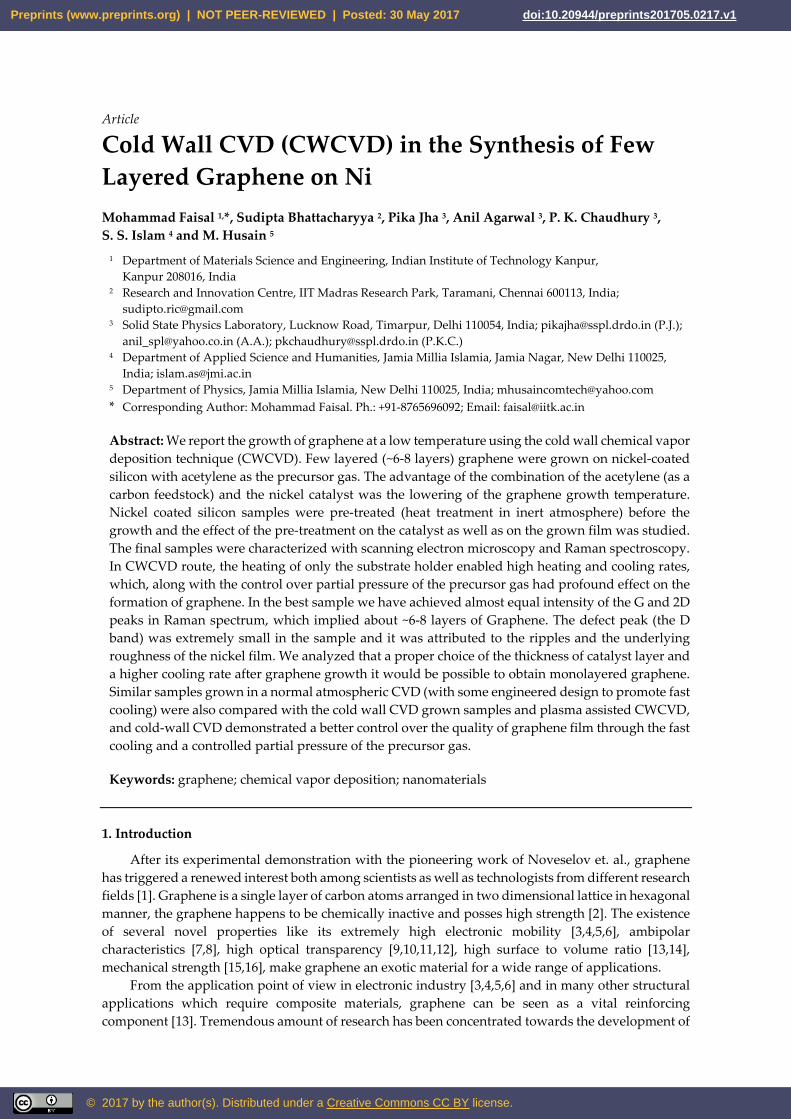
The growth was carried out in an existing PECVD chamber [without using the plasma source] with its walls cooled by water and fitted with gas lines to introduce the precursor like acetylene and the carrier gas like hydrogen. The tube diameter of 2.5 cm and the length of the tube is 25 cm. The schematic of the gas connections along with the growth chamber is depicted in Figure 1.
Figure 1. Schematic representation of Cold Walled Chemical Vapor Deposition (CWCVD) apparatus along with the various gases used as precursor (H2, C2H2, Ar). The gas flow is controlled with mass flow controllers. The two or more gases were mixed together using gas mixture. The sample holder rests on PBN heater, controlled by external power source. The temperature is measured using K-type thermocouple. Very fast cooling rates were achieved using chiller at 15°C and water circulating copper tubes.
MFC 1
MFC 2
MFC 3 MFC4
FURNACE
QUARTZ TUBE
EXHAUST
SUBSTRATE- HOLDER
SUBSTRATE
GAS MIXTURE
INLET
ROTARY PUMP
THERMOCOUPLE
GAS HEADER
SHUT- OFF VALVE
ROTAMETER
O2
N2
C2H2
H2
NH3
H2 PURIFIER
COMPOUND GAUGE
PBN Heater
Water cooled copper tubes
Preprints (www.preprints.org) | NOT PEER-REVIEWED | Posted: 30 May 2017 doi:10.20944/preprints201705.0217.v1
3 of 9
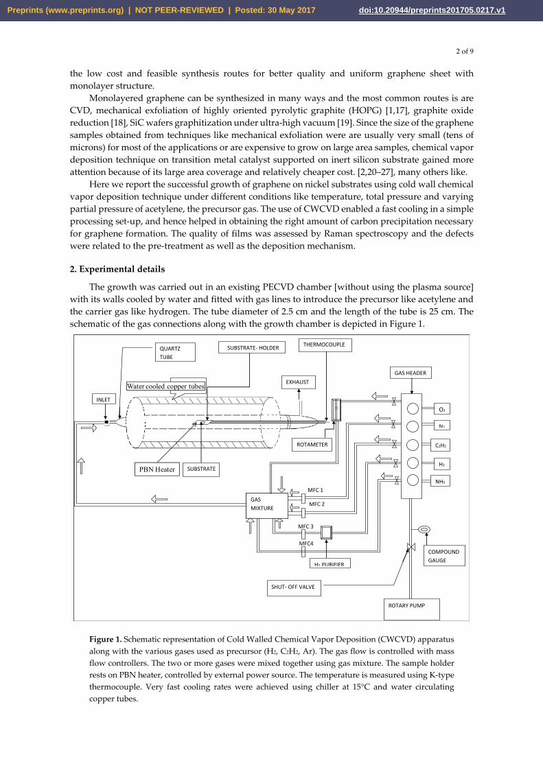
The substrate was Si/SiO2 wafers (n-type (100)) 10Χ10 mm rectangular piece with a catalyst layer (Ni) deposited by RF sputtering (operating at 200 watt and the deposition time was 13 min.). The thickness of the nickel film on substrate was from ~100-300 nm as measured from optical profilometer. The substrate coated with nickel film is then treated with continuous flow of argon ~100 sccm for 15 min. followed by H2 gas purging at room temperature for 15 min. after this H2 gas is stopped. In the presence of argon gas alone before growth the catalyst layers were annealed from room temperature to ~1000 °C to improve the crystallinity in the nickel film and also to expose fresh Ni surface by reducing any possible nickel oxide. The pre treated samples were used for growth at temperature ranging from 550-750 °C (700 °C, 650 °C, 600 °C), the range of temperatures were used to find out the optimum growth temperature. The substrate heater was a suspended boron nitride heater capable of heating/cooling at a rate more than 100 °C/min. Tip of thermocouple (K-type) is placed on top face of the nickel film. The walls of the reactor chamber were water cooled with DI water circulating through chilling unit maintained at 15 °C and flowing through copper tubes (copper tubes are in close contact to the body of the reactor chamber). The reactor chamber is evacuated down to rough vacuum (10−3 Torr). H2 gas is flushed under cold conditions for 15 more minutes. At the growth temperature (700 °C, 650 °C and 600 °C) combination of H2 and C2H2 (as a carbon precursor) gases at a total gas pressure of ~0.8 Torr in the flow ratio of 2:1is used. The growth was carried out for different times, two and five min. to study the effect of growth time. After the completion of growth; power source was switched off and simultaneously carbon source was also switched off, drastic quenching with cooling rates above 300 °C /min. were achieved (combined effect of cooling from boron nitride heater and chilling copper coils). Similar experiments were carried out by varying growth parameters (gas flow rates, growth time, cooling rates, Ni catalyst film thickness, etc.) for optimizing the growth parameters. In total we studied six samples (S1, S2, S3, S4, S5 and S6) with different combination of growth parameters (temperature, partial pressure of precursor gases, growth time and cooling rates). Schematic representation of the entire growth process for graphene growth is presented inFigure 2.
Figure 2. Schematic representation of the growth mechanism of the graphene growth on Ni catalyst supported on silicon substrate via cold walled chemical vapor deposition technique. Ni catalyst is sputter deposited on silicon substrate up to a thickness ~100-300 nm. Ni catalyst layer is heat treated under argon atmosphere for the recrystallization of Ni film at ~1000 °C. Precursor gases (H2 & C2H2) is used in the ratio of 2:1 for the growth time of 2 to 5 min at growth temperatures (700 °C, 650 °C and 650 °C). Few layered (~6-8 layers) graphene is obtained.
Preprints (www.preprints.org) | NOT PEER-REVIEWED | Posted: 30 May 2017 doi:10.20944/preprints201705.0217.v1
4 of 9
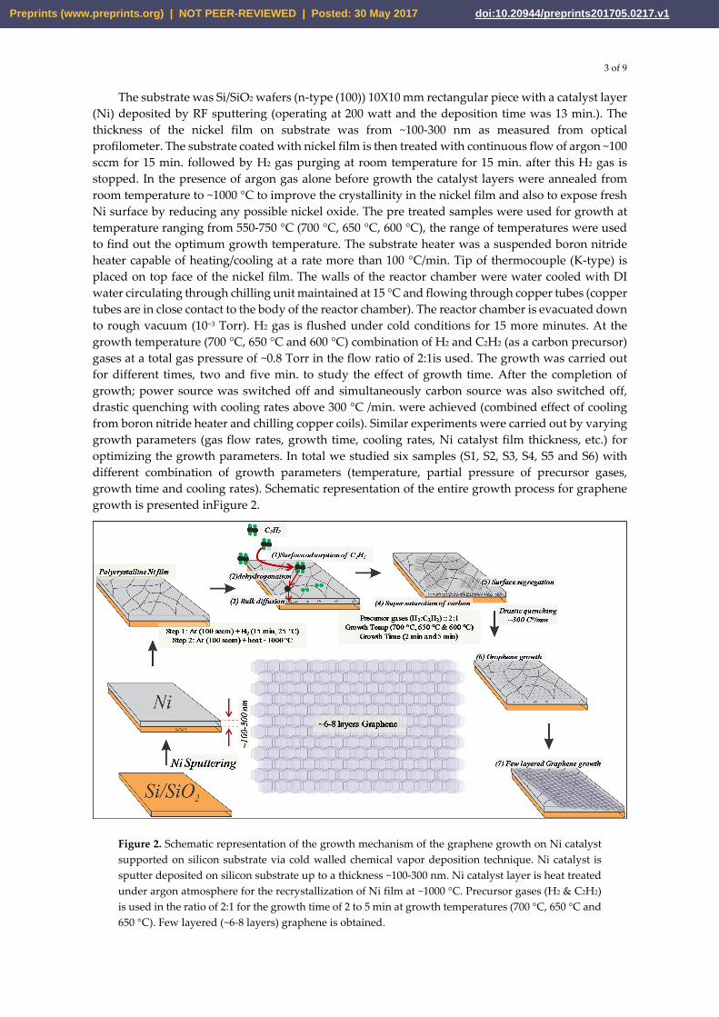
Table 1 provides the detail of the parameters used during the graphene growth. SEM in secondary electron mode for topographical evidences and Raman characterization for different molecular forms of carbon signatures were carried out with Raman excitation wavelength of 488 nm. An experiment is also performed to see the presence of graphene under scanning electron microscopy using a graphite pencil. Starting material was a graphite pencil, a scotch tape and a Si wafer. Pencil graphite was rubbed against Si wafer and a small piece of scotch tape is then placed over the rubbed area with glue face facing towards the rubbed area, then the scotch tape piece was peeled from the wafer and a new piece (second piece) of scotch tape is now stick to the old piece (with the glue face facing towards each other), these two pieces are again peeled away from each other and again a new piece (third piece) of scotch tape is now pasted with the second piece and again peeled away, this was repeated for 100 times and then the last piece of scotch tape is pasted to the new piece of Si wafer. The Si wafer is then taken to SEM characterization.
Table 1. Details the various growth parameters like growth temperature in degree celcius for graphene, precursor gas flow rate in sccm and growth time in min.
3. Results and discussions
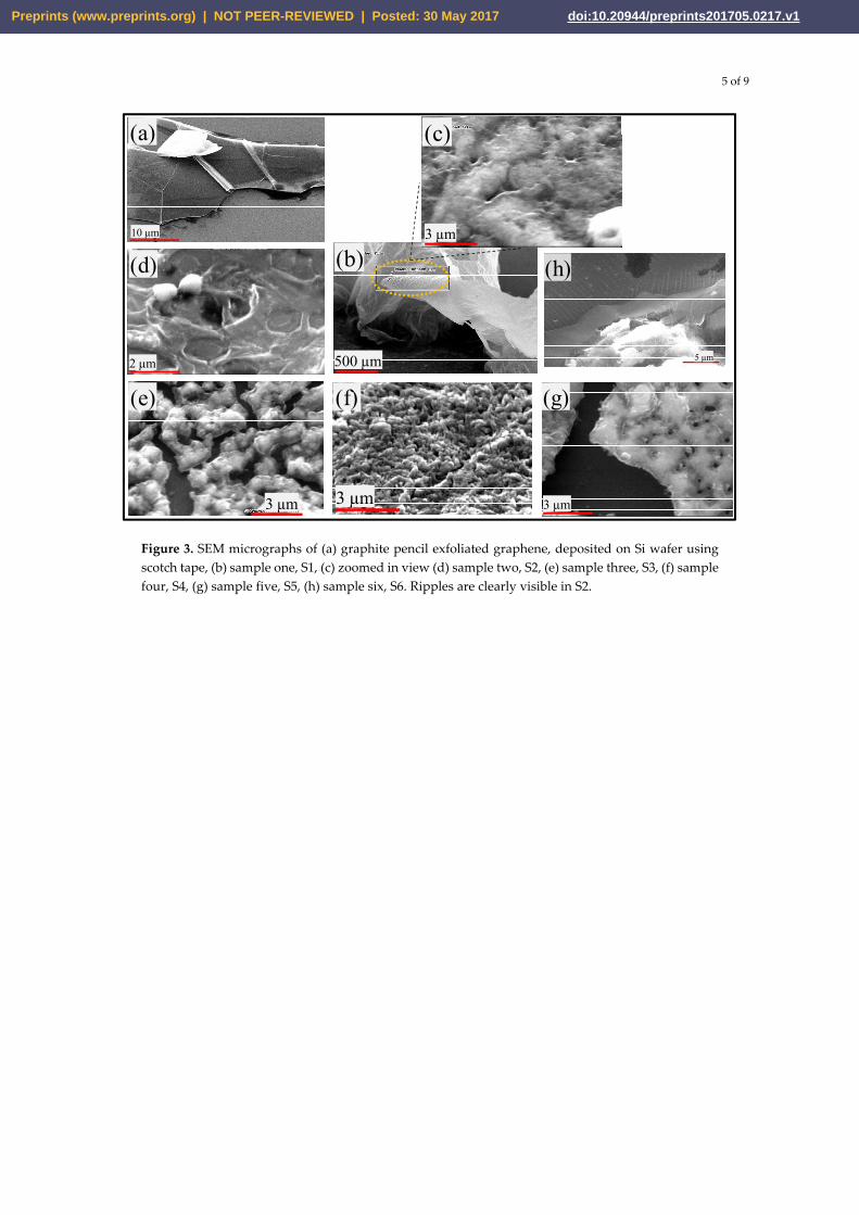
The scanning electron micrograph of a typical graphene film is shown in Figure 3 for all the samples ranging from S1 to S6 with different growth parameters as described in Table 1. It might be noted that sample 1 and 2 are parts of the same sample, where, some parts flaked of from the same (sample 1) and it was interesting to see if these parts had the same characteristics. These flakes had most likely formed due to thermal stress developed in the nickel catalyst at certain regions and hence a localized dewetting of the catalyst layer, which was noticed before.
Figure 3 (a) shows SEM micrograph of graphite pencil exfoliated graphene film on Si wafer, this gave us a better insight of the visual observation of graphene layer under SEM. Sample S1 shows a free standing graphite flake as can be seen in the Figure 3 (b), the morphology was closely examined as can be seen in the Figure 3 (c). We can see that the surface of the flake has prominent ripples or wavy character. This waviness in the film could result in D band in Raman which could be the due to sp3 character as a result of curvature in graphene film. The next sample in the series, S2, as well shows the ripples in the SEM micrograph as is evident in Figure 3 (d) and also shows D band signal in Raman spectrum in Figure 5. SEM micrographs of samples S3 (Figure 3 (e)), S4 (Figure 3 (f)), S5 (Figure 3 (g)) S6 (Figure 3 (h)) also show waviness in the graphene films deposited under different growth parameters, these samples also show a small D band as is seen in Raman spectrum of the corresponding samples in Figure 5. The very reason for the presence of waviness in the graphene films deposited can arise due to either the relatively small domains (large number of domain boundaries) or the underlying nickel catalyst which was roughened during the pre-treatment and one can also observe the existence of a thin layer above the catalyst.
S 1 S 2 S 3 S 4 S 5 S 6Annealing Temperature (°C) 970 970 970 970 970 970
Ar flow (sccm) (annealing) 100 100 100 100 100 100
Growth Temperature (°C) 700 700 700 650 600 650
Growth Time (min) 5 5 2 2 2 2
H2 flow rate (sccm) (growth) 24 24 24 24 24 24
C2H2 flow rate (sccm) (growth) 12 12 12 12 12 24
Cooling rate (°C/min) 300 300 300 300 300 300
I2D/IG0.7 0.83 0.96 0.92 0.92 1.07
ID/IG0.33 0.45 0.72 0.51 0.41 0.38
Preprints (www.preprints.org) | NOT PEER-REVIEWED | Posted: 30 May 2017 doi:10.20944/preprints201705.0217.v1
5 of 9
Figure 3. SEM micrographs of (a) graphite pencil exfoliated graphene, deposited on Si wafer using scotch tape, (b) sample one, S1, (c) zoomed in view (d) sample two, S2, (e) sample three, S3, (f) sample four, S4, (g) sample five, S5, (h) sample six, S6. Ripples are clearly visible in S2.
10 µm
(a)
2 µm
(d)
3 µm
(e)
3 µm
(f)
3 µm
(g)
500 µm
3 µm
(c)
(b)
5 µm
(h)
Preprints (www.preprints.org) | NOT PEER-REVIEWED | Posted: 30 May 2017 doi:10.20944/preprints201705.0217.v1
6 of 9
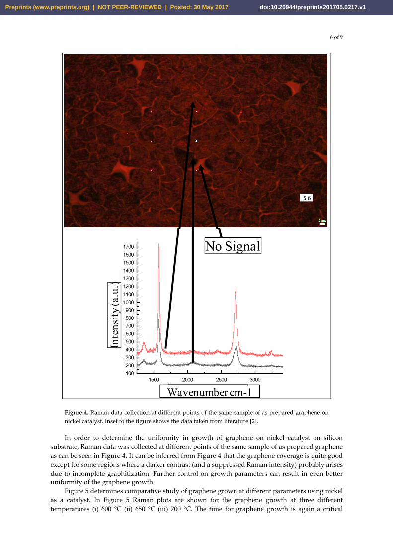
Figure 4. Raman data collection at different points of the same sample of as prepared graphene on nickel catalyst. Inset to the figure shows the data taken from literature [2].
In order to determine the uniformity in growth of graphene on nickel catalyst on silicon substrate, Raman data was collected at different points of the same sample of as prepared graphene as can be seen in Figure 4. It can be inferred from Figure 4 that the graphene coverage is quite good except for some regions where a darker contrast (and a suppressed Raman intensity) probably arises due to incomplete graphitization. Further control on growth parameters can result in even better uniformity of the graphene growth.
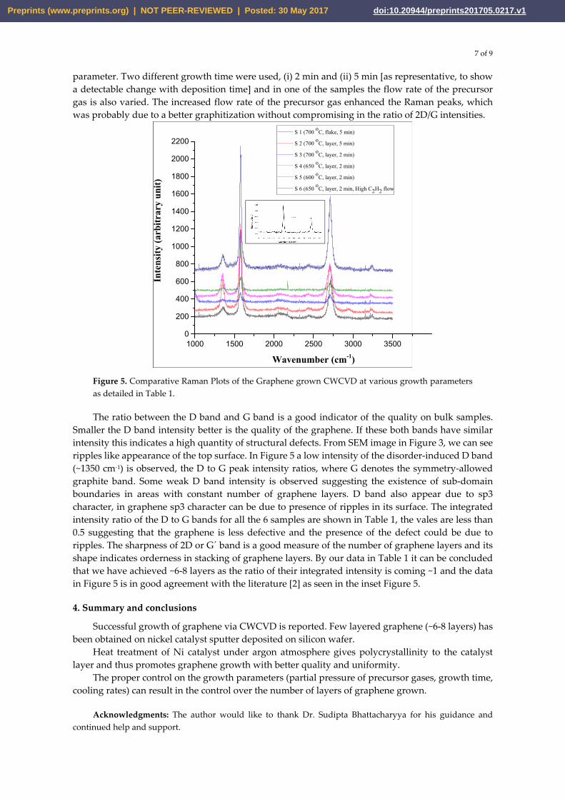
Figure 5 determines comparative study of graphene grown at different parameters using nickel as a catalyst. In Figure 5 Raman plots are shown for the graphene growth at three different temperatures (i) 600 °C (ii) 650 °C (iii) 700 °C. The time for graphene growth is again a critical
S 6
1500 2000 2500 3000100200300400500600700800900
10001100120013001400150016001700 No Signal
Inte
nsity
(a.u
.)
Wavenumber cm-1
Preprints (www.preprints.org) | NOT PEER-REVIEWED | Posted: 30 May 2017 doi:10.20944/preprints201705.0217.v1
7 of 9
parameter. Two different growth time were used, (i) 2 min and (ii) 5 min [as representative, to show a detectable change with deposition time] and in one of the samples the flow rate of the precursor gas is also varied. The increased flow rate of the precursor gas enhanced the Raman peaks, which was probably due to a better graphitization without compromising in the ratio of 2D/G intensities.
Figure 5. Comparative Raman Plots of the Graphene grown CWCVD at various growth parameters as detailed in Table 1.
The ratio between the D band and G band is a good indicator of the quality on bulk samples. Smaller the D band intensity better is the quality of the graphene. If these both bands have similar intensity this indicates a high quantity of structural defects. From SEM image in Figure 3, we can see ripples like appearance of the top surface. In Figure 5 a low intensity of the disorder-induced D band (~1350 cm-1) is observed, the D to G peak intensity ratios, where G denotes the symmetry-allowed graphite band. Some weak D band intensity is observed suggesting the existence of sub-domain boundaries in areas with constant number of graphene layers. D band also appear due to sp3 character, in graphene sp3 character can be due to presence of ripples in its surface. The integrated intensity ratio of the D to G bands for all the 6 samples are shown in Table 1, the vales are less than 0.5 suggesting that the graphene is less defective and the presence of the defect could be due to ripples. The sharpness of 2D or G´ band is a good measure of the number of graphene layers and its shape indicates orderness in stacking of graphene layers. By our data in Table 1 it can be concluded that we have achieved ~6-8 layers as the ratio of their integrated intensity is coming ~1 and the data in Figure 5 is in good agreement with the literature [2] as seen in the inset Figure 5.
4. Summary and conclusions
Successful growth of graphene via CWCVD is reported. Few layered graphene (~6-8 layers) has been obtained on nickel catalyst sputter deposited on silicon wafer.
Heat treatment of Ni catalyst under argon atmosphere gives polycrystallinity to the catalyst layer and thus promotes graphene growth with better quality and uniformity.
The proper control on the growth parameters (partial pressure of precursor gases, growth time, cooling rates) can result in the control over the number of layers of graphene grown.
Acknowledgments: The author would like to thank Dr. Sudipta Bhattacharyya for his guidance and continued help and support.
1000 1500 2000 2500 3000 35000
200
400
600
800
1000
1200
1400
1600
1800
2000
2200 S 1 (700 oC, flake, 5 min)
S 2 (700 oC, layer, 5 min)
S 3 (700 oC, layer, 2 min)
S 4 (650 oC, layer, 2 min)
S 5 (600 oC, layer, 2 min)
S 6 (650 oC, layer, 2 min, High C2H2 flow
Inte
nsity
(arb
itrar
y un
it)
Wavenumber (cm-1)
Preprints (www.preprints.org) | NOT PEER-REVIEWED | Posted: 30 May 2017 doi:10.20944/preprints201705.0217.v1
8 of 9
References
1. K. S. Novoselov, A. K. Geim, S. V. Morozov, D. Jiang, Y. Zhang, S. V. Dubonos, I. V. Grigorieva, and A. A. Firsov,Electric field effect in atomically thin carbon films, Science, 306, 666 (2004).
2. G. Nandamuri, S. Roumimov and R. Solanki, Chemical vapor deposition of graphene films, Nanotechnology, 21, 145604, (2010).
3. S. Wang, P.K. Ang, Z. Wang, A. L. L. TangJ.T.L Thong, K.P. Loh, High mobility, printable, and solution processed graphene electronics, Nano Lett., 10, 92-98, (2010)
4. K.I. Bolotin, K.J. Sikes, Z. Jiang, M. Klima, G. Fudenberg, J. Hone, P. Kim and H.L. Stormer, Ultrahigh electron mobility in suspended graphene, Solid State Communications, 146, 351-355, (2008).
5. M. C. Lemme, T.J. Echtermeyer, M. Baus, B.N Szafranek, J. Bolten, M. Schmidt, T. Wahlbrink and H. Kurz, Mobility in graphene double gate field effect transistors, Solid State Electronics, 52, 514-518, (2008).
6. L. A. Ponomarenko, R. Yang, T. M. Mohiuddin, M. I. Katsnelson, K. S. Novoselov, S. V. Morozov, A. A. Zhukov, F. Schedin, E. W. Hill and A. K. Geim, Effect of high-K environment on charge carrier mobility in graphene, PRL, 102, 206603, (2009).
7. Wang, Han; Hsu, Allen; Wu, Justin; Kong, Jing; Palacios, Tomas, Graphene based ambipolar RF mixers, IEEE Electron Device Letter, 31, 9, (2010).
8. E. Sano1 and T. Otsuji, Source and drain structures for suppressing ambipolar characteristics of graphene field-effect transistors, Applied Physics Express 2, 061601, (2009).
9. G. Eda, G. Fanchini & M. Chhowalla, Large-area ultrathin films of reduced graphene oxide as a transparent and flexible electronic material, Nature Nanotechnology, 3, 270-274, (2008).
10. R. R. Nair, P. Blake, A. N. Grigorenko, K. S. Novoselov, T. J. Booth, T. Stauber, N. M. R. Peres, A. K. Geim, Fine Structure Constant Defines Visual Transparency of Graphene, Science, 320, 1308, (2008).
11. X. Wang , L. Zhi and K. Müllen, Transparent, Conductive Graphene Electrodes for Dye-Sensitized Solar Cells, Nano Lett. 8(1), 323-327, (2008).
12. D. E. Sheehy and J. Schmalian, Optical transparency of graphene as determined by the fine-structure constant, Physical Review B, 80, 193411, (2009).
13. S. Stankovich, D. A. Dikin, G. H. B. Dommett , K. M. Kohlhaas, E. J. Zimney , E. A. Stach, R. D. Piner , S. T. Nguyen & R. S. Ruoff, Graphene based composite materials, nature, 442, 282-286, (2006).
14. S. M Paek, E. J. Yoo and I. Honma, Enhanced cyclic performance and lithium storage capacity of SnO2/graphene nanoporous electrodes with three-dimentionally delaminated flexible structure, Nano Lett, 9, 72-75, (2009).
15. C. Lee, X. Wei, J. W. Kysar, J. Hone, Measurement of elastic properties and intrinsic strength of monolayer graphene, Science, 321, 385-388, (2008).
16. H. Chen, M. B. Müller, K. J. Gilmore, G. G. Wallace, D. Li, Mechanically Strong, Electrically Conductive, and Biocompatible Graphene Paper, Advanced, Materials, 20, 3557-3561, (2008).
17. X. Liang, Z. Fu and S.Y. Chou, Graphene segregated on Ni surfaces and transferred to insulators, Nano let., 7, 3840, (2007).
18. S. Stankovich, D. A. Dikin, R. D. Piner, K. A. Kohlhaas, A. Kleinhammes, Y. Jia, Y.Wu, S. T. Nguyen, R. S. Ruoff, Synthesis of graphene-based nanosheets via chemical reduction of exfoliated graphite oxide, Carbon, 45, 1558-1565, (2007).
19. K. V. Emtsev, A. Bostwick, K. Horn, J. Jobst, G. L. Kellogg, L. Ley, J. L. McChesney, T. Ohta, S. A. Reshanov, J. Röhrl, E. Rotenberg, A. K. Schmid, D. Waldmann, H. B. Weber and T. Seyller ,Towards wafer-size graphene layers by atmospheric pressure graphitization of silicon carbide, Nature Materials, 8, 203-207, (2009).
20. M. Losurdo, M. M. Giangregorio, P. Capezzuto and G. Bruno, Graphene CVD growth on copper and nickel: role of hydrogen in kinetics and structure, Phys. Chem. Chem. Phys, 13, 20836-20843, (2011).
21. X. Wang, H. You, F. Liu, M. Li, L. Wan, S. Li, Q. Li, Y. Xu, R. Tian, Z. Yu, D. Xiang and J. Cheng, Large-scale synthesis of few-layered graphene using CVD, Chem. Vap. Deposition, 15, 53-56, (2009).
22. H. J. Park, J. Meyer, S. Roth, V. S. kalova´, Growth and properties of few-layer graphene prepared by chemical vapor deposition, Carbon, 48, 1088-1094, (2010).
23. J. D. Wood, S. W. Schmucker, A. S. Lyons, E. Pop, J. W. Lyding, Effect of polycrystalline Cu substrate on graphene growth by chemical vapor deposition, Nano Lett, 11, 4547-4554, (2011).
Preprints (www.preprints.org) | NOT PEER-REVIEWED | Posted: 30 May 2017 doi:10.20944/preprints201705.0217.v1

9 of 9
24. B. Hu, H. Ago, Y. Ito, K. Kawahara, M. Tsuji, E. Magome, K. Sumitani, N. Mizuta, K. Ikeda and S. Mizuno, Epitaxial growth of large-area single-layer graphene over Cu(111)/sapphire by atmospheric pressure CVD, Carbon, 50, 57-65, (2012).
25. Alfonso Reina, Xiaoting Jia, John Ho, Daniel Nezich, Hyungbin Son, Vladimir Bulovic, Mildred S. Dresselhaus and Jing Kong, Large Area, Few-Layer Graphene Films on Arbitrary Substrates by Chemical Vapor Deposition, Nano Letters, 9, 30-35, (2009).
26. Robert S. Weatherup, Bruno Dlubak, and Stephan Hofmann, Kinetic Control of Catalytic CVD for High-Quality Graphene at Low Temperatures, ACS Nano, 6, 9996-10003, (2012).
27. Daniel Q. McNerny1, B. Viswanath2, Davor Copic1, Fabrice R. Laye, Christophor Prohoda, Anna C. Brieland-Shoultz, Erik S. Polsen, Nicholas T. Dee, Vijayen S. Veerasamy & A. John Hart, Kinetic Control of Catalytic CVD for High-Quality Graphene at Low Temperatures, Scientific Reports, 4, 2329-2339, (2014).
Preprints (www.preprints.org) | NOT PEER-REVIEWED | Posted: 30 May 2017 doi:10.20944/preprints201705.0217.v1
![Research Article Structural and Morphological Properties ...downloads.hindawi.com/journals/amse/2014/780206.pdf · synthesis method [ ], chemical vapor deposition (CVD) [ ], precipitation](https://img.pdfslide.us/doc/110x75/60625d6e71df443a0601ac47/research-article-structural-and-morphological-properties-synthesis-method-.jpg)