Embed Size (px)
Citation preview
Growth and oxidization stability of cubic Zr1-
xGdxN solid solution thin films
Carina Höglund, Björn Alling, Jens Jensen, Lars Hultman, Jens Birch and R. Hall-Wilton
Linköping University Post Print
N.B.: When citing this work, cite the original article.
Original Publication:
Carina Höglund, Björn Alling, Jens Jensen, Lars Hultman, Jens Birch and R. Hall-Wilton,
Growth and oxidization stability of cubic Zr1-xGdxN solid solution thin films, 2015, Journal
of Applied Physics, (117), 19, 195301.
http://dx.doi.org/10.1063/1.4921167
Copyright: American Institute of Physics (AIP)
http://www.aip.org/
Postprint available at: Linköping University Electronic Press
http://urn.kb.se/resolve?urn=urn:nbn:se:liu:diva-119249
Growth and oxidization stability of cubic Zr1−xGdxN solid solution thin filmsC. Höglund, B. Alling, J. Jensen, L. Hultman, J. Birch, and R. Hall-Wilton Citation: Journal of Applied Physics 117, 195301 (2015); doi: 10.1063/1.4921167 View online: http://dx.doi.org/10.1063/1.4921167 View Table of Contents: http://scitation.aip.org/content/aip/journal/jap/117/19?ver=pdfcov Published by the AIP Publishing Articles you may be interested in Phase stability of ScN-based solid solutions for thermoelectric applications from first-principles calculations J. Appl. Phys. 114, 073512 (2013); 10.1063/1.4818415 Strong electron correlations stabilize paramagnetic cubic Cr1−xAlxN solid solutions Appl. Phys. Lett. 102, 031910 (2013); 10.1063/1.4788747 Mixing thermodynamics of TM 1 − x Gd x N ( TM = Ti , Zr , Hf ) from first principles Appl. Phys. Lett. 98, 241911 (2011); 10.1063/1.3600059 Wurtzite structure Sc 1 − x Al x N solid solution films grown by reactive magnetron sputter epitaxy: Structuralcharacterization and first-principles calculations J. Appl. Phys. 107, 123515 (2010); 10.1063/1.3448235 Degradation of ZrN films at high temperature under controlled atmosphere J. Vac. Sci. Technol. A 22, 2071 (2004); 10.1116/1.1786308
[This article is copyrighted as indicated in the article. Reuse of AIP content is subject to the terms at: http://scitation.aip.org/termsconditions. Downloaded to ] IP:
130.236.83.172 On: Thu, 18 Jun 2015 08:45:00
Growth and oxidization stability of cubic Zr12xGdxN solid solution thin films
C. H€oglund,1,2,a) B. Alling,2,3 J. Jensen,2 L. Hultman,2 J. Birch,2 and R. Hall-Wilton1,4
1European Spallation Source ESS AB, P.O. Box 176, SE-221 00 Lund, Sweden2Department of Physics, Chemistry and Biology (IFM), Thin Film Physics Division, Link€oping University,SE-581 83 Link€oping, Sweden3Max-Planck-Institut f€ur Eisenforschung GmbH, D-402 37 D€usseldorf, Germany4Mid-Sweden University, SE-851 70 Sundsvall, Sweden
(Received 27 March 2015; accepted 28 April 2015; published online 15 May 2015)
We report Zr1�xGdxN thin films deposited by magnetron sputter deposition. We show a solid
solubility of the highly neutron absorbing GdN into ZrN along the whole compositional range,
which is in excellent agreement with our recent predictions by first-principles calculations. An oxi-
dization study in air shows that Zr1�xGdxN with x reaching from 1 to close to 0 fully oxidizes, but
that the oxidization is slowed down by an increased amount of ZrN or stopped by applying a cap-
ping layer of ZrN. The crystalline quality of Zr0.5Gd0.5N films increases with substrate tempera-
tures increasing from 100 �C to 900 �C. VC 2015 Author(s). All article content, except whereotherwise noted, is licensed under a Creative Commons Attribution 3.0 Unported License.
[http://dx.doi.org/10.1063/1.4921167]
INTRODUCTION
Gadolinium compounds and their alloys are of interest
due to the high thermal neutron absorption cross-section of
Gd and due to its magnetic properties. Among all naturally
occurring elements, Gd has the highest thermal neutron
absorption cross-section of 49 700 b. One of its stable iso-
topes, 157Gd, with a natural abundance of 15.65% has an
absorption cross-section as high as 259 000 b and is commer-
cially available. Gd is ferromagnetic at temperatures below
289 K, which makes it a common element in ferromagnetic
superconductors. At higher temperature it is strongly para-
magnetic, resulting in Gd(III) chelates being the leading con-
trast agents in magnetic resonance imaging.1
The high probability of Gd to absorb thermal neutrons
enables new types of neutron detectors that could raise detec-
tor resolution and detection efficiency to a completely new
level. A second application is found within thermal neutron
shielding, where the nowadays very large and heavy materi-
als could be replaced by micro-engineered and miniaturized
solutions.2 New large-scale neutron scattering facilities like
the European Spallation Source (ESS)3 and target station 2
at the Spallation Neutron Source (SNS)4 are striving to push
the limits within these fields with requirements that are not
yet fulfilled by state of the art technologies. In addition to
the enhanced requirements there is a severe shortage in the
supply of 3He gas,5,6 the nowadays primarily used neutron
absorbing and converting material in neutron detectors. This
has forced the community to search for alternative solu-
tions7,8 and the boron isotope 10B is seen as one of the most
promising replacements.9–15 The main options are technolo-
gies based on 10B4C thin films and this is a field in which the
authors’16–18 and Nowak and co-workers’19 research and de-
velopment work have enabled rapid progress. These types of
detectors are mainly intended for use in large area gaseous
neutron detectors and a significant fraction of the detectors at
the ESS will be based on this technology.20,21 A limitation of
the 10B4C technology is the relatively low efficiency of a
few percent for one layer of 10B4C to absorb and convert a
neutron into the two reaction particles 7Li and 4He (10Bþ n
! 7Liþ 4Heþ c) and to detect those.22,23 The solution has
been to collect the neutrons over several layers,9,24–27 result-
ing in the detector mechanics being the limiting factor for
the spatial resolution. Instead, a detector containing only
one, several micrometer thick, layer of Gd could provide an
efficiency of approximately 20%, or around 50% if the iso-
tope 155Gd or 157Gd is used.28,29 Such a detector would fulfill
the efficiency and resolution requirements of 20% and
<0.2 mm, respectively, and allow for parallax corrections in
the varying sample-detector distance setup in the Neutron
Macromolecular Crystallography (NMX) instrument that
will be built at the ESS.3 Initial studies on the potential of
solid neutron converters in combination with micro pattern
gaseous detectors have been reported.30 Schulz and
co-workers developed micro-strip gas chambers (MSGC)31
that contain neutron converting layers of Gd29,32 and in par-
allel Sauli developed gas electron multiplication (GEM) neu-
tron detectors, which can be an alternative to MSGCs.33
Both technologies have the potential to be used in an instru-
ment like NMX, but require long-term stable thin films con-
taining high amounts of Gd. GdN, which has a higher Gd
content per unit volume than Gd2O334 or even pure Gd could
be a suitable solution.
The reduction of experimental backgrounds for neutron
spallation sources is a very topical issue35 and instrument
performance is typically defined by signal-to-background
ratios. While the signal is defined by the intensity of the
source, the background can be improved with more advanced
instrument designs, resulting in improved performances.
Additionally, large volumes of radiation shielding are
required and, therefore, significant cost savings are expected
for advances in the search for new effective materials.2,36a)Email: [email protected]. Tel.: þ46 72 179 2023.
0021-8979/2015/117(19)/195301/6 VC Author(s) 2015117, 195301-1
JOURNAL OF APPLIED PHYSICS 117, 195301 (2015)
[This article is copyrighted as indicated in the article. Reuse of AIP content is subject to the terms at: http://scitation.aip.org/termsconditions. Downloaded to ] IP:
130.236.83.172 On: Thu, 18 Jun 2015 08:45:00
Whilst the work this far has concentrated on reducing fast
neutron and gamma ray background, there is also an effort
needed in reducing the background from thermal neutrons
preventing “cross-talk” between local neutron detector ele-
ments. Using Gd compounds, neutron shielding can be engi-
neered to be both compact and very efficient. At the
moment, this is typically solved by using Gd in the form of
Gd2O3 that is mixed with an epoxy and painted onto surfaces
to be shielded, but epoxy is not ideal due to outgassing and
does not allow for something mechanically precise.
Therefore, stable Gd-rich compounds that are precisely de-
posited as thin films present a potential application niche.
During the past ten years, it has been shown that
rocksalt-structured GdN thin films can be grown both with
physical vapor deposition techniques like reactive sputter-
ing,37–40 reactive thermal evaporation,41–43 and molecular
beam epitaxy,44,45 but also with metal-organic chemical
vapor deposition processes.46,47 The intention has mainly
been to deposit high quality films for investigations of their
optical and magnetic properties. The foremost issue related
to growth has been the high tendency to oxidization, which
(when needed) has been solved with buffer and/or capping
layers.37,43,44,48 GdN single crystals have been shown to
have a metallic electrical conductivity.49 For use in a neutron
detector, we are seeking a solution for a stable enough com-
pound that is electrically conducting and contains high
amounts of Gd. The stable oxide Gd2O3, therefore, has the
drawback that it is an insulator, which hinders the transport
of built up charges in a detector, and that the atomic concen-
tration of Gd is only 40% of the compound, which lowers
the neutron absorption efficiency significantly.
Recently, the authors presented a first-principles study on
the mixing thermodynamics of GdN with the transition metal
nitrides TiN, ZrN, and HfN.50 These binary compounds were
chosen because they are thoroughly studied, chemically quite
inert, thermally stable, and electrically conducting.51,52 They
are also known to be good oxidization barriers and are industri-
ally used as such.53 To alloy GdN with one of these com-
pounds could result in a solid solution that is straightforward to
deposit as a thin film, that is both conducting and oxidization
resistant, and contains a high amount of Gd.
In this experimental study, we have chosen ZrN as the
alloying compound to explore the solid solubility of ZrN and
GdN and the resulting thin film properties. ZrN was pre-
ferred over TiN because the mixing enthalpy calculations in
Ref. 50 stipulates phase separation for the latter, while HfN
was disregarded because it is more exotic, less explored, and
considerably more expensive than ZrN. We have deposited
solid solution films over the full compositional range of
Zr1�xGdxN from ZrN to GdN, thus verifying theoretical pre-
dictions of the mixing tendency of the alloy. Results for oxi-
dization resistance and crystalline quality are also presented.
EXPERIMENTAL PROCEDURES
Thin film deposition
Deposition experiments were performed in an ultrahigh
vacuum chamber at a base pressure of 4 � 10�6 Pa. Reactive
magnetron sputter deposition using unbalanced type II
magnetrons with 75 mm diameter Zr and Gd elemental targets
was used to grow Zr1�xGdxN films, with x ranging from 0 to
1, onto polished Al2O3(0001) and Si(001) substrates. The Ar
and N2 partial pressures were set to 0.53 and 0.13 Pa, respec-
tively. As references for samples included in the oxidization
study and as diffusion barriers at high deposition tempera-
tures, seed and/or capping layers of ZrN(111) or ZrN(001)
were deposited additionally. The deposition system is
described in detail elsewhere.54 The ZrN seed and capping
layers were chosen because they are known to be temperature
stable, efficient diffusion barriers,51,53 and serve as lattice-
matched templates for epitaxial film growth, especially for the
ones with the lowest GdN contents. Al2O3(0001) substrates
were chosen as the base substrates due to their temperature
stability and to avoid overlap of film peaks with substrate
peaks in X-ray diffraction (XRD).
Prior to deposition, the substrates were cleaned in ultra-
sonic baths of trichloroethylene, acetone, and 2-propanol and
blown dry in dry N2. The substrate heater was slowly ramped
up to the chosen deposition temperature, which was con-
trolled by a thermocouple positioned behind the substrate
and calibrated by pyrometry. For seed and capping layers,
the same substrate temperatures were used as during the film
depositions.
The Zr and Gd magnetron powers were set to a total
power of 300 W, with relative adjustments of the powers to
obtain various compositions, x between 0 and 1, in
Zr1�xGdxN. Rutherford Backscattering Spectrometry (RBS)
results show that for a molar fraction of x¼ 0.5, the Zr and
Gd magnetron powers need to be 200 W and 100 W,
respectively.
Thin film analysis techniques
Compositional analysis was mainly performed with
RBS using a 2.0 MeV Heþ beam at 6� incidence and 172�
scattering angle. The advantage with RBS for Zr1�xGdxN
thin films is the possibility to obtain very accurate composi-
tional ratios between the metal atoms. The sensitivity for
contaminants such as H (Heþ can not be backscattered on
H), C, and O is low. However, C and N can be distinguished
if the films contain several atomic percent of each kind. For
this study, RBS was used to determine the ratio between Zr
and Gd, meaning x. It was also a key technique to judge
whether the film was oxidized or not, since that can be
extracted from the data both by looking at change in the areal
density of the film when oxidized and/or by determining the
amount of O relative to N.
As a complementary technique to determine the compo-
sition of the light elements in the Zr1�xGdxN thin films, we
have used time-of-flight Elastic Recoil Detection Analysis
(ToF-ERDA). This compositional analysis technique was
performed using a 31.5 MeV 127I8þ beam at 66� incidence
and 45� recoil scattering angle. The recoil energy of each
element was converted to relative elemental depth profiles
using the CONTES code.55 As the sensitivity is good for
light elements, we have used ToF-ERDA to quantify the
amounts of N and impurities like Ar (from sputter gas), O,
C, and H in the film.
195301-2 H€oglund et al. J. Appl. Phys. 117, 195301 (2015)
[This article is copyrighted as indicated in the article. Reuse of AIP content is subject to the terms at: http://scitation.aip.org/termsconditions. Downloaded to ] IP:
130.236.83.172 On: Thu, 18 Jun 2015 08:45:00
The Gd isotope distribution in the films was measured
by time-of-flight Secondary Ion Mass Spectrometry (ToF-
SIMS) using a TOF.SIMS V instrument (ION-TOF GmbH,
Germany). A dual-beam depth profiling procedure was
applied with a 1.0 keV O2þ sputter beam, having a current of
300 nA and scanned over 400 � 400 m2. A pulsed 30 keV
Biþ beam was used as the analysis beam. The current was
typically 1.5 pA with an analysis field of view of 100
� 100 lm2 at the centre of the sputter crater. Positive
ToF-SIMS spectra were acquired between the sputter cycles
in the so-called spectroscopy mode (mass resolution
m/Dm� 8000, beam spot� 5 lm).
The crystal structure was characterized by Cu Ka XRD
using a Philips Bragg-Brentano diffractometer. The film
thickness was measured with cross-sectional scanning elec-
tron microscopy (SEM) for films with high ZrN content
using a LEO 1550 instrument, equipped with an in-lens de-
tector operated at 5 kV at a working distance of �3 mm.
RESULTS AND DISCUSSION
The solid solubility of GdN into ZrN was explored by
depositing a series of Zr1�xGdxN films with 0� x� 1 at a
substrate temperature of 700 �C. The films were sandwiched
between seed and capping layers of ZrN to avoid any reac-
tions with the substrate or oxidization due to exposure to air
before the characterization was done. It has been shown pre-
viously for the chemically similar Sc1�xAlxN system that a
comparison between calculated lattice spacings over the
whole composition range with experimental measurements is
a reliable tool to reveal secondary phase formation during
film growth.56–58 Applying this comparison to the present
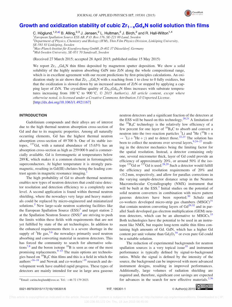
system, Figure 1 shows the calculated lattice parameters for
the cubic disordered solid solutions of Zr1�xGdxN from Ref.
50 together with the experimental curve, which is a combina-
tion of the relations between the Zr and Gd metals obtained
from RBS and the lattice parameters calculated from XRD
data. The measured lattice parameters follow the same
increasing trend with increasing GdN content as the calcula-
tions. The calculated lattice parameters slightly overestimate
our measured values, which is the usual condition found for
calculations employing the generalized gradient approxima-
tion for exchange-correlation effects in nitrides.57,59
However, this overestimation vanishes for the GdN rich
compositions. In Ref. 50, it was shown that the theoretical
overestimation for pure GdN with respect to experiments is
smaller compared to the case of pure ZrN. One should also
keep in mind that the calculations were done for the ideal
nitrogen stoichiometry while a slight understoichiometry is
found in our measurements (see below). The effect of such
understoichiometry on the lattice spacing can be different in
different nitrides, possibly adding to the slight differences in
slope between theory and experimental curves in Figure 1.
However, the gradual increase in lattice spacing with compo-
sition almost follows Vegard’s rule60 and the theoretical pre-
dictions and therefore it is a strong evidence of the formation
of solid solutions over the full compositional range.
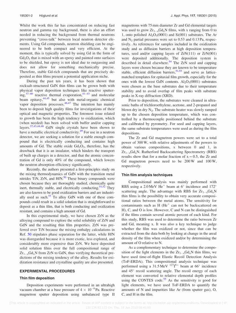
To determine the most favorable substrate temperature
for high quality epitaxial Zr1�xGdxN films, Zr0.5Gd0.5N was
deposited with a ZrN seed and capping layer onto
Al2O3(0001) at substrate temperatures between 100 and
900 �C. As seen in the different XRD scans in Figure 2, it is
mainly the orientation of the ZrN that determines the orienta-
tion of the Zr0.5Gd0.5N. The preferred growth orientation for
the highest (900 �C) and lowest (100 �C) applied tempera-
tures is h111i, while temperatures between 300 and 700 �Callow for a mixture of h111i and h001i oriented growth. No
other growth orientations were seen in longer overview
scans. While the hexagonal symmetry of the Al2O3(0001)
substrate surface will favor h111i oriented nucleation at high
temperatures, the in-plane lattice mismatch of Al2O3(0001)
compared to ZrN(111) is as large as 19.4%, which reduces
the possibility of forming continuous epitaxial layers, in par-
ticular, at limited growth temperatures. On the other hand,
Petrov and co-workers have previously shown that increased
adatom mobility, as induced by increased substrate tempera-
ture, generally promotes a h001i preferred growth orienta-
tion.61 Thus, the mixture of ZrN h111i and h001i oriented
growth at intermediate growth temperatures may be
explained by a competition between the driving forces for
h111i oriented epitaxy and for h001i oriented growth due to
FIG. 1. Measured (this work) and calculated (Ref. 50) lattice parameters for
the cubic rocksalt solid solution of Zr1�xGdxN with 0� x� 1.
FIG. 2. XRD data from (111) and (001) oriented Zr0.5Gd0.5N films on
Al2O3(0001) and (111) and (001) oriented ZrN seed and capping layers
grown at substrate temperatures between 100 and 900 �C.
195301-3 H€oglund et al. J. Appl. Phys. 117, 195301 (2015)
[This article is copyrighted as indicated in the article. Reuse of AIP content is subject to the terms at: http://scitation.aip.org/termsconditions. Downloaded to ] IP:
130.236.83.172 On: Thu, 18 Jun 2015 08:45:00
increased adatom mobility. At the highest temperature
though, the h111i oriented preferred growth indicates that
the interaction with the substrate becomes the determining
factor. An additional observation is the shift of the
Zr0.5Gd0.5N 111 peak towards higher angles, meaning
smaller out-of-plane lattice parameter, with increasing tem-
perature. This behavior is consistent with an increasing influ-
ence by the substrate surface lattice as the temperature is
increases, as evidenced by the trend towards h111i oriented
growth. Also a nitrogen under-stoichiometry, as is often
observed for reactively grown transition metal nitrides, may
have a similar influence on the lattice parameter evolution.
While it is beyond the scope of this work to clarify the rea-
son for this temperature effect, we note that the coefficients
of thermal expansion (CTE) of most transition metal nitrides
(e.g., CTEZrN¼ 7–9 �10�6 K�1) and sapphire perpendicular
to the C-plane (CTEAl2O3¼ 7–10 �10�6 K�1) are very simi-
lar and cannot explain the large observed peak shifts.
The XRD data for the intermediate growth temperature
500 �C, which exhibits the highest 002 peak intensity,
exhibits an inconsistency in the Zr0.5Gd0.5N 002 peak shift
direction. We find this interesting, as it is an indication of a
material with anisotropic mechanical and/or structural prop-
erties, as might be for the case in Ref. 50 predicted ordered
structure of ZrGdN2. Nevertheless, the formation of that
phase could not be found in any of the measured XRD
scans or X-ray pole figures (not shown), even though the
compositional ratios were correct and the in-plane lattice
mismatch was expected to be only 3.9% according to the
calculated lattice parameters in Ref. 50. Instead, the substi-
tutionally disordered Zr0.5Gd0.5N solid solution was
observed for all applied substrate temperatures. It was noted
in Ref. 50 that the predicted critical ordering temperature,
Tc¼ 1020 K (747 �C), is in the same range as where bulk
diffusion becomes extremely slow in nitrides.55 Since sev-
eral of our samples were grown at lower temperatures, the
absence of an ordered phase illustrates that surface diffusion
alone, which is active at all the considered temperatures, is
insufficient to create a long-range metal-site ordering in this
nitride system.
ToF-ERDA depth profiles were recorded for films that,
according to RBS, contain x¼ 0.30 in Zr1�xGdxN, both with
and without ZrN capping layers. Both films show composi-
tional levels of H, C, F, and Ar below the ToF-ERDA detec-
tion limit of 0.03 at. %. The level of O is also close to the
detection limit in the film that was covered with a capping
layer, while the film without a capping layer shows higher O
levels close to the surface. This indicates that the films do
not contain any O before they are exposed to air and start to
oxidize. It also shows that the sputtering targets are pure and
the vacuum conditions good enough to provide films without
contaminations. We further conclude that no Ar has been
incorporated during the sputter deposition. The N content in
the as-deposited films has been determined by combining
ToF-ERDA and RBS results and is found to be in the region
of 45–50 at. %.
A ToF-SIMS depth profile of a typical GdN film sand-
wiched between seed and capping layer of ZrN was recorded
and an important result for future neutron detector applications
is that the natural abundance of the five most common isotopes
in Gd, 155Gd¼ 14.8%, 156Gd¼ 20.6%, 157Gd¼ 15.7%, 158Gd
¼ 24.8%, and 160Gd¼ 21.8% could be confirmed.
To follow the oxidization of pure GdN without capping
layer, �400 nm of GdN was deposited onto an Al2O3 sub-
strate and then exposed to air at room temperature. The oxi-
dation was followed by the surface color change, recorded
every 4 s with a digital camera. The continuous oxidation
process is illustrated by a selection of these images of GdN
films on transparent Al2O3, exposed to air up to 19 h as
shown in Figure 3. The as-deposited sample had a silver-
metallic color that within the first minutes changed to be
more golden and then brownish. The rapid color change indi-
cates that the oxidization starts immediately. After the brown
appearance and within the first hour, all the colors of the
rainbow brightly appeared after each other. During the fol-
lowing few hours, the film appeared to be purple and green
with some interference color gradients indicating a slight
thickness gradient of the oxide and remaining film. After less
than 19 h, the film has become fully transparent and is com-
pletely oxidized. RBS measurements on a completely oxi-
dized film show that the majority of N has been replaced by
O. A similar but much faster color change, probably due to a
GdN film thicknesses of only �100 nm, has been reported in
Ref. 41.
To investigate the oxidization stability of Zr1�xGdxN, a
series of films with 0� x� 1 were deposited with and with-
out ZrN capping layers onto Si and Al2O3 substrates at
400 �C. These films were measured with RBS within two
weeks after they were deposited. A second measurement was
done 3–4 months after deposition, for those films that were
not fully oxidized already in the first measurement. All sam-
ples were stored in room temperature and in air. The results
are presented in Figure 4 and show that films with a high
amount of GdN oxidize within a very short time. Increasing
the amount of ZrN significantly slows down the oxidization
and films with x� 0.3 were just slightly oxidized even after
several months. The idea to alloy GdN with a chemically
more stable transition metal nitride with the purpose to pre-
vent it from oxidization is thus working, although oxidation
can not fully be avoided even with GdN contents as low as
x¼ 0.2.
FIG. 3. Color change for a GdN thin film on Al2O3 substrate during expo-
sure to air for up to 19 h.
195301-4 H€oglund et al. J. Appl. Phys. 117, 195301 (2015)
[This article is copyrighted as indicated in the article. Reuse of AIP content is subject to the terms at: http://scitation.aip.org/termsconditions. Downloaded to ] IP:
130.236.83.172 On: Thu, 18 Jun 2015 08:45:00
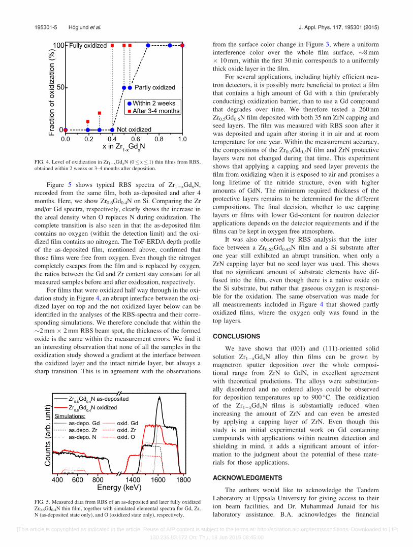
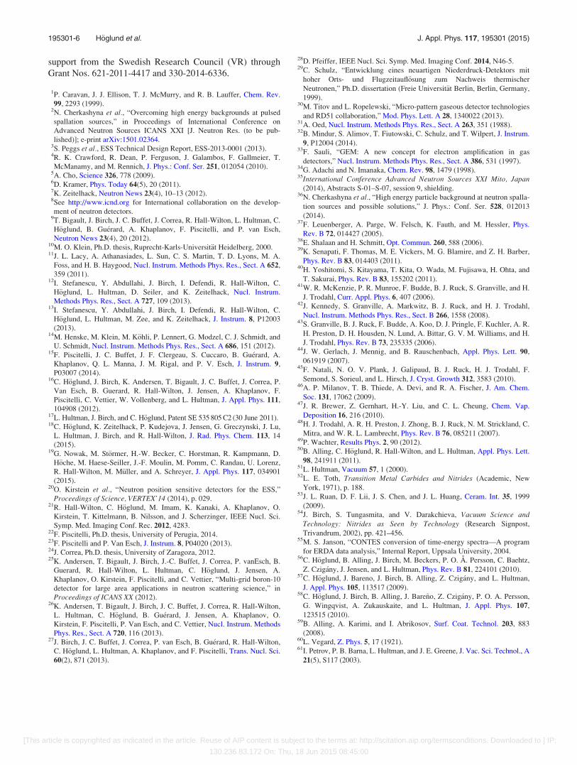
Figure 5 shows typical RBS spectra of Zr1�xGdxN,
recorded from the same film, both as-deposited and after 4
months. Here, we show Zr0.6Gd0.4N on Si. Comparing the Zr
and/or Gd spectra, respectively, clearly shows the increase in
the areal density when O replaces N during oxidization. The
complete transition is also seen in that the as-deposited film
contains no oxygen (within the detection limit) and the oxi-
dized film contains no nitrogen. The ToF-ERDA depth profile
of the as-deposited film, mentioned above, confirmed that
those films were free from oxygen. Even though the nitrogen
completely escapes from the film and is replaced by oxygen,
the ratios between the Gd and Zr content stay constant for all
measured samples before and after oxidization, respectively.
For films that were oxidized half way through in the oxi-
dation study in Figure 4, an abrupt interface between the oxi-
dized layer on top and the not oxidized layer below can be
identified in the analyses of the RBS-spectra and their corre-
sponding simulations. We therefore conclude that within the
�2 mm � 2 mm RBS beam spot, the thickness of the formed
oxide is the same within the measurement errors. We find it
an interesting observation that none of all the samples in the
oxidization study showed a gradient at the interface between
the oxidized layer and the intact nitride layer, but always a
sharp transition. This is in agreement with the observations
from the surface color change in Figure 3, where a uniform
interference color over the whole film surface, �8 mm
� 10 mm, within the first 30 min corresponds to a uniformly
thick oxide layer in the film.
For several applications, including highly efficient neu-
tron detectors, it is possibly more beneficial to protect a film
that contains a high amount of Gd with a thin (preferably
conducting) oxidization barrier, than to use a Gd compound
that degrades over time. We therefore tested a 260 nm
Zr0.5Gd0.5N film deposited with both 35 nm ZrN capping and
seed layers. The film was measured with RBS soon after it
was deposited and again after storing it in air and at room
temperature for one year. Within the measurement accuracy,
the compositions of the Zr0.5Gd0.5N film and ZrN protective
layers were not changed during that time. This experiment
shows that applying a capping and seed layer prevents the
film from oxidizing when it is exposed to air and promises a
long lifetime of the nitride structure, even with higher
amounts of GdN. The minimum required thickness of the
protective layers remains to be determined for the different
compositions. The final decision, whether to use capping
layers or films with lower Gd-content for neutron detector
applications depends on the detector requirements and if the
films can be kept in oxygen free atmosphere.
It was also observed by RBS analysis that the inter-
face between a Zr0.55Gd0.45N film and a Si substrate after
one year still exhibited an abrupt transition, when only a
ZrN capping layer but no seed layer was used. This shows
that no significant amount of substrate elements have dif-
fused into the film, even though there is a native oxide on
the Si substrate, but rather that gaseous oxygen is responsi-
ble for the oxidation. The same observation was made for
all measurements included in Figure 4 that showed partly
oxidized films, where the oxygen only was found in the
top layers.
CONCLUSIONS
We have shown that (001) and (111)-oriented solid
solution Zr1�xGdxN alloy thin films can be grown by
magnetron sputter deposition over the whole composi-
tional range from ZrN to GdN, in excellent agreement
with theoretical predictions. The alloys were substitution-
ally disordered and no ordered alloys could be observed
for deposition temperatures up to 900 �C. The oxidization
of the Zr1�xGdxN films is substantially reduced when
increasing the amount of ZrN and can even be arrested
by applying a capping layer of ZrN. Even though this
study is an initial experimental work on Gd containing
compounds with applications within neutron detection and
shielding in mind, it adds a significant amount of infor-
mation to the judgment about the potential of these mate-
rials for those applications.
ACKNOWLEDGMENTS
The authors would like to acknowledge the Tandem
Laboratory at Uppsala University for giving access to their
ion beam facilities, and Dr. Muhammad Junaid for his
laboratory assistance. B.A. acknowledges the financial
FIG. 4. Level of oxidization in Zr1�xGdxN (0� x� 1) thin films from RBS,
obtained within 2 weeks or 3–4 months after deposition.
FIG. 5. Measured data from RBS of an as-deposited and later fully oxidized
Zr0.6Gd0.4N thin film, together with simulated elemental spectra for Gd, Zr,
N (as-deposited state only), and O (oxidized state only), respectively.
195301-5 H€oglund et al. J. Appl. Phys. 117, 195301 (2015)
[This article is copyrighted as indicated in the article. Reuse of AIP content is subject to the terms at: http://scitation.aip.org/termsconditions. Downloaded to ] IP:
130.236.83.172 On: Thu, 18 Jun 2015 08:45:00
support from the Swedish Research Council (VR) through
Grant Nos. 621-2011-4417 and 330-2014-6336.
1P. Caravan, J. J. Ellison, T. J. McMurry, and R. B. Lauffer, Chem. Rev.
99, 2293 (1999).2N. Cherkashyna et al., “Overcoming high energy backgrounds at pulsed
spallation sources,” in Proceedings of International Conference on
Advanced Neutron Sources ICANS XXI [J. Neutron Res. (to be pub-
lished)]; e-print arXiv:1501.02364.3S. Peggs et al., ESS Technical Design Report, ESS-2013-0001 (2013).4R. K. Crawford, R. Dean, P. Ferguson, J. Galambos, F. Gallmeier, T.
McManamy, and M. Rennich, J. Phys.: Conf. Ser. 251, 012054 (2010).5A. Cho, Science 326, 778 (2009).6D. Kramer, Phys. Today 64(5), 20 (2011).7K. Zeitelhack, Neutron News 23(4), 10–13 (2012).8See http://www.icnd.org for International collaboration on the develop-
ment of neutron detectors.9T. Bigault, J. Birch, J. C. Buffet, J. Correa, R. Hall-Wilton, L. Hultman, C.
H€oglund, B. Gu�erard, A. Khaplanov, F. Piscitelli, and P. van Esch,
Neutron News 23(4), 20 (2012).10M. O. Klein, Ph.D. thesis, Ruprecht-Karls-Universit€at Heidelberg, 2000.11J. L. Lacy, A. Athanasiades, L. Sun, C. S. Martin, T. D. Lyons, M. A.
Foss, and H. B. Haygood, Nucl. Instrum. Methods Phys. Res., Sect. A 652,
359 (2011).12I. Stefanescu, Y. Abdullahi, J. Birch, I. Defendi, R. Hall-Wilton, C.
H€oglund, L. Hultman, D. Seiler, and K. Zeitelhack, Nucl. Instrum.
Methods Phys. Res., Sect. A 727, 109 (2013).13I. Stefanescu, Y. Abdullahi, J. Birch, I. Defendi, R. Hall-Wilton, C.
H€oglund, L. Hultman, M. Zee, and K. Zeitelhack, J. Instrum. 8, P12003
(2013).14M. Henske, M. Klein, M. K€ohli, P. Lennert, G. Modzel, C. J. Schmidt, and
U. Schmidt, Nucl. Instrum. Methods Phys. Res., Sect. A 686, 151 (2012).15F. Piscitelli, J. C. Buffet, J. F. Clergeau, S. Cuccaro, B. Gu�erard, A.
Khaplanov, Q. L. Manna, J. M. Rigal, and P. V. Esch, J. Instrum. 9,
P03007 (2014).16C. H€oglund, J. Birch, K. Andersen, T. Bigault, J. C. Buffet, J. Correa, P.
Van Esch, B. Guerard, R. Hall-Wilton, J. Jensen, A. Khaplanov, F.
Piscitelli, C. Vettier, W. Vollenberg, and L. Hultman, J. Appl. Phys. 111,
104908 (2012).17L. Hultman, J. Birch, and C. H€oglund, Patent SE 535 805 C2 (30 June 2011).18C. H€oglund, K. Zeitelhack, P. Kudejova, J. Jensen, G. Greczynski, J. Lu,
L. Hultman, J. Birch, and R. Hall-Wilton, J. Rad. Phys. Chem. 113, 14
(2015).19G. Nowak, M. St€ormer, H.-W. Becker, C. Horstman, R. Kampmann, D.
H€oche, M. Haese-Seiller, J.-F. Moulin, M. Pomm, C. Randau, U. Lorenz,
R. Hall-Wilton, M. M€uller, and A. Schreyer, J. Appl. Phys. 117, 034901
(2015).20O. Kirstein et al., “Neutron position sensitive detectors for the ESS,”
Proceedings of Science, VERTEX’14 (2014), p. 029.21R. Hall-Wilton, C. H€oglund, M. Imam, K. Kanaki, A. Khaplanov, O.
Kirstein, T. Kittelmann, B. Nilsson, and J. Scherzinger, IEEE Nucl. Sci.
Symp. Med. Imaging Conf. Rec. 2012, 4283.22F. Piscitelli, Ph.D. thesis, University of Perugia, 2014.23F. Piscitelli and P. Van Esch, J. Instrum. 8, P04020 (2013).24J. Correa, Ph.D. thesis, University of Zaragoza, 2012.25K. Andersen, T. Bigault, J. Birch, J.-C. Buffet, J. Correa, P. vanEsch, B.
Guerard, R. Hall-Wilton, L. Hultman, C. H€oglund, J. Jensen, A.
Khaplanov, O. Kirstein, F. Piscitelli, and C. Vettier, “Multi-grid boron-10
detector for large area applications in neutron scattering science,” in
Proceedings of ICANS XX (2012).26K. Andersen, T. Bigault, J. Birch, J. C. Buffet, J. Correa, R. Hall-Wilton,
L. Hultman, C. H€oglund, B. Gu�erard, J. Jensen, A. Khaplanov, O.
Kirstein, F. Piscitelli, P. Van Esch, and C. Vettier, Nucl. Instrum. Methods
Phys. Res., Sect. A 720, 116 (2013).27J. Birch, J. C. Buffet, J. Correa, P. van Esch, B. Gu�erard, R. Hall-Wilton,
C. H€oglund, L. Hultman, A. Khaplanov, and F. Piscitelli, Trans. Nucl. Sci.
60(2), 871 (2013).
28D. Pfeiffer, IEEE Nucl. Sci. Symp. Med. Imaging Conf. 2014, N46-5.29C. Schulz, “Entwicklung eines neuartigen Niederdruck-Detektors mit
hoher Orts- und Flugzeitaufl€osung zum Nachweis thermischer
Neutronen,” Ph.D. dissertation (Freie Universit€at Berlin, Berlin, Germany,
1999).30M. Titov and L. Ropelewski, “Micro-pattern gaseous detector technologies
and RD51 collaboration,” Mod. Phys. Lett. A 28, 1340022 (2013).31A. Oed, Nucl. Instrum. Methods Phys. Res., Sect. A 263, 351 (1988).32B. Mindur, S. Alimov, T. Fiutowski, C. Schulz, and T. Wilpert, J. Instrum.
9, P12004 (2014).33F. Sauli, “GEM: A new concept for electron amplification in gas
detectors,” Nucl. Instrum. Methods Phys. Res., Sect. A 386, 531 (1997).34G. Adachi and N. Imanaka, Chem. Rev. 98, 1479 (1998).35International Conference Advanced Neutron Sources XXI Mito, Japan
(2014), Abstracts S-01–S-07, session 9, shielding.36N. Cherkashyna et al., “High energy particle background at neutron spalla-
tion sources and possible solutions,” J. Phys.: Conf. Ser. 528, 012013
(2014).37F. Leuenberger, A. Parge, W. Felsch, K. Fauth, and M. Hessler, Phys.
Rev. B 72, 014427 (2005).38E. Shalaan and H. Schmitt, Opt. Commun. 260, 588 (2006).39K. Senapati, F. Thomas, M. E. Vickers, M. G. Blamire, and Z. H. Barber,
Phys. Rev. B 83, 014403 (2011).40H. Yoshitomi, S. Kitayama, T. Kita, O. Wada, M. Fujisawa, H. Ohta, and
T. Sakurai, Phys. Rev. B 83, 155202 (2011).41W. R. McKenzie, P. R. Munroe, F. Budde, B. J. Ruck, S. Granville, and H.
J. Trodahl, Curr. Appl. Phys. 6, 407 (2006).42J. Kennedy, S. Granville, A. Markwitz, B. J. Ruck, and H. J. Trodahl,
Nucl. Instrum. Methods Phys. Res., Sect. B 266, 1558 (2008).43S. Granville, B. J. Ruck, F. Budde, A. Koo, D. J. Pringle, F. Kuchler, A. R.
H. Preston, D. H. Housden, N. Lund, A. Bittar, G. V. M. Williams, and H.
J. Trodahl, Phys. Rev. B 73, 235335 (2006).44J. W. Gerlach, J. Mennig, and B. Rauschenbach, Appl. Phys. Lett. 90,
061919 (2007).45F. Natali, N. O. V. Plank, J. Galipaud, B. J. Ruck, H. J. Trodahl, F.
Semond, S. Sorieul, and L. Hirsch, J. Cryst. Growth 312, 3583 (2010).46A. P. Milanov, T. B. Thiede, A. Devi, and R. A. Fischer, J. Am. Chem.
Soc. 131, 17062 (2009).47J. R. Brewer, Z. Gernhart, H.-Y. Liu, and C. L. Cheung, Chem. Vap.
Deposition 16, 216 (2010).48H. J. Trodahl, A. R. H. Preston, J. Zhong, B. J. Ruck, N. M. Strickland, C.
Mitra, and W. R. L. Lambrecht, Phys. Rev. B 76, 085211 (2007).49P. Wachter, Results Phys. 2, 90 (2012).50B. Alling, C. H€oglund, R. Hall-Wilton, and L. Hultman, Appl. Phys. Lett.
98, 241911 (2011).51L. Hultman, Vacuum 57, 1 (2000).52L. E. Toth, Transition Metal Carbides and Nitrides (Academic, New
York, 1971), p. 188.53J. L. Ruan, D. F. Lii, J. S. Chen, and J. L. Huang, Ceram. Int. 35, 1999
(2009).54J. Birch, S. Tungasmita, and V. Darakchieva, Vacuum Science and
Technology: Nitrides as Seen by Technology (Research Signpost,
Trivandrum, 2002), pp. 421–456.55M. S. Janson, “CONTES conversion of time-energy spectra—A program
for ERDA data analysis,” Internal Report, Uppsala University, 2004.56C. H€oglund, B. Alling, J. Birch, M. Beckers, P. O. A. Persson, C. Baehtz,
Z. Czig�any, J. Jensen, and L. Hultman, Phys. Rev. B 81, 224101 (2010).57C. H€oglund, J. Bareno, J. Birch, B. Alling, Z. Czig�any, and L. Hultman,
J. Appl. Phys. 105, 113517 (2009).58C. H€oglund, J. Birch, B. Alling, J. Bare~no, Z. Czig�any, P. O. A. Persson,
G. Wingqvist, A. Zukauskaite, and L. Hultman, J. Appl. Phys. 107,
123515 (2010).59B. Alling, A. Karimi, and I. Abrikosov, Surf. Coat. Technol. 203, 883
(2008).60L. Vegard, Z. Phys. 5, 17 (1921).61I. Petrov, P. B. Barna, L. Hultman, and J. E. Greene, J. Vac. Sci. Technol., A
21(5), S117 (2003).
195301-6 H€oglund et al. J. Appl. Phys. 117, 195301 (2015)
[This article is copyrighted as indicated in the article. Reuse of AIP content is subject to the terms at: http://scitation.aip.org/termsconditions. Downloaded to ] IP:
130.236.83.172 On: Thu, 18 Jun 2015 08:45:00