Embed Size (px)
Citation preview
I
Zinc Oxide Nanostructures Synthesized by
Oxidization of Zinc
A THESIS SUBMITTED IN PARTIAL FULFILLMENT OF THE
REQUIREMENTS FOR THE DEGREE OF
Bachelor of Technology
In
Metallurgical & Materials Engineering
By
MANISH KUMAR (10604026)
SHAKTI SWARUP SAHU (10604041)
Department of Metallurgical & Materials Engineering
National Institute of Technology
Rourkela
2010
II
Zinc Oxide Nanostructures Synthesized by
Oxidization of Zinc
A THESIS SUBMITTED IN PARTIAL FULFILLMENT OF THE
REQUIREMENTS FOR THE DEGREE OF
Bachelor of Technology
In
Metallurgical & Materials Engineering
By
MANISH KUMAR (10604026)
SHAKTI SWARUP SAHU (10604041)
Under the Guidance of
Prof. S. N. Alam
Department of Metallurgical & Materials Engineering
National Institute of Technology
Rourkela
2010
III
National Institute of Technology
Rourkela
Certificate
This is to certify that the thesis entitled, “Zinc Oxide Nanostructures Synthesized by Oxidation of
Zinc” submitted by Manish Kumar (10604026) and Shakti Swarup Sahu (10604041) in partial
fulfillment of the requirements for the award of Bachelor of Technology Degree in Metallurgical &
Materials Engineering to the National Institute Of Technology, Rourkela (Deemed University) is an
authentic work carried out by them under my supervision and guidance. To the best of my knowledge,
the matter embodied in the thesis has not been submitted to any other University/Institute for the award
of any Degree or Diploma.
S. N. Alam Date:
Assistant Professor
Dept. of Metallurgical & Materials Engineering,
National Institute of Technology, Rourkela
Rourkela, Orissa-769008.
IV
Acknowledgment
We welcome this opportunity to express our heartfelt gratitude and regards to our project guide
Prof. S. N. Alam, Department of Metallurgical & Materials Engineering, National Institute of
Technology, Rourkela for his superb guidance. We would like to thank him for assigning us the project
“Zinc Oxide Nanostructures Synthesized by Oxidation of Zinc”. Without his guidance and support we
would not have been able to take the necessary steps required for the completion of this phase of our
project. His motivation and help during the period of work has been invaluable in the completion of this
work. He always bestowed parental care upon us and evinced keen interest in solving our problems. An
erudite teacher, a magnificent person and a strict disciplinarian, we consider ourselves fortunate to have
worked under his supervision.
We wish to record our gratitude to our project coordinators Prof. A. K. Panda and Prof. M. Kumar
for helping us at each and every step in conducting this report. We would like to thank them for their
stimulating and innovative ideas for implementing this project. We would also like to express our sincere
gratitude towards our Head of the Department, Prof. B. B.Verma. We are highly grateful to Prof. B. B.
Verma, Head of the department, Metallurgical & Materials Engineering, NIT Rourkela, for providing
necessary facilities during the course of the work. We also take this opportunity to thank our parents and
family members for constantly supporting us and encouraging us during our study. We also would like to
thank all our friends for their help and support.
We are also thankful to Prof. D. Chaira for permitting us to access the SEM. We would like to
thank Mr. Rajesh Patnayak for helping us in analyzing the samples in SEM. We would like to thank Mr.
Uday Sahu for helping in carrying out the x-ray analysis of our samples. We would also like to thank Mr.
S. Hembram and all other staff of the heat treatment lab of our department in helping us during heat
treatment of the samples. We wish to place our deep sense of thanks to all who are directly or indirectly
associated with our project for their cooperation and critical suggestions during our experimental work.
Manish Kumar (10604026) Date:
Shakti Swarup Sahu (10604041)

V
CONTENTS
ABSTRACT .…………………………………………………………. 1
CHAPTER-1: INTRODUCTION
1.0 Introduction ……………………………………………………. 2
CHAPTER-2: LITERATURE SURVEY
2. 1 Properties of Zinc Oxide ……………………………………… 5
2.1.1 Physical properties 5
2.1.2 Electrical properties 7
2.1.3 Optical properties 8
2.2 Applications ……………………………………………………. 8
2.2.1 Rubber manufacture 8
2.2.2 Medical uses 9
2.2.3 Food additives 9
2.2.4 Anti-corrosive coatings 9
2.2.5 Electronic applications 9
2.3 Synthesis of ZnO ………………………………………………. 10
2.3.1 Proposed method for synthesis of ZnO 11
VI
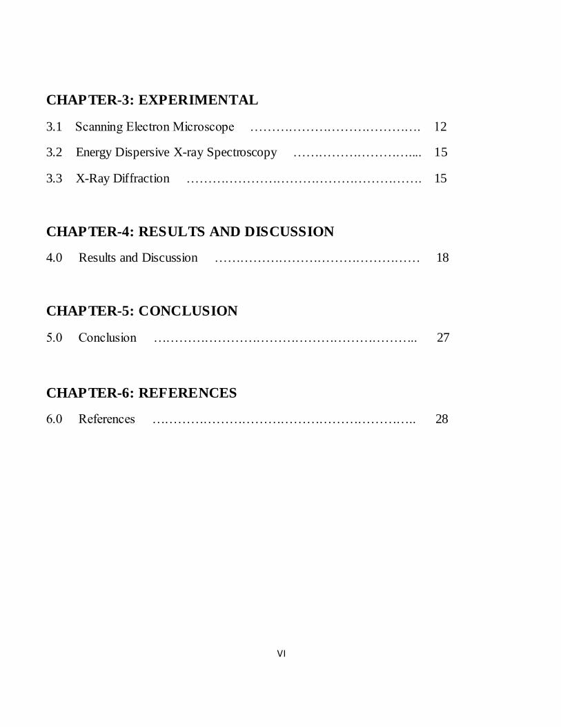
CHAPTER-3: EXPERIMENTAL
3.1 Scanning Electron Microscope …………………………………. 12
3.2 Energy Dispersive X-ray Spectroscopy ……………………….... 15
3.3 X-Ray Diffraction ………………………………………………. 15
CHAPTER-4: RESULTS AND DISCUSSION
4.0 Results and Discussion ………………………………………… 18
CHAPTER-5: CONCLUSION
5.0 Conclusion …………………………………………………….. 27
CHAPTER-6: REFERENCES
6.0 References …………………………………………………….. 28
1
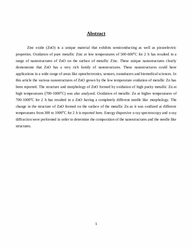
Abstract
Zinc oxide (ZnO) is a unique material that exhibits semiconducting as well as piezoelectric
properties. Oxidation of pure metallic Zinc at low temperatures of 500-600oC for 2 h has resulted in a
range of nanostructures of ZnO on the surface of metallic Zinc. These unique nanostructures clearly
demonstrate that ZnO has a very rich family of nanostructures. These nanostructures could have
applications in a wide range of areas like optoelectronics, sensors, transducers and biomedical sciences. In
this article the various nanostructures of ZnO grown by the low temperature oxidation of metallic Zn has
been reported. The structure and morphology of ZnO formed by oxidation of high purity metallic Zn at
high temperatures (700-1000oC) was also analyzed. Oxidation of metallic Zn at higher temperatures of
700-1000oC for 2 h has resulted in a ZnO having a completely different needle like morphology. The
change in the structure of ZnO formed on the surface of the metallic Zn as it was oxidized at different
temperatures from 300 to 1000oC for 2 h is reported here. Energy dispersive x-ray spectroscopy and x-ray
diffraction were performed in order to determine the composition of the nanostructures and the needle like
structures.
2
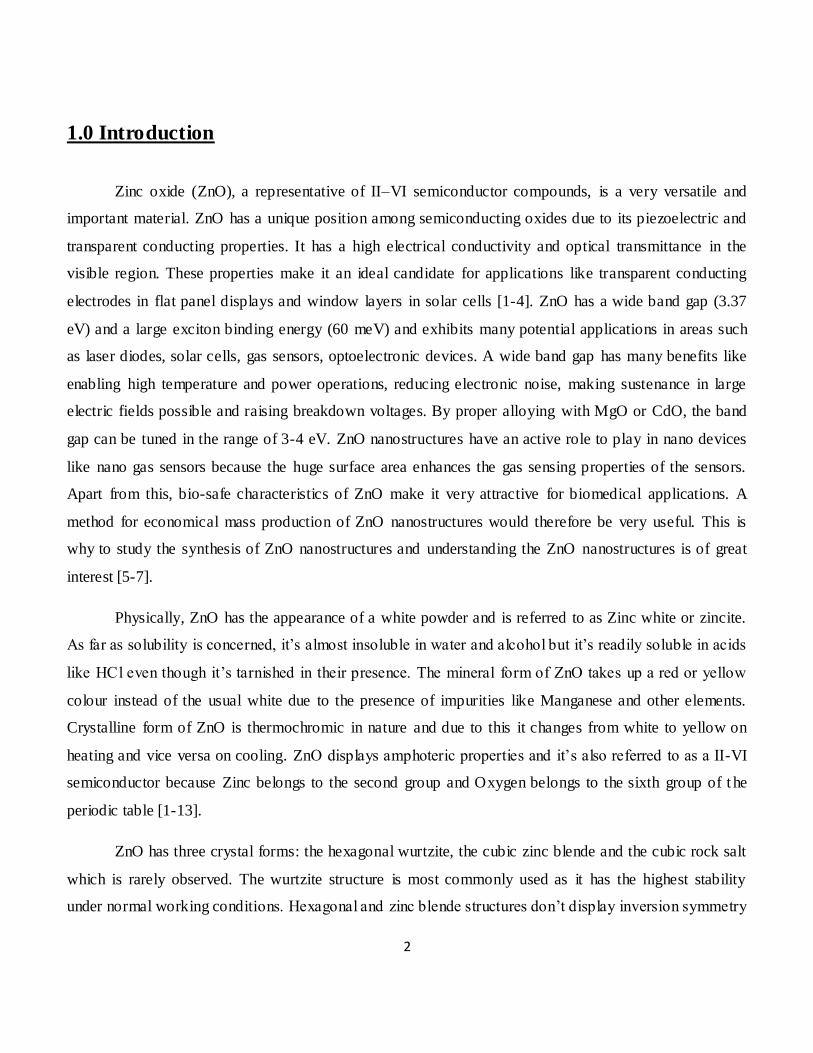
1.0 Introduction
Zinc oxide (ZnO), a representative of II–VI semiconductor compounds, is a very versatile and
important material. ZnO has a unique position among semiconducting oxides due to its piezoelectric and
transparent conducting properties. It has a high electrical conductivity and optical transmittance in the
visible region. These properties make it an ideal candidate for applications like transparent conducting
electrodes in flat panel displays and window layers in solar cells [1-4]. ZnO has a wide band gap (3.37
eV) and a large exciton binding energy (60 meV) and exhibits many potential applications in areas such
as laser diodes, solar cells, gas sensors, optoelectronic devices. A wide band gap has many benefits like
enabling high temperature and power operations, reducing electronic noise, making sustenance in large
electric fields possible and raising breakdown voltages. By proper alloying with MgO or CdO, the band
gap can be tuned in the range of 3-4 eV. ZnO nanostructures have an active role to play in nano devices
like nano gas sensors because the huge surface area enhances the gas sensing properties of the sensors.
Apart from this, bio-safe characteristics of ZnO make it very attractive for biomedical applications. A
method for economical mass production of ZnO nanostructures would therefore be very useful. This is
why to study the synthesis of ZnO nanostructures and understanding the ZnO nanostructures is of great
interest [5-7].
Physically, ZnO has the appearance of a white powder and is referred to as Zinc white or zincite.
As far as solubility is concerned, it‟s almost insoluble in water and alcohol but it‟s readily soluble in acids
like HCl even though it‟s tarnished in their presence. The mineral form of ZnO takes up a red or yellow
colour instead of the usual white due to the presence of impurities like Manganese and other elements.
Crystalline form of ZnO is thermochromic in nature and due to this it changes from white to yellow on
heating and vice versa on cooling. ZnO displays amphoteric properties and it‟s also referred to as a II-VI
semiconductor because Zinc belongs to the second group and Oxygen belongs to the sixth group of t he
periodic table [1-13].
ZnO has three crystal forms: the hexagonal wurtzite, the cubic zinc blende and the cubic rock salt
which is rarely observed. The wurtzite structure is most commonly used as it has the highest stability
under normal working conditions. Hexagonal and zinc blende structures don‟t display inversion symmetry
3
and it is properties like these that are responsible for the piezoelectricity and pyroelectricity of ZnO. ZnO
is considered to be a soft material with a reading of 4.5 on the Mohs hardness scale. Its elastic constants
are not that impressive but ZnO has got very good thermal properties like high melting point, high
thermal capacity and conductivity and a low coefficient of thermal expansion which makes it suitable for
use as a ceramic [1-17].
Recently, various synthesis techniques have been developed to fabricate ZnO nanocrystals with
different shapes, which include metal-catalyzed vapour- liquid-solid (VLS) growth, physical vapour
deposition (PVD), chemical vapour deposition (CVD), metal-organic vapour-phase epitaxy, metal-organic
CVD, template-assisted growth and oxidation method [8-10]. Many of these techniques however are
complicated needing a high temperature for synthesis and also have a long reaction time. Apart from this,
these techniques also utilize toxic components and require expensive experimental setup. The oxidation
method on the other hand is a simple low-cost technique and very commonly used for the synthesis of
ZnO nanostructures. ZnO nanostructures have been successfully synthesized by oxidizing Zn foils at
700°C in air without the presence of a catalyst and carrier gas [36]. Sekar and co-workers [9] reported that
ZnO nanowires were grown on Si (100) substrates by oxidation of metallic Zn powder at 600°C. The
synthesized ZnO materials have been found to have rod like, belt like, wire like and needle like
morphologies. This route for synthesis of ZnO is economical as it uses the oxygen from the air [14-17, 21,
25].
Here an economical and environment friendly route has been used for the synthesis of ZnO on Zn
substrate by oxidation of pure metallic Zn in a muffle furnace. Different morphologies of ZnO both
nanostructured and microstructured have been achieved by us by controlling the oxidation temperature
and the holding time. Nanostructures such as nanowires, nanorods, nanobelts and nanoneedles were seen
on the metallic Zn substrate.
4
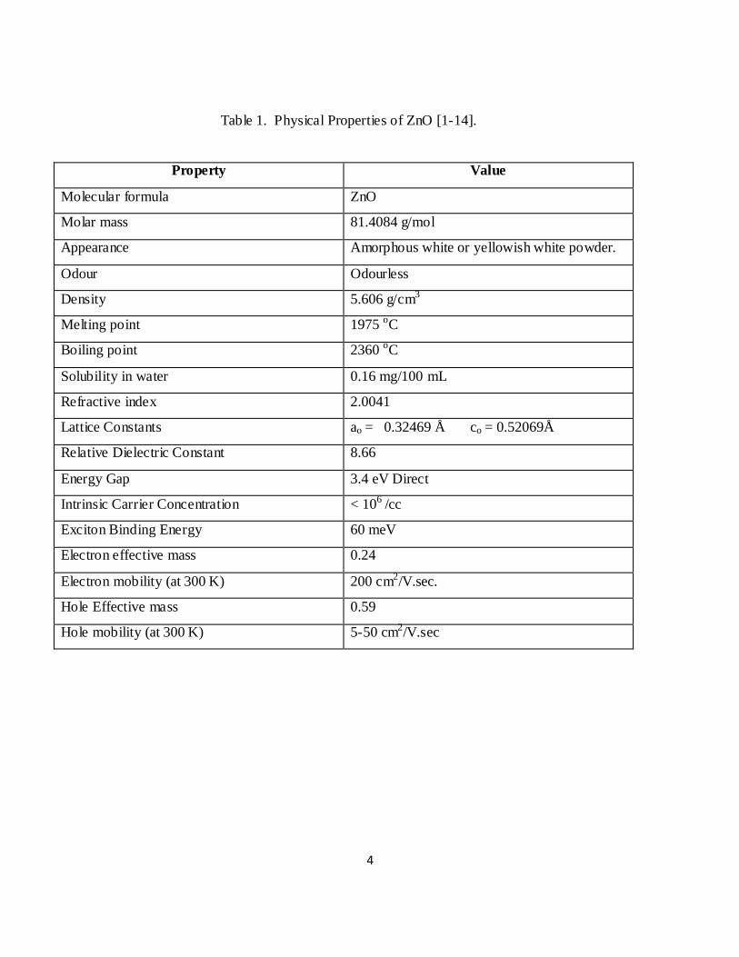
Table 1. Physical Properties of ZnO [1-14].
Property Value
Molecular formula ZnO
Molar mass 81.4084 g/mol
Appearance Amorphous white or yellowish white powder.
Odour Odourless
Density 5.606 g/cm3
Melting point 1975 oC
Boiling point 2360 oC
Solubility in water 0.16 mg/100 mL
Refractive index 2.0041
Lattice Constants ao = 0.32469 Å co = 0.52069Å
Relative Dielectric Constant 8.66
Energy Gap 3.4 eV Direct
Intrinsic Carrier Concentration < 106 /cc
Exciton Binding Energy 60 meV
Electron effective mass 0.24
Electron mobility (at 300 K) 200 cm2/V.sec.
Hole Effective mass 0.59
Hole mobility (at 300 K) 5-50 cm2/V.sec
5
2.0 Literature Survey
2.1 Properties of Zinc oxide
ZnO is a versatile material that exhibits semiconducting, piezoelectric as well as pyroelectric
properties. ZnO is a material that has a diverse range of nanostructures, whose configurations are far
richer than any other known nanomaterials including carbon nanotubes [2, 4, 6, 11].
2.1.1 Physical properties
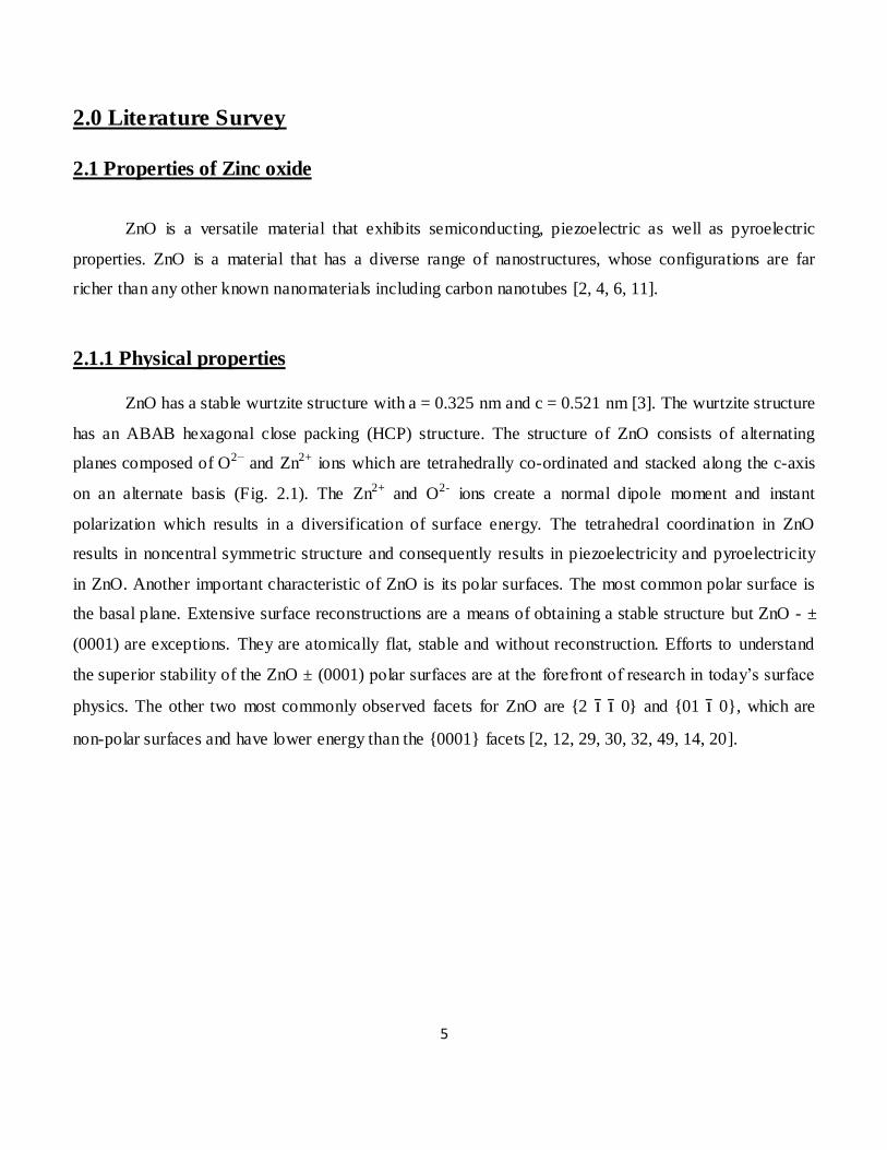
ZnO has a stable wurtzite structure with a = 0.325 nm and c = 0.521 nm [3]. The wurtzite structure
has an ABAB hexagonal close packing (HCP) structure. The structure of ZnO consists of alternating
planes composed of O2− and Zn2+ ions which are tetrahedrally co-ordinated and stacked along the c-axis
on an alternate basis (Fig. 2.1). The Zn2+ and O2- ions create a normal dipole moment and instant
polarization which results in a diversification of surface energy. The tetrahedral coordination in ZnO
results in noncentral symmetric structure and consequently results in piezoelectricity and pyroelectricity
in ZnO. Another important characteristic of ZnO is its polar surfaces. The most common polar surface is
the basal plane. Extensive surface reconstructions are a means of obtaining a stable structure but ZnO - ±
(0001) are exceptions. They are atomically flat, stable and without reconstruction. Efforts to understand
the superior stability of the ZnO ± (0001) polar surfaces are at the forefront of research in today‟s surface
physics. The other two most commonly observed facets for ZnO are {2 ī ī 0} and {01 ī 0}, which are
non-polar surfaces and have lower energy than the {0001} facets [2, 12, 29, 30, 32, 49, 14, 20].
6
Fig.2.1: Wurtzite structure of ZnO [2].
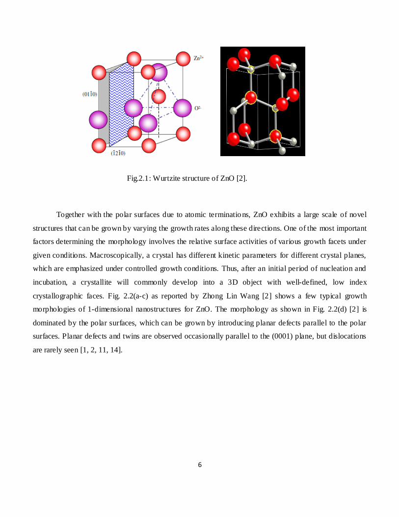
Together with the polar surfaces due to atomic terminations, ZnO exhibits a large scale of novel
structures that can be grown by varying the growth rates along these directions. One of the most important
factors determining the morphology involves the relative surface activities of various growth facets under
given conditions. Macroscopically, a crystal has different kinetic parameters for different crystal planes,
which are emphasized under controlled growth conditions. Thus, after an initial period of nucleation and
incubation, a crystallite will commonly develop into a 3D object with well-defined, low index
crystallographic faces. Fig. 2.2(a-c) as reported by Zhong Lin Wang [2] shows a few typical growth
morphologies of 1-dimensional nanostructures for ZnO. The morphology as shown in Fig. 2.2(d) [2] is
dominated by the polar surfaces, which can be grown by introducing planar defects parallel to the polar
surfaces. Planar defects and twins are observed occasionally parallel to the (0001) plane, but dislocations
are rarely seen [1, 2, 11, 14].
7
Fig. 2.2: Growth morphology of one dimensional ZnO nanostructures [2].
It is observed that when the dimensions of a semiconducting material keep decreasing i.e. from
macro to micro to nano scale, some of the physical properties of that material undergo changes. This
phenomenon is known as “quantum size effect” [4].
2.1.2 Electrical properties
Zinc oxide (ZnO) has a wide direct band gap (3.37 eV) and a relative large excitation binding
energy (60 meV). Owing to its unique properties wide band gap and large excitation binding energy, ZnO
has the potential to be applied chemical sensors, solar cells, luminescence devices etc. ZnO nanowires are
also reported to have behaved like a n-type semiconductor due to the presence of interstitial defects and
vacancies [4, 6, 11, 14, 20]. The major roadblock of ZnO for widespread applications in electronics and
photonics is its problems with p-type doping. Quite a few p-type doping efforts have been reported like
Ga and N co-doping method which resulted in the formation of low resistivity (0.5 Ω·cm) p-type ZnO thin
films. Successful p-type doping for ZnO nanostructures will give a boost to their future prospects in
nanoscale electronics and in the field of optoelectronics. P-type and n-type ZnO nanowires can serve as p-
n junction diodes and LEDs. Field effect transistors (FETs) fabricated from them can be used to make
complementary logic circuits [4, 20, 30, 32, 49, 50].
8
2.1.3 Optical Properties
Intrinsic optical properties of ZnO nanostructures are the focus of studies right now as they can be
used for implementing photonic devices. As a part of these studies, Photoluminescence (PL) spectra of
ZnO nanostructures have been widely reported. Excitonic emissions have been observed from the PL
spectra of ZnO nanorods. It is shown that if we confine the quantum size then it can greatly enhance the
exciton binding energy but an interesting observation is that the green emission intensity increases with a
decrease in the diameter of the nanowires. This is because of the larger surface-to-volume ratio of thinner
nanowires which favours a higher level of defects and surface recombination. Red luminescence band has
also been reported for which doubly ionized oxygen vacancies are considered responsible. Quantum
confinement was also observed to be responsible in causing a blue shift in the near UV emission peak in
the ZnO nanobelts. Some other fields of application include optical fibers, surface acoustic wave devices,
solar cells etc [4,8].
2.2 Applications
ZnO has got a wide array of applications. The reactivity of ZnO makes it ideal to be used as a
precursor for obtaining other compounds of Zn. ZnO has proved to be a boon for materials science as it
has got a combination of unique properties like UV absorption, anti microbial properties, s teady thermal
and optical properties. Be it ceramics, lubricants, ointments, adhesives or the rubber industry ZnO has got
a very significant contribution [39, 43-49].
2.2.1 Rubber manufacture
The rubber industry is responsible for consuming about 50% of the ZnO that‟s produced globally.
ZnO along with stearic acid are a must for activating the process of vulcanization in rubber manufacture.
Rubber curing becomes faster and more controlled when a combination of these two substances is used.
It‟s also a very important additive in car tyres. It helps in improving their thermal conductivity which
helps the tyres to dissipate heat quickly when they are in motion thereby increasing their life span [49].
9
2.2.2 Medical uses
A mixture of ZnO with 0.5% Fe2O3 is known as Calamine and is used in manufacturing Calamine
lotions. Fine particles of ZnO have anti microbial and deodorizing qualities and hence they are used for
packaging purposes. These properties along with its ability of neutralizing acids makes it ideal for use in
antiseptic creams, healing creams etc. they are also an important component of toothpastes and dental
prosthetics. Due to its ability to absorb ultraviolet light, ZnO is also used in sunscreens and sunblocks to
prevent sunburns. ZnO is also used in the making of cigarette filters as it helps in removing harmful
substances like H2S and HCN without affecting the flavour [49,50].
2.2.3 Food additives
ZnO is usually added to food products as a source of Zn which is considered to be a necessary
nutrient as it helps in the performance of various physiological activities like growth and proper
functioning of the sexual organs. ZnO is also added to fodder as a Zn supplement for livestock. Zinc
oxide is used to manufacture zinc gluconate which is nowadays found in cold prevention lozenges
[49,50].
2.2.4 Anti corrosive coatings
Zinc oxide is an excellent inhibitor of fungi, mildew and mould [50]. Paints which have ZnO are
usually used as anti corrosive coatings for various metals like galvanized Zn which is especially hard to
protect as it makes organic coatings brittle and unsuitable for adhesion [49]. ZnO paints on the other hand
maintain their flexibility and adhesive properties for years on end. The UV blocking abilities of ZnO also
play an important role in improving the resilience of the paint. Unlike some lead pigments that are
available commercially, ZnO is impervious to the effect of sulphur compounds that are present in the
atmosphere [43, 47].
2.2.5 Electronic applications
The wide band gap of ZnO enables it to be used for the purpose of making LEDs and laser diodes.
Transparent thin-film transistors (TTFT) can also be produced with ZnO. Nanorod sensors made of ZnO
are devices that detect fluctuations in electric current passing through the wires a s a result of the
10
adsorption of gas molecules. The nanorods can be made partial towards H2 gas by sputtering Pd clusters
on the surface which help in dissociating the H2 molecules thereby increasing the sensitivity of the
nanorods. H2 concentrations up to 10 ppm can be detected at room temperature without any response to
O2 [27,49].
Properties like biocompatibility have enabled ZnO to be used as a biomimic material to modify
and immobilize biomolecules. As Field-effect transistors (FETs), they can function without even a p-n
junction thus bypassing doping problems. This is why some FETs use nanorods made of ZnO as
conducting channels. ZnO is also used in making Zn-C dry cells, Ni-Cd oxide batteries, Zn-Ag oxide
batteries and also some secondary batteries. Another major area of ZnO application is fuel cell where it‟s
used to make various parts like the electrodes and sometimes also as the fuel. It can also act as a photo
catalyst in places like the solar cell [49, 50].
2.3 Synthesis
Keeping in view the extensive uses of ZnO, various types of synthesis techniques have been
formulated over the years. ZnO nanostructures can be synthesized by several methods such as sputtering
technique, vapour deposition, pulsed laser deposition (PLD), metal organic chemical vapour deposition
(MOCVD) and oxidation. Some other methods are vapour liquid-solid process and anodization.
Unfortunately, many of the stated techniques are problematic, needing high temperature for synthesis, and
having long reaction time, utilize toxic components and involve costly equipments. The oxidation method
is a simple, low-cost and most commonly used technique for the synthesis of ZnO nanostructures.
However, the deposition of zinc oxide by vapour deposition has seen increased research activity over the
past several years as the need for high quality zinc oxide thin films has increased. A key advantage of
chemical vapour deposition is its ability to easily incorporate dopants into films [17-26, 33-38].

11
2.3.1 Proposed Method for ZnO Synthesis
Keeping in view the various aspects of ZnO synthesis, we have reached the conclusion that the
simplest, cheapest and most effective way to synthesize ZnO is by oxidation method. Pure metallic Zn
was oxidized in air in a muffle furnace at various temperatures ranging from 300oC to 1000oC for 2 h and
the ZnO nanostructures and the microstructures formed on the Zn substrate were studied. The temperature
at which the ZnO structures changed from nano to micro was also tracked.
12
3.0 Experimental
Zn having purity 99.9 % was obtained from RFCL Limited (RANKEM), India. The oxidation of
metallic Zn was performed by heating the Zn at temperatures 300, 400, 500, 600, 700, 800, 900 and
1000°C for 2 h in a muffle furnace to obtain ZnO nanostructures on the surface of Zn. Zn was oxidized in
a silica crucible. The atmosphere in the muffle furnace used for oxidation was air. Oxygen present in air
was used for oxidizing Zn. The morphology of ZnO that was formed on metallic Zn was analyzed using a
JEOL JSM-6480LV scanning electron microscope (SEM). In order to identify the composition of the
nanostructures formed at lower oxidizing temperatures and the needle like structures formed at higher
oxidizing temperatures, energy dispersive x-ray spectroscopy (EDX) and x-ray diffraction (XRD) were
performed. The crystallographic structure of ZnO was analyzed with a Philips Pananalytical X' Pert x-ray
diffractometer using Cu Kα radiation (λ = 0.15406 nm). The JEOL JSM-6480LV scanning electron
microscope was attached with a high angle and ultra-thin window type energy dispersive x-ray
spectroscopy detector. An Oxford Instruments energy dispersive x-ray spectroscopy analyzer was
attached. An INCAPenta FET- X3 with a powerful Si (Li) detector having a 30 mm2 detecting crystal was
used.
3.1 Scanning Electron Microscope
The scanning electron microscope (SEM) is a type of electron microscope that helps in forming an
image of the sample surface by scanning. The electrons in the beam interact with the atoms in the surface
to generate signals that shed valuable light properties like composition, topography and electrical
conductivity. The so called „signals‟ produced by an SEM include secondary and back-scattered electrons,
characteristic x-rays, specimen current and light (due to cathodoluminescence). All SEMs usually have
the ability to detect secondary electrons but it‟s highly unlikely that a single SEM will have the ability to
detect all the signals mentioned above. SEM helps in obtaining high resolution images of specimens
ranging in size from those visible to the naked eye to those which are just a few nanometers in size
[28,41,43].
13
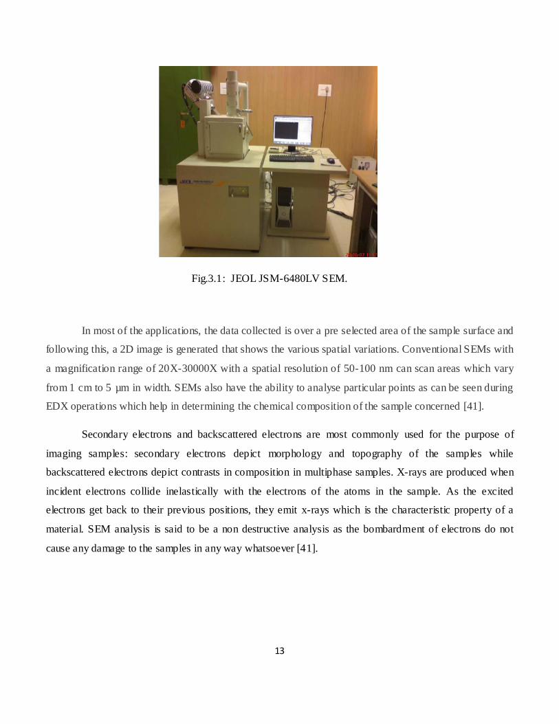
Fig.3.1: JEOL JSM-6480LV SEM.
In most of the applications, the data collected is over a pre selected area of the sample surface and
following this, a 2D image is generated that shows the various spatial variations. Conventional SEMs with
a magnification range of 20X-30000X with a spatial resolution of 50-100 nm can scan areas which vary
from 1 cm to 5 µm in width. SEMs also have the ability to analyse particular points as can be seen during
EDX operations which help in determining the chemical composition of the sample concerned [41].
Secondary electrons and backscattered electrons are most commonly used for the purpose of
imaging samples: secondary electrons depict morphology and topography of the samples while
backscattered electrons depict contrasts in composition in multiphase samples. X-rays are produced when
incident electrons collide inelastically with the electrons of the atoms in the sample. As the excited
electrons get back to their previous positions, they emit x-rays which is the characteristic property of a
material. SEM analysis is said to be a non destructive analysis as the bombardment of electrons do not
cause any damage to the samples in any way whatsoever [41].
14
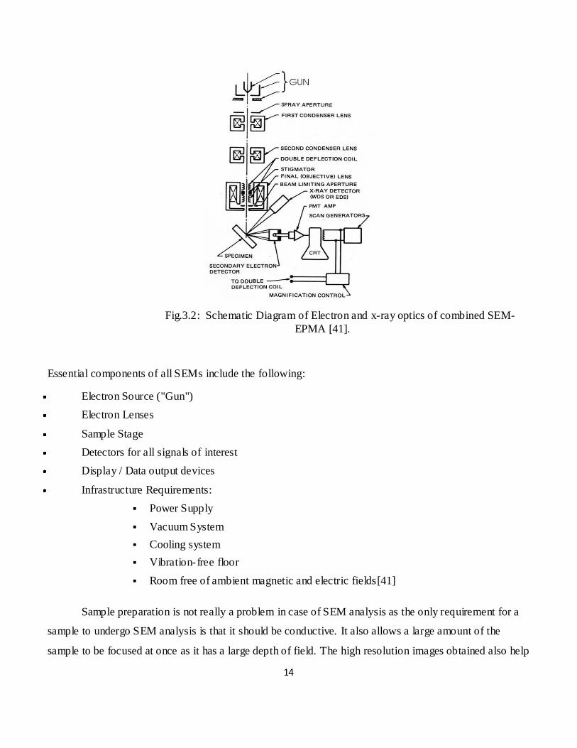
Fig.3.2: Schematic Diagram of Electron and x-ray optics of combined SEM-
EPMA [41].
Essential components of all SEMs include the following:
Electron Source ("Gun")
Electron Lenses
Sample Stage
Detectors for all signals of interest
Display / Data output devices
Infrastructure Requirements:
Power Supply
Vacuum System
Cooling system
Vibration-free floor
Room free of ambient magnetic and electric fields[41]
Sample preparation is not really a problem in case of SEM analysis as the only requirement for a
sample to undergo SEM analysis is that it should be conductive. It also allows a large amount of the
sample to be focused at once as it has a large depth of field. The high resolution images obtained also help
15
in analyzing the spatial features closely. A combination of all these features has made the SEM one of the
most popular instruments in the world on materials science [44].
3.2 Energy Dispersive X-Ray Spectroscopy
Energy dispersive x-ray analysis, also known as EDS, EDX or EDAX, is a technique used to
identify the elemental composition of a sample. During EDS, a sample is exposed to an electron beam
inside a scanning electron microscope (SEM). These electrons collide with the electrons within the
sample, causing some of them to be knocked out of their orbits. The vacated positions are filled by higher
energy electrons which emit x-rays in the process. By analyzing the emitted x-rays, the elemental
composition of the sample can be determined. EDS is a very handy tool for performing the constitutional
analysis of any kind of material [40].
3.3 X-Ray Diffraction
X-ray diffraction (XRD) is a non-destructive type of analytical technique which provides valuable
insight about the lattice structure of a crystalline substance like unit cell dimensions, bond angles etc.
XRD is based on the principle of constructive interference of x-rays and the sample concerned which
should be crystalline. The x-rays which are generated by a CRT are filtered, collimated and then directed
towards the sample. The interaction that follows produces constructive interference based on Bragg‟s law
which relates wavelength of the incident radiations to the diffraction angle and lattice spacing. The x-rays
that are obtained on diffraction are counted after proper processing. By altering the various parameters
like the geometry of incident rays and the orientation of the detector and crystal, we obtain all possible
diffraction directions of the lattice [31, 42].
16
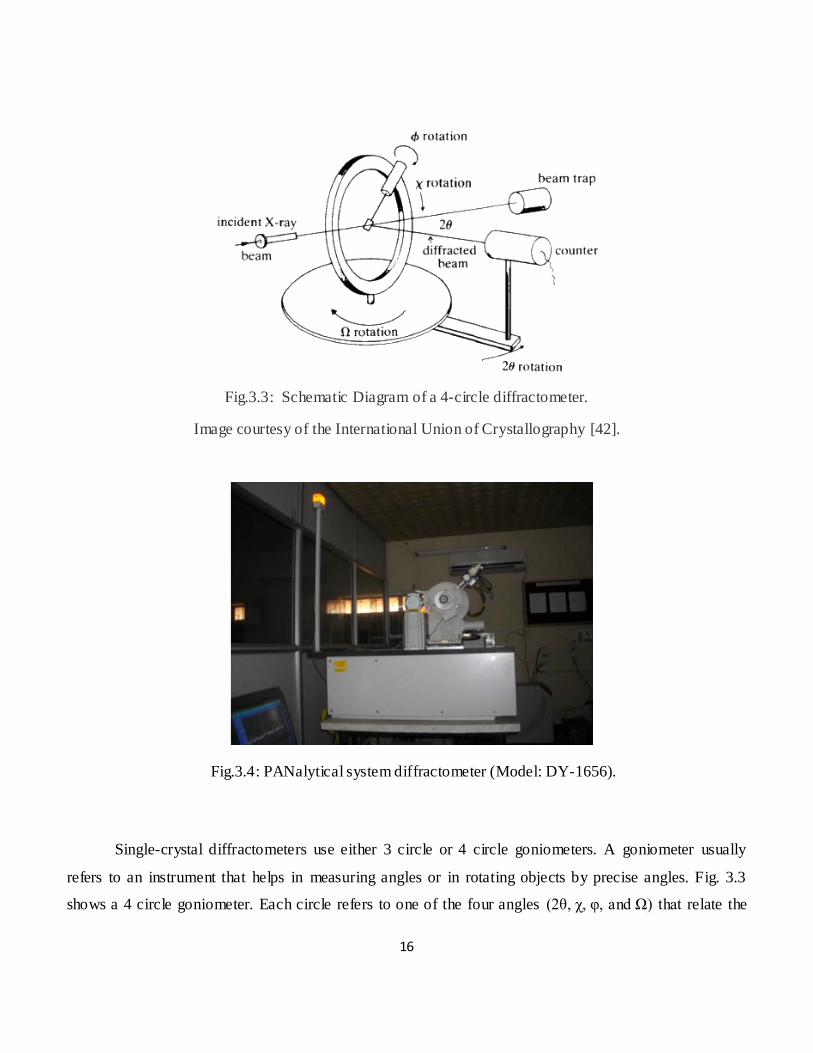
Fig.3.3: Schematic Diagram of a 4-circle diffractometer.
Image courtesy of the International Union of Crystallography [42].
Fig.3.4: PANalytical system diffractometer (Model: DY-1656).
Single-crystal diffractometers use either 3 circle or 4 circle goniometers. A goniometer usually
refers to an instrument that helps in measuring angles or in rotating objects by precise angles. Fig. 3.3
shows a 4 circle goniometer. Each circle refers to one of the four angles (2θ, χ, φ, and Ω) that relate the

17
incident ray, crystal lattice and the detector to each other. Samples are first attached to brass pins. Then
they are set up on the goniometer heads. By adjusting the X, Y and Z orthogonal directions we can adjust
the centering of the crystal within the x-ray beam [42].
18
4.0 Results and Discussion
Nanostructures have attracted attention of researchers for their many important technological
applications. The synthesis of nanostructures is a growing area of research. The synthesis of
nanostructures by a low cost process would be of great technological importance. The ZnO nanostructures
were synthesized by oxidizing pure metallic Zn. Pure metallic Zinc was heated at various temperatures
ranging from 300 to 1000°C for 2 h. It should be noted that Zinc has a melting point of 419.5°C whereas
its boiling point is 907°C. The choice of the range of oxidizing temperature was made in order to find out
the change in the morphology of ZnO that was formed on Zn substrate. The aim was to track the change
in morphology from nanostructured ZnO to microstructured ZnO as the oxidation temperature was
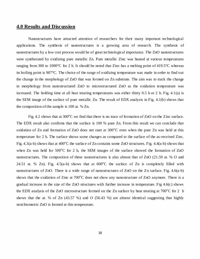
increased. The holding time at all heat treating temperatures was either thirty 0.5 h or 2 h. Fig. 4.1(a) is
the SEM image of the surface of pure metallic Zn. The result of EDX analysis in Fig. 4.1(b) shows that
the composition of the sample is 100 at. % Zn.
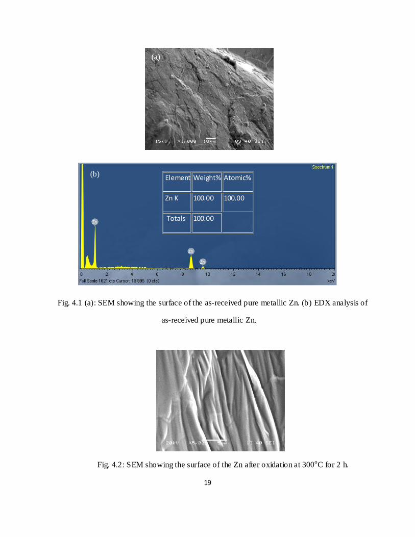
Fig. 4.2 shows that at 300oC we find that there is no trace of formation of ZnO on the Zinc surface.
The EDX result also confirms that the surface is 100 % pure Zn. From this result we can conclude that
oxidation of Zn and formation of ZnO does not start at 300oC even when the pure Zn was held at this
temperature for 2 h. The surface shows some changes as compared to the surface of the as-received Zinc.
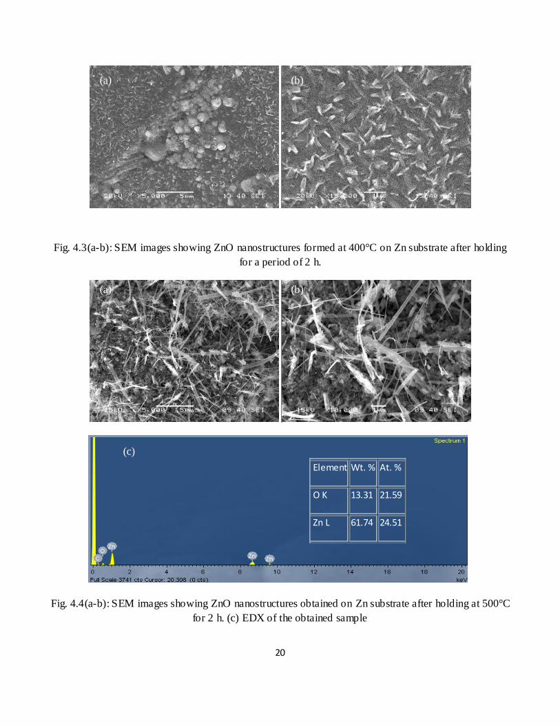
Fig. 4.3(a-b) shows that at 400oC the surface of Zn contains some ZnO structures. Fig. 4.4(a-b) shows that
when Zn was held for 500oC for 2 h, the SEM images of the surface showed the formation of ZnO
nanostructures. The composition of these nanostructures is also almost that of ZnO (21.59 at. % O and
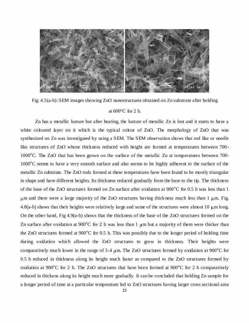
24.51 at. % Zn). Fig. 4.5(a-b) shows that at 600oC the surface of Zn is completely filled with
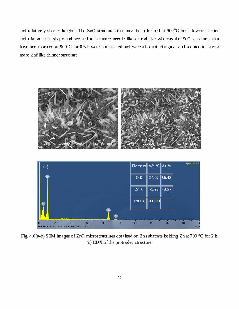
nanostructures of ZnO. There is a wide range of nanostructures of ZnO on the Zn surface. Fig. 4.6(a-b)
shows that the oxidation of Zinc at 700oC does not show any nanostructure of ZnO anymore. There is a
gradual increase in the size of the ZnO structures with further increase in temperature. Fig 4.6(c) shows
the EDX analysis of the ZnO microstructure formed on the Zn surface by heat treating at 700oC for 2 h
shows that the at. % of Zn (43.57 %) and O (56.43 %) are almost identical suggesting that highly
stoichiometric ZnO is formed at this temperature.
19
Fig. 4.1 (a): SEM showing the surface of the as-received pure metallic Zn. (b) EDX analysis of
as-received pure metallic Zn.
Fig. 4.2: SEM showing the surface of the Zn after oxidation at 300oC for 2 h.
Element Weight% Atomic%
Zn K 100.00 100.00
Totals 100.00
(a)
(b)
20
Fig. 4.3(a-b): SEM images showing ZnO nanostructures formed at 400°C on Zn substrate after holding
for a period of 2 h.
Fig. 4.4(a-b): SEM images showing ZnO nanostructures obtained on Zn substrate after holding at 500°C
for 2 h. (c) EDX of the obtained sample
Element Wt. % At. %
O K 13.31 21.59
Zn L 61.74 24.51
(a) (b)
(a) (b)
(c)
21
Fig. 4.5(a-b): SEM images showing ZnO nanostructures obtained on Zn substrate after holding
at 600°C for 2 h.
Zn has a metallic lusture but after heating, the lusture of metallic Zn is lost and it starts to have a
white coloured layer on it which is the typical colour of ZnO. The morphology of ZnO that was
synthesized on Zn was investigated by using a SEM. The SEM observation shows that rod like or needle
like structures of ZnO whose thickness reduced with height are formed at temperatures between 700-
1000oC. The ZnO that has been grown on the surface of the metallic Zn at temperatures between 700-
1000oC seems to have a very smooth surface and also seems to be highly adherent to the surface of the
metallic Zn substrate. The ZnO rods formed at these temperatures have been found to be mostly triangular
in shape and have different heights. Its thickness reduced gradually from the base to the tip. The thickness
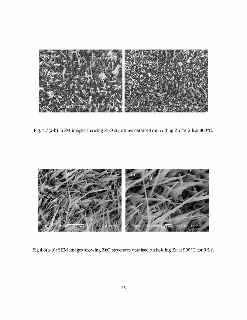
of the base of the ZnO structures formed on Zn surface after oxidation at 900oC for 0.5 h was less than 1
m and there were a large majority of the ZnO structures having thick ness much less than 1 m. Fig.
4.8(a-b) shows that their heights were relatively large and some of the structures were almost 10 m long.
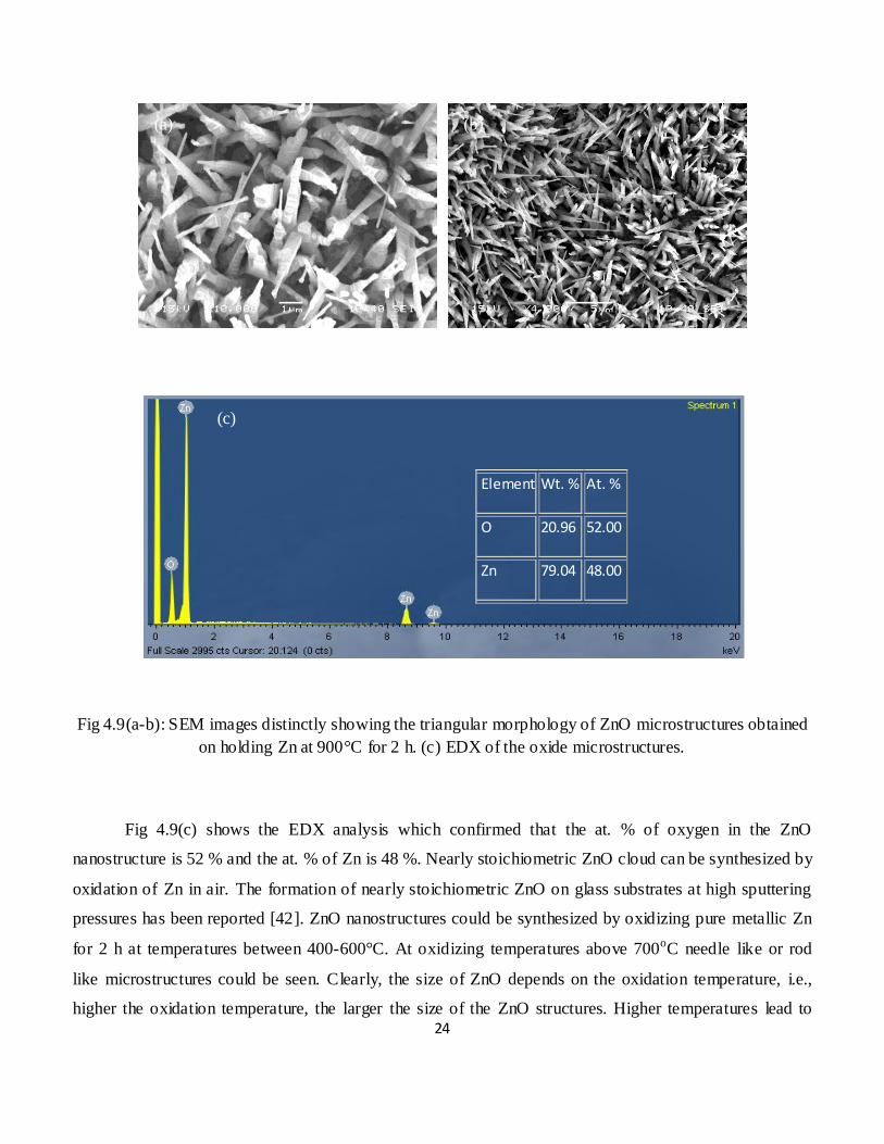
On the other hand, Fig 4.9(a-b) shows that the thickness of the base of the ZnO structures formed on the
Zn surface after oxidation at 900oC for 2 h was less than 1 m but a majority of them were thicker than
the ZnO structures formed at 900oC for 0.5 h. This was possibly due to the longer period of holding time
during oxidation which allowed the ZnO structures to grow in thickness. Their heights were
comparatively much lower in the range of 3-4 m. The ZnO structures formed by oxidation at 900oC for
0.5 h reduced in thickness along its height much faster as compared to the ZnO structures formed by
oxidation at 900oC for 2 h. The ZnO structures that have been formed at 900oC for 2 h comparatively
reduced in thickens along its height much more gradually. It can be concluded that holding Zn sample for
a longer period of time at a particular temperature led to ZnO structures having larger cross sectional area
(a) (b)
22
and relatively shorter heights. The ZnO structures that have been formed at 900oC for 2 h were faceted
and triangular in shape and seemed to be more needle like or rod like whereas the ZnO structures that
have been formed at 900oC for 0.5 h were not faceted and were also not triangular and seemed to have a
more leaf like thinner structure.
Fig. 4.6(a-b) SEM images of ZnO microstructures obtained on Zn substrate holding Zn at 700 °C for 2 h.
(c) EDX of the protruded structure.
Element Wt. % At. %
O K 24.07 56.43
Zn K 75.93 43.57
Totals 100.00
(a) (b)
(c)
23
Fig. 4.7(a-b): SEM images showing ZnO structures obtained on holding Zn for 2 h at 800°C.
Fig 4.8(a-b): SEM images showing ZnO structures obtained on holding Zn at 900°C for 0.5 h.
(a) (b)
(a) (b)
24
Fig 4.9(a-b): SEM images distinctly showing the triangular morphology of ZnO microstructures obtained
on holding Zn at 900°C for 2 h. (c) EDX of the oxide microstructures.
Fig 4.9(c) shows the EDX analysis which confirmed that the at. % of oxygen in the ZnO
nanostructure is 52 % and the at. % of Zn is 48 %. Nearly stoichiometric ZnO cloud can be synthesized by
oxidation of Zn in air. The formation of nearly stoichiometric ZnO on glass substrates at high sputtering
pressures has been reported [42]. ZnO nanostructures could be synthesized by oxidizing pure metallic Zn
for 2 h at temperatures between 400-600°C. At oxidizing temperatures above 700oC needle like or rod
like microstructures could be seen. Clearly, the size of ZnO depends on the oxidation temperature, i.e.,
higher the oxidation temperature, the larger the size of the ZnO structures. Higher temperatures lead to
Element Wt. % At. %
O 20.96 52.00
Zn 79.04 48.00
(a) (b)
(c)
25
more vigorous oxidation and results in mostly columnar needle or rod like structures which are faceted
whereas oxidation at lower temperatures results in nanostructured ZnO. At oxidation temperatures
ranging from 400-600oC nanostructured ZnO having different morphology was formed on the Zn
substrate.
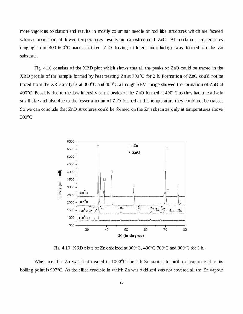
Fig. 4.10 consists of the XRD plot which shows that all the peaks of ZnO could be traced in the
XRD profile of the sample formed by heat treating Zn at 700oC for 2 h. Formation of ZnO could not be
traced from the XRD analysis at 300oC and 400oC although SEM image showed the formation of ZnO at
400oC. Possibly due to the low intensity of the peaks of the ZnO formed at 400oC as they had a relatively
small size and also due to the lesser amount of ZnO formed at this temperature they could not be traced.
So we can conclude that ZnO structures could be formed on the Zn substrates only at temperatures above
300oC.
Fig. 4.10: XRD plots of Zn oxidized at 300oC, 400oC 700oC and 800oC for 2 h.
When metallic Zn was heat treated to 1000oC for 2 h Zn started to boil and vapourized as its
boiling point is 907°C. As the silica crucible in which Zn was oxidized was not covered all the Zn vapour
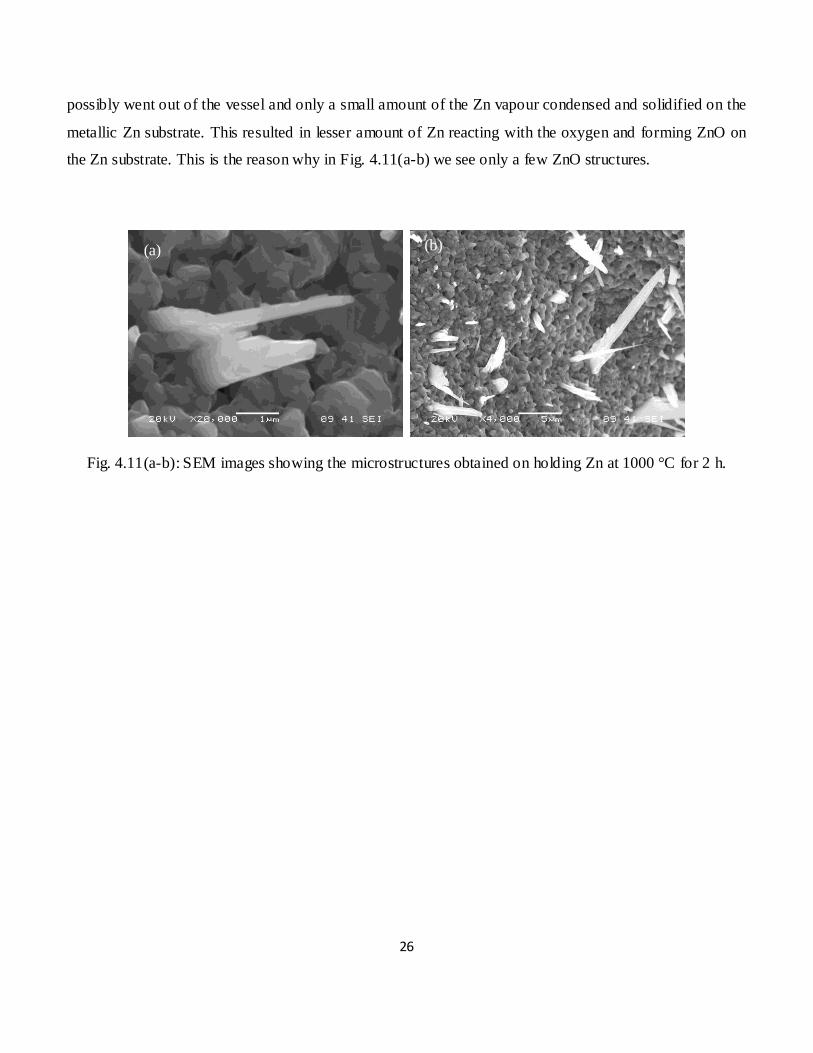
26
possibly went out of the vessel and only a small amount of the Zn vapour condensed and solidified on the
metallic Zn substrate. This resulted in lesser amount of Zn reacting with the oxygen and forming ZnO on
the Zn substrate. This is the reason why in Fig. 4.11(a-b) we see only a few ZnO structures.
Fig. 4.11(a-b): SEM images showing the microstructures obtained on holding Zn at 1000 °C for 2 h.
(a) (b)
27
5.0 Conclusion
In summary, this simple technique of oxidation of metallic Zn in air has been demonstrated as a
very economical and effective technique for the synthesis of ZnO nanostructures on metallic Zn. The ZnO
nanostructures were successfully synthesized by oxidizing pure metallic Zn in the temperature range 400-
600oC. The structure and size of ZnO nanostructures strongly depends on the oxidizing temperatures. This
is an economical route for the synthesis of ZnO on a pure metallic Zn substrate. It is found that the size of
ZnO structures increases with increasing temperature of oxidation.
The scanning electron microscopy observation shows that needle like or rod like structures of ZnO
could be formed at temperatures above 700oC. Above the oxidizing temperature of 700oC the needle like
or rod like structures of ZnO were very uniform in shape and size. The Zn surface was covered densely
with the ZnO structures at oxidation temperatures above 700oC. On the other hand at oxidizing
temperatures between 400-600oC the nanostructured ZnO were nonuniform in size and structure and were
less dense and more scattered on the metallic Zn surface.
28
6.0 References
[1] Zhong Lin Wang, Zinc oxide nanostructures: growth, properties and applications, Journal of Physics:
Condensed Matter. Vol. 16 (2004), R829- R858 [2] http://www.chemistry.ohio-state.edu/~woodward/ch754/struct/ZnO.htm
[3] Zhiyong Fan and Jia G. Lu, Zinc Oxide Nanostructures: Synthesis and Properties, Journal of
Nanoscience and Nanotechnology. Vol. 5 (2005) (10), pp. 1561-1573.
[4] S Baruah and J Dutta, Hydrothermal growth of ZnO nanostructures, Sci. Technol. Adv. Mater. Vol. 10 (2009) (1).
[5] Hernandezbattez, A; Gonzalez, R; Viesca, J; Fernandez, J; Diazfernandez, J; MacHado, A; Chou, R;
Riba, J; CuO, ZrO2 and ZnO nanoparticles as antiwear additive in oil lubricants. (2008), pp. 265.
[6] Porter, F, Zinc Handbook: Properties, Processing, and Use in Design, CRC Press. (1991).
[7] Dapeng Wu, Zhengyu Bai, Kai Jiang,Temperature induced hierarchical growth of ZnO microcrystal,
Materials Letters. Vol. 63 (2009), pp. 1057-1060.
[8] Chen, Z., Z. Shan, S. Li, C.B. Liang, and S.X. Mao. 2004. A novel and simple growth route towards ultra- fine ZnO nanowires. J. Cryst. Growth. Vol. 265, pp. 482–486.
[9] Sekar, A., S. H. Kim, A. Umar, and Y. B. Hahn. 2005. Catalyst- free synthesis of ZnO nanowires on Si
by oxidation of Zn powders. J. Cryst. Growth. Vol. 277, pp. 471–478.
[10] Zhang, J., Y. Yang, B. Xu, F. Jiang, and J. Li. 2005. Shape-controlled synthesis of ZnO nano and
micro-structures. J. Cryst. Growth. Vol. 280, pp. 509–515.
[11] T. K. Subramanyam, B. Srinivasulu Naidu, S. Uthanna, Physical Properties of Zinc Oxide Films
Prepared by DC Reactive Magnetron Sputtering at Different Sputtering Pressures, Cryst. Res. Technol.
Vol. 35 (2000) (10), pp. 1194-1202.
[12] Wang, Zhong Lin, Zinc oxide nanostructures: Growth, properties and applications, J. Phys.:
Condens. Matter. Vol. 16 (2004), pp. R829–R858.
[13] Yang Liu, Jian-er Zhou, Andre Larbot , Michel Persin, Preparation and characterization of
nano Zinc oxide, Journal of Materials Processing Technology. Vol. 189 (2007), pp. 379–383.
[14] T. K. Subramanyam, B. Srinivasulu Naidu, S. Uthanna, Physical Properties of Zinc Oxide Films
Prepared by dc Reactive Magnetron Sputtering at Different Sputtering Pressures, Cryst. Res. Technol.
Vol. 35 (2000), pp. 1193–1202.
29
[15] T.A. Polley, W.B. Carter, D.B. Poker, Deposition of Zinc oxide thin films by combustion CVD, Thin
Solid Films. Vol. 357 (1999), pp. 132-136.
[16] Ü. Özgür, Ya. I. Alivov, C. Liu, A. Teke, M. A. Reshchikov, S. Doğan, V. Avrutin,
S.-J. Cho, and H. Morkoç, A comprehensive review of ZnO materials and devices, Journal of applied
physics. Vol. 98 (2005), pp. 041301.
[17] B. Wang, E. Shi, W. Zhong, C. Xia, W. Li, Z. Yin, Growth habits and mechanism of ZnO, Micro-
Cryst. Hydrotherm. Cond. Vol. 25 (1997) (2), pp. 223.
[18] S.H. Jo, J.Y. Lao, Z.F. Ren, et al., Field-emission studies on thin films of
Zinc oxide nanowires, Appl. Phys. Lett. Vol. 83 (2003) (23), pp. 4821.
[19] P.X. Gao, Z.L.Wang, Nanopropeller arrays of zinc oxide, Appl. Phys. Lett. Vol. 84(2004) (15), pp.
2883.
[20] Zhiyong Fan and Jia G. Lu, Zinc Oxide Nanostructures: Synthesis and Properties, Journal of
Nanoscience and Nanotechnology. Vol. 5(2005) (10), pp. 1561-1573.
[21] B. M. Ataev, I. K. Kamilov, A. M. Bagamadova, V. V. Mamedov,S. Sh. Makhmudov, A. K. Omaev,
and Sh. O. Shakhshaev, Controlled Growth of Quasibicrystal Zinc Oxide Structures. Technical Physics
Letters. Vol. 26 (2000) (9), pp. 837–838.
[22] INCAPentaFET-x3, (2008), Retrieved April 22 2010 from
http://www.oxford-instruments.com/products/microanalysis/eds/detectors/sili-
detector/Pages/incapentafet-x3.aspx
[23] Raghu Viswanathan, Ram B. Gupta, Formation of zinc oxide nanoparticles in supercritical water, J.
of Supercritical Fluids. Vol. 27 (2003), pp. 187-193.
[24] Zhiyong Xu, Jiann-Yang Hwang, Bowen Li, Xiaodi Huang, and Howard Wang, The Characterization
of Various ZnO Nanostructures Using Field-Emission SEM, Research summary
(www.tms.org/jom.html).
[25] K Sreenivas, Sanjeev Kumar, Jaya Choudhary and Vinay gupta, Growth of zinc oxide
nanostructures.Journal of Phy. Vol. 65 (2005) (5), pp. 809-814.
30
[26] A. N. Red‟kin, Z. I. Makovei, A. N. Gruzintsev, E. E. Yakimov, O. V. Kononenko, and A. A. Firsov,
Elemental Vapor-Phase Synthesis of Nanostructured Zinc Oxide. ISSN 0020-1685, Inorganic
Materials.Vol. 45 (2009) (11), pp. 1246–1251.
[27] S Roy and S Basu, Improved zinc oxide film for gas sensor applications. Bull. Mater. Sci. Vol. 25
(2002) (6), pp. 513–515.
[28] Instrument Database:JEOL - JSM-6480LV, (2007), Retrieved April 22, 2010 from
http://www.speciation.net/Appl/Techniques/technique.html?id=47
[29] Zhong Lin Wang, Nanostructures of ZnO, Materials Today. Vol. 7 (2004) (6), pp. 26-33.
[30] S. Music´, S. Popovic´, M. Maljkovic´, D. Dragcˇevic, Influence of synthesis procedure on the
formation and properties of Zinc oxide. Journal of Alloys and Compounds. Vol. 347 (2002), pp. 324–332
[31] Basics of X Ray Diffraction, Scintag Inc.,1999, Chapter 7, pp. 7.13-7.14.
[32] T. K. Subramanyam, B. Srinivasulu Naidu, S. Uthanna, Structure and Optical Properties of DC
Reactive Magnetron Sputtered Zinc Oxide Films. Cryst. Res. Technol. Vol. 34 (1999), pp. 981–988
[33] Yousheng Zhang, Lisheng Wang, Xiaohua Liu, Yunjie Yan, Changqiang Chen, and Jing Zhu,
Synthesis of Nano/Micro Zinc oxide Rods and Arrays by Thermal Evaporation Approach on Cylindrical
Shape Substrate. J. Phys. Chem. B. Vol. 109 (2005) (27), pp. 13091-13093.
[34] C.K.Yap,W.C.Tan, S.S.Alias, A.A.Mohamad, Synthesis of zinc oxide by zinc–air system. J. Alloys
Compd. Journal of Alloys and Compounds. Vol. 484 (2009) (1-2), pp. 934-938.
[35] Li ChenSha, Li YuNing, Wu YiLiang, Beng S. Ong & Rafik O. Loutfy, Synthesis of Zinc oxide
nanocrystals by thermal decomposition of Zn-oleate in organic medium,
Sci China Ser E-Tech Sci. Vol. 51 (2008) (12), pp. 2075-2079.
[36] Dapeng Wu, Zhengyu Bai, Kai Jiang, Temperature induced hierarchical growth of ZnO microcrystal,
Materials Letters. Vol. 63 (2009), pp. 1057–1060.
[37] C.W. Yao, H.P. Wu, M.Y. Ge, L. Yang, Y.W. Zeng, Y.W. Wang , J.Z. Jiang, Triangle-shape ZnO
prepared by thermal decomposition, Materials Letters. Vol. 61 (2007), pp. 3416–3420.
[38] Orathai Yawong, Supab Choopun, Pongsri Mangkorntong and Nikorn Mangkorntong, Zinc Oxide Nanostructure by Oxidization of Zinc Thin Films. Chiang Mai University Journal Special Issue On
Nanotechnology. Vol. 4 (2005) (1).

31
[39] Industrial applications of ZnO, Retrieved April 22, 2010 from
http://navbharat.co.in/clients.htm
[40] Energy Dispersive X-ray Spectroscopy (EDS), John Goodge, University of Minnesota-Duluth,
Retrieved April 22, 2010 from http://serc.carleton.edu/research_education/geochemsheets/eds.html
[41] Scanning Electron Microscopy (SEM), Susan Swapp, University of Wyoming, Retrieved April 22
2010 from
http://serc.carleton.edu/research_education/geochemsheets/techniques/SEM.html
[42] Single Crystal X-ray Diffraction, Christine M. Clark, Eastern Michigan University,Barbara L.
Dutrow, Louisiana State University, Retrieved April 22 2010 from
http://serc.carleton.edu/research_education/geochemsheets/techniques/SXD.html
[43] Regional Sophisticated Instrumentation Centre PU, Chd, Retrieved on May 4,2010 from
http://rsic.puchd.ac.in/em.html
[44] What is SEM? Iowa State Varsity, MME dept., Retrieved on May 4, 2010 from
http://mse.iastate.edu/microscopy/whatsem.html
[45] Sato, H., Minami, T., Takata, S., Mouri, T., Ogawa, N. Thin Solid Films, Vol. 220 (1992), pp. 327
and Vol. 246 (1994), pp. 86.
[46] Zinc oxide applications, Retrieved on May 4, 2010 from
http://www.stallonezincoxide.com/application.htm
[47] Zinc oxide (ZnO) – Properties and Applications, Retrieved on May 4, 2010 from
http://www.azom.com/details.asp?ArticleID=2357
[48] Zinc oxide applications, Retrieved on May 4, 2010 from
http://www.ucalanka.com/zinc-oxide-applications.html
[49] Zinc oxide application, Retrieved on May 4, 2010 from
http://www.numinor.com/application.asp
[50] Zinc oxide applications, Retrieved on May 4, 2010 from http://wapedia.mobi/en/Zinc_oxide?t=6.


![Bending piezoelectric nanowires: application to force ...€¦ · [6] D. Lincot, “Solution growth of functional zinc oxide films and nanostructures,” MRS Bull., vol. 35, no. October,](https://img.pdfslide.us/doc/110x75/5ea804eb2022bf2e5242886b/bending-piezoelectric-nanowires-application-to-force-6-d-lincot-aoesolution.jpg)