Embed Size (px)
Citation preview
1
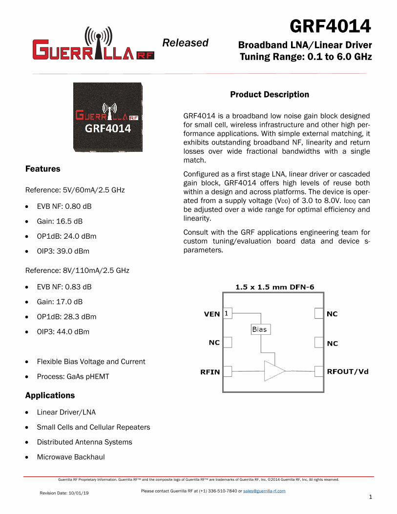
GRF4014
Guerrilla RF Proprietary Information. Guerrilla RFTM and the composite logo of Guerrilla RFTM are trademarks of Guerrilla RF, Inc. ©2014 Guerrilla RF, Inc. All rights reserved.
Revision Date: 10/01/19 Please contact Guerrilla RF at (+1) 336-510-7840 or [email protected]
Released Broadband LNA/Linear Driver
Tuning Range: 0.1 to 6.0 GHz
GRF4014 is a broadband low noise gain block designed
for small cell, wireless infrastructure and other high per-
formance applications. With simple external matching, it
exhibits outstanding broadband NF, linearity and return
losses over wide fractional bandwidths with a single
match.
Configured as a first stage LNA, linear driver or cascaded
gain block, GRF4014 offers high levels of reuse both
within a design and across platforms. The device is oper-
ated from a supply voltage (VDD) of 3.0 to 8.0V. IDDQ can
be adjusted over a wide range for optimal efficiency and
linearity.
Consult with the GRF applications engineering team for
custom tuning/evaluation board data and device s-
parameters.
Product Description
Features
Reference: 5V/60mA/2.5 GHz
• EVB NF: 0.80 dB
• Gain: 16.5 dB
• OP1dB: 24.0 dBm
• OIP3: 39.0 dBm
Reference: 8V/110mA/2.5 GHz
• EVB NF: 0.83 dB
• Gain: 17.0 dB
• OP1dB: 28.3 dBm
• OIP3: 44.0 dBm
• Flexible Bias Voltage and Current
• Process: GaAs pHEMT
Applications
• Linear Driver/LNA
• Small Cells and Cellular Repeaters
• Distributed Antenna Systems
• Microwave Backhaul
2
GRF4014
Guerrilla RF Proprietary Information. Guerrilla RFTM and the composite logo of Guerrilla RFTM are trademarks of Guerrilla RF, Inc. ©2014 Guerrilla RF, Inc. All rights reserved.
Revision Date: 10/01/19 Please contact Guerrilla RF at (+1) 336-510-7840 or [email protected]
Released Broadband LNA/Linear Driver
Tuning Range: 0.1 to 6.0 GHz
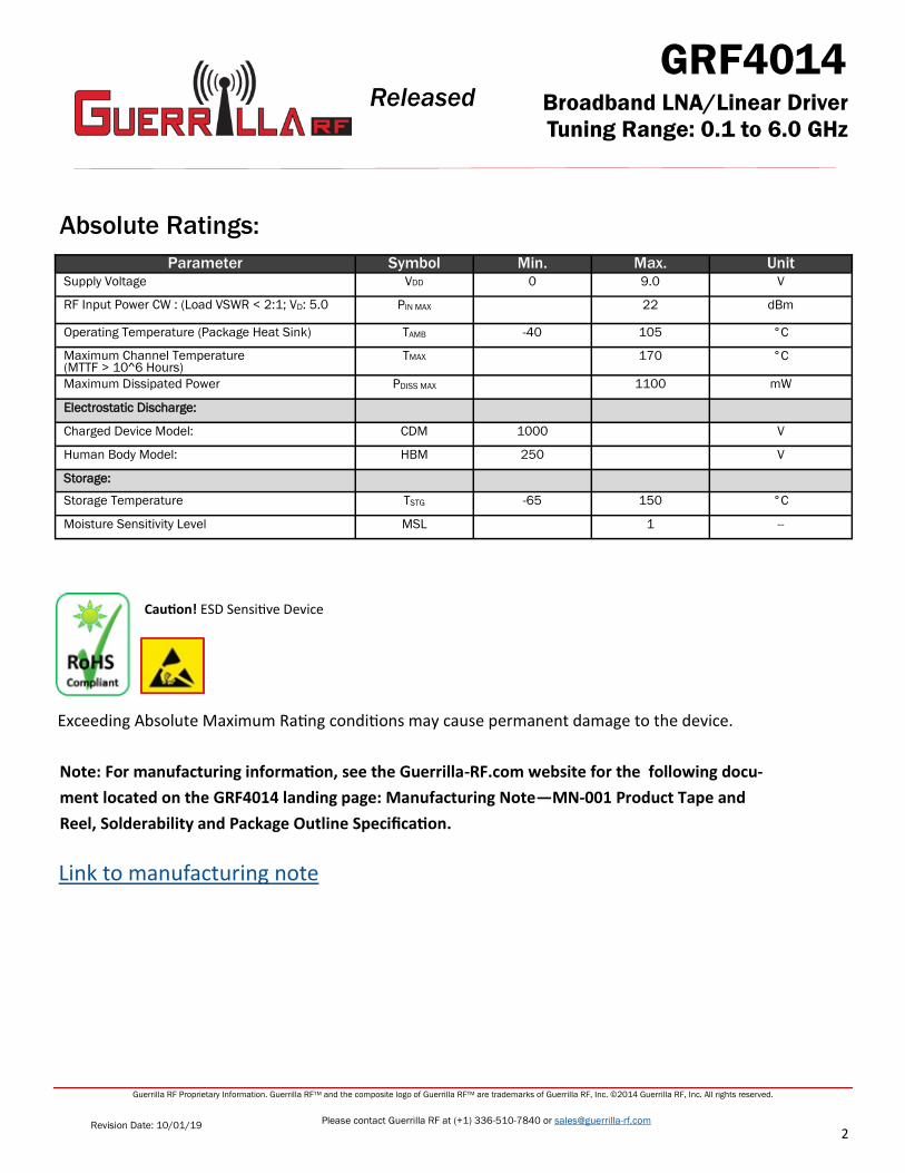
Parameter Symbol Min. Max. Unit Supply Voltage VDD 0 9.0 V
RF Input Power CW : (Load VSWR < 2:1; VD: 5.0 PIN MAX 22 dBm
Operating Temperature (Package Heat Sink) TAMB -40 105 °C
Maximum Channel Temperature (MTTF > 10^6 Hours)
TMAX 170 °C
Maximum Dissipated Power PDISS MAX 1100 mW
Electrostatic Discharge:
Charged Device Model: CDM 1000 V
Human Body Model: HBM 250 V
Storage:
Storage Temperature TSTG -65 150 °C
Moisture Sensitivity Level MSL 1 --
Absolute Ratings:
Caution! ESD Sensitive Device
Exceeding Absolute Maximum Rating conditions may cause permanent damage to the device.
Note: For manufacturing information, see the Guerrilla-RF.com website for the following docu-
ment located on the GRF4014 landing page: Manufacturing Note—MN-001 Product Tape and
Reel, Solderability and Package Outline Specification.
Link to manufacturing note
3
GRF4014
Guerrilla RF Proprietary Information. Guerrilla RFTM and the composite logo of Guerrilla RFTM are trademarks of Guerrilla RF, Inc. ©2014 Guerrilla RF, Inc. All rights reserved.
Revision Date: 10/01/19 Please contact Guerrilla RF at (+1) 336-510-7840 or [email protected]
Released Broadband LNA/Linear Driver
Tuning Range: 0.1 to 6.0 GHz
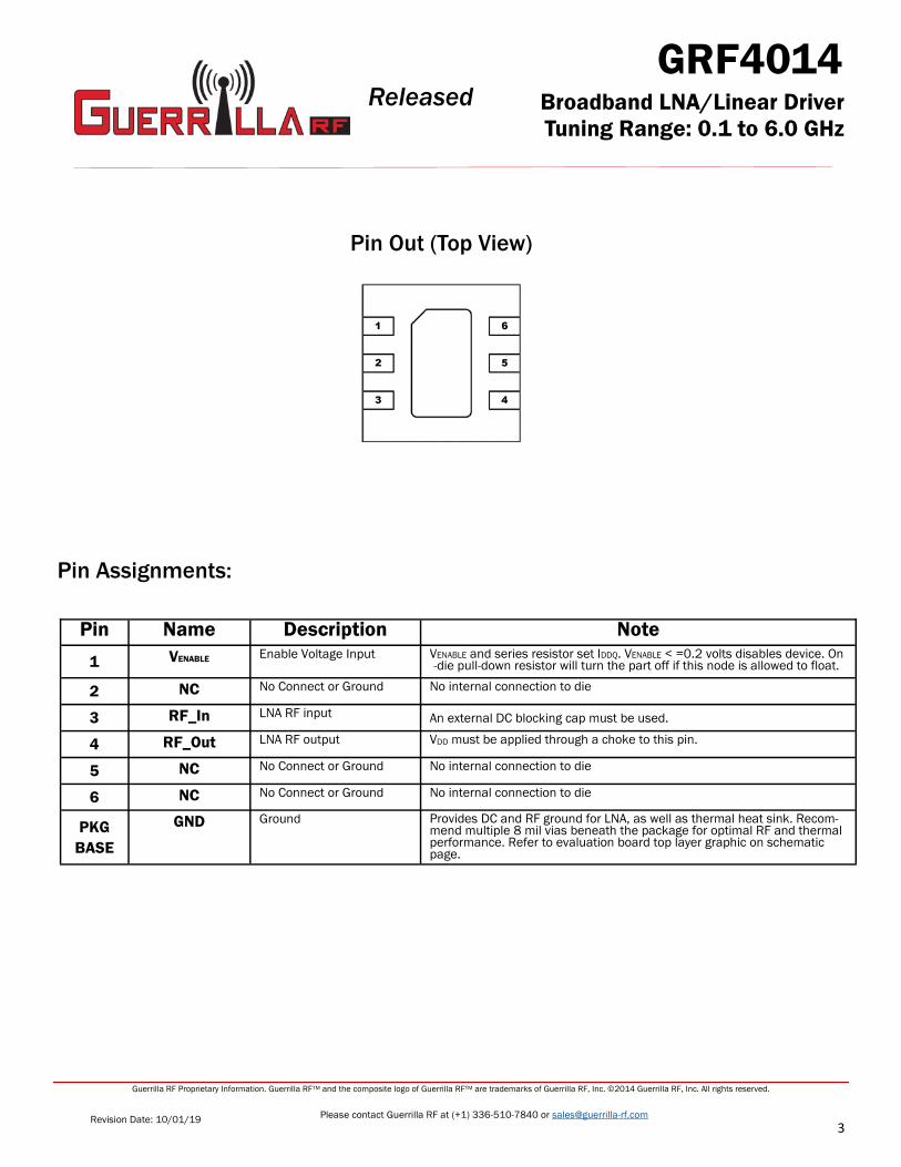
Pin Out (Top View)
Pin Assignments:
Pin Name Description Note
1 VENABLE Enable Voltage Input VENABLE and series resistor set IDDQ. VENABLE < =0.2 volts disables device. On-die pull-down resistor will turn the part off if this node is allowed to float.
2 NC No Connect or Ground No internal connection to die
3 RF_In LNA RF input An external DC blocking cap must be used.
4 RF_Out LNA RF output VDD must be applied through a choke to this pin.
5 NC No Connect or Ground No internal connection to die
6 NC No Connect or Ground No internal connection to die
PKG
BASE
GND Ground Provides DC and RF ground for LNA, as well as thermal heat sink. Recom-mend multiple 8 mil vias beneath the package for optimal RF and thermal performance. Refer to evaluation board top layer graphic on schematic page.
4
GRF4014
Guerrilla RF Proprietary Information. Guerrilla RFTM and the composite logo of Guerrilla RFTM are trademarks of Guerrilla RF, Inc. ©2014 Guerrilla RF, Inc. All rights reserved.
Revision Date: 10/01/19 Please contact Guerrilla RF at (+1) 336-510-7840 or [email protected]
Released Broadband LNA/Linear Driver
Tuning Range: 0.1 to 6.0 GHz
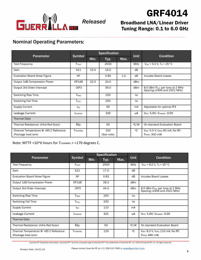
Nominal Operating Parameters:
Parameter Symbol Specification
Unit Condition Min. Typ. Max.
Test Frequency FTEST 2500 MHz VDD = 5.0 V, TA = 25°C
Gain S21 15.5 16.5 dB
Evaluation Board Noise Figure NF 0.80 1.0 dB Incudes Board Losses
Output 1dB Compression Power OP1dB 22.5 24.0 dBm
Output 3rd Order Intercept OIP3 39.0 dBm 8.0 dBm POUT per tone at 2 MHz Spacing (2499 and 2501 MHz)
Switching Rise Time TRISE 200 ns
Switching Fall Time TFALL 200 ns
Supply Current IDD 60 mA Adjustable for optimal IP3
Leakage Current ILEAKAGE 250 uA VDD: 5.0V; VENABLE: 0.0V
Thermal Data
Thermal Resistance: (Infra-Red Scan) jc 50 ᵒC/W On standard Evaluation Board
Channel Temperature @ +85 C Reference (Package heat sink)
TCHANNEL 100
(See note)
ᵒC VDD: 5.0 V; IDDQ: 60 mA; No RF; PDISS: 300 mW
Parameter Symbol Specification
Unit Condition Min. Typ. Max.
Test Frequency FTEST 2500 MHz VDD = 8.0 V, TA = 25°C
Gain S21 17.0 dB
Evaluation Board Noise Figure NF 0.83 dB Incudes Board Losses
Output 1dB Compression Power OP1dB 28.3 dBm
Output 3rd Order Intercept OIP3 44.0 dBm 8.0 dBm POUT per tone at 2 MHz Spacing (2499 and 2501 MHz)
Switching Rise Time TRISE 200 ns
Switching Fall Time TFALL 200 ns
Supply Current IDD 110 mA
Leakage Current ILEAKAGE 325 uA VDD: 5.0V; VENABLE: 0.0V
Thermal Data
Thermal Resistance: (Infra-Red Scan) jc 50 ᵒC/W On standard Evaluation Board
Channel Temperature @ +85 C Reference (Package heat sink)
TCHANNEL 129 ᵒC VDD: 8.0 V; IDDQ: 110 mA; No RF; PDISS: 880 mW
Note: MTTF >10^6 hours for TCHANNEL < =170 degrees C.
5
GRF4014
Guerrilla RF Proprietary Information. Guerrilla RFTM and the composite logo of Guerrilla RFTM are trademarks of Guerrilla RF, Inc. ©2014 Guerrilla RF, Inc. All rights reserved.
Revision Date: 10/01/19 Please contact Guerrilla RF at (+1) 336-510-7840 or [email protected]
Released Broadband LNA/Linear Driver
Tuning Range: 0.1 to 6.0 GHz
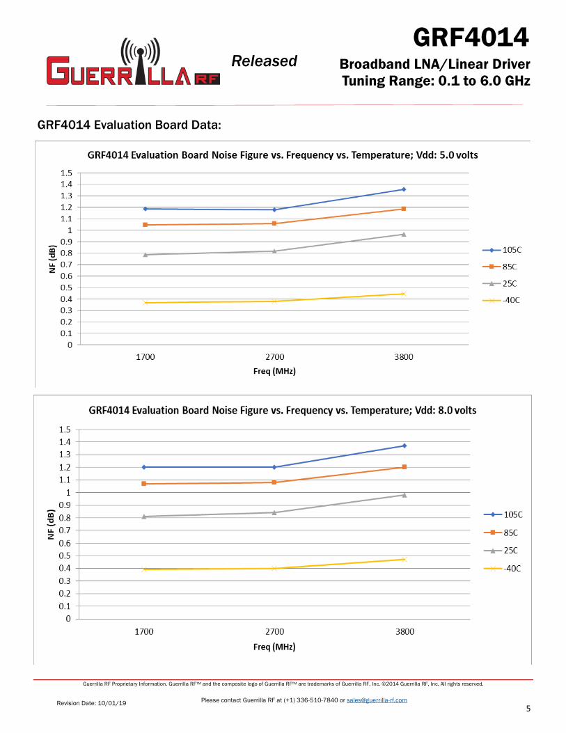
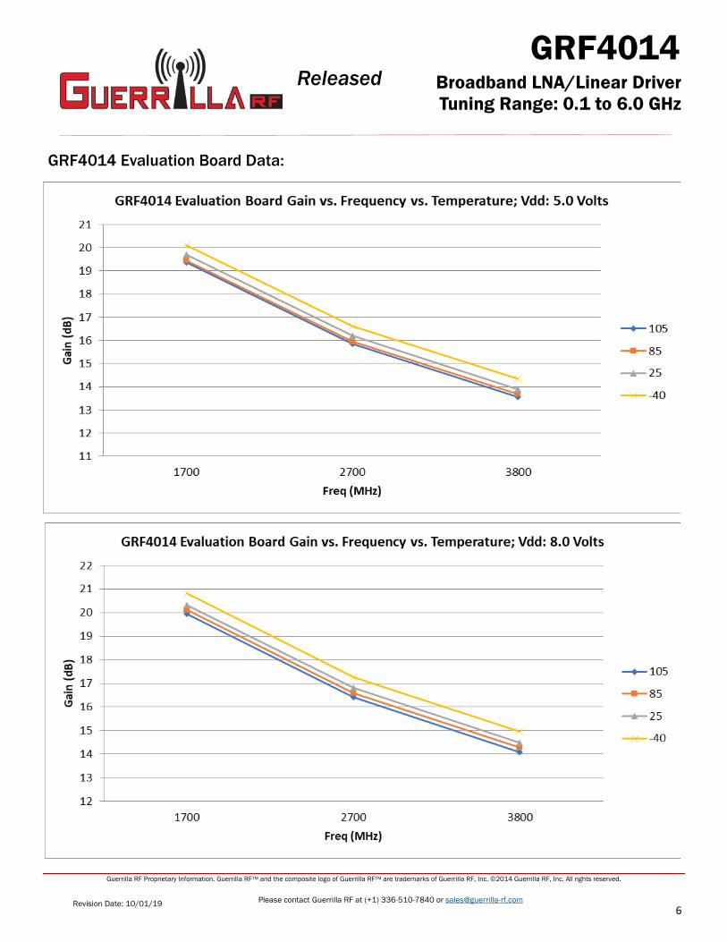
GRF4014 Evaluation Board Data:
6
GRF4014
Guerrilla RF Proprietary Information. Guerrilla RFTM and the composite logo of Guerrilla RFTM are trademarks of Guerrilla RF, Inc. ©2014 Guerrilla RF, Inc. All rights reserved.
Revision Date: 10/01/19 Please contact Guerrilla RF at (+1) 336-510-7840 or [email protected]
Released Broadband LNA/Linear Driver
Tuning Range: 0.1 to 6.0 GHz
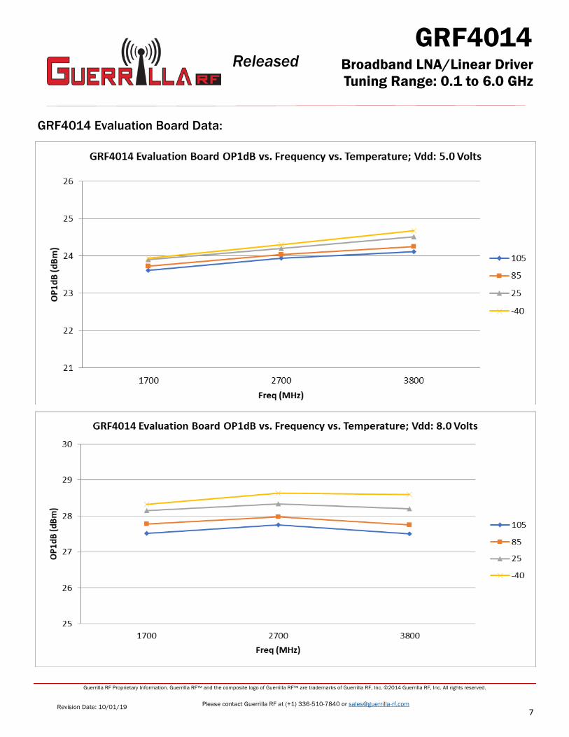
GRF4014 Evaluation Board Data:
7
GRF4014
Guerrilla RF Proprietary Information. Guerrilla RFTM and the composite logo of Guerrilla RFTM are trademarks of Guerrilla RF, Inc. ©2014 Guerrilla RF, Inc. All rights reserved.
Revision Date: 10/01/19 Please contact Guerrilla RF at (+1) 336-510-7840 or [email protected]
Released Broadband LNA/Linear Driver
Tuning Range: 0.1 to 6.0 GHz
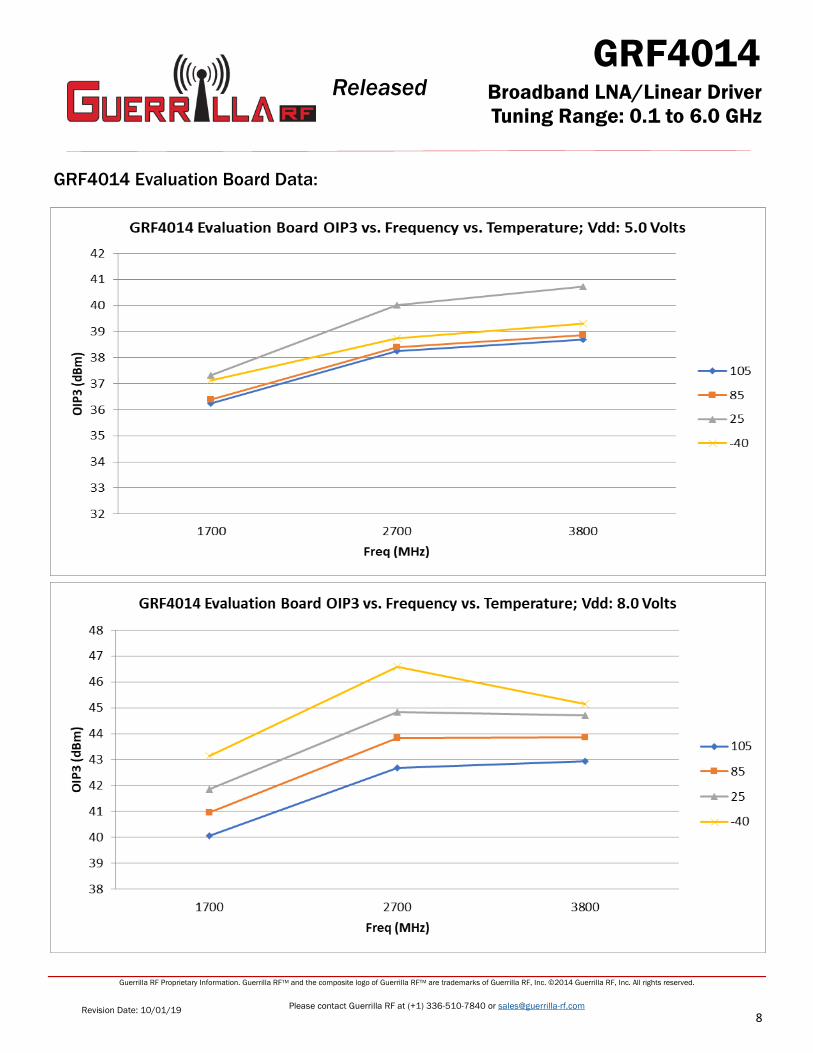
GRF4014 Evaluation Board Data:
8
GRF4014
Guerrilla RF Proprietary Information. Guerrilla RFTM and the composite logo of Guerrilla RFTM are trademarks of Guerrilla RF, Inc. ©2014 Guerrilla RF, Inc. All rights reserved.
Revision Date: 10/01/19 Please contact Guerrilla RF at (+1) 336-510-7840 or [email protected]
Released Broadband LNA/Linear Driver
Tuning Range: 0.1 to 6.0 GHz
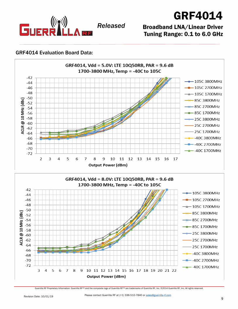
GRF4014 Evaluation Board Data:
9
GRF4014
Guerrilla RF Proprietary Information. Guerrilla RFTM and the composite logo of Guerrilla RFTM are trademarks of Guerrilla RF, Inc. ©2014 Guerrilla RF, Inc. All rights reserved.
Revision Date: 10/01/19 Please contact Guerrilla RF at (+1) 336-510-7840 or [email protected]
Released Broadband LNA/Linear Driver
Tuning Range: 0.1 to 6.0 GHz
GRF4014 Evaluation Board Data:
10
GRF4014
Guerrilla RF Proprietary Information. Guerrilla RFTM and the composite logo of Guerrilla RFTM are trademarks of Guerrilla RF, Inc. ©2014 Guerrilla RF, Inc. All rights reserved.
Revision Date: 10/01/19 Please contact Guerrilla RF at (+1) 336-510-7840 or [email protected]
Released Broadband LNA/Linear Driver
Tuning Range: 0.1 to 6.0 GHz
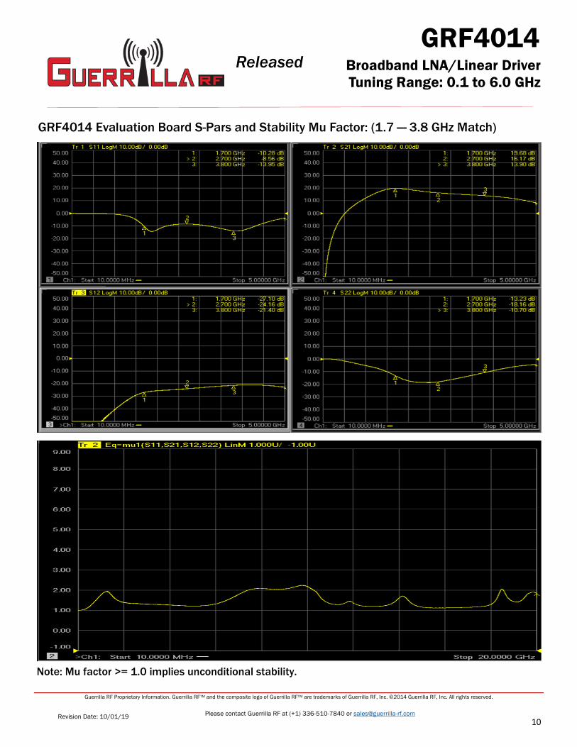
GRF4014 Evaluation Board S-Pars and Stability Mu Factor: (1.7 — 3.8 GHz Match)
Note: Mu factor >= 1.0 implies unconditional stability.
11
GRF4014
Guerrilla RF Proprietary Information. Guerrilla RFTM and the composite logo of Guerrilla RFTM are trademarks of Guerrilla RF, Inc. ©2014 Guerrilla RF, Inc. All rights reserved.
Revision Date: 10/01/19 Please contact Guerrilla RF at (+1) 336-510-7840 or [email protected]
Released Broadband LNA/Linear Driver
Tuning Range: 0.1 to 6.0 GHz
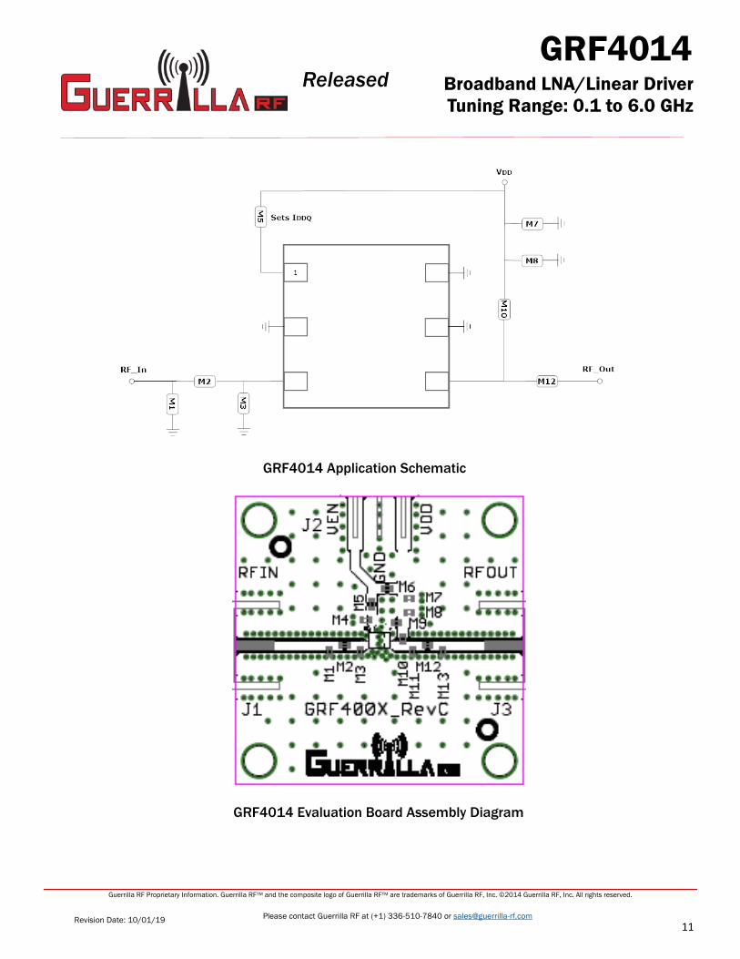
GRF4014 Application Schematic
GRF4014 Evaluation Board Assembly Diagram
12
GRF4014
Guerrilla RF Proprietary Information. Guerrilla RFTM and the composite logo of Guerrilla RFTM are trademarks of Guerrilla RF, Inc. ©2014 Guerrilla RF, Inc. All rights reserved.
Revision Date: 10/01/19 Please contact Guerrilla RF at (+1) 336-510-7840 or [email protected]
Released Broadband LNA/Linear Driver
Tuning Range: 0.1 to 6.0 GHz
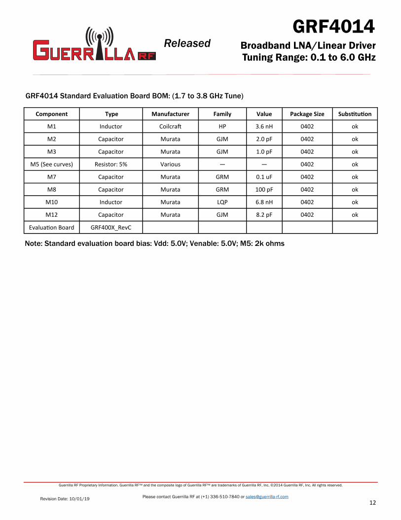
Component Type Manufacturer Family Value Package Size Substitution
M1 Inductor Coilcraft HP 3.6 nH 0402 ok
M2 Capacitor Murata GJM 2.0 pF 0402 ok
M3 Capacitor Murata GJM 1.0 pF 0402 ok
M5 (See curves) Resistor: 5% Various — — 0402 ok
M7 Capacitor Murata GRM 0.1 uF 0402 ok
M8 Capacitor Murata GRM 100 pF 0402 ok
M10 Inductor Murata LQP 6.8 nH 0402 ok
M12 Capacitor Murata GJM 8.2 pF 0402 ok
Evaluation Board GRF400X_RevC
GRF4014 Standard Evaluation Board BOM: (1.7 to 3.8 GHz Tune)
Note: Standard evaluation board bias: Vdd: 5.0V; Venable: 5.0V; M5: 2k ohms
13
GRF4014
Guerrilla RF Proprietary Information. Guerrilla RFTM and the composite logo of Guerrilla RFTM are trademarks of Guerrilla RF, Inc. ©2014 Guerrilla RF, Inc. All rights reserved.
Revision Date: 10/01/19 Please contact Guerrilla RF at (+1) 336-510-7840 or [email protected]
Released Broadband LNA/Linear Driver
Tuning Range: 0.1 to 6.0 GHz
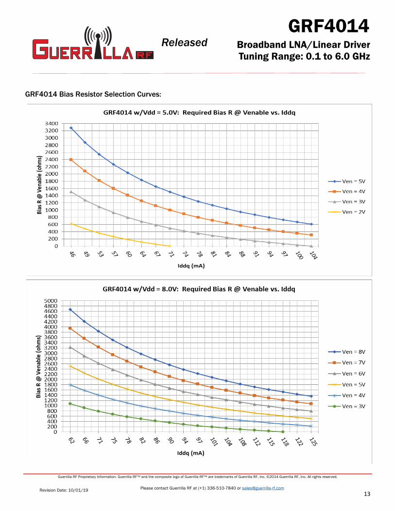
GRF4014 Bias Resistor Selection Curves:
14
GRF4014
Guerrilla RF Proprietary Information. Guerrilla RFTM and the composite logo of Guerrilla RFTM are trademarks of Guerrilla RF, Inc. ©2014 Guerrilla RF, Inc. All rights reserved.
Revision Date: 10/01/19 Please contact Guerrilla RF at (+1) 336-510-7840 or [email protected]
Released Broadband LNA/Linear Driver
Tuning Range: 0.1 to 6.0 GHz
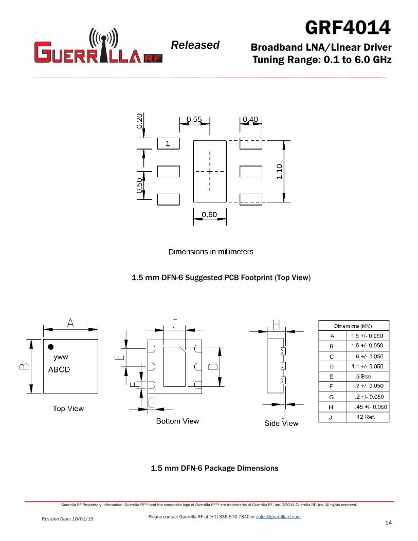
1.5 mm DFN-6 Suggested PCB Footprint (Top View)
1.5 mm DFN-6 Package Dimensions
15
GRF4014
Guerrilla RF Proprietary Information. Guerrilla RFTM and the composite logo of Guerrilla RFTM are trademarks of Guerrilla RF, Inc. ©2014 Guerrilla RF, Inc. All rights reserved.
Revision Date: 10/01/19 Please contact Guerrilla RF at (+1) 336-510-7840 or [email protected]
Released Broadband LNA/Linear Driver
Tuning Range: 0.1 to 6.0 GHz
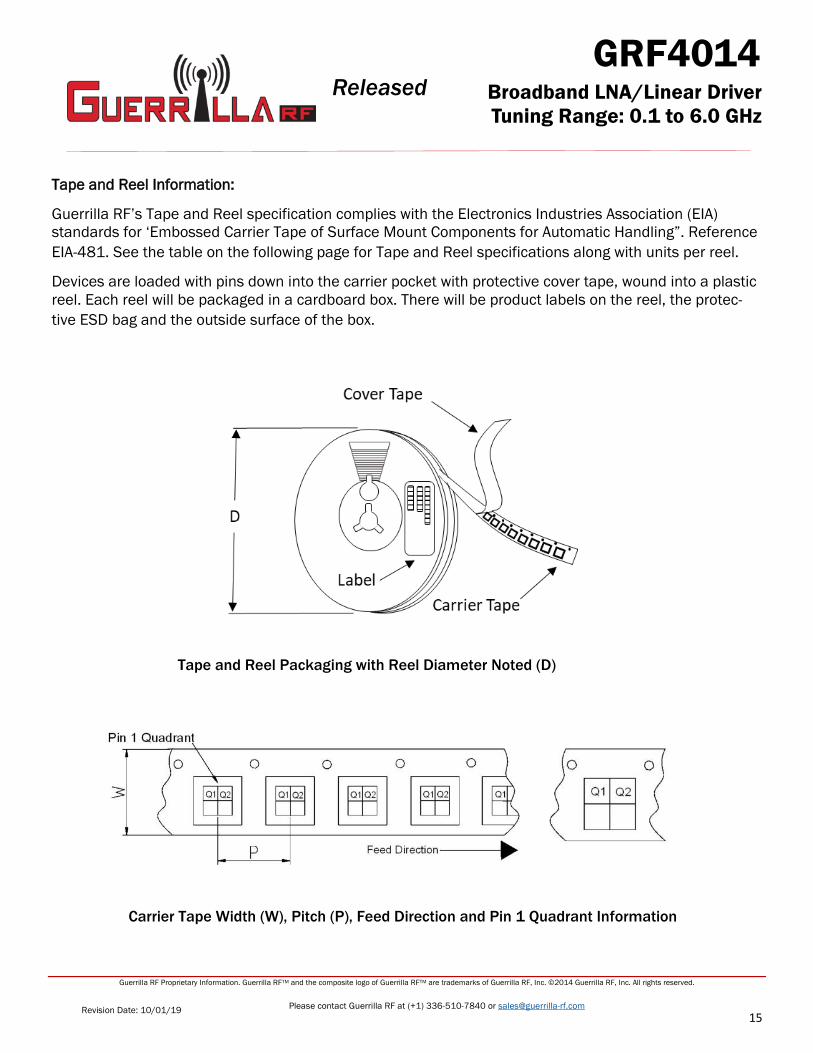
Tape and Reel Information:
Guerrilla RF’s Tape and Reel specification complies with the Electronics Industries Association (EIA)
standards for ‘Embossed Carrier Tape of Surface Mount Components for Automatic Handling”. Reference
EIA-481. See the table on the following page for Tape and Reel specifications along with units per reel.
Devices are loaded with pins down into the carrier pocket with protective cover tape, wound into a plastic
reel. Each reel will be packaged in a cardboard box. There will be product labels on the reel, the protec-
tive ESD bag and the outside surface of the box.
Carrier Tape Width (W), Pitch (P), Feed Direction and Pin 1 Quadrant Information
Tape and Reel Packaging with Reel Diameter Noted (D)
16
GRF4014
Guerrilla RF Proprietary Information. Guerrilla RFTM and the composite logo of Guerrilla RFTM are trademarks of Guerrilla RF, Inc. ©2014 Guerrilla RF, Inc. All rights reserved.
Revision Date: 10/01/19 Please contact Guerrilla RF at (+1) 336-510-7840 or [email protected]
Released Broadband LNA/Linear Driver
Tuning Range: 0.1 to 6.0 GHz
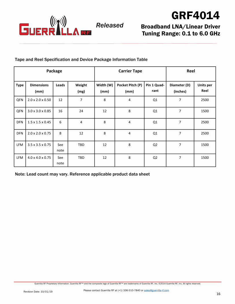
Tape and Reel Specification and Device Package Information Table
Note: Lead count may vary. Reference applicable product data sheet
Package Carrier Tape Reel
Type Dimensions
(mm)
Leads Weight
(mg)
Width (W)
(mm)
Pocket Pitch (P)
(mm)
Pin 1 Quad-
rant
Diameter (D)
(inches)
Units per
Reel
QFN 2.0 x 2.0 x 0.50 12 7 8 4 Q1 7 2500
QFN 3.0 x 3.0 x 0.85 16 24 12 8 Q1 7 1500
DFN 1.5 x 1.5 x 0.45 6 4 8 4 Q1 7 2500
DFN 2.0 x 2.0 x 0.75 8 12 8 4 Q1 7 2500
LFM 3.5 x 3.5 x 0.75 See
note
TBD 12 8 Q2 7 1500
LFM 4.0 x 4.0 x 0.75 See
note
TBD 12 8 Q2 7 1500
17
GRF4014
Guerrilla RF Proprietary Information. Guerrilla RFTM and the composite logo of Guerrilla RFTM are trademarks of Guerrilla RF, Inc. ©2014 Guerrilla RF, Inc. All rights reserved.
Revision Date: 10/01/19 Please contact Guerrilla RF at (+1) 336-510-7840 or [email protected]
Released Broadband LNA/Linear Driver
Tuning Range: 0.1 to 6.0 GHz
Data Sheet Release Status: Notes
Advance S-parameter and NF data based on EM simulations for the fully packaged device
using foundry supplied transistor s-parameters. Linearity estimates based on de-
vice size, bias condition and experience with related devices.
Preliminary All data based on evaluation board measurements in the Guerrilla RF Applications
Lab.
Released All data based on device qualification data. Typically, this data is nearly identical to
the data found in the preliminary version. Max and min values for key RF parame-
ters are included.
Information in this datasheet is specific to the Guerrilla RF, Inc. (“Guerrilla RF”) product identified.
This datasheet, including the information contained in it, is provided by Guerrilla RF as a service to its customers and may be used for informational purposes only by the customer. Guerrilla RF assumes no responsibility for errors or omissions on this datasheet or the information contained herein. Information provided is believed to be accurate and reliable, however, no responsibility is assumed by Guerrilla RF for its use, nor for any infringement of patents, or other rights of third parties, resulting from its use. Guerrilla RF assumes no liability for any datasheet, datasheet information, materials, products, product information, or other information provided hereunder, including the sale, distribution, reproduction or use of Guerrilla RF products, information or materials.
No license, whether express, implied, by estoppel, by implication or otherwise is granted by this datasheet for any intellectual property of Guerrilla RF, or any third party, including without limitation, patents, patent rights, copyrights, trademarks and trade secrets. All rights are reserved by Guerrilla RF.
All information herein, products, product information, datasheets, and datasheet information are subject to change and availability without notice. Guerrilla RF reserves the right to change component circuitry, recommended application circuitry and specifications at any time without prior notice. Guerrilla RF may further change its datasheet, product information, documentation, products, services, specifications or product descriptions at any time, without notice. Guerrilla RF makes no commitment to update any materials or information and shall have no responsibility whatsoever for conflicts, incompatibilities, or other difficulties arising from any future changes.
GUERRILLA RF INFORMATION, PRODUCTS, PRODUCT INFORMATION, DATASHEETS AND DATASHEET INFORMATION ARE PROVIDED “AS IS” AND WITHOUT WAR-RANTY OF ANY KIND, WHETHER EXPRESS, IMPLIED, STATUTORY, OR OTHERWISE, INCLUDING FITNESS FOR A PARTICULAR PURPOSE OR USE, MERCHANTABILITY, PERFORMANCE, QUALITY OR NON-INFRINGEMENT OF ANY INTELLECTUAL PROPERTY RIGHT; ALL SUCH WARRANTIES ARE HEREBY EXPRESSLY DISCLAIMED. GUER-RILLA RF DOES NOT WARRANT THE ACCURACY OR COMPLETENESS OF THE INFORMATION, TEXT, GRAPHICS OR OTHER ITEMS CONTAINED WITHIN THESE MATE-RIALS. GUERRILLA RF SHALL NOT BE LIABLE FOR ANY DAMAGES, INCLUDING BUT NOT LIMITED TO ANY SPECIAL, INDIRECT, INCIDENTAL, STATUTORY, OR CONSE-QUENTIAL DAMAGES, INCLUDING WITHOUT LIMITATION, LOST REVENUES OR LOST PROFITS THAT MAY RESULT FROM THE USE OF THE MATERIALS OR INFOR-MATION, WHETHER OR NOT THE RECIPIENT OF MATERIALS HAS BEEN ADVISED OF THE POSSIBILITY OF SUCH DAMAGE.
Customers are solely responsible for their use of Guerrilla RF products in the Customer’s products and applications or in ways which deviate from Guerrilla RF’s published specifications, either intentionally or as a result of design defects, errors, or operation of products outside of published parameters or design specifica-tions. Customers should include design and operating safeguards to minimize these and other risks. Guerrilla RF assumes no liability or responsibility for applica-tions assistance, customer product design, or damage to any equipment resulting from the use of Guerrilla RF products outside of stated published specifications or parameters.


![BLM9D1822-30B - Ampleon...VDS1 11 [1] drain-source voltage of driver stages n.c. 12 not connected n.c. 13 not connected n.c. 14 not connected n.c. 15 not connected RF_OUT/VDS2 16 RF](https://img.pdfslide.us/doc/110x75/60a72840f38f5e6597029b7f/blm9d1822-30b-ampleon-vds1-11-1-drain-source-voltage-of-driver-stages-nc.jpg)