Embed Size (px)
Citation preview
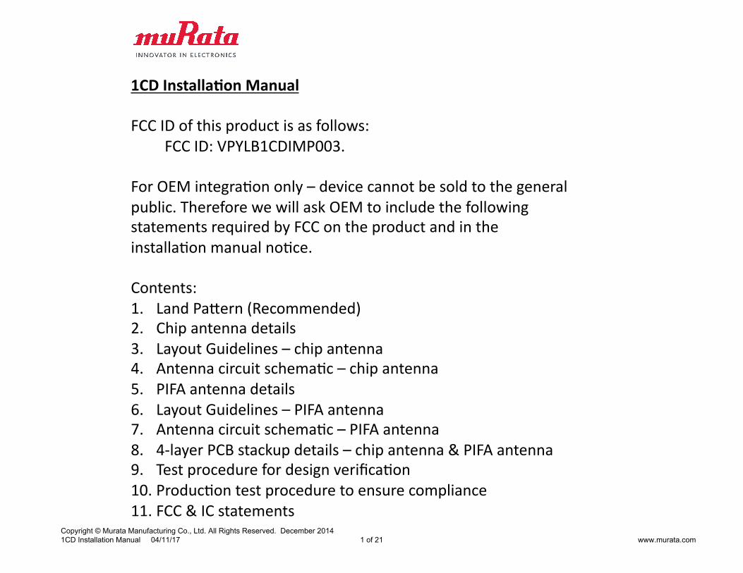
1CD$Installa+on$Manual$
FCC#ID#of#this#product#is#as#follows:##FCC#ID:#VPYLB1CDIMP003.#
For#OEM#integraDon#only#–#device#cannot#be#sold#to#the#general#public.#Therefore#we#will#ask#OEM#to#include#the#following#statements#required#by#FCC#on#the#product#and#in#the#installaDon#manual#noDce.#
Contents:#1.
Land#PaMern#(Recommended)#
2. Chip#antenna#details#3. Layout#Guidelines#–#chip#antenna#4. Antenna#circuit#schemaDc#–#chip#antenna#5. PIFA#antenna#details#6. Layout#Guidelines#–#PIFA#antenna#7. Antenna#circuit#schemaDc#–#PIFA#antenna#8. 4Ylayer#PCB#stackup#details#–#chip#antenna#&#PIFA#antenna#9. Test#procedure#for#design#verificaDon#10. ProducDon#test#procedure#to#ensure#compliance#11. FCC#&#IC#statements#
Copyright © Murata Manufacturing Co., Ltd. All Rights Reserved. December 2014 1CD Installation Manual 04/11/17 1 of 21 www.murata.com

2014/12/08�1.)Land)PaRern)(Recommended))�
Copyright © Murata Manufacturing Co., Ltd. All Rights Reserved. December 2014 1CD Installation Manual 04/11/17
2 of 21
www.murata.com

Copyright © Murata Manufacturing Co., Ltd. All Rights Reserved. December 2014 1CD Installation Manual 04/11/17
3 of 21
www.murata.com

Layout Guidelines: Chip Antenna This section provides required guidelines for PCB designs incorporating the 1CD module.
Figure 1 through Figure 4 show the four-layer 1CD wireless certification board. Refer to Figure 5 through Figure 7 for examples demonstrating good layout practices.
Copyright © Murata Manufacturing Co., Ltd. All Rights Reserved. December 2014 1CD Installation Manual 04/11/17
4 of 21
www.murata.com
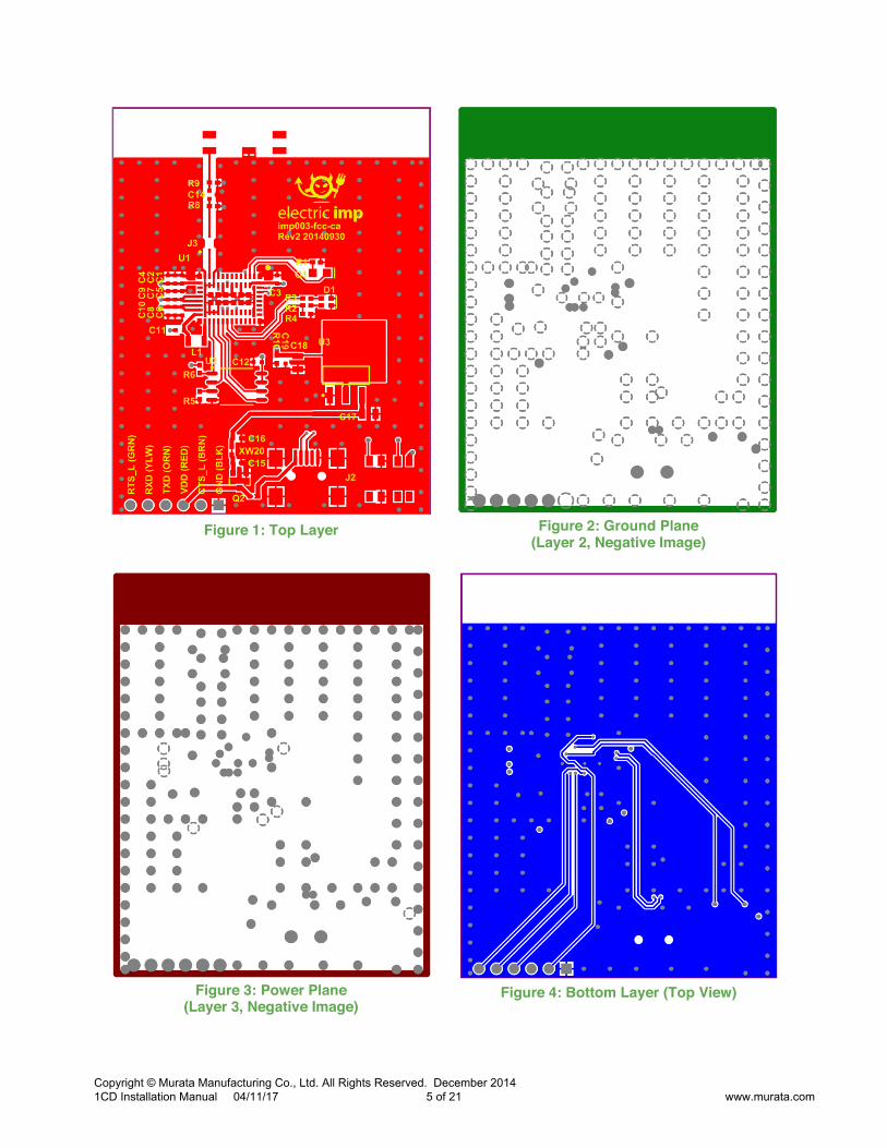
Figure 1: Top Layer
Figure 2: Ground Plane
(Layer 2, Negative Image)
Figure 3: Power Plane
(Layer 3, Negative Image)
Figure 4: Bottom Layer (Top View)
Copyright © Murata Manufacturing Co., Ltd. All Rights Reserved. December 2014 1CD Installation Manual 04/11/17
5 of 21
www.murata.com

Figure 5: RF_OUT Pad and Surrounding Ground Pads
Figure 5 shows the RF_OUT pad on the 1CD footprint. The RF_OUT pad is surrounded by ground pads; these should be tied together to form a ground reference around the end of the RF trace.
Tie together the ground pads surrounding the RF_OUT for ground reference
Copyright © Murata Manufacturing Co., Ltd. All Rights Reserved. December 2014 1CD Installation Manual 04/11/17
6 of 21
www.murata.com

Figure 6: RF Trace from Module to Antenna
Figure 6 shows the entire RF trace, from the 1CD module to the PIFA antenna. The RF trace must be a 50Ω ± 2Ω impedance controlled transmission line which is referenced to a solid, unbroken ground. The trace width and distance to the ground plane must be adjusted to achieve the target impedance. The trace must be shielded by applying stitching vias along the edge of the ground pour on both sides of the RF trace.
RF traces should be shielded by via stitching on both sides
RF traces must have constant impedance; the RF feed is a microstrip transmission line.
RF trace must be kept as short as possible.
Copyright © Murata Manufacturing Co., Ltd. All Rights Reserved. December 2014 1CD Installation Manual 04/11/17
7 of 21
www.murata.com
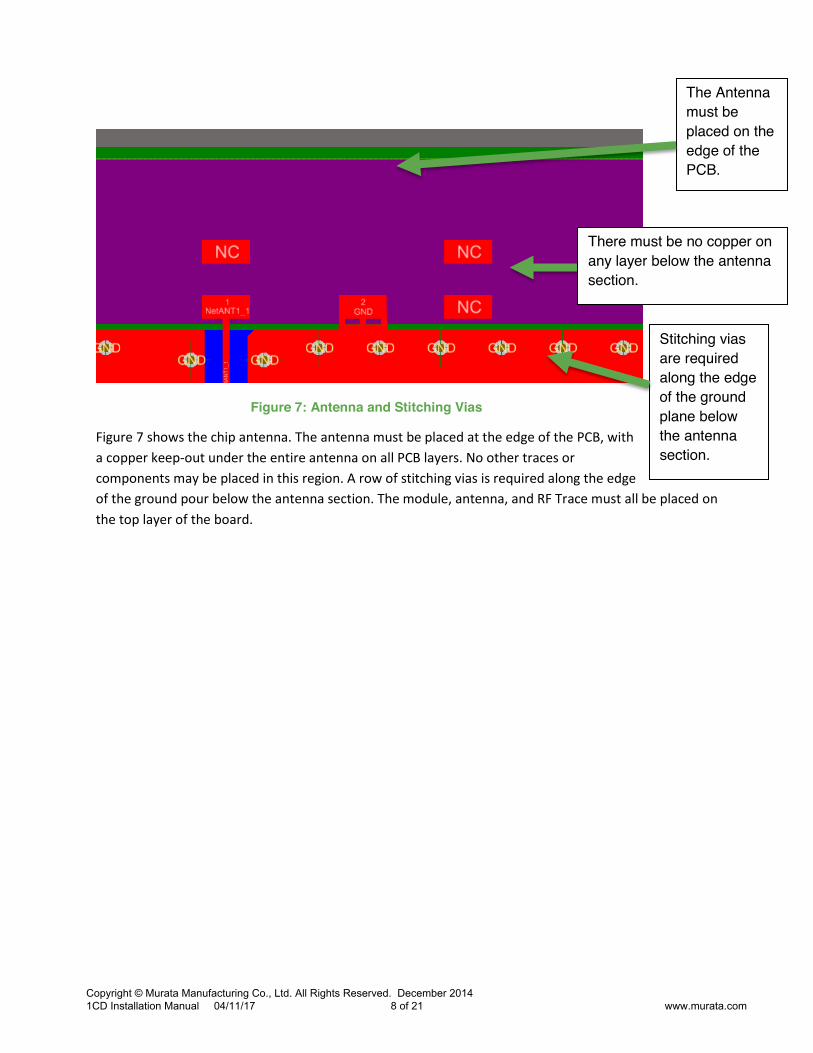
Figure 7: Antenna and Stitching Vias
Figure 7 shows the chip antenna. The antenna must be placed at the edge of the PCB, with a copper keep-out under the entire antenna on all PCB layers. No other traces or components may be placed in this region. A row of stitching vias is required along the edge of the ground pour below the antenna section. The module, antenna, and RF Trace must all be placed on the top layer of the board.
Stitching vias are required along the edge of the ground plane below the antenna section.
There must be no copper on any layer below the antenna section.
The Antenna must be placed on the edge of the PCB.
Copyright © Murata Manufacturing Co., Ltd. All Rights Reserved. December 2014 1CD Installation Manual 04/11/17
8 of 21
www.murata.com

Copyright © Murata Manufacturing Co., Ltd. All Rights Reserved. December 2014 1CD Installation Manual 04/11/17
9 of 21
www.murata.com

PAANT101PAANT102COANT1
PAC101PAC102
COC1 PAC201PAC202
COC2 PAC301PAC302
COC3
PAC401PAC402
COC4PAC501PAC502
COC5
PAC601
PAC602COC6
PAC701PAC702
COC7
PAC801
PAC802COC8
PAC901PAC902
COC9
PAC1001
PAC1002COC10PAC1101 PAC1102COC11
PAC1201 PAC1202COC12
PAC1402PAC1401 COC14
PAC1501PAC1502 COC15
PAC1601PAC1602 COC16
PAC1701PAC1702COC17
PAC1801
PAC1802COC18
PAC1901
PAC1902
COC19
PAD10KRPAD10ARPAD10AG PAD10KGCOD1
PAJ103 PAJ102 PAJ101PAJ104PAJ105PAJ106COJ1 PAJ20M4PAJ20M3
PAJ20M1 PAJ20M2PAJ201 PAJ202PAJ203 PAJ204 PAJ205PAJ20H2PAJ20H1 COJ2
PAJ304PAJ301
PAJ302PAJ303COJ3
PAL101 PAL102COL1
PAL201PAL202
COL2
PAQ10CPAQ10ECOQ1
PAQ203
PAQ202 PAQ201
COQ2
PAR101 PAR102COR1
PAR201 PAR202COR2PAR301 PAR302COR3
PAR401 PAR402COR4
PAR501PAR502COR5
PAR601PAR602COR6
PAR901PAR902 COR9
PAR1001PAR1002
COR10
PAS103PAS102
PAS104PAS101
COS1
PAS203 PAS202
PAS204 PAS201
COS2
PAU101PAU1014
PAU1023 PAU1036
PAU102PAU103PAU104PAU107 PAU106PAU105PAU1010PAU109PAU108PAU1013PAU1012PAU1011
PAU1026PAU1025PAU1024 PAU1029PAU1028PAU1027 PAU1032PAU1031PAU1030 PAU1033 PAU1034PAU1035
PAU1020PAU1021
PAU1017PAU1018PAU1019
PAU1016PAU1015
PAU1022 PAU1037
PAU1044
PAU1043
PAU1040PAU1041PAU1042
PAU1038PAU1039
PAU1053PAU1054 PAU1050PAU1051PAU1052 PAU1047PAU1048PAU1049 PAU1046 PAU1045
PAU1064PAU1063PAU1060 PAU1061PAU1062PAU1057PAU1058PAU1059PAU1055PAU1056PAU1073 PAU1074
PAU1067PAU1068 PAU1066PAU1065PAU1076PAU1075
PAU1070PAU1069PAU1072PAU1071
COU1
PAU205PAU206
PAU207
PAU208
PAU204PAU203
PAU202
PAU201
COU2 PAU304
PAU303PAU302PAU301
COU3
PAW101 PAW102
COW1
PAXW2001
PAXW2002 COXW20
PAC102PAC202 PAC302PAC402
PAC502PAC602
PAC702PAC802
PAC902PAC1002
PAC1202PAC1802PAC1902
PAR601
PAR1002
PAS202
PAU1015
PAU1018PAU1019PAU1020PAU1021
PAU1044PAU1045
PAU207
PAU208
PAU302
PAU304
PAU1017PAU1016
PAU108
PAR602
PAU1025
PAU201
PAC1102
PAL101
PAU1022
PAL102
PAU1024
PAJ202
PAU1043
PAJ203
PAU1042
PAS203
PAU1050
PAANT102
PAC101PAC201 PAC301PAC401
PAC501
PAC601
PAC701
PAC801
PAC901
PAC1001
PAC1101
PAC1201
PAC1401
PAC1501
PAC1601
PAC1701
PAC1801PAC1901
PAD10KGPAD10KR
PAJ101
PAJ205PAJ20M1 PAJ20M2
PAJ20M3 PAJ20M4
PAJ303PAJ304
PAQ201
PAR102
PAR402
PAR502
PAR902
PAR1001
PAS103
PAS104
PAU101PAU1010PAU1011PAU1013PAU1014
PAU1023 PAU1036
PAU1047PAU1049PAU1051PAU1053PAU1054
PAU1055PAU1056 PAU1057
PAU1065PAU1066PAU1067PAU1068PAU1069PAU1070PAU1071PAU1072PAU1073 PAU1074 PAU1075PAU1076
PAU204 PAU301
PAR301
PAU1030
PAR201PAR401
PAU1029PAU1026
PAU202
PAU1027
PAU205
PAC1402
PAJ301
PAL201
PAC1502
PAQ202
PAXW2001
PAD10AGPAR302PAD10ARPAR202
PAJ201
PAW102
PAR501 PAU203
PAQ10CPAU102 PAQ10EPAR101
PAU103
PAANT101
PAL202PAR901
PAU1041PAU1040PAU1039PAU1038PAU1037
PAU1035PAU1034PAU1033PAU1032PAU1031
PAU107
PAJ106
PAU1061
PAJ105
PAU1058
PAJ104
PAU1059 PAU1062PAU1060 PAU1063
PAU1048
PAJ102
PAU104
PAU1064
PAU1046
PAS101
PAU1052
PAJ302
PAU1012
PAU1028
PAU206
PAJ103PAQ203
PAW101
PAC1602
PAC1702
PAU303
PAXW2002
Copyright © Murata Manufacturing Co., Ltd. All Rights Reserved. December 20141CD Installation Manual 04/11/17
10 of 21 www.murata.com

Layout Guidelines: PIFA Antenna This section provides required guidelines for PCB designs incorporating the 1CD module.
Figure 1 through Figure 4 show the four-layer 1CD wireless certification board. Refer to Figure 5 through Figure 7 for examples demonstrating good layout practices.
Copyright © Murata Manufacturing Co., Ltd. All Rights Reserved. December 2014 1CD Installation Manual 04/11/17 11 of 21 www.murata.com

Figure 1: Top Layer Figure 2: Ground Plane (Layer 2, Negative Image)
Figure 3: Power Plane (Layer 3, Negative Image)
Figure 4: Bottom Layer (Top View)
Copyright © Murata Manufacturing Co., Ltd. All Rights Reserved. December 2014 1CD Installation Manual 04/11/17 12 of 21 www.murata.com

Figure 5: RF_OUT Pad and Surrounding Ground Pads
Figure 5 shows the RF_OUT pad on the 1CD footprint. The RF_OUT pad is surrounded by ground pads; these should be tied together to form a ground reference around the end of the RF trace.
Tie together the ground pads surrounding the RF_OUT to form a ground reference
Copyright © Murata Manufacturing Co., Ltd. All Rights Reserved. December 2014 1CD Installation Manual 04/11/17 13 of 21 www.murata.com

Figure 6: RF Trace from Module to Antenna
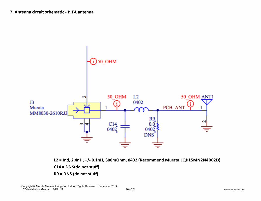
Figure 6 shows the entire RF trace, from the 1CD module to the PIFA antenna. The RF trace must be a 50Ω ± 2Ω impedance controlled transmission line which is referenced to a solid, unbroken ground. The trace width and distance to the ground plane must be adjusted to achieve the target impedance. The trace must be shielded by applying stitching vias along the edge of the ground pour on both sides of the RF trace.
RF traces should be shielded by via stitching on both sides
RF traces must have constant impedance; the RF feed is a microstrip transmission line.
RF trace must be kept as short as possible.
Copyright © Murata Manufacturing Co., Ltd. All Rights Reserved. December 2014 1CD Installation Manual 04/11/17 14 of 21 www.murata.com

Figure 7: Antenna and Stitching Vias
Figure 7 shows the PIFA antenna. The antenna must be placed at the edge of the PCB, with a copper keep-out under the entire antenna element on all PCB layers. No other traces or components may be placed in this region. A row of stitching vias is required along the edge of the ground pour below the antenna section; this ground pour, including the vias, is part of the antenna. The module, antenna, and RF Trace must all be placed on the top layer of the board.
Stitching vias are required along the edge of the ground plane below the antenna section.
There must be no copper on any layer below the antenna section.
The Antenna must be placed on the edge of the PCB
Copyright © Murata Manufacturing Co., Ltd. All Rights Reserved. December 2014 1CD Installation Manual 04/11/17 15 of 21 www.murata.com
Copyright © Murata Manufacturing Co., Ltd. All Rights Reserved. December 2014 1CD Installation Manual 04/11/17 16 of 21 www.murata.com

Copyright © Murata Manufacturing Co., Ltd. All Rights Reserved. December 2014 1CD Installation Manual 04/11/17 17 of 21 www.murata.com

9.$Test$procedure$for$design$verifica+on$
If#the#OEM#or#system#integrator#incorporates#the#1CD#module#into#their#final#product#and#wishes#to#reuse#the#1CD#module’s#FCC#cerDficaDon,#it#is#the#OEM/system#integrator’s#responsibility#to#perform#necessary#design#verificaDons#to#ensure#the#antenna#design#and#circuit#matches#those#specified#here.##
A#network#analyzer#could#be#used#to#measure#the#trace#impedance#and#dimensional#measurements#could#be#made#of#traces#to#confirm#the#design#was#implemented#per#the#specificaDon.#Radiated#tesDng#at#an#antenna#lab#can#also#be#performed#to#check#antenna#performance.#
Copyright © Murata Manufacturing Co., Ltd. All Rights Reserved. December 2014 1CD Installation Manual 04/11/17 18 of 21 www.murata.com
10.$Produc+on$test$procedures$for$ensuring$compliance$
If#the#OEM#or#system#integrator#incorporates#the#1CD#module#into#their#final#product#and#wishes#to#reuse#the#1CD#module’s#FCC#cerDficaDon,#it#is#the#OEM/system#integrator’s#responsibility#to#ensure#compliance#is#met#on#producDon#units.#
Incoming#inspecDon#of#the#PCB#should#be#performed#to#ensure#the#PCB#complies#with#laminate#material#spec,#50#Ohm#trace#impedance#spec,#PCB#stackup#spec,#antenna#dimensional#spec#and#copper#weight#spec.#Post#SMT,#inspecDons#should#be#made#to#ensure#the#stuffing#opDons#per#the#antenna#schemaDcs#are#followed.#
Copyright © Murata Manufacturing Co., Ltd. All Rights Reserved. December 2014 1CD Installation Manual 04/11/17
19 of 21
www.murata.com

FCC#Warning#!Notice!This!device!complies!with!Part!15!of!the!FCC!Rules.!Operation!is!subject!to!the!following!two!conditions:!(1)!this!device!may!not!cause!harmful!interference!and!(2)!this!device!must!accept!any!interference!received,!including!interference!that!may!cause!undesired!operation.!!Information!To!Be!Supplied!to!the!End!User!by!the!OEM!or!Integrator!The!following!regulatory!and!safety!notices!must!be!published!in!documentation!supplied!to!the!end!user!of!the!product!or!system!incorporating!an!adapter!in!compliance!with!local!regulations.!Host!system!must!be!labeled!with!“Contains!FCC!ID:!VPYLB1CDIMP003.!!This!1CD!module!is!to!be!used!only!for!mobile!and!fixed!application.!In!order!to!reVuse!the!1CD!module!FCC!approvals,!the!antenna(s)!used!for!this!transmitter!must!be!installed!to!provide!a!separation!distance!of!at!least!20cm!from!all!persons!and!must!not!be!coVlocated!or!operating!in!conjunction!with!any!other!antenna!or!transmitter.!If!antenna!is!installed!with!a!separation!distance!of!less!than!20cm!from!all!person!or!is!coVlocated!or!operating!in!conjunction!with!any!other!antenna!or!transmitter!then!additional!FCC!testing!and!certification!may!be!required.!EndVUsers!must!be!provided!with!transmitter!operation!conditions!for!satisfying!RF!exposure!compliance.!!!OEM!integrators!must!ensure!that!the!end!user!has!no!manual!instructions!to!remove!or!install!the!1CD!module.!Antennas!used!with!the!1CD!module!must!not!exceed!2.1dBi!gain!for!chip!antennas!or!2.24dBi!gain!for!PIFA!antennas.!!!!!!!!!!!!!!!!!!!!
Copyright © Murata Manufacturing Co., Ltd. All Rights Reserved. December 2014 1CD Installation Manual 04/11/17 20 of 21 www.murata.com

!
!
!
!
!
IC#Warning##Canada!LowVpower!licenseVexempt!radio!communication!devices!(RSSV210)!
a.!Common!information!Operation!is!subject!to!the!following!two!conditions:!
1.!This!device!may!not!cause!interference,!!and!
2.!This!device!must!accept!any!interference,!including!interference!that!may!cause!
undesired!operation!of!the!device.!
!
a.!Informations!communes!
Son!fonctionnement!est!soumis!aux!deux!conditions!suivantes:!
1.!Ce!dispositive!ne!peut!causer!des!interferences,!et!
2.!Ce!dispositive!doit!accepter!toute!interference,!y!compris!les!interferences!qui!
peuvent!causer!un!mauvais!fonctionnement!du!dispositive.!
!
Information!To!Be!Supplied!to!the!End!User!by!the!OEM!or!Integrator!
Modular!information!form!OEM!
Information!to!be!Supplied!to!the!End!User!by!the!OEM!or!Integrator!
The!following!regulatory!and!safety!notices!must!be!published!in!documentation!
supplied!to!the!end!user!of!the!product!or!system!incorporating!an!adapter!in!
compliance!with!local!regulations.!
Host!system!must!be!labeled!with!“Contains!IC:!772CVLB1CDIMP003”!
!
This!1CD!module!is!to!be!used!only!for!mobile!and!fixed!application.!In!order!to!reV
use!the!1CD!module!IC!approvals,!the!antenna(s)!used!for!this!transmitter!must!be!
installed!to!provide!a!separation!distance!of!at!least!20cm!from!all!persons!and!must!
not!be!coVlocated!or!operating!in!conjunction!with!any!other!antenna!or!transmitter.!
If!antenna!is!installed!with!a!separation!distance!of!less!than!20cm!from!all!person!
or!is!coVlocated!or!operating!in!conjunction!with!any!other!antenna!or!transmitter!
then!additional!IC!testing!and!certification!may!be!required.!EndVUsers!must!be!
provided!with!transmitter!operation!conditions!for!satisfying!RF!exposure!
compliance.!
!
OEM!integrators!must!ensure!that!the!end!user!has!no!manual!instructions!to!
remove!or!install!the!1CD!module.!Antennas!used!with!the!1CD!module!must!not!
exceed!2.1dBi!gain!for!chip!antennas!or!2.24dBi!gain!for!PIFA!antennas.!
!
Copyright © Murata Manufacturing Co., Ltd. All Rights Reserved. December 2014 1CD Installation Manual 04/11/17 21 of 21 www.murata.com
![Alternateur - Alternator - EUROREPAR...TOYOTA Avensis (T22) 1998ccm 1AC-FTV 1638109180 TOYOTA Corolla (_E11_)[1CD-FTV] 1638109180 TOYOTA Corolla (_E11_)[1CD-FTV] 1638109180 VOLVO S60](https://img.pdfslide.us/doc/110x75/5e8d8bc24f3a5f478d7422a1/alternateur-alternator-eurorepar-toyota-avensis-t22-1998ccm-1ac-ftv-1638109180.jpg)