Embed Size (px)
Citation preview
Graphene
Christopher OlsonUniversity of California, Santa Barbara
Materials 265November 10, 2008
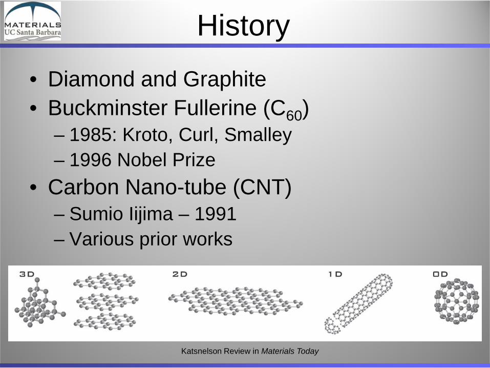
History
• Diamond and Graphite• Buckminster Fullerine (C60)
– 1985: Kroto, Curl, Smalley– 1996 Nobel Prize
• Carbon Nano-tube (CNT)– Sumio Iijima – 1991– Various prior works
Katsnelson Review in Materials Today
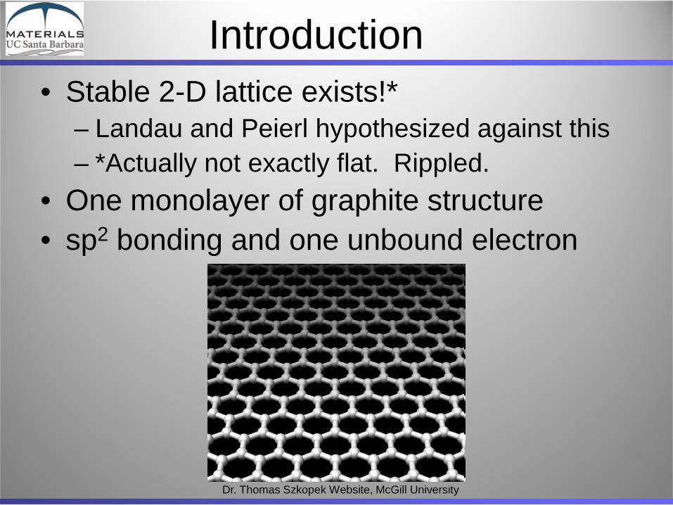
Introduction• Stable 2-D lattice exists!*
– Landau and Peierl hypothesized against this– *Actually not exactly flat. Rippled.
• One monolayer of graphite structure• sp2 bonding and one unbound electron
Dr. Thomas Szkopek Website, McGill University
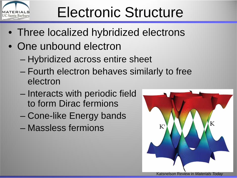
Electronic Structure• Three localized hybridized electrons• One unbound electron
– Hybridized across entire sheet– Fourth electron behaves similarly to free
electron – Interacts with periodic field
to form Dirac fermions– Cone-like Energy bands– Massless fermions
Katsnelson Review in Materials Today
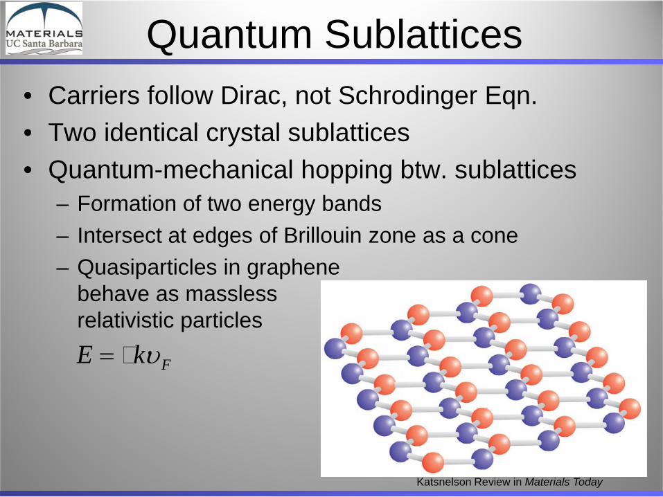
Quantum Sublattices• Carriers follow Dirac, not Schrodinger Eqn.• Two identical crystal sublattices• Quantum-mechanical hopping btw. sublattices
– Formation of two energy bands– Intersect at edges of Brillouin zone as a cone– Quasiparticles in graphene
behave as massless relativistic particles
Katsnelson Review in Materials Today
FkE υ=
Electronic Properties• Ultra-high mobility
– Routinely achieving 20,000 cm2/V·s– Order of magnitude better than Si– Three times higher than GaAs– World record 200,000 cm2/V·s set this January
• Ultra-low resistivity– Lower than silver (10-6 Ohm·cm)
• Tunneling probability is always unity
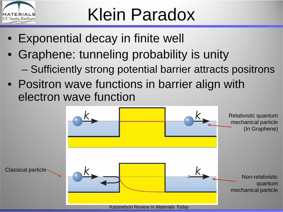
Klein Paradox• Exponential decay in finite well• Graphene: tunneling probability is unity
– Sufficiently strong potential barrier attracts positrons• Positron wave functions in barrier align with
electron wave function
Katsnelson Review in Materials Today
Classical particleNon-relativistic
quantummechanical particle
Relativistic quantummechanical particle
(In Graphene)
Consequences of Klein Paradox• Complete tunneling of electrons through
potential barriers twice electron’s rest energy• Single-layer graphene transistor will be
“always-on”, not “normally-on”• No applied bias will turn it off• Must create a bilayer graphene transistor
– Can strongly suppress normally-incident electron tunneling
Fabrication of Graphene• Mechanical exfoliation of graphite
– Method used by most people– By IBM and others to create first Graphene FET
• Heat up SiC to desorb Si– In UHV, heat up SiC to ~1300°C– Si atoms sublimate – Hexagonal carbon lattice (graphene) left behind
Processing of Graphene• CNTs have well-defined edges• Graphene has dangling bonds at edges• Difficult to cut manually into ribbons
– By confining electrons to narrow ribbon, open up small bandgap and make transistor possible
• Hope to get graphene nanoribbons (GNRs) 2 nm wide
• Silicon technology will die at around 20 nm
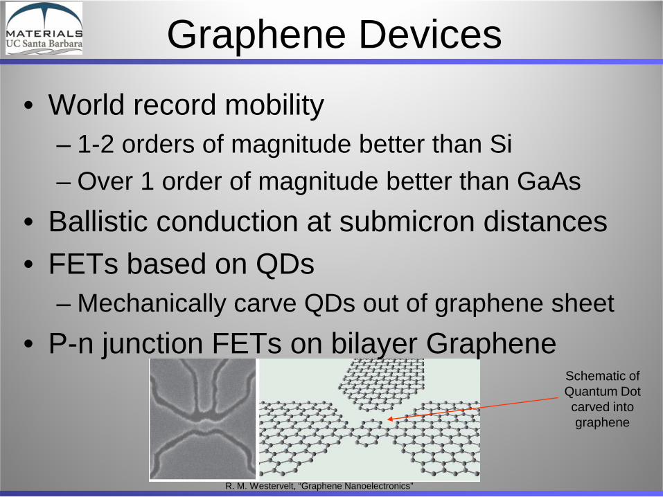
Graphene Devices• World record mobility
– 1-2 orders of magnitude better than Si– Over 1 order of magnitude better than GaAs
• Ballistic conduction at submicron distances• FETs based on QDs
– Mechanically carve QDs out of graphene sheet• P-n junction FETs on bilayer Graphene
R. M. Westervelt, “Graphene Nanoelectronics”
Schematic of Quantum Dot carved into graphene
Problems/Future Work• Difficult to make and process
– Can’t make large uniform wafers– Difficult to cut uniformly– Dangling bonds after cutting cause background
electrons to scatter• Switching speed too slow in prototype
graphene transistors
Other Applications• Gas Sensors
– Absorption of gas molecules dopes graphene– Measure change in resistivity
• THz Light Emitters– Human body invisible in THz frequency regime
• Superconductivity (proximity effect)• Magnetic/spintronics applications
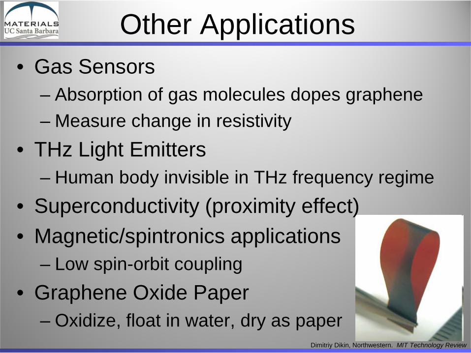
– Low spin-orbit coupling• Graphene Oxide Paper
– Oxidize, float in water, dry as paperDimitriy Dikin, Northwestern. MIT Technology Review
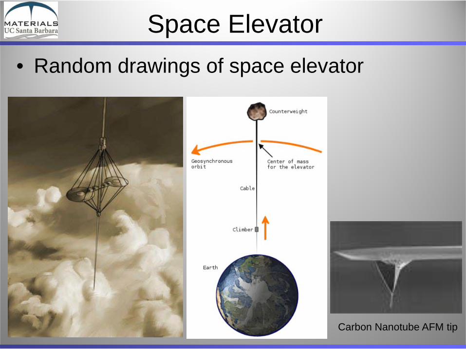
Space Elevator• Random drawings of space elevator
Carbon Nanotube AFM tip
Conclusions• Extremely new material system
– Production issues– Processing issues
• Excellent electrical and structural properties• Potential for small nano-scale (2 nm)
devices• Many potential applications• Will never replace Si, but has plenty of
potential niche markets
References• Mikhail I. Katsnelson, “Graphene: carbon in two dimensions,”
Materials Today, 2007.• A. K. Geim, K. S. Novoselov, “The rise of graphene,” Nature
Materials, 2007.• R. M. Westervelt, “Graphene Nanoelectronics,” Science vol. 320,
April 2008.• Dr. Thomas Szkopek Website, McGill University.
http://www.ece.mcgill.ca/~ts7kop/• Phil Schewe, “Graphene Speed Record,” American Institute of
Physics – Physics News Update• Dimitriy Dikin, et. al. “Preparation and characterization of graphene
oxide paper,” 2007. http://www.nature.com/nature/journal/v448/n7152/abs/nature06016.html
• Dimitriy Dikin website, Northwestern University• R. Colin Johnson, “IBM fabs graphene FETs,” EETimes.
Questions?