Embed Size (px)
Citation preview

GRAPHENE
Further Applications and Research
Team #3Phillip KellerKrista MelishMicheal JonesJames Kancewick
http://www.nanotech-now.com/images/Art_Gallery/AS-graphene.jpg

Overview
Introduction Graphene’s mechanical properties Graphene’s electrical properties
Carbon Vs Silicon Supercapacitors and Graphene Gas Detection using low-temperature reduced
graphene oxide sheets Ultrafast graphene photodetector Electronics and Magnetism of Patterned
Graphene Nanoroads General Conclusions

Introduction
Advances in electronics have been the result of the continuous miniaturization or ‘scaling’ of electronic devices, particularly of silicon-based transistors, that has led to denser, faster and more power-efficient circuitry.
http://www.scc.spokane.edu/_images/elect/circuit.gif
Charlier, J.-C., Blase, X., & Roche, S. Electronic and transport properties of nanotubes. Rev. Mod. Phys.
The realization of the approaching limits has inspired a worldwide effort to develop alternative device technologies. Some approaches involve spin-based devices, while others replace a key component of the device, the conducting channel, with carbon nanomaterials, which have superior electrical properties.

Introduction
Among these carbon nanomaterials is graphene. Graphene is a two dimensional allotrope of carbon arranged like a honeycomb structure made out of hexagons and plays an important role since it is the basis for the understanding of the electronic properties in other allotropes.
http://www.lbl.gov/Science-Articles/Archive/sabl/2007/Nov/assets/img/lrg/graphene_sheet.jpg

History of Graphene
Wallace in 1947 Created 2D structure to help in the understanding
of 3D Graphite Single layers of graphite grown epitaxially on
metallic substrates in the 1970s Tightly bound to substrate, distorted properties
Term “graphene” coined in 1987 2004, Geim and Novoselov mechanically exfoliated
sheets of graphene from graphite Transferred to charge neutral silicon substrate First successful electrical properties measured
Geim, A. K. & MacDonald, A. H. (2007). "Graphene: Exploring carbon flatland". Physics Today.

A Closer Look at Graphene
2D hexagonal carbon crystal lattice Infinite boundaries Actual 2D structure is debatable
Graphene sandwich Thermal effects
Naturally occurring Multilayer in graphite Nanospecs in soot from exhaust
Currently one of the most researched materials Unique physical and electrical
properties Wide array of potential uses
http://www.nanotechnow.com/images/Art_Gallery/ASgraphene.jpg
Ziegler, K., Robust transport properties in graphene. Phys. Rev. Lett.

Graphene Mechanical Properties Breaking strength 200
times greater than steel
Youngs modulus of ~ 1 tPa
Incredible rigidity lends themselves to nanoscale pressure sensors Nanoscopic graphene
flakes bend with increasing pressure which alters their electrical conductivity which can be related to the pressure
John Scott Bunch. Mechanical and Electrical Properties of Graphene. Cornell University 2008.
http://www.kinectrics.com/images/CableSpan.JPG
Thermal properties exceed those of diamond Excellent conductor of
heat Phonon dominated
although it can be shown that at certain conditions the electrical portion is significant

Graphene Electrical Properties
Anomalous Quantum Hall Effect Quantization of the Hall
effect Dirac fermions
Carriers have zero effective mass
Room temperature electron mobility of 15,000 cm2/V*s Theoretically higher
conductivity at room temp than silver, but unknown forces are limiting
Possible optical phonon scattering from attached substrate
Charlier, J.-C., Blase, X., & Roche, S. Electronic and transport properties of nanotubes. Rev. Mod. Phys.
http://www.atwillett.com/lighting_pictures/lightningbolt_closeup.jpg
Both P and N-type transistors have been created
Recent announcement by IBM that graphene transistor was operated at a terahertz frequency
Tunable band gap from 0 to 0.25 eV
Excellent conductivity makes graphene ideal for electrical leads in sensors/capacitors or use in touch screens because of its mechanical strength
Graphene ribbons have tunable electrical conductivity depending on the shape

Electrical Component: Transistor A transistor's operation speed depends on the
size of the device — smaller devices can run faster — and the speed at which electrons travel in it. This size dependence has been one of the major driving forces for making ever smaller silicon transistors.
The Consortium of International Semiconductor Companies in its 2001 International Technology Roadmap for Semiconductors projected that transistors have to be smaller than 9 nanometers by 2016 in order to continue the performance trend.
Charlier, J.-C., Blase, X., & Roche, S. Electronic and transport properties of nanotubes. Rev. Mod. Phys.

Carbon vs. Silicon
Figure (a) is Intel’s 45 nm silicon transistor which uses a Hafniun based dielectric.
Figure (b) is a wafer of the 45 nm transistors photographed with a dime. The processors incorporate 410 million transistors for each dual core chip, and 820 million for each quad core chip.http://www.intel.com/pressroom/kits/45nm/
photos.htm.

Carbon vs. Silicon
Graphene could offer a way forward. As well as being extremely thin and a semiconductor, electrons move through graphene at extremely high speeds.
http://mayang.com/textures/Manmade/images/Plastics%20and%20Related/electronic_circuit_board_9131073.JPG
Geim, A. K. & Novoselov, K. S. The rise of graphene. Nature Mater.
The cutting edge of silicon-based transistors is at 32 nanometers.
Graphene has the potential to fabricate transistors only a few atoms across. British researchers have unveiled the world’s smallest transistor, which measures one atom thick and ten atoms across. This is in the sub-10 nanometer range

Performance Characteristics for Carbon-Based Transistor
Ambipolar transfer characteristics [current versus gate voltage]: drain bias increases from –0.1 V to –1.1 V in –0.2 V steps. Red line represents -0.1 V and the pink line is -1.1 V. Step size is -0.2 V
Left Inset: Schematic of the band structure of a Schottky barrier semiconducting carbon nanotube in a field effect transistor under negative gate bias. Holes areinjected from the source [S].
Right Inset: Schematic of the band structure of a Schottky barrier semiconducting carbon nanotube in a field effect transistor under positive gate bias. Electrons areinjected from the drain [D].
Anantram, M. P. & Leonard, F. Physics of carbon nanotube electronic devices. Rep. Prog. Phys.

Electrical Component: Supercapacitors
Supercapacitors are energy storage systems that are able to store and deliver energy at relatively high rates. They are able to store and deliver energy beyond
those accessible by batteries. This is because the mechanism of energy storage is the simple charge-separation at the electrochemical interface between the electrode and the electrolyte.
Chen, Y. et al. Supercapacitor Devices Based on Graphene Materials. J. Phys. Chem. C 2009
>http://www.johnhenryshammer.com/WOW/willWebPics/battery/superCap.jpg
http://carolinepond.files.wordpress.com/2008/12/energizer-bunny.jpg

Supercapacitors
An advantage for supercapacitors is that they have several orders of magnitude higher energy density than that of conventional dielectric capacitors. Furthermore, the deficiencies of other power sources,
such as batteries and fuel cells, could be complemented by supercapacitors, owning to their long cycle life and rapid charging and discharging at high power densities.
Chen, Y. et al. Supercapacitor Devices Based on Graphene Materials. J. Phys. Chem. C 2009
+http://www.johnhenryshammer.com/WOW/willWebPics/battery/superCap.jpg
http://carolinepond.files.wordpress.com/2008/12/energizer-bunny.jpg

Supercapacitors
When the practical use of electrochemical capacitors for the storage of electrical charge was demonstrated and patented by General Electric, supercapacitors have generated great interest for a wide and growing range of applications such as:
Kotz, R.; Carlen, M. Electrochim. Acta 2000, 45, 2483.
http://i.thisislondon.co.uk/i/pix/2008/07/general-electric-415x275.jpg
Links to pictures are in notes
Load cranes Forklifts Electric vehicles Electric utilities Factory power
back up

Supercapacitors
Different materials such as various carbon materials, mixed metal oxides, and conducting polymers have been used as supercapacitor electrode materials.
http://www.easycalculation.com/chemistry/elements/images/carbon.jpg
Pandolfo, A. G.; Hollenkamp, A. F. J. Power Sources 2006, 157, 11.
Particularly carbon, in its various forms, has been used as electrode materials of supercapacitors, aiming at high specific capacitance together with high power density.

Supercapacitors
Although porous carbon materials have high specific surface area, the low conductivity of porous carbon materials is limiting its application in high power density supercapacitors. Carbon nanotubes (CNTs), with excellent
electrical conductivity and high surface areas, have been fabricated for supercapacitors since 1997.
Diederich, L.; Barborini, E.; Piseri, P.; Podesta, A.; Milani, P. Appl. Phys. Lett. 1999, 75, 2662.
https://www.opassoap.com/opasstore/media/catalog.jpg
http://www.t12.lanl.gov/home/afv/nanotube.singleframe.begin.gif

Supercapacitors
However, CNT-based supercapacitors have not met the expected performance; one possible reason is probably due to the observed contact resistance between the electrode and current collector. Hence, many studies have
focused on the morphology of the carbon materials to boost the performance of the capacitor, such as growing CNTs directly on bulk metals to eliminate the contact resistance.
http://www.deskpicture.com/DPs/Technology/CircuitBoard_2.jpg
http://fc05.deviantart.net/fs24/f/2008/018/e/3/Smoke_Stock_002_by_mross5013.jpg
Shaijumon, M. M.; Ou, F. S.; Ci, L. J.; Ajayan, P. M. Chem. Commun. 2008, 2373.

Supercapacitors
Graphene is emerging as a unique morphology carbon material with potential for electrochemical energy storage device applications due to its superb characteristics of chemical stability, high electrical conductivity, and large surface area.
Fig (a). Schematic diagram of graphene-based supercapacitor device
Chen, Y. et al. Supercapacitor Devices Based on Graphene Materials. J. Phys. Chem. C 2009
Recently, it has been proposed that graphene should be a competitive material for supercapacitor application. Graphene with less agglomeration should be expected to exhibit higher effective surface area and thus better supercapacitor performance.

GAS DETECTION USING LOW-TEMPERATURE REDUCED GRAPHENE OXIDE SHEETS
By
Ganhua lu
Leonidas E. Ocola
Junhong Chen

Gas Detection using reduced graphene sheets
high-performance gas sensors made of partially reduced graphene oxide sheets
obtained through low-temperature step annealing at 300 °C in argon flow at atmospheric pressure
Was tested with low concentration NO2
W. Frank, J. Vac. Sci. Technol. B 25, 2558 2007
http://www.engineerlive.com/media/images/large/large_1112_D12_Image.JPG

Background
The 2D structure of graphene makes every carbon atom a surface atom so that electron transport can be highly sensitive to adsorbed molecules.
Mechanically exfoliated graphene has demonstrated a potential ability to detect gases down to the single molecular level
The gas sensing mechanism of graphene is generally attributed to the adsorption/desorption of gaseous molecules which act as donors or acceptors on the graphene surface, leading to changes in the conductance of grapheneS. Novoselov, Y. Zhang, I. V. Grigorieva, and A. A. Firsov, Science 306,
666 2004.
http://c0378172.cdn.cloudfiles.rackspacecloud.com/graphene-interconnects.jpg

Chemically Reduced Graphene Oxide using Hydrazine
Has been used for the detection of acetone, warfare agents, and explosive agents at parts per billion concentrations
Using Hydrazine for sensor fabrication involves toxic chemicals and introduce extra nitrogen functional groups which may slow the response of the sensor.
Yang, A. Velamakanni, G. Bozoklu, S. Park, M. Stoller, R. D. Piner, S. Stankovich, I. Jung, D. A. Field, C. A. Ventrice, Jr., and R. S. Ruoff, Carbon 47, 145 2009.
http://2.bp.blogspot.com/_VyTCyizqrHs/SRoCXZgYZxI/AAAAAAAABoU/64fpjTGIJjw/s1600-h/graphene_sheet.jpg
Below is graphene prepared with Hydrazine

Modified Hummers Method
Was used for the creation of the graphene oxide sheets used for sensors
Graphite is first synthesized by oxidative treatment Then is exfoliated in water to produce suspension
of single graphene oxide sheets For a detailed explanation of Hummer’s method please
visit http://pubs.acs.org/doi/abs/10.1021/ja01539a017
Park, J. An, R. D. Piner, I. Jung, D. Yang, and R. S. Ruoff, Chem. Mater. 20, 6592 2008.
http://www.air-intakes.net/Hummer.gif
Chemistry
http://www.physics.umanitoba.ca/~tapash/nano/molecule-graphene.jpg

Fabrication of the Sensing Device
The graphene oxide was suspended with Au interdigitated electrodes. Both finger width and
interfinger spacing of 1 µm
Drops of the graphene oxide suspension where then placed on the wafer.
H. Lu, L. E. Ocola, and J. H. Chen, J. Nanomater. 2006, 60828 2006
http://www.physics.upenn.edu/yodhlab/images/research_CMP_Solubilization.jpg

The Fabrication of the Electrodes The Au interdigitated electrodes
were fabricated using electron-beam lithography on a Silicon wafer.
http://www.cnst.nist.gov/nanofab/nanofab_equipment/images/leica.jpg

The Sensor
FIG. 1. Color online SEM image of a GO sheet bridging two neighboring Au fingers of an interdigitated electrode. Gases are detected by measuring the change in the current while applying a constant dc bias to the device.
Leonidas E. Ocola, et al, Gas detection using low-temperature reduced graphene oxide sheets 2009 American Institute of Physics, 2009
Figure obtained from article

How it works
When different gases absorb to it the electrical conductance of the Graphene Oxide changes and is used to detect certain gases as extremely low concentrations
For this experiment it was tested using NO2
After the annealing process at 300 °C absorption sites opened allowing for low concentrations of N02 to cause a change in the resistance of the sensor.
Gomez-Navarro, R. T. Weitz, A. M. Bittner, M. Scolari, A. Mews, Nano Lett. 7, 3499 2007.
http://www.durawear.com/images/catalog/live/imageLibrary/35314ECE1517585314A3B395639BAE23M.jpg

The sensor
Can detect a single atom of N02 which is shown in the figure below
When the N02 binds to thegraphene the electrical properties change and this canbe detected
http://www.rsc.org/images/GrapheneNO2-250_tcm18-95542.jpg
24H. A. Becerril, J. Mao, Z. Liu, R. M. Stoltenberg, Z. Bao, and Y. Chen, ACS Nano 2, 463 2008.

Problems that need further research
Exploring methods to enhance sensor recovery Currently it takes the sensors
longer than 30 minutes to recover under normal conditions
Methods to be explored Low temperature heating UV illumination
Leenaerts, B. Partoens, and F. M. Peeters, Phys. Rev. B 77, 125416 2008
http://dkamhi.com/uv%20600x450.jpg

ULTRAFAST GRAPHENE PHOTODETECTOR
By
Fengnian Xia
Thomas Mueller
Yu-ming Lin
Alberto Valdas-Garcia
Phaedon Avouris
http://img.directindustry.com/images_di/photo-g/photodetector-27819.jpg

Graphene’s photonic abilities
Ability to absorb ~ 2% of incident light over a broad wavelength
Multiple graphene layer absorb additively
The absorption range of a system can be tuned by changing the Fermi energy using an external gate field
Wang, F. et al. Gate-variable optical transition in graphene. Science 320, 206–209 (2008).
http://www.nanotech-now.com/images/NANOIDENTPhotodetectorFunction300.jpg

Field-Effect Transistors (FETs)
Zero bandgap,large-area single or few-layers of graphene as FETs are used in this paper
Internal fields are shown in this paper to produce an ultrafast photocurrent response in graphene
http://rocky.digikey.com/weblib/ST%20Micro/Web%20Photos/New%20Photos/POWERSO-10jpg.jpg
http://images.iop.org/objects/phw/news/thumb/14/2/10/graph1.jpg
Xia, F. et al. Photocurrent imaging and efficient photon detection in a graphenetransistor. Nano Lett. 9, 1039–1044 (2009).

Applications of Photonic applications
High-speed optical communications Interconnects Terahertz detection Imaging Remote sensing Surveillance Spectroscopy
http://www.sflp.co.uk/xhtml-css/images/surveillance1.jpg
http://www.delen.polito.it/var/
http://www.eecs.umich.edu/optics/html/pics/optics-main4.jpg
Geim, A. K. & Novoselov, K. S. The rise of graphene. Nature Mater. 6, 183–191 (2007).

SEM and optical images of High-bandwidth graphene photodetector
The graphene shown here has two to three layers Two types of wirings are shown: ground–signal (G–S) and ground–signal–
ground(G–S–G) Optical bottom left, SEM is the remaining black and white image
Chuang, S. Physics of Optoelectronic Devices (Wiley, 1995).
Figure obtained from article
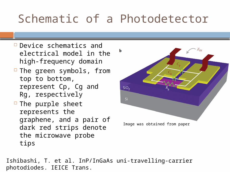
Schematic of a Photodetector
Device schematics and electrical model in the high-frequency domain
The green symbols, from top to bottom, represent Cp, Cg and Rg, respectively
The purple sheet represents the graphene, and a pair of dark red strips denote the microwave probe tips
Ishibashi, T. et al. InP/InGaAs uni-travelling-carrier photodiodes. IEICE Trans.Electron. E83-C, 938–949 (2000).
Image was obtained from paper

The High speed Impedance
Impedance – is an important relation of the physical set up of the device in order to filter out the low frequency signals from registering on the device
This equation is what sets the gate bias for the photodetector. Ryzhii, V., Mitin, V., Ryzhii, M., Ryabova, N. & Otsuji, T. Device model for
graphene nanoribbon phototransistor. Appl. Phys. Exp. 1, 063002 (2008).

Photodetectors
Magnitude of the photocurrent is strong function of the location of the optical illumination and also on the gate bias which are calculated with the impedance equation
The figure to the right displays the absolute a.c. photoresponse as a function of light intensity modulation frequency up to 26 GHz with the gate bias varying from -40 to 80V
Meric, I. et al. Current saturation in zero-bandgap, top-gated graphene fieldeffecttransistors. Nature Nanotech. 3, 654–659 (2008).

Future research for Photodetectors
Enhancing the ability of the photodetectors to detect a broader light position.
The incorporation of photodetectors into use
Large scale manufacture of photodetectors
Use of photodetectors as transistors
http://research.microsoft.com/en-us/um/people/jpwang/full_images/led_brdf.jpg

ELECTRONICS AND MAGNETISM OF PATTERNED GRAPHENE NANOROADS
By Abhishek K. Singh
Boris I. Yakobson http://www.blogcdn.com/www.engadget.com/media/2010/04/graphene-20100402.jpg

Nanoroads
Carving Graphene roads out of fully hydrogenated carbon sheets create “Nanoroads”
This is a method in which the individual characteristics depending upon the zigzag and orientation can be studied to their corresponding affects.
Graphane is shown to the left and is full hydrogenated graphene
Chen, Z.; Lin, Y.; Rooks, M. J.; Avouris, P. Physica E 2007, 40, 228.
ceramics.org/ceramictechtoday/tag/graphene/

Graphene Vs. Graphane
http://www.afs.enea.it/project/cmast/Documenti/web/foto/Pulci_fig1.jpg

Papers Concept
Can hydrogenation be used to form geometrical areas, such as “roads” of pristine graphene with the desired electronic properties?
This would be done to receive the same electrical properties of graphene nanoribbons without having to cut the graphene.
http://images.google.com/imgres?imgurl=http://ceramics.org/ceramictechtoday
Hod, O.; Barone, V.; Peralta, J. E.; Scuseria, G. E. Nano Lett. 2007, 7, 2295.

Armchair and Zigzag orientation
Relaxed structure of (a) armchair nanoroad (b) zigzag nanoroad
Na and Nz are the width measured by the number of pristine sp^2 carbon dimer-lines or zigzag chains respectively
Son, Y.; Cohen, M.; Louie, S. Nature 2006, 444, 347.
Figure obtained from article

Conclusions of Paper
In order for the nanoroads to be well defined, the sharpness of the interfaces between hydrogenated and pristine graphene is important.
Conducting and semiconducting nanoroads can in principle be patterned on a graphene by hydrogenation
Dewar, M. J. S.; Dougherty, R. C. The PMO Theory of Organic Chemistry, 1st ed.; Plenum: New York, 1975

Conclusions of Paper Continued Antiferromagnetic state is
semiconducting, the ferromagnetic state is metallic with a width-independent moment of 0.80 μB/unit cell
The possibility of having metallic and semiconducting roads on the same planar geometry can be an advantage in certain applications
Dewar, M. J. S.; Dougherty, R. C. The PMO Theory of Organic Chemistry, 1st ed.; Plenum: New York, 1975

Further Research
Achieve a rough patterns and directionality by the masked exposure to a reagent transforming sp2 carbon into sp3, while further energy minimization of the interface
The magnetism in wider nanoroads should display better stability and this should be researched
Applications of this technology also is in need for research

Potential Issues
An inability to produce graphene of consistent sizes and consistent electronic properties.
Difficulty integrating graphene into electronic devices using processes suitable for volume production.
High electrical resistance that produces heating and energy loss at junctions between graphene and the metal wires connecting them.
Anantram, M. P. & Leonard, F. Physics of carbon nanotube electronic devices. Rep. Prog. Phys.
http://www.thelocal504.com/wpcontent/uploads/2009/05/broken_computer.jpg

Further Research
Incorporating diamond as a semiconductor in high-temperature, high-power applications.
Accurate mass production techniques. Essentially developing an entire
electronic computing system with carbon-based electronics.
http://www.absolutediamonds.co.za/images/diamonds.jpg
http://www.deskpicture.com/DPs/Technology/CircuitBoard_2.jpg
http://www.cnanorhonealpes.org/IMG/gif/BuckyTube_s.gif
→ ←

Conclusion
Bearing excellent material properties, such as high current-carrying capacity and thermal conductivity, graphene and other carbon based allotropes are ideally suited for creating components for semiconductor circuits and computers. Its planar geometry allows the fabrication of electronic devices and the tailoring of a variety of electrical properties. Because it is only one-atom thick, it can potentially be used to make ultra-small devices and further miniaturize electronics.