Embed Size (px)
Citation preview
NPL Management Ltd - Internal
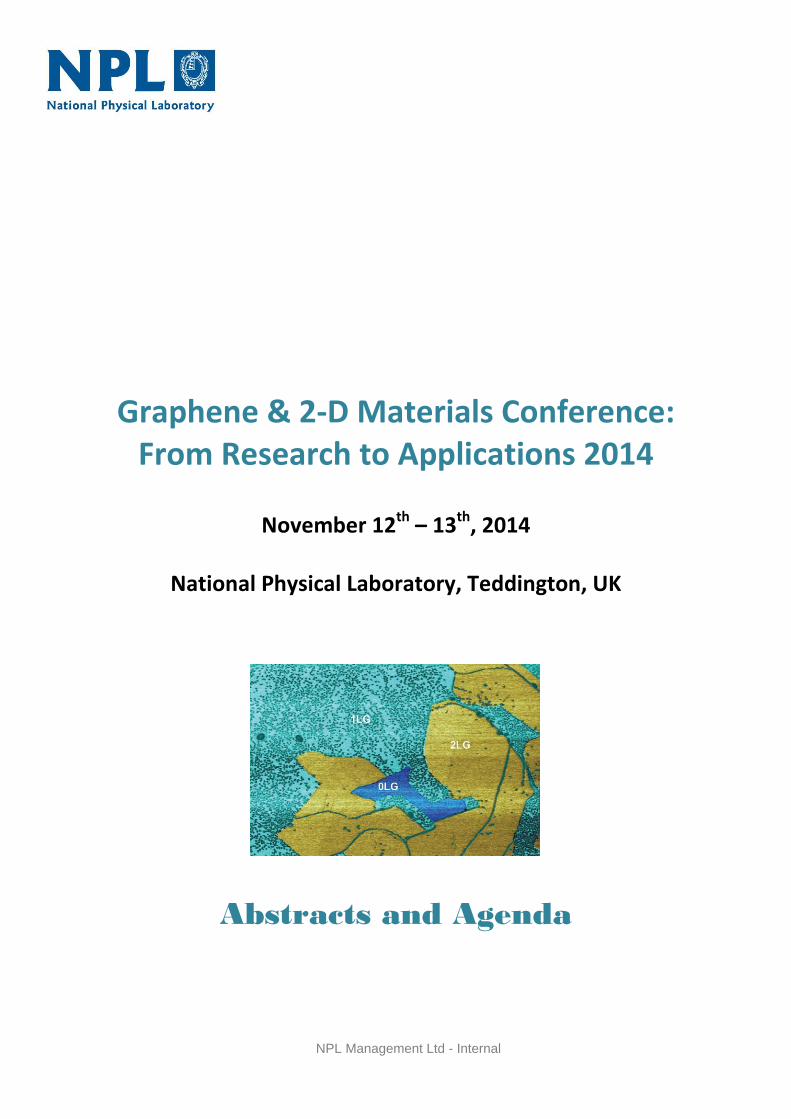
Graphene & 2-D Materials Conference: From Research to Applications 2014
November 12th – 13th, 2014
National Physical Laboratory, Teddington, UK
Abstracts and Agenda
NPL Graphene & 2-D Materials Conference – From Research to Applications 2014
12th – 13th November, 2014 NPL, Teddington, UK
NPL Management Ltd - Internal
Welcome to NPL Dear Colleagues, The organising committee takes great pleasure in welcoming you to the second Graphene Conference: From Research to Applications taking place at the National Physical Laboratory in Teddington. This two day conference will address new concepts of graphene and progress in understanding technology, physics and metrology. The event will also discuss how best to translate the knowledge gained in science laboratories to commercial applications. Presentations will be given by key international experts from industry and academia, in particular the members of the Graphene Flagship and EMRP GraphOhm. Ten years after its original discovery, the field of graphene research and development is gaining maturity. A significant number of start-ups have emerged and also larger established companies are starting to embrace this new technology. Metrology will play a key in establishing the value chain for graphene by developing traceable characterisation tools and formulating much-needed standards. We truly hope that this symposium serves as an international platform for fruitful communication between the scientific and industrial communities. Bridging the translational gap, sometimes referred to as the 'valley of death', between research and industry is a major challenge, but one that NPL is well positioned to meet. The organisers hope you will take the opportunity to visit the diverse range of specialised laboratories at NPL and get a chance to interact with our scientists directly. We would like to thank the exhibitors for their participation and would like to acknowledge the financial support of the UK National Measurement Office (NMO). Kind Regards, Organising committee
NPL WiFi details: Search for “guest access” – User name: guest Password: teddington
NPL Graphene & 2-D Materials Conference – From Research to Applications 2014
12th – 13th November, 2014 NPL, Teddington, UK
NPL Management Ltd - Internal
Oral Presentations - Abstracts
Day 1 – Wednesday, November 12th
Section 1 – Opening Remarks
Invited Speaker 1.1: James Baker, Business Director, National Graphene Institute, The University of Manchester Graphene at Manchester – The Route to Commercialisation
Invited Speaker 1.2: Tomas Löfwander, Docent/Associate Professor, Department of Microtechnology and Nanoscience, Chalmers University of Technology, Sweden & Chairman of Flagship Graphene
Bushy House, the first home of NPL
NPL Graphene & 2-D Materials Conference – From Research to Applications 2014
12th – 13th November, 2014 NPL, Teddington, UK
NPL Management Ltd - Internal
Section 2 – Large Scale Growers & Characterisation
2.1 Dr. Keith Paton, Project Leader – Graphene, Thomas Swan & Co. Ltd., Consett, UK
In situ spectroscopic metric to determine size and thickness of liquid-exfoliated graphene
Claudia Backes,1 Keith Paton,1,2 Damien Hanlon,1 Jonathan N. Coleman1
1 School of Physics and CRANN, Trinity College Dublin, D2, Dublin, Ireland
2 Thomas Swan and Company Limited, Rotary Way, Consett DH8 7ND, UK.
Many applications of graphene require the dispersion and exfoliation of graphite in the
liquid phase. While this can be achieved by intercalation or oxidation, the simplest way is
the direct exfoliation of graphite in suitable solvents or aqueous surfactant solutions (liquid
exfoliation) to produce defect-free few layer graphene. Originally, this work focused on
using sonication to provide energy to overcome the van der Waals interaction between the
individual sheets. Recently, a highly scalable production technique based on shear
exfoliation was demonstrated giving access to large quantities of graphene in liquids.[1]
However, the resultant material is highly polydisperse with regard to lateral dimensions and
thickness. While size selection techniques have been demonstrated for liquid-exfoliated
graphene, evaluating the effectiveness of these is extremely tedious, as currently size and
thickness needs to be determined by statistical microscopic analysis (both TEM and AFM).
An in-situ spectroscopic metric to determine size and thickness is therefore of great
importance.
We have previously shown for liquid-exfoliated MoS2[2] that extinction, absorbance and
scattering spectra distinctively changes as a function of size and thickness due to edge and
confinement effects. This allows for concentration, lateral dimensions and number of layers
to be determined in a single extinction measurement. We now demonstrate that similar
metrics are available for liquid-exfoliated graphene. In addition, we propose simple metrics
based on Raman spectra of size-selected graphene in restacked films to quantify size and
thickness on the foundation of the G-band width and changes in the 2D band shape.
These metrics greatly facilitate the preparation of dispersions with pre-defined properties
and are the ideal foundation to develop new, scalable size selection protocols.
1. K. R. Paton, E. Varrla, C. Backes, ... J. N. Coleman, Scalable production of large quantities of defect-free few-layer graphene by shear exfoliation in liquids. Nat Mater 2014, 13 (6), 624-630.
2. C. Backes, ... J. N. Coleman, Using Edge and Confinement Effects for in situ Determination of Size and Thickness of Liquid-Exfoliated Nanosheets. Nat. Commun. 2014, 5, 4576.
NPL Graphene & 2-D Materials Conference – From Research to Applications 2014
12th – 13th November, 2014 NPL, Teddington, UK
NPL Management Ltd - Internal
2.2 Stefan Schwarz, Department of Physics & Astronomy, University of Sheffield
Two-dimensional metal-chalcogenide films in microcavity structures
S. Schwarz1, S. Dufferwiel1, P. M. Walker1, F. Withers2, A. Trichet3, M. Sich1, F. Li1, E. A. Chekhovich1, D. N. Borisenko4, N. N. Kolesnikov4, K. S. Novoselov2, M. S. Skolnick1, J. M. Smith3, D. N. Krizhanovskii1, A. I. Tartakovskii1
1Department of Physics and Astronomy, University of Sheffield
2School of Physics and Astronomy, University of Manchester
3Department of Materials, University of Oxford
4Insitute of Solid State Physics, Russian Academy of Sciences, Chernogolovka
Quasi-two-dimensional (2D) films of layered metal-chalcogenides have attractive
optoelectronic properties. However, photonic applications of thin films may be limited
owing to weak light absorption and surface effects leading to reduced quantum yield.
Embedding 2D films in photonic structures will permit to overcome these drawbacks. Here
we present tunable microcavities with embedded monolayer molybdenum disulphide
(MoS2) or few monolayer gallium selenide (GaSe) films. The microcavity is formed by one
planar and one concave-shaped distributed Bragg reflector, leading to a confined cavity
are achieved.
We observe significant modification of spectral and temporal properties of
photoluminescence (PL) of 2D films. PL is emitted in spectrally narrow and wavelength-
tunable cavity modes with quality factors up to 7000 and life-time shortening with a Purcell
factor of 10 is achieved. This work will pave the way to microcavity-enhanced light-emitting
devices based on layered 2D materials and their heterostructures, and also opens
possibilities for cavity QED in a new material system of van der Waals crystals.
2.3 Nicholas D. Kay, Physics,
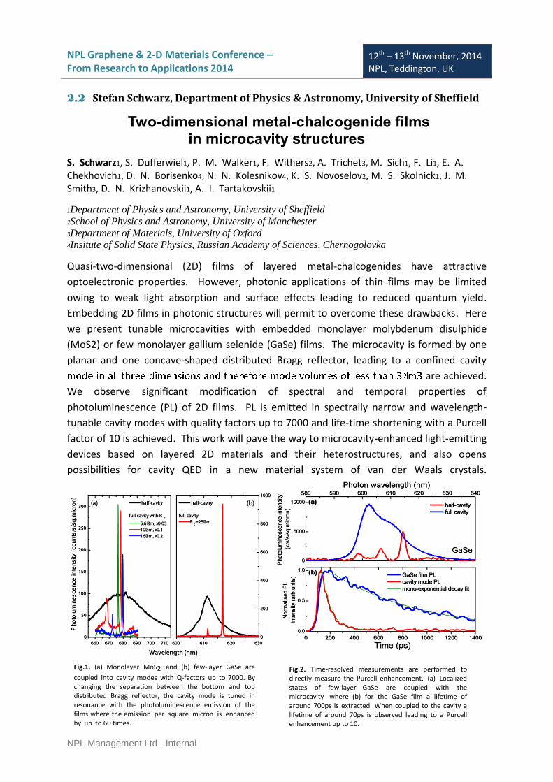
Fig.1. (a) Monolayer MoS2 and (b) few-layer GaSe are
coupled into cavity modes with Q-factors up to 7000. By changing the separation between the bottom and top distributed Bragg reflector, the cavity mode is tuned in resonance with the photoluminescence emission of the films where the emission per square micron is enhanced by up to 60 times.
Fig.2. Time-resolved measurements are
performed to directly measure the Purcell
enhancement. (a) Localized states of
few-layer GaSe are coupled with the
microcavity where (b) for the GaSe film
Fig.2. Time-resolved measurements are performed to directly measure the Purcell enhancement. (a) Localized states of few-layer GaSe are coupled with the microcavity where (b) for the GaSe film a lifetime of around 700ps is extracted. When coupled to the cavity a lifetime of around 70ps is observed leading to a Purcell enhancement up to 10.
NPL Graphene & 2-D Materials Conference – From Research to Applications 2014
12th – 13th November, 2014 NPL, Teddington, UK
NPL Management Ltd - Internal
2.3 Nicholas D. Kay, Physics Department, Lancaster University
Subsurface imaging of 2D materials on the nanoscale
Franco Dinelli1, Pasqualantonio Pingue3, S. Meucci3, Nicholas D. Kay1, Benjamin J. Robinson1, Vladimir I. Falko1 and Oleg V. Kolosov1
1 Physics Department, Lancaster University, Lancaster, LA1 4YB, UK, 2 CNR, Istituto Nazionale di Ottica (INO), via Moruzzi 1, 56124 Pisa, Italy 3 Laboratorio NEST - Scuola Normale Superiore, and Istituto Nanoscienze - CNR, Piazza San Silvestro
12, I-56127 Pisa, Italy
Scanning probe Microscopy (SPM) represents a powerful tool that in the past thirty years
has allowed one to investigate material surfaces in unprecedented ways at the nanoscale
level. However it has shown very little power of penetration, whereas several
nanotechnological applications would require it. Indeed subsurface imaging has been
achieved in just a few cases, namely when subsurface objects influence the surface
electronic states or the thermal properties. Ultrasonic Force Microscopy (UFM). a variation
of the Atomic Force Microscope (AFM) developed for the elastic investigation of stiff
materials, has also proven capable of sensing subsurface features.
In this paper we report on some investigations performed on 2D materials such as Graphene
and MoS2. In a first instance thick flakes have been placed on structured polymeric
substrates in order to prove that UFM can non-destructively distinguish suspended and
supported areas. UFM can also individuate defects due to delamination or buckling of
adjacent layers under stress. Consequently, interfaces between Graphene layers and
various substrates can be easily characterised. The reason of such a power of investigation
is that UFM is very sensitive to the indentation induced by the mechanical interaction
between tip and sample. Any tiny variation in the local indentation, either caused by
flexural bending of the suspended areas or by Young's modulus changes in the volume
perturbed by the applied elastic field, can be detected and imaged. Finally we shall report
on the mechanical characterization of fully suspended Graphene layers in the MHz range.
NPL Graphene & 2-D Materials Conference – From Research to Applications 2014
12th – 13th November, 2014 NPL, Teddington, UK
NPL Management Ltd - Internal
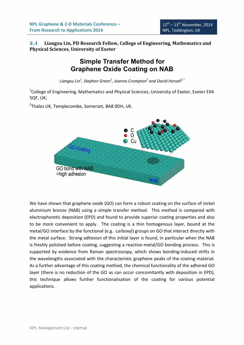
2.4 Liangxu Lin, PD Research Fellow, College of Engineering, Mathematics and Physical Sciences, University of Exeter
Simple Transfer Method for Graphene Oxide Coating on NAB
Liangxu Lin1, Stephen Green1, Joanna Crompton2 and David Horsell1,*
1College of Engineering, Mathematics and Physical Sciences, University of Exeter, Exeter EX4 5QF, UK;
2Thales UK, Templecombe, Somerset, BA8 0DH, UK.
We have shown that graphene oxide (GO) can form a robust coating on the surface of nickel
aluminium bronze (NAB) using a simple transfer method. This method is compared with
electrophoretic deposition (EPD) and found to provide superior coating properties and also
to be more convenient to apply. The coating is a thin homogenous layer, bound at the
metal/GO interface by the functional (e.g. carboxyl) groups on GO that interact directly with
the metal surface. Strong adhesion of this initial layer is found, in particular when the NAB
is freshly polished before coating, suggesting a reactive-metal/GO bonding process. This is
supported by evidence from Raman spectroscopy, which shows bonding-induced shifts in
the wavelengths associated with the characteristic graphene peaks of the coating material.
As a further advantage of this coating method, the chemical functionality of the adhered GO
layer (there is no reduction of the GO as can occur concomitantly with deposition in EPD),
this technique allows further functionalisation of the coating for various potential
applications.
NPL Graphene & 2-D Materials Conference – From Research to Applications 2014
12th – 13th November, 2014 NPL, Teddington, UK
NPL Management Ltd - Internal
Invited Speaker 2.5 Dr. Amaia Zurutuza, Scientific Director, Graphenea S.A., San Sebastian, Spain
Graphene: from Synthesis to Applications
Researchers envision many different applications for graphene although so far industrial
applications have been elusive. The term graphene covers a family of different materials and
depending on the type of graphene, the corresponding properties and potential applications
will vary. The graphene powder/flake form could meet large volume/weight requirements
and can be obtained from graphite. While the large area graphene films can be obtained
using silicon carbide sublimation and chemical vapor deposition (CVD) methods. The various
synthesis methods to produce graphene will be described as well as some potential
applications that we are currently investigating such as the use of graphene films in
extremely sensitive biosensors,1 as transparent electrodes in OLEDs,2,3 in the control of
plasmons with metal antennas,4 and for the formation of nanopores for future DNA
sequencing.5 In addition, I will try to shed some light on the time to market of these
applications and provide some views on the future commercialisation of graphene.6,7
[1] O. Zagorodko, J. Spadavecchia, A. Yanguas Serrano, I. Larroulet, A. Pesquera, A. Zurutuza, R. Boukherroub and S. Szunerits, Anal. Chem. DOI: 10.1021/ac502705n. [2] J. Meyer, P.R. Kidambi, B.C. Bayer, C. Weijtens, A. Kuhn, A. Centeno, A. Pesquera, A. Zurutuza, J. Robertson and S. Hofmann, Sci. Rep., 4 (2014) 5380. [3] L. D’Arsié, S. Esconjauregui, R. Weatherup, Y. Guo, S. Bhardwaj, A. Centeno, A. Zurutuza, C. Cepek and J. Robertson, Appl. Phys. Lett., 105 (2014) 103103. [4] P. Alonso-González, A.Y. Nikitin, F. Golmar, A. Centeno, A. Pesquera, S. Vélez, J. Chen, G. Navickaite, F. Koppens, A. Zurutuza, F. Casanova, L. E. Hueso and R. Hillenbrand, Science, 344 (2014) 6190. [5] W.L. Wang, E.J.G. Santos, B. Jiang, E.D. Cubuk C. Ophus, A. Centeno, A. Pesquera, A. Zurutuza, J. Ciston, R. Westervelt, and E. Kaxiras, Nano Lett., 14 (2013) 450. [6] H. Alcalde, J. de la Fuente, B. Kamp and A. Zurutuza, Proc. of the IEEE, 101 (2013) 1793. [7] A. Zurutuza and C. Marinelli, Nat. Nanotech., 9 (2014) 730.

NPL Graphene & 2-D Materials Conference – From Research to Applications 2014
12th – 13th November, 2014 NPL, Teddington, UK
NPL Management Ltd - Internal
Section 3 – Metrology & Standardisation
3.1 Dr. Vishal Panchal, NPL
Standardised electrical measurements of localised effects in graphene nanodevices
Localised variations in the electronic properties of 2D materials, such as layer
inhomogeneity and edge effects, can play a major role in governing the performance of
nanoscale devices. However, the electronic properties of these localised effects are
impossible to measure using standard transport techniques alone. We have overcome this
limitation by developing a standardised technique, which uses frequency-modulated Kelvin
probe force microscopy (FM-KPFM) and standard transport, to study localised effects in
nanodevices.
We have studied effects of thickness variations and edges in side-gated Hall bar nanodevices
made of epitaxial graphene. First, we have shown that FM-KPFM can be used to perform
calibrated work function measurements on mono- (Φ1LG ~4.55±0.02 eV) and bi-layer
graphene (Φ2LG ~4.44±0.02 eV) in ambient air [1]. We then demonstrate that
lithographically defined edges of the graphene channel exhibit hole conduction within the
narrow band of 60–125 nm width, whereas the bulk of the device is electron doped [2]. The
effect is the most pronounced when the influence of atmospheric contamination is minimal.
We also show that the electronic properties at the edges can be precisely tuned from hole
to electron conduction by using moderate strength electrical fields created by side-gates.
However, the central part of the channel remains relatively unaffected by the side-gates and
retains the bulk properties of graphene.
This standardised measurement technique could be used to quantitatively study any form of
local variations in the electronic properties of graphene and other 2D material devices.
[1] V. Panchal et al., Scientific Reports, 3, 2597 (2013) [2] V. Panchal et al., Scientific Reports, 4, 5881 (2014)
NPL Graphene & 2-D Materials Conference – From Research to Applications 2014
12th – 13th November, 2014 NPL, Teddington, UK
NPL Management Ltd - Internal
3.2 Cay-Christian Kalmbach, Physikalisch-Technische Bundesanstalt (PTB), Braunschweig , Germany
Towards a Graphene-based Quantum Impedance Standard C.-C. Kalmbach1, J. Schurr1, F. J. Ahlers1, A. Müller1, S. Novikov2, N. Lebedeva2, and A. Satrapinski3
1Physikalisch-Technische Bundesanstalt, Bundesallee 100, D-38116 Braunschweig, Germany 2Department of Micro- and Nanosciences, Aalto University, Micronova, Tietotie 3, 02150 Espoo, Finland 3MIKES, Tekniikantie 1, P.O.Box, 02151 Espoo, Finland
Ac measurements of the quantum Hall resistance in epitaxial graphene have been
performed in order to assess its suitability as a quantum standard of impedance. The
quantum Hall plateaus measured with alternating current on graphene Hall bar devices are
flat within one part in 107. Unlike in non-double-shielded GaAs devices, the graphene
device exhibits no frequency dependent curvature within the quantum Hall plateau at filling
factor ν = 2, thus magnetic-flux-dependent capacitive ac losses of the graphene device are
less critical. The observed frequency dependence of about -8·10-8/kHz is comparable in
absolute value to the positive frequency dependence of plain GaAs devices. We attribute
the negative sign of the frequency dependence of our graphene device to stray capacitances
which we believe can be minimized by a careful design of the graphene device. The
different origins of positive and negative contributions to the frequency dependence are
discussed. These results encourage further efforts to realize a graphene-based quantum
impedance standard even without the need for complex shielding methods. Further
improvements thus may lead to a simpler and more user-friendly quantum standard for
both resistance and impedance.
NPL Graphene & 2-D Materials Conference – From Research to Applications 2014
12th – 13th November, 2014 NPL, Teddington, UK
NPL Management Ltd - Internal
3.3 Wilfred Poirier, Laboratoire national de métrologie et d'essais (LNE), Paris, France
Quantum Hall resistance standard based on graphene grown by CVD on SiC
F. Lafont1, R. Ribeiro-Palau1, D. Kazazis2, A. Michon3, B. Jouault4, O. Couturaud4, C. Consejo4,
M. Zielinski5, Th. Chassagne5, M. Portail3, B. Jouault4, F. Schopfer1, and W. Poirier1
1Laboratoire National de Métrologie et d’Essais, Trappes, 78190, France 2Laboratoire de Photonique et Nanostructures, CNRS, Marcoussis, 91460, FRANCE 3CRHEA, CNRS, Valbonne, 06560, FRANCE 4Laboratoire Charles Coulomb, Université de Montpellier 2, CNRS, Montpellier, 34095, FRANCE 5NOVASiC, Le Bourget du Lac, 73370, FRANCE
We will present recent quantum Hall resistance measurements in large (100 × 420 µm2) Hall
bars based on graphene grown by chemical vapor deposition of propane under hydrogen on
the Si-face of SiC substrates, a scalable growth technique recently developed [1]. Owing to
low electron density of 3.2×1011 cm-2 and mobility of 3 000 cm2V-1s-1, at T = 1.3 K, the 10-
large range of magnetic fields from B = 10 T and up to 19 T (max field available in the lab).
The longitudinal resistance Rxx per square is measured below
substitute to GaAs–ones as a primary resistance standard, operating with the same
precision and in similar cryomagnetic conditions. The mean value of the Hall resistances
measured on the plateau amounting to (-0.2 +/- 4) ×10-10 also gives an additional proof of
the QHE universality. We have investigated the dissipation using the accurate metrological
tools based on SQUID technology. The temperature and current dependences of the
longitudinal conductivity show that the dominant mechanism of dissipation is based on
variable range hopping with soft coulomb gap and then allow a determination of the
localization length of states at Fermi energy. It is observed that the perfect quantization of
the Hall resistance over a large magnetic field range is accompanied by the localization
length locked to the magnetic length. This behaviour is correlated with the structural
properties of the graphene samples.
The presented work [2] confirms the graphene promises for the resistance metrology
application. It also emphasizes the quality of the graphene produced by the CVD on SiC and
its interest for electronic applications as demanding as the resistance metrology.
[1] A. Michon et al., Appl.Phys. Lett. 97, 171909 (2010). [2] F. Lafont et al. arXiv: 1407.3615 (2014).
NPL Graphene & 2-D Materials Conference – From Research to Applications 2014
12th – 13th November, 2014 NPL, Teddington, UK
NPL Management Ltd - Internal
Section 4 – Flexible Electronics & Sensors
Invited Speaker 4.1 Dr. Liam Britnell, Research Manager, BGT Materials Ltd., University of Manchester
Graphene materials for flexible electronics
Established in 2013, BGT Materials has the capability to produce a range of graphene
materials. The company holds proprietary processes to produce high quality CVD
graphene, graphene oxide and graphene conductive inks. I will discuss our experience in
using these materials in product development and applications; mainly focusing on CVD
graphene for flexible electronics.
It is well known that industry is searching for a replacement for ITO in touch panels but
market forecasts do not predict any competing technology to take a significant market
share. We believe that through innovative product design we can utilize the properties of
graphene to create new applications. I will discuss both where we feel graphene can
succeed and where it cannot, and the evolution and standards that need to be adopted
within the industry in order for the potential of graphene to be realised.
NPL Graphene & 2-D Materials Conference – From Research to Applications 2014
12th – 13th November, 2014 NPL, Teddington, UK
NPL Management Ltd - Internal
Invited Speaker 4.2 D. Kurt Gaskill, Research Physicist, Naval Research Laboratory, Washington DC, USA
Recent Advancements in Avoiding Dirt: Clean Epitaxial Surfaces for Device Applications
D.K.Gaskill1, A.Nath2, A. D. Koehler1, M. Currie1, M.J. Tadjer3, V. D.Wheeler1, Z. R. Robinson3, A.D.Boyd3, R. L. Myers-Ward1, C. R. Eddy Jr1, and M.V. Rao2
1U.S. Naval Research Laboratory, 4555 Overlook Ave., SW, Washington, DC 20375, USA 2George Mason University, 4400 University Dr. Fairfax, Virginia, VA 22030, USA 3American Society of Engineering Education Postdoctoral Fellow, 1818 N St NW, Washington, DC 20036, in-residence at U.S. Naval Research Laboratory
Graphene-metal interaction continues to be an interesting problem for the graphene
community. Controlled tailoring of the graphene-metal contact resistance is essential to
exploit graphene’s extraordinary electronic, optical, thermal and mechanical properties.
Intrinsic effects such as the density of states (DOS) bottleneck near the Dirac point, carrier
reflection at the contact metalgraphene interface due to momentum mismatch or due to
formation of a p-n junction increase contact resistance. Extrinsically, surface contamination
introduced by polymers, solvents, chemicals and other adsorbates such as water during
standard semiconductor processing increase contact resistance through increased
scattering. To understand the intrinsic limitations of graphene-metal interaction, we report
a femto-second laser assisted lithography technique which enables us to characterize
pristine graphene-metal contact resistance. Moreover, a sacrificial polymer-assisted
procedure that produces a clean graphene surface following device fabrication by a
standard lithography process is also discussed. The Landauer-Buttiker model is used to
explain carrier transport at the graphene-metal interface. We show that the graphene-
metal contact resistance is primarily limited by graphene-metal vertical carrier transmission
and edgestate conduction is necessary to obtain contact resistance near the quantum
contact resistance limit.
NPL Graphene & 2-D Materials Conference – From Research to Applications 2014
12th – 13th November, 2014 NPL, Teddington, UK
NPL Management Ltd - Internal
4.3 Dr. Cristina Giusca, NPL
The effect of ambient humidity on the electronic properties of epitaxial graphene
C.E. Giusca1, V. Panchal, M. Munz, V.D. Wheeler2, L.O. Nyakiti3, R.L. Myers-Ward2, C.R. Eddy, Jr.2,
D. K.Gaskill2, O. Kazakova1
1National Physical Laboratory, Hampton Road, Teddington, TW11 0LW, United Kingdom 2U.S. Naval Research Laboratory, Washington, DC 20375, United States of America 3Texas A&M University, Galveston, TX 77553, United States of America
An important concern regarding graphene-based devices that are normally operated in
ambient environment is that water and gas molecules reacting with graphene have an
influence on devices performance and reliability. Significant effort has been dedicated to
both theoretical and experimental investigation of water on graphitic surfaces. However, in
spite of these intense activities, a complete understanding of the water-graphene
interaction is still lacking.
In the current work, we employ scanning Kelvin probe microscopy (SKPM) to study the
effect that water has on the electronic properties of epitaxial graphene, directly correlated
with the local structural information. We study the influence of relative humidity (RH=0-
70%) changes on the surface potential of single-, bi- and tri-layer epitaxial graphene (1LG,
2LG and 3LG, respectively) and demonstrate the reversible process of water vapour
adsorption and desorption on the various graphene domains.
We also monitor the effect that the change in environment, from ambient to vacuum and to
nitrogen, has on the electronic properties of epitaxial graphene. Based on the surface
potential data recorded by SKPM, a lower carrier (electron) concentration in 2LG relative to
1LG, ne(2LG)<ne(1LG), is found in vacuum compared to ambient, where 2LG shows a higher
carrier concentration than 1LG, ne(2LG)>ne(1LG). The observed effect is explained in terms
of an increase of the electron concentration in both 1LG and 2LG on ambient-vacuum
transition due to desorption of environmental p-dopants. Exposing the sample to increasing
humidity levels, ranging between 10% and 70%, causes a gradual decrease in absolute value
of the contact potential difference determined by SKPM, consistent with a higher carrier
concentration in 2LG compared to 1LG and with the addition of p-dopants.
The results demonstrate the importance of surface studies of graphene in ambient, as well
as at elevated humidity conditions, in order to fully understand the underlying physical
phenomena and exploit possibilities for design and fabrication of graphene devices and
sensing platforms.
NPL Graphene & 2-D Materials Conference – From Research to Applications 2014
12th – 13th November, 2014 NPL, Teddington, UK
NPL Management Ltd - Internal
Invited Speaker 4.4 Dr. Richard White, Principal Engineer, Sensor Systems, Nokia Technologies., Cambridge, UK
Exploiting 2D materials for printed sensor applications
The global sensor market is set to grow from $79.5bn in 2014 to $116bn in 2019[1] largely
due to the emergence of the Internet of Things. A sensor is more than the sensitive element
itself and includes other functions such as signal processing, memory and communications.
Graphene and graphene-related materials can play a critical role in many facets of the
‘sensor’ and since many of the outstanding properties of 2D materials are intrinsic to the
materials themselves this presents the attractive prospect of using low-cost and highly-
scalable methods for their manufacture. This talk will present some of Nokia’s recent work
in printed flexible electronics and highlights two promising applications of 2D materials that
have been studied at Nokia. First, a graphene oxide humidity sensor that has demonstrated
unprecedented response speeds down to 30 ms[2] and second, a MoS2 memristor that
possesses a tunable electrical resistance range of 102 to 108 Ω with programming voltages
less than 0.2 V[3].
1. Electronics.ca Research Network; Global markets & technologies for sensors; May 2013
2. Borini, S. et al, Ultrafast Graphene Oxide Humidity Sensor, ACS Nano 7(12), 2013
3. Bessonov, A. et al, Layered memristive and memcapacitive switches for printable
electronics, Nature Materials (accepted) 2014
NPL Graphene & 2-D Materials Conference – From Research to Applications 2014
12th – 13th November, 2014 NPL, Teddington, UK
NPL Management Ltd - Internal
Day 2 – Thursday, November 13th
Section 5 – Graphene Stakeholders Association
Invited Speaker 5.1 Stephen Waite, Co-Founder and Co-Executive Director Graphene Stakeholders Association
The Graphene Stakeholders Association (GSA) was formed in the spring of 2013 to foster the responsible development of graphene and other 2-D materials and facilitate the process of accelerated innovation with graphene and other 2-D materials within the emerging ecosystem. Shortly following the launch, the GSA began collaborating with the NPL who became a lifetime member of the association. The collaboration has been well received in the graphene and 2-D materials community and continues to grow with the launch of the GSA’s Center of Excellence (CoE) initiative in the fall of 2014. This talk will highlight the fruits of the collaboration of the GSA and NPL, discuss the new CoE initiative and its role in helping to fulfill the GSA’s mission, and emphasize the growing opportunities for graphene and 2-D materials-enabled innovation associated with emerging additive manufacturing and 3-D printing technology.
5.2 Ray Gibbs, Haydale Limited, Ammanford, UK
Graphene: Current trends, Opportunities & Solving the Commercialisation Issue
NPL Graphene & 2-D Materials Conference – From Research to Applications 2014
12th – 13th November, 2014 NPL, Teddington, UK
NPL Management Ltd - Internal
5.3 Sarbajit Banerjee, Ph.D., Professor of Chemistry, Department of Chemistry, Texas A&M University, College Station, USA
How Graphene Talks to Other Stuff: Fundamental Explorations of Graphene Interfaces and the Design of
Graphene Nanocomposites: Given the entirely surficial geometric structure of graphene, the extent of manifestation of
true Dirac physics in this material is substantially modulated by perturbations of the
electronic structure as a result of interactions with charged impurities, coupling to the
underlying substrate, orbitalhybridization with deposited contacts, and buckling/corrugation
of graphene sheets.
Fundamental studies of perturbations of graphene electronic structure are thus imperative
for the rational design of graphene interfaces and for incorporation of graphene within
polymeric and metal matrix composites. In this talk, I will focus on the results of our
combined X-ray absorption spectroscopy, Raman microprobe analysis, and density
functional theory studies of graphene/metal and graphene/dielectric interfaces.
Depending on the nature of the transition metal and the proximity of the graphene surface,
physisorption or covalent chemical bonding is observed. Studies of the hybridization of
single-crystalline metal surfaces with graphene suggest clear facet selectivity. We further
evidence the potential for anisotropically functionalizing only one surface of planar
graphene. For dielectric interfaces, charge transfer is observed without formation of
carbidic bonds. I will further discuss the design of graphene— polyetherimide
nanocomposites based on engineered graphene interfaces that endow remarkable
corrosion protection to low alloy steel upon application as thin films and conclude with the
development of graphene—epoxy formulations for coating and moldable plastic
applications based on the use of graphene oxide as a curing agent.
1) Brian J. Schultz, Christopher J. Patridge, Vincent Lee, Cherno Jaye, Patrick D. Lysaght, Casey Smith, Joel Barnett, Daniel A. Fischer, David Prendergast,* Sarbajit Banerjee,* Imaging Local Electronic Corrugations and Doped Regions in Graphene, Nature Commun., 2011, 2, 372/1-372/8. 2) Robert V. Dennis, Lasantha T. Viyannalage, Anil V. Gaikwad, Tapan K. Rout, and Sarbajit Banerjee,* Graphene Nanocomposite Coatings for Protecting Low-Alloy Steels from Corrosion. Am. Ceram. Soc. Bulletin 2013. 92, 18-24 3) Brian J. Schultz, Robert V. Dennis, Vincent Lee, and Sarbajit Banerjee,* An Electronic Structure Perspective of Graphene Interfaces, Nanoscale 2014, 6, 3444-3466.
NPL Graphene & 2-D Materials Conference – From Research to Applications 2014
12th – 13th November, 2014 NPL, Teddington, UK
NPL Management Ltd - Internal
5.4 Dr. Andrew Pollard, NPL
Metrology for Graphene: Measurement and Standardisation as an Industry Enabler
As the UK’s leading National Measurement Institute (NMI), the National Physical Laboratory
(NPL) is uniquely positioned to enable the global emerging graphene industry through the
application of metrology in this area, bridging the gap between academia and industry.
With measurement capability and expertise in a wide range of scientific areas, the combined
and complementary approach of varied characterisation methods for structural, chemical,
electrical and other properties, allows the real-world challenges of commercialising
graphene and other 2-D materials to be addressed.
Examples of metrology challenges that have been overcome through cross-disciplinary
research, newly developed measurement techniques and collaboration with both academia
and industry will be discussed, for specific consumer application areas. In addition, the role
of international standardisation in this area will also be described and the current work
ongoing in both ISO and IEC will be outlined.
NPL Graphene & 2-D Materials Conference – From Research to Applications 2014
12th – 13th November, 2014 NPL, Teddington, UK
NPL Management Ltd - Internal
Section 6 – Composites
6.1 Francesco Bisio, Ph.D., Researcher, CNR-SPIN, Genova, Italy
Plasmonic response of composite graphene-Au nanopatterned systems
We investigated the optical response of a hybrid graphene/plasmonic device consisting of a
2-dimensional gold nanoparticles (NPs) array combined with a single-layer-graphene foil.
The Au NPs were fabricated on a self-organized nanopatterned CaF2(110) surface, and
exhibited a well-defined localized surface plasmon (LSP) at 580 nm.
Large foils of mostly-single-layer graphene were fabricated by chemical vapour deposition
on Cu foils, then transferred onto the Au nanopatterns in aqueous solution. The unique
electronic properties of graphene coupled with metallic nanostructures are expected to lead
to significant perturbation of the local distribution of electromagnetic field intensity, hence
the plasmonic response 1,2.
The system demonstrated a remarkable LSP-resonance red shift as the single graphene layer
is transferred on the gold nanoparticles, due to the successful achievement of a modified
near-field electromagnetic coupling between plasmon-resonance mode of adjacent
nanoparticles via the graphene film. The Au NPs remain intact, in shape and spatial
arrangement, following the graphene deposition, proving the realization of a hybrid
plasmonic/graphene medium.
1. Wang, P.; Zhang, W.; Liang, O.; Pantoja, M.; Katzer, J.; Schroeder, T.; Xie, Y.-H, “Giant optical response from graphene- plasmonic system” ACS Nano 6, 6244−6249 (2012).
2. Jing Niu; Young Jun Shin; Jaesung Son; Youngbin Lee; Jong-Hyun Ahn; and Hyunsoo Yang, “Shifting of surface Plasmon resonance due to electromagnetic coupling between graphene and Au nanoparticles “ Optical Express 20, 19690 (2012).
NPL Graphene & 2-D Materials Conference – From Research to Applications 2014
12th – 13th November, 2014 NPL, Teddington, UK
NPL Management Ltd - Internal
6.2 Dr. Toby Sainsbury, NPL
2-D Nanomaterials: Emerging Material Platforms
2-D Nanosheet materials have emerged in recent years as a class of materials which promise
step changes in bulk material properties when configured in a composite fashion. The
intrinsic properties of 2-D nanomaterials encompass high electrical conductivity, insulating
and semi-conducting properties, high thermal conductivity, high mechanical strength, gas
diffusion barriers, high chemical stability and radiation shielding. 2-D nanomaterials such as
graphene, h-BN or MoS2 offer such attractive properties which have been validated through
focussed proof of concept studies. There therefore remains significant motivation to
establish means by which such properties are translated to bulk scale materials or mass
production scales. It is also evident that to enable the utilisation of 2-D nanomaterials over
a range of envisaged technological applications that efforts must be focussed on the
interfacial aspects of 2-D nanomaterial integration. It is evident that device electronics will
be dominated by contact resistance issues, whereas phonon transport in thermal
management systems will rely on optimization of interfacial surface area and material
coupling. The dispersion and optimized integration of 2-D nanomaterials will be central to
the utilization of these materials within nanocomposite applications for mechanical, barrier
and radiation shielding applications. It is clear to enable initial dispersion and integration of
these materials that chemical strategies for surface functionalization and bonding to
substrates and material matrices will enable the optimized material utilization.
Here we report approaches to engineer the surface chemical composition of graphene and
h-BN by the use of reactive radical surface functionalization and the direct attachment of
polymer chains to graphene oxide and h-BN-oxide nanosheets. Solution phase exfoliation of
graphene has been performed in order to facilitate optimal surface area for covalent
chemical functionalization. Reactive carbene radical species are generated in solution which
form cyclopropyl adducts with graphene. the covalent functionalization has been
characterized using FTIR, UV-Vis, Raman, ToF-SIMS, XRD, XPS, TGA, EDX, SEM and TEM. By
these means, graphene and h-BN may be chemically functionalized in order to manipulate
the intrinsic optoelectronic properties and to control the interface with polymer systems for
mechanical reinforcement.
NPL Graphene & 2-D Materials Conference – From Research to Applications 2014
12th – 13th November, 2014 NPL, Teddington, UK
NPL Management Ltd - Internal
Section 7 – High Frequency Electronics
Invited Speaker 7.1 Prof. Dr. Thomas Seyller, Technische Universität Chemnitz, Institut für Physik – Technische Physik, Chemnitz, Germany
Contact Metals on Graphene: A Photoemission Study
R. J. Koch1, A. H. Hsu2, M. Ong3, M. Hofmann2, E. Reed3, M. Dresselhaus2, J. Kong2, T. Palacios2, and Th. Seyller1
1) Institut für Physik, Technische Universität Chemnitz, 09126 Chemnitz, Germany, 2) Department of Electrical Engineering and Computer Sciences, Massachusetts Institute of Technology, Cambridge, Massachusetts 02139, USA, 3) Department of Materials Science and Engineering, Stanford University, Stanford, CA 94305, USA
The outstanding properties of graphene (high charge carrier mobility, exceptional
mechanical strength, chemical resistance, etc.) suggest various applications in the areas of,
e.g., high frequency electronic devices, MEMS, optoelectronics, plasmonics, sensors, or
photovoltaics. In almost every application, electrical contacts are necessary between the
graphene and the surrounding circuitry. This is simply done by depositing a suitable metal
on top of graphene. However, the electrical properties of the contact depend on the chosen
metal, as it determines work function differences as well as chemical reactions that might
occur at the interface. On the other hand, the contact properties have great influence on
the device performance. Therefore, a detailed understanding of metal/graphene interfaces
is mandatory in order to gain precise control over electrical contacts in devices.
Different metals or combinations of metals are employed. Among others, gold (Au) is used
in conjunction with titanium (Ti) or chromium (Cr), which acts as a bonding agent.
Palladium (Pd) or nickel (Ni), deposited directly onto graphene, has also been used in
contacts. In the present work we employ photoelectron spectroscopy to study the interface
between these metals and epitaxial graphene grown on silicon carbide. Whereas core level
photoelectron spectroscopy (XPS) is used to analyze the chemical bonding between the
metals and the graphene substrate, angle-resolved valence band photo electron
spectroscopy (ARPES) is employed to study changes in the electronic structure of the
graphene. Experimentally this is done by acquiring spectra continuously during metal
deposition using high-brilliance synchrotron radiation. The experiment thus allows us to
study the evolution of the interface with increasing metal coverage. Moreover, the
comparison of high resolution spectra taken before and after metal deposition allows us to
observe even subtle changes in the bonding configuration of graphene and the deposited
metal. Note, that the results are not the same as that for graphene grown on these metals
due to markedly different conditions.

NPL Graphene & 2-D Materials Conference – From Research to Applications 2014
12th – 13th November, 2014 NPL, Teddington, UK
NPL Management Ltd - Internal
7.2 Myung-Ho Bae, Principal Research Scientist, Center for Quantum Measurement Science, Korea Research Institute of Standards and Science
Energy Dissipation in Graphene Nanodevices
Energy dissipation in nanoscale electronics has become an important subject in modern
electronic industry and energy conversion system. From this perspective, graphene with
very high mobility and thermal conductivity, which are about ten times higher than silicon, is
a very attractive nano-material to study energy dissipation in nano-electronics. My talk will
present studies for the gate-controllable Joule heating and Peltier cooling in graphene
devices. I will also talk about the phonon transport through graphene nanoribbons.
NPL Graphene & 2-D Materials Conference – From Research to Applications 2014
12th – 13th November, 2014 NPL, Teddington, UK
NPL Management Ltd - Internal
7.3 Nathan Mahlmeister, University of Exeter
Mid-Infrared Thermal Emission from Large Area Graphene
In recent years thermal emission from graphene has been used as a means to probe its
electronic and thermal properties1. In small area graphene transistors the cause of the
thermal emission is Joule heating in nature2 and a hot spot arises corresponding to the
position of the charge neutrality point (CNP) along the conduction channel2. The position
of the CNP can be moved by altering the number of charge carries via the back gate.
Recently, we have investigated3 the spatial variation of thermal emission from large area
CVD graphene devices. Using a 1D finite element model, which accounts for Joule heating
and electrostatic effects, it is found that the non-uniform thermal emission is governed by
the charge distribution in the graphene and that maximum Joule heating occurs at the point
of minimum charge density. The observed thermal emission from these large area devices
is therefore qualitatively the same as seen from much smaller exfoliated devices.
However, not only can the thermal emission be used to probe the properties of graphene,
its low thermal mass and robustness also means that graphene is promising for use as an
incandescent infrared emitter. We have measured the spectra from both large area mono
and multilayer graphene devices4 on SiO2/Si and show that the emission is broadly that of a
grey body emitter. For the drive currents used, which could be sustained in the devices for
more than one hundred hours, the emission peaked at 4μm and covered the characteristic
absorption of many important gases. A measurable thermal emission was obtained even
when the drive current was modulated at frequencies up to 100 kHz. Further work is now
underway to investigate methods of increasing the potential modulation speed and of
increasing the emissivity of the emitting area.
1 M. Bae, Z. Ong, D. Estrada, and E. Pop, Nano Lett. 10, 4787 (2010).
2 M. Freitag, M. Steiner, Y. Martin, V. Perebeinos, Z. Chen, J. Tsang, and P. Avouris, Nano lett. 9, 1883 (2009).
3 I. J. Luxmoore, C. Adlem, T. Poole, L. M. Lawton, N. H. Mahlmeister, and G. R. Nash, Appl. Phys. Lett. 103, 131906 (2013).
4 L. M. Lawton, N. H. Mahlmeister, I. J. Luxmoore and G. R. Nash, “High frequency mid-infrared thermal emission from large area graphene” Under Review (2014).
NPL Graphene & 2-D Materials Conference – From Research to Applications 2014
12th – 13th November, 2014 NPL, Teddington, UK
NPL Management Ltd - Internal
7.4 Dr. Adam Gilbertson, Research Associate, Department of Physics, Imperial College London
Ultrafast hot carrier dynamics in a hybrid graphene-metal plasmonic nanostructure
Adam Gilbertson, Tyler Roschuk, Themis Sidiropoulos, Viktoryia Shautsova, Vincenzo Gianinni, Yiguo Chen, Stefan Maier, Rupert Oulton, Lesley Cohen
Graphene exhibits ultrafast broadband absorption that has attracted considerable interest
for optoelectronic applications. A major hurdle for real applications is the low optical
absorption (2.3%) of graphene, limited by its atomic thickness. A promising approach is to
integrate graphene with metallic nanoparticles that focus light into nanoscopic volumes,
promoting strong absorption.1 This hybrid system is particularly interesting from a
fundamental view point but has been little explored. The electronic and thermal coupling of
a resonantly excited plasmonic nanoparticle (NP) array with a graphene 2D electron gas in
intimate contact results in perturbations to the hot carrier population via non-equilibrium
carrier heating, charge transfer or the near-field electric field enhancement at the NP
surface and can be studied through the transient differential reflectivity. We perform two-
colour pump-probe measurements using linearly polarised 200fs pulses to probe the photo-
excited hot-carrier dynamics of the graphene overlayer under resonant excitation of the NP.
We demonstrate that the presence of the NP results in significant modifications to the hot
carrier relaxation in the graphene including a pronounced ultrafast absorption anisotropy.
1. T. J. Echtermeyer, L. Britnell, P. K. Jasnos, A. Lombardo, R. V. Gorbachev, A. N.
Grigorenko, A. K. Geim, A. C. Ferrari, and K. S. Novoselov, Nature Communications 2, (2011).
NPL Graphene & 2-D Materials Conference – From Research to Applications 2014
12th – 13th November, 2014 NPL, Teddington, UK
NPL Management Ltd - Internal
Invited Speaker 7.5 Shu-Jen Han, Research Staff Member, IBM T.J. Watson Research Center, USA
Nanoelectronics Based on Graphene and Beyond
Graphene has attracted much interest as a future channel material in high-frequency
electronics because of its superior electrical properties. Recent development has been
shifted from the device level study to the circuit level demonstration. I will review and
discuss several key challenges for large-scale graphene device fabrication, including high
quality gate dielectric, large-area film transfer, and output current saturation. Furthermore,
fabrication of a graphene integrated circuit without significantly degrading transistor
performance has proven to be challenging, posing one of the major bottlenecks to compete
with existing technologies. I will review our effort of developing graphene IC in the past few
years, starting with a simple 1-stage mixer built on a SiC piece, toward the recent
demonstration of a high-performance three-stage graphene IC that fully preserves graphene
transistor quality post-IC fabrication. Beyond graphene, more suitable 2D materials with
energy bandgap for electronics applications are being aggressively investigated. I will
discuss some recent progress of transition metal dichalcogenides (TMDC) and black
phosphorus (BP) based transistors in my group. In addition, other applications such as
plasmonics and photodetectors using these novel 2D materials will be briefly discussed.
NPL Graphene & 2-D Materials Conference – From Research to Applications 2014
12th – 13th November, 2014 NPL, Teddington, UK
NPL Management Ltd - Internal
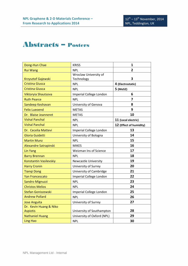
Abstracts – Posters
Dong-Hun Chae KRISS 1
Rui Wang NPL 2
Krzysztof Gajewski Wroclaw University of Technology 3
Cristina Giusca NPL 4 (Electrostatic)
Cristina Giusca NPL 5 (MoS2)
Viktoryia Shautsova Imperial College London 6
Ruth Pearce NPL 7
Sandeep Keshavan University of Genova 8
Felix Lueoend METAS 9
Dr. Blaise Jeanneret METAS 10
Vishal Panchal NPL 11 (Local electric)
Vishal Panchal NPL 12 (Effect of humidity)
Dr. Cecelia Mattevi Imperial College London 13
Gloria Guidetti University of Bologna 14
Martin Munz NPL 15
Alexandre Satrapinski MIKES 16
Lin Yang Weizman Ins of Science 17
Barry Brennan NPL 18
Konstantin Vasilevskiy Newcastle University 19
Harry Cronin University of Surrey 20
Tianqi Dong University of Cambridge 21
Yan Francescato Imperial College London 22
Sandro Mignuzzi NPL 23
Christos Melios NPL 24
Stefan Goniszewski Imperial College London 25
Andrew Pollard NPL 26
Jose Anguita University of Surrey 27 Dr. Kevin Huang & Niko Aspiotis University of Southampton 28
Nathaniel Huang University of Oxford (NPL) 29
Ling Hao NPL 30
NPL Graphene & 2-D Materials Conference – From Research to Applications 2014
12th – 13th November, 2014 NPL, Teddington, UK
NPL Management Ltd - Internal
1 Dong-Hun Chae, Korea Research Institute of Standards & Science
Experimental progress towards quantum Hall resistance metrology using CVD-graphene in KRISS Exfoliated graphene showed a potential for quantum resistance metrology under practically more favorable enviroments. However, such graphene flake is considered too small for the metrological purposes. There exist two scaleable graphene synthesized through graphitization of SiC and chemical vapor deposition growth. So far,the experimental enviroments have not been relaxed, compared to the conventional semiconductor heterostructure, with the epitaxial graphene on SiC even with intensive experimental efforts. In KRISS, we are checking the feasibility of CVD-graphene whose growth and transfer techniques have been recently improved very much. Here, we will show structural analysis of synthesized CVD-graphene using liquid crystal texture. We have also tried to realize graphene/boron-nitride heterosructure through CVD-synthesis and physical transfer method to reduce disorders from substrates. Preliminary results on magneto-transport of CVD-graphene Hall devices will be exhibited.
2 Rui Wang, NPL
Development of a non-contacting microwave method to investigate the electronic properties of graphene As graphene fabrication proceeds rapidly to industrial production levels there is an increasing need for fast, non-contacting characterisation methods able to deal with wafer scale material. We have demonstrated, and are continuing to develop, a microwave method for measuring conductivity and sheet resistance of graphene films. The method relies on the graphene film being brought within a few millimetres of a high quality factor(Q) dielectric microwave resonator. The presence of the graphene perturbs the standing wave properties of this resonator, leading to changes in Q and resonant frequency. Measurements of these changes allow the graphene electrical properties to be determined without the need to contact the film or pattern it. The measurements can be completed in a very short time. A substitution technique requiring only a blank substrate with no graphene on it, makes this an ideal quality control procedure since no calibration or modelling stages are required. We will report on further developments of this method aimed at measuring the mobility and carrier concentration of graphene samples and extending towards thermal property characterisation. We also discuss the relevance of the microwave method to other two dimensional materials.
NPL Graphene & 2-D Materials Conference – From Research to Applications 2014
12th – 13th November, 2014 NPL, Teddington, UK
NPL Management Ltd - Internal
3 Krzysztof Gajewski, Wroclaw University of Technology
Scanning probe microscopy study of the graphene nanoelectromechanical resonators Graphene, an sp2 bonded material made from carbon, makes a big interest of scientists since its discovery in 2004. It resulted in Nobel prize for A. Geim and K. Novoselov who was the first, who extract it from carbon. There were many investigations showing in graphene: integer quantum hall efect, its ambipolar properties or even relativistic behavior of its electrones. In our opinion it is still need to stydy graphene mechanical behavior, especially suspended over cavity.
In this work we would like to present results of our scanning probe microscopy (SPM) study of the graphene nanoelectromechanical resonators. Chemical vapor deposited graphene was transfered on the SiO2 array (containing square, circular and trench microstructures) with the use of PMMA transfer. In that way graphene formed membrane an doubly clamped beam nanostructures. Using scanning electron microscope, detection of freestanding graphene was performed. Involving SPM techniques we characterized influence of the wrinkles, grain domains, holes and other distortions on electrical properties of the graphene. Using Kelvin probe microscopy (KPFM) we observed that suspended graphene contact potential difference (CPD) differs for about 0.15 V in comparison to supportet graphene. It is the evidence of the strong influence of the substrate on the electrical properties of the graphene. We also observed much smaller influence of the wrinkles or even small holes on suspended graphene CPD in contrary to graphene lying on the substrate. Our KPFM investigations was extended by Conductive AFM measurements and also force spectroscopy.
NPL Graphene & 2-D Materials Conference – From Research to Applications 2014
12th – 13th November, 2014 NPL, Teddington, UK
NPL Management Ltd - Internal
4 Cristina Giusca, NPL
Electrostatic transparency of graphene oxide sheets
C.E. Giusca1, F. Perrozzi 2, L. Ottaviano2, E. Treossi3, V. Palermo3, O. Kazakova1
1National Physical Laboratory, Hampton Road, Teddington, TW11 0LW, United Kingdom 2Università dell’Aquila, & CNR-SPIN, Via Vetoio 10, 67100, L’Aquila, Italy 3CNR-ISOF- Laboratorio MIST.E-R, Via Gobetti 101, 40129 Bologna, Italy
Graphene’s disordered analogue, graphene oxide (GO), has originally been regarded as a precursor for cost-effective graphene production on a large scale but has become particularly attractive for practical applications based on its intrinsic chemical and electronic structure. For graphene layers, the interaction with the underlying substrate has been extensively studied and it was found to affect the conductivity, doping level or to significantly impact the noise level in graphene devices. At the same time, the influence of the supporting substrate on the electronic properties of GO has remained largely unexplored. In the current study, we probe the interaction of GO of varying reduction degrees with dielectric and metallic surfaces using scanning Kelvin probe microscopy (SKPM) and Raman spectroscopy, in order to assess the influence that the supporting substrate has on the electronic properties of graphene oxide and its reduced form. Lateral inhomogeneities in the distribution of subsurface charged impurities are found to affect the electronic properties of graphene oxide, giving rise to significant in-plane variations of the local electrostatic potential on reduced single layer graphene oxide supported on dielectric substrates. On the contrary, no such surface potential fluctuations are identified on as-produced graphene oxide sheets, or on graphene oxide layers deposited on a metallic substrate. Consistent with effective screening effects for thicker sheets, it is shown that reduced bi-layer graphene oxide on dielectric substrates is not electrostatically transparent to substrate trapped charge impurities. Raman spectroscopy studies highlight changes in the main Raman bands correlated with the reduction degree and point to an increase in crystalline order upon chemical reduction of GO. The current study provides a useful account of the limitations that GO device performance could face when attempting to tune the electronic structure of GO via chemical functionalization, highlighting the role of substrate-related disorder sources affecting the behaviour of nanoelectronic devices.
NPL Graphene & 2-D Materials Conference – From Research to Applications 2014
12th – 13th November, 2014 NPL, Teddington, UK
NPL Management Ltd - Internal
5 Cristina Giusca, NPL
Correlation of structural, nanomechanical and electrostatic properties of single and few-layers MoS2 C.E. Giusca1, Y. Teijeiro Gonzalez1, B.J. Robinson2, N.D. Kay2, O. Kolosov2, O. Kazakova1
1National Physical Laboratory, Hampton Road, Teddington, TW11 0LW, United Kingdom 2Department of Physics, Lancaster University, Lancaster, LA1 4YB United Kingdom Layered transition metal dichalcogenides have attracted significant attention due to their potential applications in electronic and optical devices. Molybdenum disulphide (MoS2) is one of the most stable layered materials of this class. In the bulk form this material has an indirect band gap of 1.3 eV, whereas monolayer MoS2 has a 1.8 eV direct band gap and prominent electro- and photoluminescent properties, making it a likely candidate for applications in photodetectors and light-emitting devices operating in the visible range. As electronic and optical properties of MoS2 are strongly thickness dependent, it is essential to precisely ascribe the measured parameters to individual layers. Raman spectroscopy has been widely used to determine the number of layers and examine the relevant changes in material properties, as the vibrational spectrum is sensitive to the sample thickness. On the other hand, surface potential of layered materials is also strongly dependent on the number of layers and the nanomechanical properties of those layers, arising from both intrinsic structure and defects and from the sample-substrate interface. Here, we perform a comprehensive study of mechanically exfoliated MoS2 flakes with the aim to precisely correlate their structural, nanomechanical and electrostatic properties on the nanoscale. The properties of the samples in dependence on the layer thickness and sample-substrate mechanical contact were investigated using Ultrasonic Force Microscopy (UFM) Scanning Kelvin Probe Microscopy (SKPM) and Raman spectroscopy mapping. We present results related to different supporting substrates, gold (Au) and silicon (Si), and analyse how the properties of the material change depending on the chosen substrate. Moreover, in the case of the Au substrate, we have separately addressed the properties of a MoS2 flake, which is either supported or suspended over a prefabricated channel in the substrate. These results provide a detailed understanding of the layer properties, essential for potential optoelectronic applications, by decoupling the nanomechanical, optical and electrostatic properties of MoS2 from substrate-induced effects.
NPL Graphene & 2-D Materials Conference – From Research to Applications 2014
12th – 13th November, 2014 NPL, Teddington, UK
NPL Management Ltd - Internal
6 Viktoryia Shautsova, Imperial College London
Raman spectroscopy characterization of CVD graphene: influence of transfer method The quality of devices based on CVD graphene is generally limited by structural defects and chemical contamination introduced during the transfer process. Moreover, carrier mobility can be significantly decreased by the target substrate due to surface roughness and the presence of charged surface states and impurities. Significant improvement in electrical properties can be achieved by using hexagonal boron nitride (hBN) substrates that are atomically flat and thus significantly minimize substrate-induced scattering. Additionally, dry transfer techniques can be utilized to avoid trapping impurities and dopants between graphene layer and the substrate. In this work, spatially resolved micro Raman spectroscopy has been used to characterize the influence of various transfer processes on the properties of the resulting CVD graphene film. The samples with CVD graphene layers have been prepared by wet and dry transfer processes using different target substrates. The room-temperature Raman signatures from graphene layers on the standard Si/SiO2 (300nm) have been compared with those from graphene on Si/SiO2 covered with hBN, a self-assembled monolayer and on Si/SiO2 after oxygen plasma treatment. We find that the position and full width at half maximum of the G and 2D graphene Raman peaks are significantly affected by the target substrate and the transfer method indicating different levels of doping and strain induced in graphene layer. The surface structure of graphene has been analysed using optical, atomic force and scanning electron microscopy.
7 Ruth Pearce, NPL
Scanning Techniques for Graphene Thin Film Characterization The remarkable properties of single- and few-layer graphene thin films have led to an explosion of activity however, different methods for preparing graphene thin films exist with the resulting film quality being very variable. This variation makes it essential to characterize samples for better quality control. We report results using a number of scanning probe methods capable of revealing structure and defect density. Atomic Force Microscopy (AFM) and Scanning Kelvin Probe Microscopy (SKPM) are used in conjunction with Raman scanning microscopy providing complementary information. We have applied these techniques to a variety of high quality graphene samples including epitaxially grown wafer scale graphene on SiC, CVD grown graphene transferred to a variety of substrates including quartz, diamond and polymers.
NPL Graphene & 2-D Materials Conference – From Research to Applications 2014
12th – 13th November, 2014 NPL, Teddington, UK
NPL Management Ltd - Internal
8 Sandeep Keshavan, University of Genova
Enhanced cell growth on the micro patterned monolayer graphene
Sandeep Keshavan*, Fernando Brandi*, Claudio Canale*, Bruno Torre* & Silvia Dante*.
*Nanophysics, Istituto Italiano di Tecnologia, via Morego, 30, 16163 Genova (Italy)
Interfacing cells with 2D graphene is essential to exploit the unique properties of the of this novel material in the biosensor field. Understanding cell behaviour at the graphene surface is therefore a key point for further development and applications. Here we present a simple and effective approach for the fabrication on single layer patterned graphene by laser micromachining. The UV ablated graphene surface is used as template for ordered growth of cells. In details, chemical vapour deposition (CVD) grown graphene was transferred onto silicon or glass substrates by wet transfer technique. The transferred graphene on the substrate was ablated using a UV laser pulse at 248 nm wavelength to obtain a micro scale patterns. Several types of cells were seeded on the patterned substrates and their behaviour monitored over time. Differences were observed depending on the cell type (cells lines CHO or primary embryonic neurons) and on the presence of an adhesion layer. Interestingly, by monitoring the in vitro neuronal development on the graphene monolayer substrate it was observed that neurons adhere evenly on the substrate but later they follow the pattern of the monolayer graphene region, suggesting a better anchorage of neurons at the PDL coated graphene surface. The cell adhesion mechanism at the graphene interface was further investigated with different techniques, including AFM based Single Cell Force Spectroscopy (SCFS).
1. Matteo Lorenzoni , Fernando Brandi, Silvia Dante, Andrea Giugni, and Bruno Torre.“Simple and effective graphene laser processing for neuron patterning application.” Scientific reports: 2013; 3: 1954.
9 Felix Luond, METAS
Dc and ac quantum Hall effect measurements with graphene
The large energy gap between the first two Landau levels in graphene implies that the quantum Hall effect (QHE) in graphene can be observed at lower magnetic field strength and/or at higher temperatures, compared to conventional, semiconductor-based 2D systems [1]. This makes graphene particularly interesting for use in resistance metrology, since relaxed measurement conditions are crucial for a widely accessible primary resistance standard. In the framework of the EMRP Project GraphOhm, the limits of graphene devices as resistance standards and the potential of graphene for QHE ac-metrology are explored. Ac quantum Hall resistance (QHR) measurements can be used to derive the unit of capacitance directly, without using a dc/ac resistor with known frequency dependence.
We have recently obtained first epitaxial graphene on silicon carbide QHE devices and are performing first dc QHE measurements for device characterization. First results will be presented. To explore ac magnetotransport properties of graphene, we have developed a new, digitally assisted coaxial impedance bridge which allows comparing the QHR to calculable resistance standards over a large frequency bandwidth (up to 20 kHz). Balancing the bridge is fully automated to allow for fast measurements. In order to minimize capacitive losses, a probe with coaxial leads has been constructed. First test measurements with the new setup for ac QHR measurements will be presented.
NPL Graphene & 2-D Materials Conference – From Research to Applications 2014
12th – 13th November, 2014 NPL, Teddington, UK
NPL Management Ltd - Internal
10 Blaise Jeanneret, METAS
CVD Graphene for Electrical Quantum Metrology
The observation of the Quantum Hall effect (QHE) in graphene has opened the way for a new quantum standard of resistance. Our research focuses on QHE and Raman characterization of chemical vapor deposited (CVD) graphene films. In this paper we describe the CVD growth of graphene films, their characterization using Raman spectroscopy and electrical transport measurements in the QHE regime.
11 Vishal Panchal, NPL
Local electric field screening in bi-layer graphene devices We present experimental studies of both local and macroscopic electrical effects in uniform single- (1LG) and bi-layer graphene (2LG) devices as well as in devices with non-uniform graphene coverage, under ambient conditions. DC transport measurements on sub-micron scale Hall bar devices were used to show a linear rise in carrier density with increasing amounts of 2LG coverage. Electrical scanning gate microscopy was used to locally top gate uniform and non-uniform devices in order to observe the effect of local electrical gating. We experimentally show a significant level of electric field screening by 2LG. We demonstrate that SGM technique is an extremely useful research tool for studies of local screening effects, which provides a complementary view on phenomena that are usually considered only within a macroscopic experimental scheme. V. Panchal, C. E. Giusca, A. Lartsev, R. Yakimova and O. Kazakova, Frontiers in Physics, 2 (3), 2014.
NPL Graphene & 2-D Materials Conference – From Research to Applications 2014
12th – 13th November, 2014 NPL, Teddington, UK
NPL Management Ltd - Internal
12 Vishal Panchal, NPL
Effect of humidity on transport properties of graphene nanodevices Graphene devices that are operated in ambient environment face ever changing atmospheric contents such as water vapour and gases. These regular variations can have a profound effect on the electronic properties of graphene, which can alter the performance of devices. Devices fabricated out of epitaxially grown graphene on 4H-SiC(0001) are heavily n-doped by the interfacial layer and typically contain patches of single- (1LG) and bi-layer graphene (2LG) [1]. These different thicknesses exhibit unique transport properties, where operation is further complicated for devices made up of a mixture of 1-2LG [2]. We systematically investigated the transport properties of sub-micron scale Hall bar devices, fabricated out of 1-2LG, to study the influence of controlled environments such as vacuum, pure nitrogen, humidity and ambient air. The latter measurements were further complemented with surface potential mapping using frequency-modulated Kelvin probe force microscopy. We demonstrated that electron carrier density (ne) increases for 1LG and 2LG when changing the environment from ambient–vacuum, which is related to desorption of water vapour and other p-doping molecules present in the ambient air. The introduction of pure nitrogen further increased ne; however, the change is much less pronounced than the ambient–vacuum transition. The introduction of pure nitrogen mixed with relative humidity from 10–80% decreased ne. However, the carrier density was only restored to ambient level when 20 ppb of NO2 was introduced, which places a significantly larger p-doping emphasis on NO2. These results were consistent with variations in the surface potential maps of 1-2LG in identical environments. Thus, we systematically demonstrated that environmental conditions largely influence the performance of graphene devices. In addition, the performance is further complicated for graphene devices with non-uniform number of layers. These results demonstrate the importance of environmental and local surface potential measurements. [1] V. Panchal et al, Scientific Reports, 3, 2597 (2013) [2] V. Panchal et al, Frontiers in Physics, 2 (2014)
NPL Graphene & 2-D Materials Conference – From Research to Applications 2014
12th – 13th November, 2014 NPL, Teddington, UK
NPL Management Ltd - Internal
13 Cecelia Mattevi, Imperial College London
Epitaxial growth of graphene and transition metal dichalcogenides: phase--‐field modelling and experiments
We have studied the epitaxial growth of graphene on copper foils from the early stages of nucleation. This is a complex process, influenced by thermodynamic, kinetic, and growth parameters, often leading to diverse island shapes. Using a phase-field model, we have been able to provide a unified description of these diverse growth morphologies and compare the model results with experimental evidences. We show that anisotropic diffusion of carbon absorbed species has a very important, counterintuitive role in the determination of the shape of islands, and we present a “phase diagram” of growth shapes as a function of growth rate for different copper facets [1]. Our results are shown to be in excellent agreement with growth shapes observed for high symmetry facets such as (111) and (001) as well as for high-index surfaces such as (221) and (310). In addition, we show that some of these growth concepts can be translated and utilized to engineer the synthesis of large domains of atomic layers of transition metal dichalcogenides (TMDs). We show that the shape dynamics and area coverage of single layer nuclei of WS2 can be significantly different onto different substrates (crystalline and amorphous) under the same growth conditions. [1] E. Meca et al. Nano Letters, 13, p 5692–5697, (2013).
NPL Graphene & 2-D Materials Conference – From Research to Applications 2014
12th – 13th November, 2014 NPL, Teddington, UK
NPL Management Ltd - Internal
14 Gloria Guidetti, University of Bologna
Detecting Graphene: fluorescence imaging and sheet tracking Production of graphene via exfoliation of graphite flakes is one of the easiest and cheapest way to get it. However chemical production of single carbon layer is often associated to the uncertainty above quality of material obtained. There are very few and expensive techniques to characterize size and thickness of flakes, like Raman spectroscopy, Atomic Force Microscopy(AFM)or High Resolution Transmission Electron Microscopy(HR-TEM). We report a quick and immediate observation method to understand the quality of the 2D material produced using Widefield Fluorescence Microscopy. Visualizing graphene based single atomic layers by solid state fluorescence quenching microscopy (FQM) was already done by Treossi E et all [1]and Huang group of Northwestern University [2]. However up to now few studies have been carried on about graphene solution imaging, and water solutions as well. We found a new method based on dye functionalized surfactants, that allow us to analyze liquid solutions of graphene and understand its features. Different fluorescent molecules permit to track graphene particles with two methods based both on a visible contrast of optical intensities of the background and the graphene based sheets upon dyes excitation. The former exploit dark regions in the bright dye-polymer water solution and the latter the opposite effect. Tracking graphene flakes allowed us to estimate some useful parameters based on brownian motion like velocity and hydrodinamic volume to understand the dimension of graphene sheets. [1] Treossi E , Melucci M, Liscio A, Gazzano M, Samorì P, Palermo V. J. Am. Chem. Soc. 2009,131, pp 15576-7 [2]Jaemyung Kim, Laura J. Cote, Franklin Kim, and Jiaxing Huang; J. Am. Chem. Soc. 2010, 132, pp 260-7
NPL Graphene & 2-D Materials Conference – From Research to Applications 2014
12th – 13th November, 2014 NPL, Teddington, UK
NPL Management Ltd - Internal
15 Martin Munz, NPL
Is single-layer graphene as hydrophobic as double-layer graphene?
The chemical properties of single-layer graphene (1LG) are known to deviate from the ones of double-layer graphene (2LG). Raman spectroscopy and Kelvin probe force microscopy data show distinct contrasts that can be used to differentiate 1LG from 2LG on a length scale similar to the domain size of epitaxially grown graphene. The variations in surface chemistry translate into variations of properties relevant to applications, such as the degree of hydrophobicity. In particular, the wetting behaviour is of importance for applications under ambient conditions or graphene functionalisation methods involving solvents. Atomic force microscopy (AFM) allows for characterisation of the surface hydrophobicity through force measurements using probes with a well-defined surface chemistry. In this study, compliant AFM probes with a hydrophobic CH3- termination were used to map the spatial variations of attractive forces on epitaxially grown graphene. AFM tips made of Si were modified with octadecyltrichlorosilane (OTS) and force-displacement curves were recorded in de-ionized water. On hydrophobic surfaces, a relatively large adhesion force can be observed, due to the hydrophobic attraction. This was confirmed using test samples with a pattern of hydrophobic OTS areas and hydrophilic gold areas. Epitaxial graphene grown on SiC(0001) showed a larger adhesion force on 2LG as compared to 1LG domains, thus suggesting that 1LG is less hydrophobic. Similarly to graphite, multi-layer graphene and 2LG are expected to show a hydrophobic behaviour whilst 1LG is likely to be less hydrophobic, due to interactions with the substrate. Interestingly, this hypothesis is somewhat debated. Possible reasons for inconsistencies of experimental results reported in the literature are a non-zero degree of wetting transparency of 1LG or the presence of carbonaceous contaminations if the measurements were taken in air.
NPL Graphene & 2-D Materials Conference – From Research to Applications 2014
12th – 13th November, 2014 NPL, Teddington, UK
NPL Management Ltd - Internal
16 Alexandre Satrapinski, MIKES
Characterization of Large Area QHE Devices Based of Epitaxial Graphene.
Quantum Hall effect (QHE) devices based on epitaxial graphene have been proved to be as a high accuracy quantum resistance standard [1]. However, the inhomogeneities in graphene films reduce the yield of reliable devices and require further efforts in improvements of fabrication technology and methods for choosing high quality samples. In this work we report on fabrication and study of large area QHE devices based on epitaxial graphene on SiC. Graphene films were grown by annealing Si face of 4-H SiC substrates at the atmospheric pressure in Ar ambient at 1650 oC during 5 min. Before growth the substrate was etched in hydrogen ambient at 1450 oC. Patterns for the Hall bars and the contacts were made using laser photolithography. Reactive ion etching in argon-oxygen plasma was used to remove the graphene layer from uncoated
areas. The devices with different dimensions (largest area of channel 2200 m x 500 m) were fabricated on 5 mm2 chips. The direction of the current channel in Hall bar device on the chip was chosen according to AFM image with the current channel directed along the terraces. For better adhesion of contacts pads two-step metallization process has been used, making first metallization directly on SiC, where the parts of the graphene film were etched. After fabrication of Hall bars, the samples were covered by two polymers, PMMA and ZEP520A in order to apply the photochemical gating [2]. It was observed that in as-fabricated devices, the carrier concentration can be reduced from 1·1012cm-1 to 3·1011 cm-1 by increasing time of complementary oxidation of the graphene film before covering with bilayer polymer. To control the carrier concentration the graphene devices were iteratively illuminated with UV light and/or annealed. The QHE measurement demonstrated half-integer QHE with i = 2 plateau extended to relatively low (around 2 T - 3 T) magnetic fields in all tested devices with tuned carrier densities at the level of (0.7 – 3)·1011 cm-1. Precision QHR measurements [3] which have been performed by CCC Resistance Bridge using fabricated graphene device [4] showed close agreement between graphene based and GaAs QHE devices.
NPL Graphene & 2-D Materials Conference – From Research to Applications 2014
12th – 13th November, 2014 NPL, Teddington, UK
NPL Management Ltd - Internal
17 Lin Yang, Weizmann Institute of Science (Israel)
We first present molecular dynamic (MD) simulations of a discrete four-point bending test of a single-layer of graphene nano ribbon (GNR) with different curvatures. By monitoring the stress distribution of the GNR single-layer, the theoretical flexure modulus of graphene single-layer is calculated and a relatively high flexure modulus of graphene is discovered. Secondly, a separate MD model is employed to simulate a capped single walled carbon nanotube (SWNT) poking (with a constant speed) and impacting (with a certain momentum) on flat, rippled and out-of-plane buckled graphenes, respectively. The results show that the three types of graphene behave differently under impact, in contradiction with commonly accepted assumption of simulations. Based on the resulting capped SWNT bouncing difference, different local flexure modules of rippled graphenes are found. For poking, we find that graphene ripples are not out-of-plane 3D buckling, but most likely a dynamic structure result from dynamic thermal resonance.
18 Barry Brennan, NPL
Graphene Contamination Removal Using Argon Cluster Etching As graphene starts to progress from the research laboratory towards industrial applications, the requirement to overcome the practical problems related to 2-D materials, such as quality, reproducibility and contamination, increasingly needs to be met. An emerging global graphene industry requires large-scale production of graphene material that still achieves the exceptional properties demonstrated in smaller scale experiments. Chemical vapour deposition (CVD) growth methods can produce large-scale graphene sheets utilising roll-to-roll processing, however, the transfer steps required to remove CVD graphene from sacrificial metal substrates and subsequent electronic device manufacturing steps, lead to inhomogeneous polymer contamination. This polymer residue from photoresists and transfer polymers cause undesired reductions in conductivity and irreproducibility in the production of graphene devices. Although heating graphene surfaces can improve the consistency of these devices, we show with high-sensitivity secondary ion mass spectrometry (SIMS) that this does not fully remove the contamination present. However, we reveal that argon cluster ion beam etching, which is commonly used in the semiconductor industry, can be used to remove contamination from graphene layers whilst minimising any damage to the graphene lattice itself. Confocal Raman spectroscopy investigations reveal an impact energy of less than 1 eV per atom in the cluster is required.
NPL Graphene & 2-D Materials Conference – From Research to Applications 2014
12th – 13th November, 2014 NPL, Teddington, UK
NPL Management Ltd - Internal
19 Konstantin Vasilevsky, Newcastle University
Electrical characterization of epitaxial graphene field-effect transistors
with high-κ Al2O3 gate dielectric Epitaxial graphene (EG) field-effect transistors (FETs) with high-quality Al2O3 gate dielectrics were fabricated on Si-face of SiC substrates. The subsequent electrical characterization of these devices included temperature-dependent measurement of their electrical transport properties. EG was first grown on semi-insulating on-axis 4H-SiC wafers using an upgraded JIPELEC rapid thermal processor. Prior to the graphene growth, the substrates were subjected to an etching step in 5% H2/Ar forming gas at 1600 ⁰C followed by a heating step of 1200 ⁰C in high vacuum to reconstruct the SiC surface. Bilayer EG films were then grown at 1775 ⁰C in high vacuum. Raman spectroscopy indicated that these EG films were of a high quality, displaying a low ID/IG ratio of ~ 0.25. High-resolution scanning tunnelling microscopy imaging confirmed the surface reconstruction and the formation of a regular hexagonal graphene lattice over the SiC surface. A top-gated FET architecture was defined on top of these EG films using photolithography and e-beam evaporated Ti/Au ohmic contacts. A 27 nm thick high-κ Al2O3 dielectric was deposited by atomic layer deposition. Electrical characterization of the GFETs has been performed at operating temperatures up to 100 ⁰C limited by deterioration of the gate dielectric performance at higher temperatures. Devices displayed stable operation with the gate oxide dielectric strength exceeding 4.5 MV/cm at 100 ⁰C. Significant shifting of the charge neutrality point and an increase of the peak transconductance were observed in the GFETs as the operating temperature was elevated. Detailed description of graphene growth, GFETs processing and characterisation will be presented.
20 Harry Cronin, DZP Technologies/University of Surrey
Very large flakes of few-layer graphene produced by liquid phase exfoliation of graphite for printed electronics applications A surfactant-assisted liquid phase exfoliation process has been used to produce flakes of few-layer graphene which are >100um in lateral dimensions. The technique is able to produce large numbers of the promising few-layer graphene flakes, which have intended applications in transparent conductive films. By sonication of flake graphite in an aqueous medium, flake sizes can be controlled by varying the process time. The material of interest is separated via step-by-step centrifugation. The unprecedented large flake sizes observed means that superior transparency and conductivity is expected when the material is formulated into an ink. Characterisation techniques relevant to industrial applications of graphene are also being explored as part of this work. This work has been partly carried out at NPL.
NPL Graphene & 2-D Materials Conference – From Research to Applications 2014
12th – 13th November, 2014 NPL, Teddington, UK
NPL Management Ltd - Internal
21 Tianqi Dong, University of Cambridge
During the last decade, graphene has attracted enormous interest, emerging as an exciting new material with the potential to impact many areas of basic research and technology. Although conventional lithography methods can provide precisely located nano/micro patterning and cutting on graphene, it involves a long sequence of process operations, which may also increase the risk of contamination. Femtosecond laser micromachining has the potential for offering free-form post-patterning of general graphene devices with limited thermal effects, high processing speed, complex shapes and high spatial resolution. We demonstrate a uniform single layer micro-pattern of graphene on 285 nm thick SiO2 on a Si substrate using a 1030 nm, 280 fs laser. The cutting process was conducted in air, the path determined through the motion of a high-precision translation stage. Approximately 1.6μm-wide graphene micro-channels were cut with uniform widths and clean edges. The ablation threshold of graphene was determined to be 0.066 J/cm2~0.12 J/cm2, at which the selective removal of graphene was achieved without damage to the silicon substrate. SEM images revealed high quality cuts, with little damage or re-deposition. The Raman maps showed no discernable laser induced damage in the graphene close to the ablated edge.
22 Yan Francescato, Imperial College London
Graphene sandwiches as a platform for broadband molecular spectroscopy We propose a promising sensing technique based on the propagation of surface plasmons. Unlike traditional methods which rely on the spectral shift or local field enhancement of resonators, these excitations are intrinsically broadband allowing thereof to sample and amplify an extended portion of the absorption spectrum of an analyte. Drawing on this general principle, we study numerically the potential of graphene and show that two vertically spaced ribbons - a sandwich geometry – are extremely attractive as components for a novel highly-sensitive broadband infrared spectroscopy. Indeed, the anti-bonding modes supported by this configuration present a strong field confinement right at the surface of the ribbon and appear quite robust to changes in the substrate, analyte or flow-cell refractive indices. Thanks to the gigantic field amplification of graphene plasmons, which significantly reduces the volume of analyte required, an extracted signal of up to 3dB (50% intensity drop) should be possible when measuring a partially formed (10%) 2nm-thin monolayer. Because the obtained signal is broadband, a full spectral analysis of the analyte is possible which allows to retrieve the concentration of all the chemical species in presence unambiguously. Based on this encouraging results, we also suggest some accessories for standard Fourier-transform infrared (FTIR) microscopes which could complement the existent and expensive crystal-based ATR (attenuated total reflection) technique.
NPL Graphene & 2-D Materials Conference – From Research to Applications 2014
12th – 13th November, 2014 NPL, Teddington, UK
NPL Management Ltd - Internal
23 Sandro Mignuzzi, NPL
Raman spectroscopy investigations of defective single-layer MoS2 Although Raman spectroscopy has proven to be a powerful characterisation technique to probe the disorder in graphene1, so far the vibrational properties of defective single-layer MoS2 (1L-MoS2), remain uninvestigated. A high-throughput quantification of disorder is particularly relevant as the deterministic introduction of defects can be exploited to engineer the properties of 1L-MoS2: line defects can act as one-dimensional metallic stripes2, vacancies due to electron irradiation can enhance the photoluminescence3, and the presence of reactive edge sites can improve the reactivity of MoS2 for electrocatalysis applications4. In this work we report the Raman spectrum of disordered single-layer MoS2 (Fig.1). Ion-bombardment was used to controllably introduce point defects in 1L-MoS2. An increase in ion dose results in the observation of specific Raman signatures and the line-shapes of the Raman modes were correlated to the level of disorder, Raman scattering from Brillouin zone edge-phonons were also observed. We model our results using a phonon confinement model, supported by density functional theory (DFT) calculations of the phonon dispersion and phonon density of states.
24 Christos Melios, NPL
Effects of H2-intercalation on local electronic and structural properties of epitaxial graphene
Graphene grown on SiC(0001) exhibits intrinsic electron doping due to charge transfer from the
interfacial layer (IFL) [1]. IFL is a (6√3 × 6√3 )R30° reconstructed carbon layer, topographically similar to graphene, but with a significant amount of carbon atoms still covalently bonded to the SiC(0001) surface, altering the graphene-like electronic properties and reducing the mobility in the first graphene layer. One method to decouple the IFL from the substrate and convert it to a monolayer graphene (1LG) is hydrogen intercalation. The intercalation of hydrogen atoms will break the C-Si bonds and create Si-H bonds, lifting the IFL and converting it to free-standing graphene monolayer [2]. Predominantly monolayer graphene films were grown by chemical vapour deposition (CVD) on the Si-face of 4H-SiC(0001), followed by ex-situ H2 intercalation. The samples were studied using atomic force microscopy (topography), Kelvin probe force microscopy (surface potential) and Raman spectroscopy techniques. The as grown sample exhibits uniform 1LG covering the SiC terraces, with 2LG and 3LG elongated domains located along the terrace edges. Post intercalation, the original IFL is transformed into quasi-freestanding 1LG and the original 1LG into 2LG. Confocal Raman mapping of the samples further verified the results.
NPL Graphene & 2-D Materials Conference – From Research to Applications 2014
12th – 13th November, 2014 NPL, Teddington, UK
NPL Management Ltd - Internal
25 Stefan Goniszewski, Imperial College London
Device Development based on CVD Graphene Graphene consists of a self-supporting single atomic layer of graphite which was predicted to be thermodynamically unstable as a freestanding layer. Graphene has high electron mobility, a high intrinsic strength, high thermal conductivity, good chemical durability and high optical transparency making it a useful material for several applications. Due to their low mass, graphene microelectromechanical systems (MEMS) could, potentially, be used in highly sensitive sensor applications. The fabrication of graphene based NEMS devices has proven difficult however due to challenges concerning the production of a continuous large area of single layer graphene. The graphene is subsequently transferred onto a patterned, perforated substrate. The graphene must be clean and free of impurities to produce devices which may be used for sensor applications as this may result in lower conductivity and any additional mass could result in a reduced sensitivity.
26 Andrew Pollard, NPL
Quantitatively Characterising the Size of Graphene Defects with Raman Spectroscopy The huge potential of graphene to disrupt many different application areas of technology has been shown in research laboratories over the last decade since the material’s first isolation, and this 2-D material is now beginning to be commercialised by industry worldwide. However, the requirement to overcome the practical problems related to 2-D materials, such as quality, reproducibility and contamination, increasingly needs to be met. At the same time, companies in the emerging graphene industry require the ability to accurately, quantitatively and reliably characterise these types of materials to instil market confidence. Raman spectroscopy has been shown to rapidly characterise many different attributes of graphene in a non-destructive manner, attributes such as the number and orientation of layers, strain effects and doping [1]. Raman spectroscopy is arguably also the metrological tool of choice for quantifying the level of disorder present in this material. By creating defects in pristine graphene samples using different ion types, whilst also varying the ion dose and thus the defect density, we have demonstrated the capability of Raman spectroscopy as a technique for determining defect size, as corroborated by scanning tunnelling microscopy. This has been shown to follow a widely used phenomenological model, whilst improving the level of accuracy for the parameters required. However, the requirement of knowing the defect size to calculate the defect density (and vice versa) is also highlighted.
NPL Graphene & 2-D Materials Conference – From Research to Applications 2014
12th – 13th November, 2014 NPL, Teddington, UK
NPL Management Ltd - Internal
27 Jose Anquita, University of Surrey
Our poster presentation will outline some of the grapgene-related activities taking place in the newly-lauched Graphene Center (GC) at the University of Surrey. We will describe the particular focus of the Center to growth on industrial-relevant substrates and over large-areas, and also to in-situ measurements of growth quality and number of layers. We will also describe a relatively new method of growth by the solid-state, empahising the capability for all-solid processing, which enables in-situ obervation of the stages that graphene experiences during growth. We show that connectivity between adjacent graphene flakes is a key issue, and show how adjacent flakes expecience electrical connectivity a different times during growth.
28 Dr. Kevin Chung-Che Huang & Nikolaos K. Aspiotis, University of Southampton Advanced CVD technology for large area graphene and 2D transition metal di-chalcogenides C.C. Huang, N.K. Aspiotis, E.C. Weatherby and D.W. Hewak Graphene, one of the most important two dimensional (2D) materials, has been attracting increasing interest and new applications in nano-scale electronic and photonic applications through the unprecedented electronic and optical properties it offers. However, the zero bandgap of graphene has restricted its use in some optoelectronic applications. Recently, transition metal dichalcogenides (TMDCs), two-dimensional layered materials, such as MoS2, MoSe2, WS2 and WSe2 have become a noteworthy complimentary material to graphene sharing many of its properties. They may however offer properties that are unattainable in graphene since TMDCs offer tuneability allowing a bandgap transition from indirect to direct with the single layer. This has led to use of TMDCs in applications such as transistors, photodetectors and electroluminescent devices. Chemical vapour deposition (CVD) technology has the advantage of offering conformal, scalable, and controllable thin film growth on a variety of different substrates. Here we report our recent CVD technology development in graphene and 2D TMDCs materials, in particularly MoS2. To date we have achieved 40 by 120 mm single and few layer MoS2 using this scalable CVD process.
NPL Graphene & 2-D Materials Conference – From Research to Applications 2014
12th – 13th November, 2014 NPL, Teddington, UK
NPL Management Ltd - Internal
29 Nathaniel Huang, University of Oxford
Hot carrier relaxation of Dirac fermions in bilayer epitaxial graphene J. Huang1, J. A. Alexander-Webber1, T. J. B. M. Janssen2, A. Tzalenchuk2,3, T. Yager4, S. Lara-Avila4, S. Kubatkin4, R. L. Myers-Ward5, V. D. Wheeler5, D. K. Gaskill5, R. J. Nicholas1,* 1 Department of Physics, University of Oxford, Clarendon Laboratory, Parks Road, Oxford OX1 3PU, United
Kingdom 2 National Physical Laboratory, Hampton Road, Teddington TW11 0LW, United Kingdom
3 Department of Physics, Royal Holloway, University of London, Egham TW20 0EX, United Kingdom
4 Department of Microtechnology and Nanoscience, Chalmers University of Technology, S-412 96 Göteborg,
Sweden 5 U.S. Naval Research Laboratory, 4555 Overlook Avenue SW, Washington D.C. 20375, USA
Hot carrier dynamics in graphene has considerable importance for various applications including high frequency and high power electronics, high-speed sensors, and quantum Hall metrology. We have experimentally investigated energy relaxation of hot Dirac fermions in bilayer epitaxial graphene by magnetotransport measurements on Shubnikov-de Haas oscillations and weak localization [1]. The hot-electron energy loss rate is found to follow the predicted [2] Bloch-Grüneisen power-law behaviour of T4 at carrier temperatures from 1.4 K up to ~100 K, due to electron-acoustic phonon interactions with a deformation potential coupling constant of 22 eV. A carrier density dependence ne-1.5 in the scaling of the T4 power law is observed in bilayer graphene, in contrast to the ne-0.5 dependence in monolayer graphene, leading to a crossover in the energy loss rate as a function of carrier density between these two systems. The electron-phonon relaxation time in bilayer graphene is also shown to be strongly carrier density dependent, while it remains constant for a wide range of carrier densities in monolayer graphene. Our results and comparisons between the bilayer and monolayer exhibit a more comprehensive picture of hot carrier dynamics in graphene systems. [1] J. Huang, J. A. Alexander-Webber, T. J. B. M. Janssen, A. Tzalenchuk, T. Yager, S. Lara-Avila,
S. Kubatkin, R. L. Myers-Ward, V. D. Wheeler, D. K. Gaskill, R. J. Nicholas, Submitted to J. Phys.: Condens. Matter, arXiv:1409.6267 (2014).
[2] K.S. Bhargavi, S.S. Kubakaddi, Physica E 56 123-129 (2014).
NPL Graphene & 2-D Materials Conference – From Research to Applications 2014
12th – 13th November, 2014 NPL, Teddington, UK
NPL Management Ltd - Internal
30 Ling Hao, NPL Device Development based on CVD Graphene
T.B. Patel 1,3, S. Goniszewski1,2, R. Pearce1, O. Shaforost1,2, J.C. Gallop1, N. Klein2 & L. Hao1,2 1National Physical Laboratory, Teddington, Middlesex, TW11 0LW 2Department of Materials, Imperial College London, SW7 2AZ 3London Centre for Nanotechnology, University College London, WC1H 0AH Graphene consists of a self-supporting single atomic layer of graphite which was predicted to be thermodynamically unstable as a freestanding layer. Graphene has high electron mobility, a high intrinsic strength, high thermal conductivity, good chemical durability and high optical transparency making it a useful material for several applications. Due to their low mass, graphene microelectromechanical systems (MEMS) could, potentially, be used in highly sensitive sensor applications. The fabrication of graphene based NEMS devices have proven difficult however due to challenges concerning the production of a continuous large area of single layer graphene grown by chemical vapour deposition (CVD). The graphene is subsequently transferred onto a patterned, perforated substrate. The graphene must be clean and free of impurities to produce devices which may be used for sensor applications as this may result in lower conductivity and any additional mass could result in a reduced sensitivity.