Embed Size (px)
Citation preview
From: S.O. Kasap, Optoelectronics and Photonics: Principles and Practices, Second Edition, © 2013 Pearson Education, USA 111
JF, SCO 1617
From: S.O. Kasap, Optoelectronics and Photonics: Principles and Practices, Second Edition, © 2013 Pearson Education, USA 111
JF, SCO 1617
Chapter 2 Dielectric Waveguides and Optical Fibers
Charles Kao, Nobel Laureate (2009)Courtesy of the Chinese University of Hong Kong
Graded Index (GRIN) Fibers
S.O. Kasap, Optoelectronics and Photonics: Principles and Practices, Second Edition, © 2013 Pearson Education© 2013 Pearson Education, Inc., Upper Saddle River, NJ. All rights reserved. This publication is prote cted by Copyright and written permission should be obtained from the
publisher prior to any prohibited reproduction, sto rage in a retrieval system, or transmission in any form or by any means, electronic, mechanical, photo copying, recording, or likewise. For information regarding permission(s), write to: Rights and Permissions Department, Pearso n Education, Inc., Upper Saddle River, NJ 07458.
09-Mar2017
From: S.O. Kasap, Optoelectronics and Photonics: Principles and Practices, Second Edition, © 2013 Pearson Education, USA 112
JF, SCO 1617
From: S.O. Kasap, Optoelectronics and Photonics: Principles and Practices, Second Edition, © 2013 Pearson Education, USA 112
JF, SCO 1617
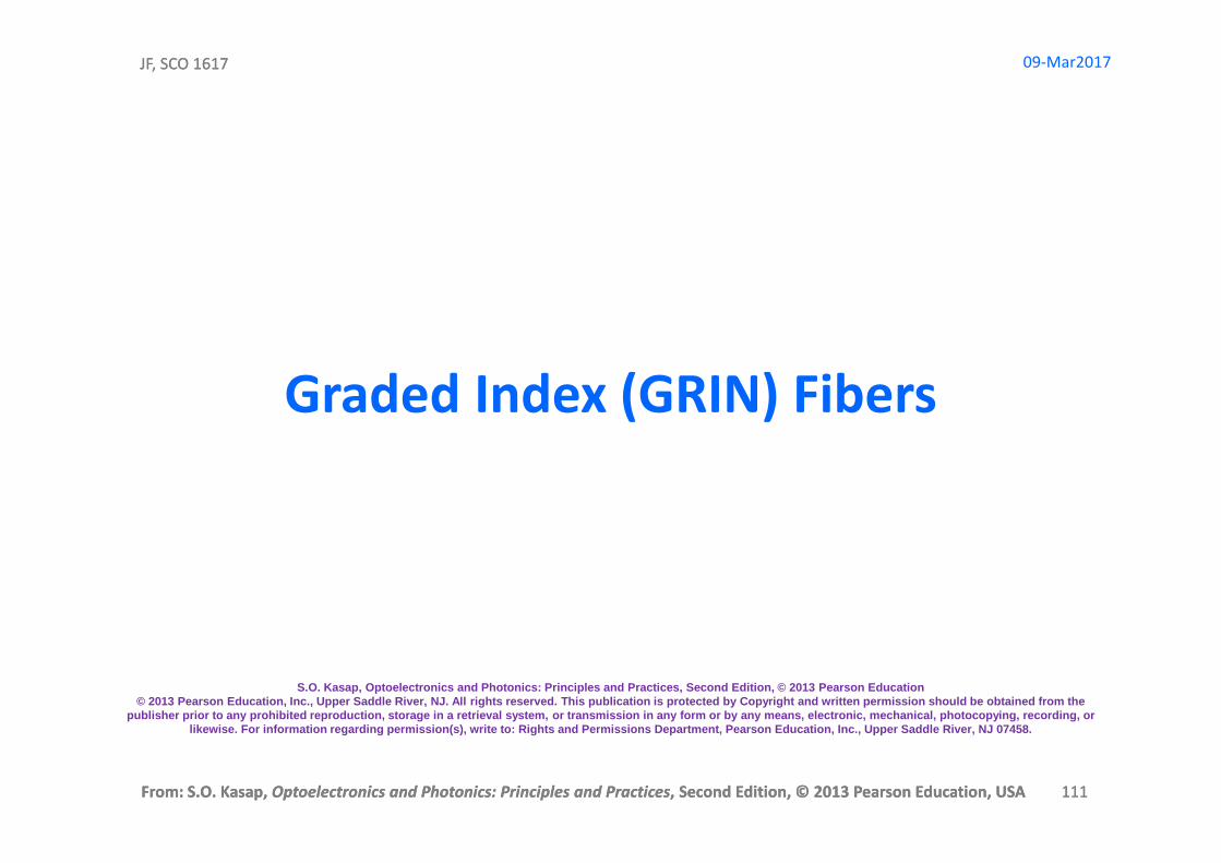
Graded Index (GRIN) Fiber
(a) Multimode step
index fiber. Ray
paths are
different so that
rays arrive at
different times.
(b) Graded index
fiber. Ray paths
are different but
so are the
velocities along
the paths so
that all the rays
arrive at the
same time.

From: S.O. Kasap, Optoelectronics and Photonics: Principles and Practices, Second Edition, © 2013 Pearson Education, USA 113
JF, SCO 1617
From: S.O. Kasap, Optoelectronics and Photonics: Principles and Practices, Second Edition, © 2013 Pearson Education, USA 113
JF, SCO 1617
(a) A ray in thinly stratifed medium becomes refracted as it passes from one layer to the next upper layer with lower nand eventually its angle satisfies TIR.
(b) In a medium where n decreases continuously the path of the ray bends continuously.
Graded Index (GRIN) Fiber

From: S.O. Kasap, Optoelectronics and Photonics: Principles and Practices, Second Edition, © 2013 Pearson Education, USA 114
JF, SCO 1617
From: S.O. Kasap, Optoelectronics and Photonics: Principles and Practices, Second Edition, © 2013 Pearson Education, USA 114
JF, SCO 1617
Graded Index (GRIN) Fiber
The refractive index profile cangenerally be described by a power lawwith an indexγ called theprofile index(or the coefficient of index grating) sothat,
n = n1[1 − 2∆(r/a)γ]1/2 ; r < a,
n = n2 ; r ≥ a
σ intermode
L≈ n1
20 3c∆2
Minimum intermodal dispersion
Minimum intermodal dispersion
225
)3)(4(2 ≈
+++∆−+≈
δδδδγ o

From: S.O. Kasap, Optoelectronics and Photonics: Principles and Practices, Second Edition, © 2013 Pearson Education, USA 115
JF, SCO 1617
From: S.O. Kasap, Optoelectronics and Photonics: Principles and Practices, Second Edition, © 2013 Pearson Education, USA 115
JF, SCO 1617
Graded Index (GRIN) Fiber
σ intermode
L≈ n1
20 3c∆2
Minimum intermodal dispersion
Minimum intermodal dispersion
225
)3)(4(2 ≈
+++∆−+≈
δδδδγ o
λλδ
d
d
N
n ∆
∆−=
1
1
g
Profile dispersion parameter
From: S.O. Kasap, Optoelectronics and Photonics: Principles and Practices, Second Edition, © 2013 Pearson Education, USA 116
JF, SCO 1617
From: S.O. Kasap, Optoelectronics and Photonics: Principles and Practices, Second Edition, © 2013 Pearson Education, USA 116
JF, SCO 1617
Graded Index (GRIN) Fiber
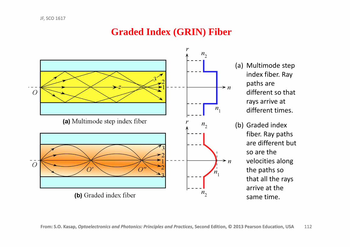
2/122
2 ])([)(NANA nrnr −==
2/122
21
2/1GRIN ))(2/1(NA nn −≈
Effective numerical aperture for GRIN fibers
22
2VM
+≈
γγ
Number of modes in a graded index fiber

From: S.O. Kasap, Optoelectronics and Photonics: Principles and Practices, Second Edition, © 2013 Pearson Education, USA 117
JF, SCO 1617
Table 2.5
Graded index multimode fibers
d = core diameter (µm), D = cladding diameter (µm). Typical properties at 850 nm. VCSEL is a
vertical cavity surface emitting laser. α is attenuation along the fiber. OM1, OM3 and OM4 are
fiber standards for LAN data links (ethernet). α are reported typical attenuation values. 10G and
40G networks represent data rates of 10 Gb s-1 and 40 Gb s-1 and correspond to 10 GbE (Gigabit
Ethernet) and 40 GbE systems.
MMF d/D
Compliance standard
Source Typical Dch
ps nm-1 km-1
Bandwidth
MHz⋅km
ΝΑ α
dB km-1
Reach in 10G and 40G networks
50/125 OM4 VCSEL −100 4700 (EMB)
3500 (OFLBW)
0.200 < 3 550 m (10G)
150 m (40G)
50/125 OM3 VCSEL −100 2000 (EMB)
500 (OFLBW)
0.200 < 3 300 m (10G)
62.5/125 OM1 LED −117 200 (OFLBW) 0.275 < 3 33 m (10G)
From: S.O. Kasap, Optoelectronics and Photonics: Principles and Practices, Second Edition, © 2013 Pearson Education, USA 118
JF, SCO 1617
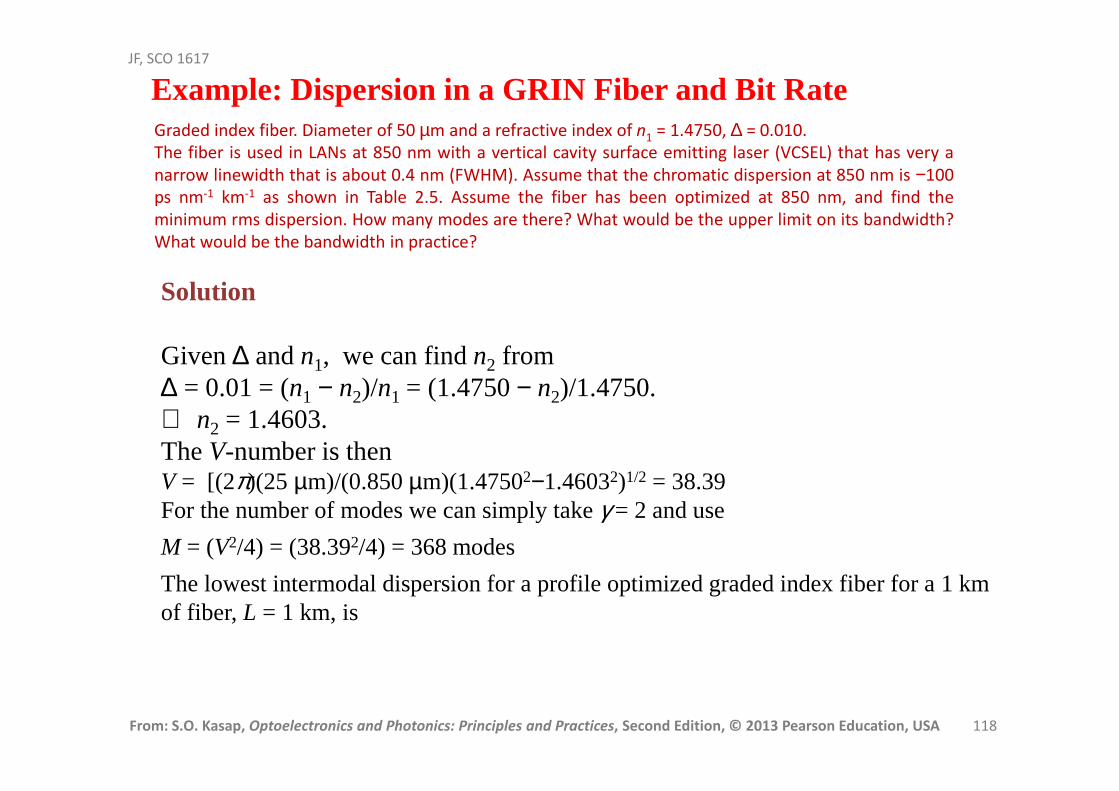
Example: Dispersion in a GRIN Fiber and Bit RateGraded index fiber. Diameter of 50 µm and a refractive index of n1 = 1.4750, ∆ = 0.010.
The fiber is used in LANs at 850 nm with a vertical cavity surface emitting laser (VCSEL) that has very a
narrow linewidth that is about 0.4 nm (FWHM). Assume that the chromatic dispersion at 850 nm is −100
ps nm-1 km-1 as shown in Table 2.5. Assume the fiber has been optimized at 850 nm, and find the
minimum rms dispersion. How many modes are there? What would be the upper limit on its bandwidth?
What would be the bandwidth in practice?
Solution
Given ∆ and n1, we can find n2 from ∆ = 0.01 = (n1 − n2)/n1 = (1.4750 − n2)/1.4750. ∴ n2 = 1.4603. The V-number is thenV = [(2π)(25 µm)/(0.850 µm)(1.47502−1.46032)1/2 = 38.39For the number of modes we can simply take γ = 2 and use
M = (V2/4) = (38.392/4) = 368 modes
The lowest intermodal dispersion for a profile optimized graded index fiber for a 1 km of fiber, L = 1 km, is
From: S.O. Kasap, Optoelectronics and Photonics: Principles and Practices, Second Edition, © 2013 Pearson Education, USA 119
JF, SCO 1617
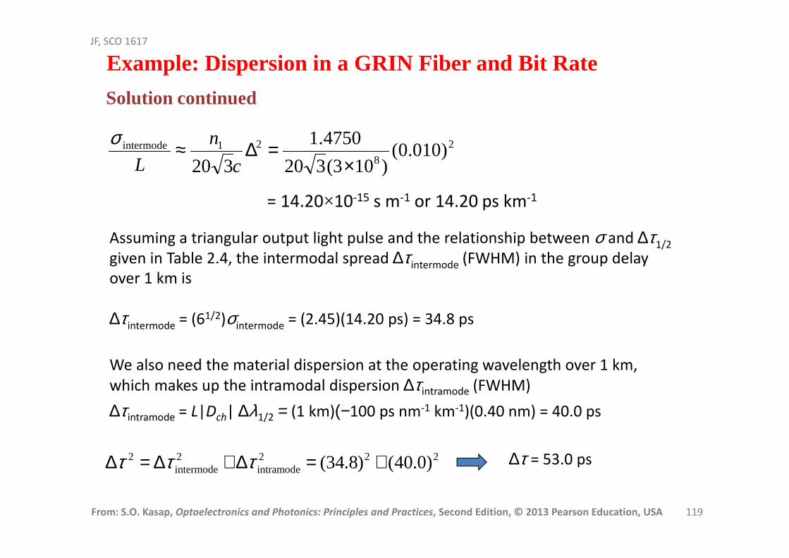
Example: Dispersion in a GRIN Fiber and Bit Rate
Solution continued
2
8
21intermode )010.0()103(320
4750.1
320 ×=∆≈
c
n
L
σ
= 14.20×10⁻¹⁵ s m-1 or 14.20 ps km-1
Assuming a triangular output light pulse and the relationship between σ and ∆τ1/2
given in Table 2.4, the intermodal spread ∆τintermode (FWHM) in the group delay
over 1 km is
∆τintermode = (61/2)σintermode = (2.45)(14.20 ps) = 34.8 ps
We also need the material dispersion at the operating wavelength over 1 km,
which makes up the intramodal dispersion ∆τintramode (FWHM)
∆τintramode = L|Dch| ∆λ1/2 = (1 km)(−100 ps nm-1 km-1)(0.40 nm) = 40.0 ps
222intramode
2intermode
2 )0.40()8.34( +=∆+∆=∆ τττ ∆τ = 53.0 ps
From: S.O. Kasap, Optoelectronics and Photonics: Principles and Practices, Second Edition, © 2013 Pearson Education, USA 120
JF, SCO 1617
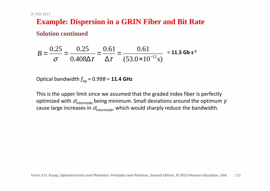
Example: Dispersion in a GRIN Fiber and Bit Rate
Solution continued
)s100.53(
61.061.0
408.0
25.025.012−×
=∆
=∆
==ττσ
B = 11.5 Gb s-1
Optical bandwidth fop = 0.99B = 11.4 GHz
This is the upper limit since we assumed that the graded index fiber is perfectly
optimized with σintermode being minimum. Small deviations around the optimum γcause large increases in σintermode, which would sharply reduce the bandwidth.

From: S.O. Kasap, Optoelectronics and Photonics: Principles and Practices, Second Edition, © 2013 Pearson Education, USA 121
JF, SCO 1617
Example: Dispersion in a GRIN Fiber and Bit Rate
Solution continued
If this were a multimode step-index fiber with the same n1 and n2, then the full
dispersion (total spread) would roughly be
8121
103
)01.0)(475.1(
×=∆=−≈∆
c
n
c
nn
L
τ
= 4.92×10⁻¹¹ s m-1 or 49.2 ns km-1
To calculate the BL we use σintermode ≈ 0.29∆τ
)km s 102.49)(29.0(
25.0
)/(29.0
25.025.019
intermode−−×
=∆
=≈L
LBL
τσ= 17.5 Mb s-1 km
LANs now use graded index MMFs, and the step index MMFs are used mainly in low speed instrumentation

From: S.O. Kasap, Optoelectronics and Photonics: Principles and Practices, Second Edition, © 2013 Pearson Education, USA 122
JF, SCO 1617
From: S.O. Kasap, Optoelectronics and Photonics: Principles and Practices, Second Edition, © 2013 Pearson Education, USA 122
JF, SCO 1617
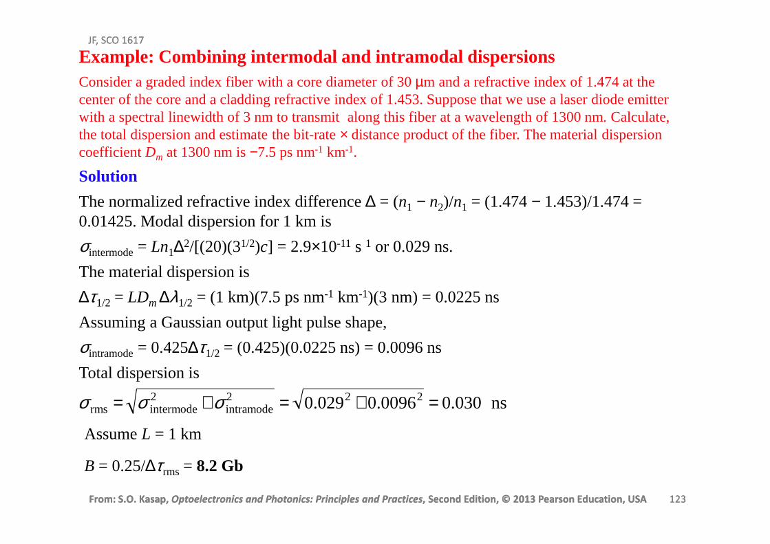
Example: Dispersion in a graded-index fiber and bit rate
Consider a graded index fiber whose core has a diameter of 50 µm and a refractive index of n1 = 1.480. The cladding has n2 = 1.460. If this fiber is used at 1.30 µm with a laser diode that has very a narrow linewidth what will be the bit rate× distance product? Evaluate the BL product if this were a multimode step index fiber.
Solution The normalized refractive index difference ∆ = (n1 − n2)/n1 = (1.48 − 1.46)/1.48 = 0.0135. Dispersion for 1 km of fiber is
σintermode/L = n1∆2/[(20)(31/2)c] = 2.6×10⁻¹⁴ s m-1 or 0.026 ns km-1.
BL = 0.25/σintermode= 9.6 Gb s-1 km
We have ignored any material dispersion and, further, we assumed the index variation to perfectly follow the optimal profile which means that in practice BL will be worse. (For example, a 15% variation in γ from the optimal value can result in σintermodeand hence BLthat are more than 10 times worse.)
If this were a multimode step-index fiber with the same n1 and n2, then the full dispersion (total spread) would roughly be 6.67×10⁻¹¹ s m-1 or 66.7 ns km-1 and BL = 12.9 Mb s-1 km
Note:Over long distances, the bit rate × distance product is not constant for multimode fibers and typically B ∝ L−γ where γ is an index between 0.5 and 1. The reason is that, due to various fiber imperfections, there is mode mixing which reduces the extent of spreading.
From: S.O. Kasap, Optoelectronics and Photonics: Principles and Practices, Second Edition, © 2013 Pearson Education, USA 123
JF, SCO 1617
From: S.O. Kasap, Optoelectronics and Photonics: Principles and Practices, Second Edition, © 2013 Pearson Education, USA 123
JF, SCO 1617
Example: Combining intermodal and intramodal dispersionsConsider a graded index fiber with a core diameter of 30 µm and a refractive index of 1.474 at the center of the core and a cladding refractive index of 1.453. Suppose that we use a laser diode emitter with a spectral linewidth of 3 nm to transmit along this fiber at a wavelength of 1300 nm. Calculate, the total dispersion and estimate the bit-rate× distance product of the fiber. The material dispersion coefficient Dm at 1300 nm is −7.5 ps nm-1 km-1.
Solution
The normalized refractive index difference ∆ = (n1 − n2)/n1 = (1.474 − 1.453)/1.474 = 0.01425. Modal dispersion for 1 km is
σintermode= Ln1∆2/[(20)(31/2)c] = 2.9×10⁻¹¹ s 1 or 0.029 ns.
The material dispersion is
∆τ1/2 = LDm ∆λ1/2 = (1 km)(7.5 ps nm-1 km-1)(3 nm) = 0.0225 ns
Assuming a Gaussian output light pulse shape,
σintramode= 0.425∆τ1/2 = (0.425)(0.0225 ns) = 0.0096 ns
Total dispersion is
σ rms = σ intermode2 +σ intramode
2 = 0.0292 + 0.00962 = 0.030 ns
B = 0.25/∆τrms = 8.2 Gb
Assume L = 1 km
From: S.O. Kasap, Optoelectronics and Photonics: Principles and Practices, Second Edition, © 2013 Pearson Education, USA 124
JF, SCO 1617
From: S.O. Kasap, Optoelectronics and Photonics: Principles and Practices, Second Edition, © 2013 Pearson Education, USA 124
JF, SCO 1617
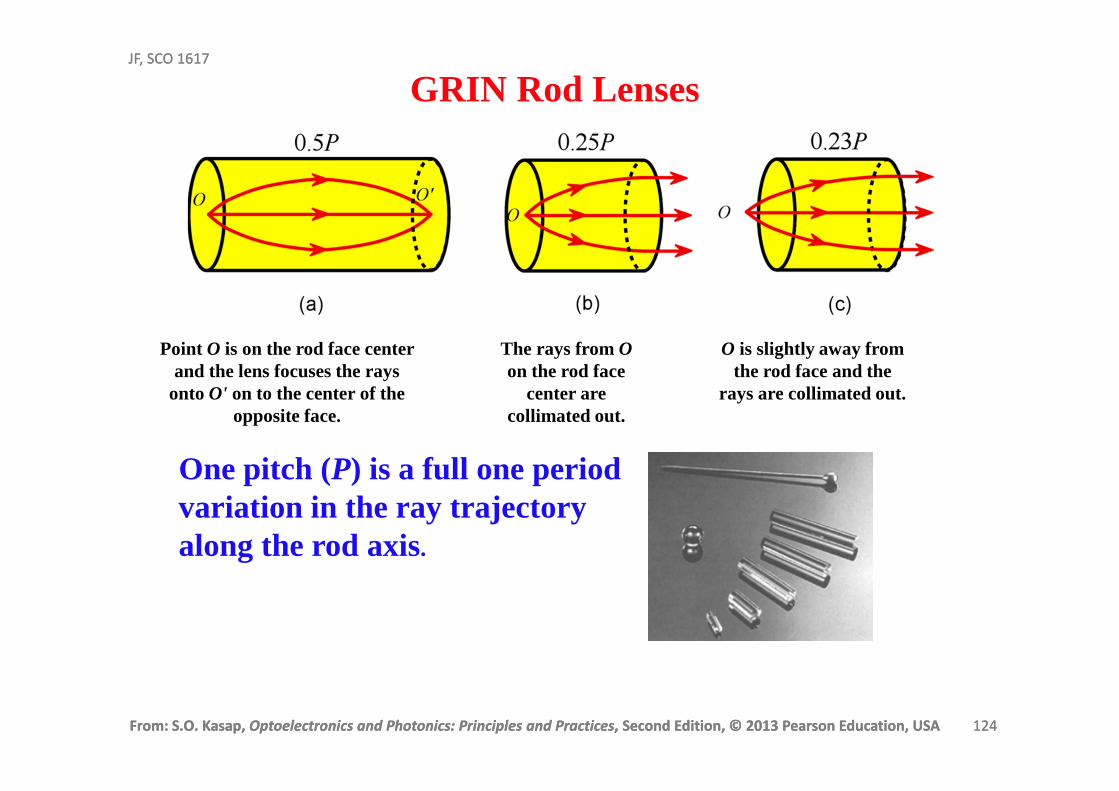
GRIN Rod Lenses
Point O is on the rod face center and the lens focuses the rays
onto O' on to the center of the opposite face.
One pitch (P) is a full one period variation in the ray trajectory along the rod axis.
The rays from Oon the rod face
center are collimated out.
O is slightly away from the rod face and the
rays are collimated out.
From: S.O. Kasap, Optoelectronics and Photonics: Principles and Practices, Second Edition, © 2013 Pearson Education, USA 125
JF, SCO 1617
From: S.O. Kasap, Optoelectronics and Photonics: Principles and Practices, Second Edition, © 2013 Pearson Education, USA 125
JF, SCO 1617
Chapter 2 Dielectric Waveguides and Optical Fibers
Charles Kao, Nobel Laureate (2009)Courtesy of the Chinese University of Hong Kong
Losses in optical fibers
S.O. Kasap, Optoelectronics and Photonics: Principles and Practices, Second Edition, © 2013 Pearson Education© 2013 Pearson Education, Inc., Upper Saddle River, NJ. All rights reserved. This publication is prote cted by Copyright and written permission should be obtained from the
publisher prior to any prohibited reproduction, sto rage in a retrieval system, or transmission in any form or by any means, electronic, mechanical, photo copying, recording, or likewise. For information regarding permission(s), write to: Rights and Permissions Department, Pearso n Education, Inc., Upper Saddle River, NJ 07458.
14-Fev-2017
From: S.O. Kasap, Optoelectronics and Photonics: Principles and Practices, Second Edition, © 2013 Pearson Education, USA 126
JF, SCO 1617
From: S.O. Kasap, Optoelectronics and Photonics: Principles and Practices, Second Edition, © 2013 Pearson Education, USA 126
JF, SCO 1617
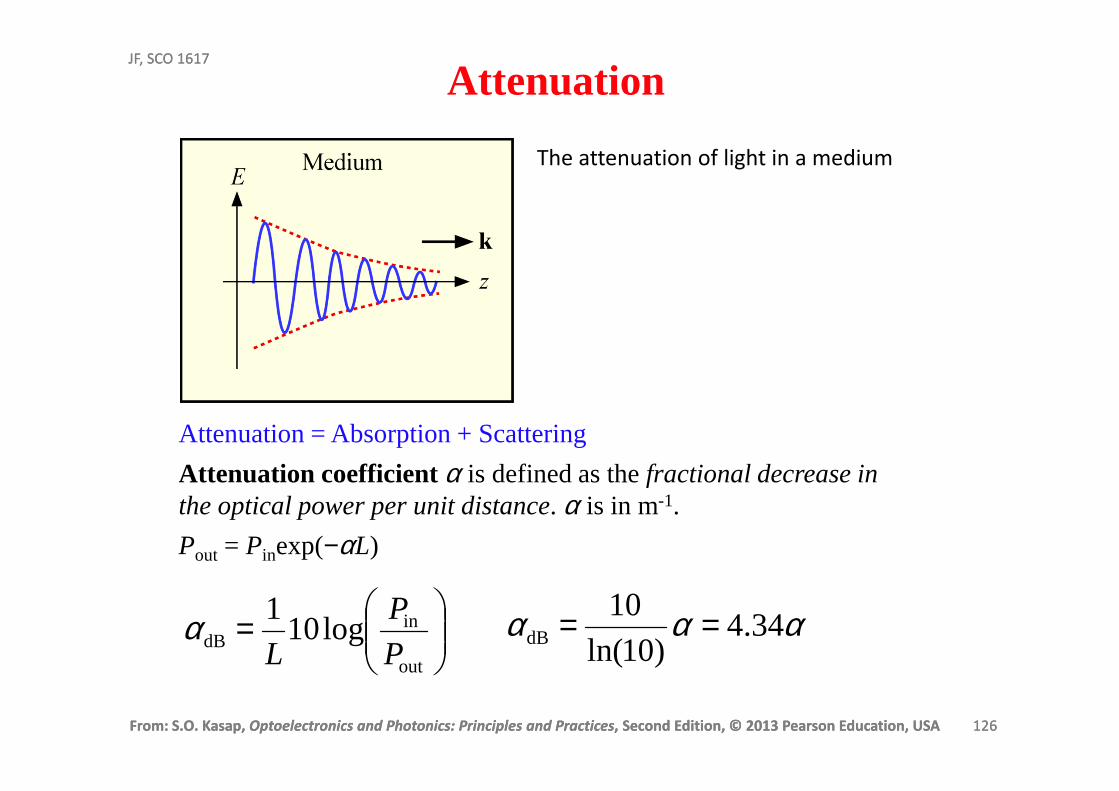
Attenuation
Attenuation = Absorption + Scattering
Attenuation coefficient α is defined as the fractional decrease in the optical power per unit distance. α is in m-1.
Pout = Pinexp(−αL)
=
out
indB log10
1
P
P
Lα ααα 34.4
)10ln(
10dB ==
The attenuation of light in a medium
From: S.O. Kasap, Optoelectronics and Photonics: Principles and Practices, Second Edition, © 2013 Pearson Education, USA 127
JF, SCO 1617
From: S.O. Kasap, Optoelectronics and Photonics: Principles and Practices, Second Edition, © 2013 Pearson Education, USA 127
JF, SCO 1617
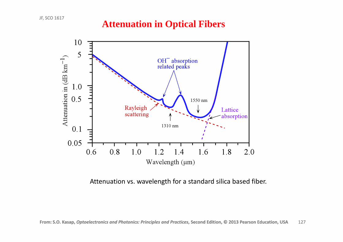
Attenuation in Optical Fibers
Attenuation vs. wavelength for a standard silica based fiber.
From: S.O. Kasap, Optoelectronics and Photonics: Principles and Practices, Second Edition, © 2013 Pearson Education, USA 128
JF, SCO 1617
From: S.O. Kasap, Optoelectronics and Photonics: Principles and Practices, Second Edition, © 2013 Pearson Education, USA 128
JF, SCO 1617
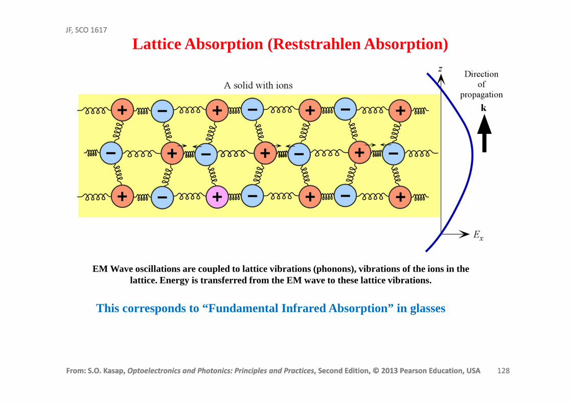
Lattice Absorption (Reststrahlen Absorption)
EM Wave oscillations are coupled to lattice vibrations (phonons), vibrations of the ions in the lattice. Energy is transferred from the EM wave to these lattice vibrations.
This corresponds to “Fundamental Infrared Absorption” in glasses
From: S.O. Kasap, Optoelectronics and Photonics: Principles and Practices, Second Edition, © 2013 Pearson Education, USA 129
JF, SCO 1617
From: S.O. Kasap, Optoelectronics and Photonics: Principles and Practices, Second Edition, © 2013 Pearson Education, USA 129
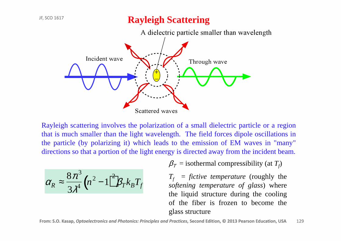
JF, SCO 1617 Rayleigh Scattering
Rayleigh scattering involves the polarization of a small dielectric particle or a regionthat is much smaller than the light wavelength. The field forces dipole oscillations inthe particle (by polarizing it) which leads to the emission of EM waves in"many"directions so that a portion of the light energy is directed away from the incident beam.
αR ≈ 8π 3
3λ4 n2 −1( )2βTkBTf
βΤ = isothermal compressibility (atTf)
Tf = fictive temperature(roughly thesoftening temperature of glass) wherethe liquid structure during the coolingof the fiber is frozen to become theglass structure
From: S.O. Kasap, Optoelectronics and Photonics: Principles and Practices, Second Edition, © 2013 Pearson Education, USA 130
JF, SCO 1617
From: S.O. Kasap, Optoelectronics and Photonics: Principles and Practices, Second Edition, © 2013 Pearson Education, USA 130
JF, SCO 1617
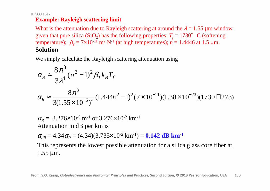
Example: Rayleigh scattering limit
What is the attenuation due to Rayleigh scattering at around the λ = 1.55 µm window given that pure silica (SiO2) has the following properties: Tf = 1730°C (softening temperature); βT = 7×10-11 m2 N-1 (at high temperatures); n = 1.4446 at 1.5 µm.SolutionWe simply calculate the Rayleigh scattering attenuation using
αR ≈ 8π 3
3λ4 (n2 −1)2βTkBTf
αR ≈ 8π 3
3(1.55×10⁻⁶)4 (1.44462 −1)2(7×10⁻¹¹)(1.38×10⁻²³)(1730+ 273)
αR = 3.276×10⁻⁵ m-1 or 3.276×10⁻² km-1
Attenuation in dB per km is
αdB = 4.34αR = (4.34)(3.735×10⁻² km-1) = 0.142 dB km-1
This represents the lowest possible attenuation for a silica glass core fiber at 1.55 µm.

From: S.O. Kasap, Optoelectronics and Photonics: Principles and Practices, Second Edition, © 2013 Pearson Education, USA 131
JF, SCO 1617
From: S.O. Kasap, Optoelectronics and Photonics: Principles and Practices, Second Edition, © 2013 Pearson Education, USA 131
JF, SCO 1617
Attenuation in Optical Fibers
Attenuation vs. wavelength for a standard silica based fiber.
From: S.O. Kasap, Optoelectronics and Photonics: Principles and Practices, Second Edition, © 2013 Pearson Education, USA 132
JF, SCO 1617
From: S.O. Kasap, Optoelectronics and Photonics: Principles and Practices, Second Edition, © 2013 Pearson Education, USA 132
JF, SCO 1617
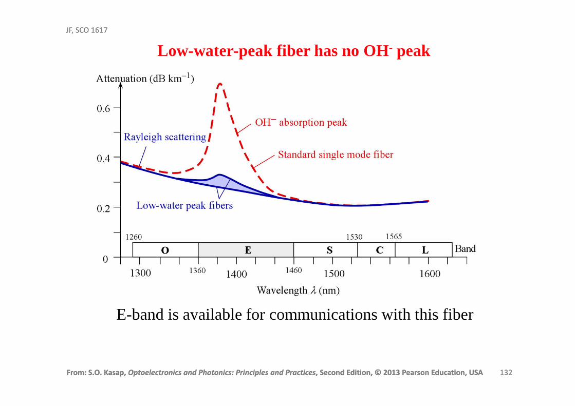
Low-water-peak fiber has no OH- peak
E-band is available for communications with this fiber

From: S.O. Kasap, Optoelectronics and Photonics: Principles and Practices, Second Edition, © 2013 Pearson Education, USA 133
JF, SCO 1617
From: S.O. Kasap, Optoelectronics and Photonics: Principles and Practices, Second Edition, © 2013 Pearson Education, USA 133
JF, SCO 1617
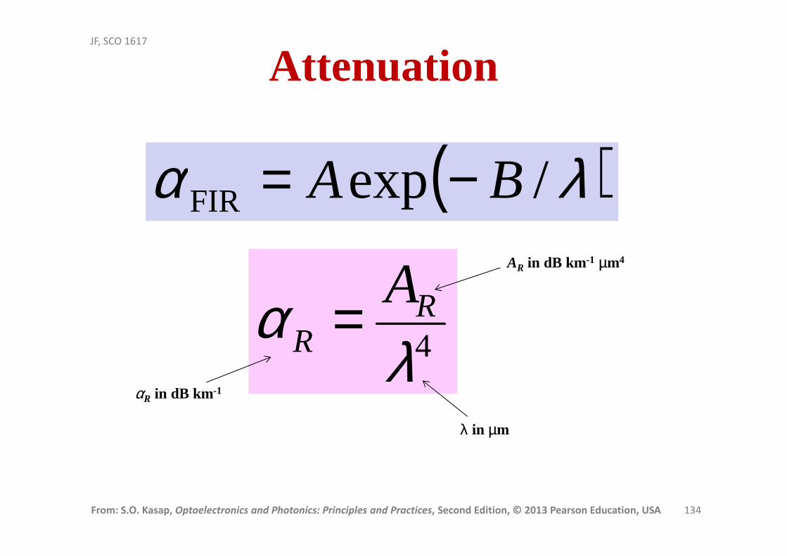
( )λα /expFIR BA −=4λ
α RR
A=
Attenuation in Optical Fibers
From: S.O. Kasap, Optoelectronics and Photonics: Principles and Practices, Second Edition, © 2013 Pearson Education, USA 134
JF, SCO 1617
Attenuation
( )λα /expFIR BA −=
4λα R
R
A=AR in dB km-1 µm4
λ in µm
αR in dB km-1

From: S.O. Kasap, Optoelectronics and Photonics: Principles and Practices, Second Edition, © 2013 Pearson Education, USA 135
JF, SCO 1617
Attenuation
Glass AR
dB km-1 µm4
Comment Glass
Silica fiber 0.90 "Rule of thumb" Silica fiber
SiO2-GeO2 core step index fiber
0.63 + 2.06×NA NA depends on (n12 – n2
2)1/2
and hence on the doping difference.
SiO2-GeO2 core step index fiber
SiO2-GeO2 core graded index fiber
0.63 + 1.75×NA SiO2-GeO2 core graded index fiber
Silica, SiO2 0.63 Measured on preforms. Depends on annealing. AR(Silica) = 0.59 dB km-1 µm4
for annealed.
Silica, SiO2
65%SiO235%GeO2 0.75 On a preform. AR/AR(silica) = 1.19
65%SiO235%GeO2
(SiO2)1−x(GeO2)x AR(silica)×(1 + 0.62x) x = [GeO2] = Concentration as a fraction (10% GeO2, x = 0.1). For preform.
(SiO2)1−x(GeO2)x
Approximate attenuation coefficients for silica-based fibers for use in Equations (7) and (8). Squarebrackets represent concentration as a fraction. NA = Numerical Aperture. AR = 0.59 used as referencefor pure silica, and representsAR(silica). Data mainly from K. Tsujikawa et al, Electron. Letts., 30, 351,1994; Opt. Fib. Technol. 11, 319, 2005, H. Hughes,Telecommunications Cables(John Wiley and Sons,1999, and references therein.)
From: S.O. Kasap, Optoelectronics and Photonics: Principles and Practices, Second Edition, © 2013 Pearson Education, USA 136
JF, SCO 1617
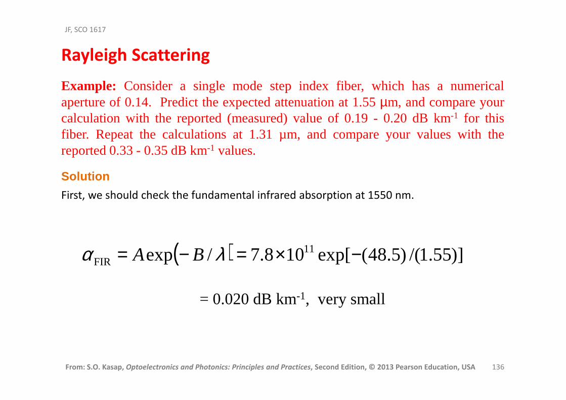
Rayleigh Scattering
Example: Consider a single mode step index fiber, which has a numericalaperture of 0.14. Predict the expected attenuation at 1.55µm, and compare yourcalculation with the reported (measured) value of 0.19 - 0.20 dB km-1 for thisfiber. Repeat the calculations at 1.31 µm, and compare your values with thereported 0.33 - 0.35 dB km-1 values.
( ) )]55.1/()5.48(exp[108.7/exp 11FIR −×=−= λα BA
Solution
First, we should check the fundamental infrared absorption at 1550 nm.
= 0.020 dB km-1, very small
From: S.O. Kasap, Optoelectronics and Photonics: Principles and Practices, Second Edition, © 2013 Pearson Education, USA 137
JF, SCO 1617
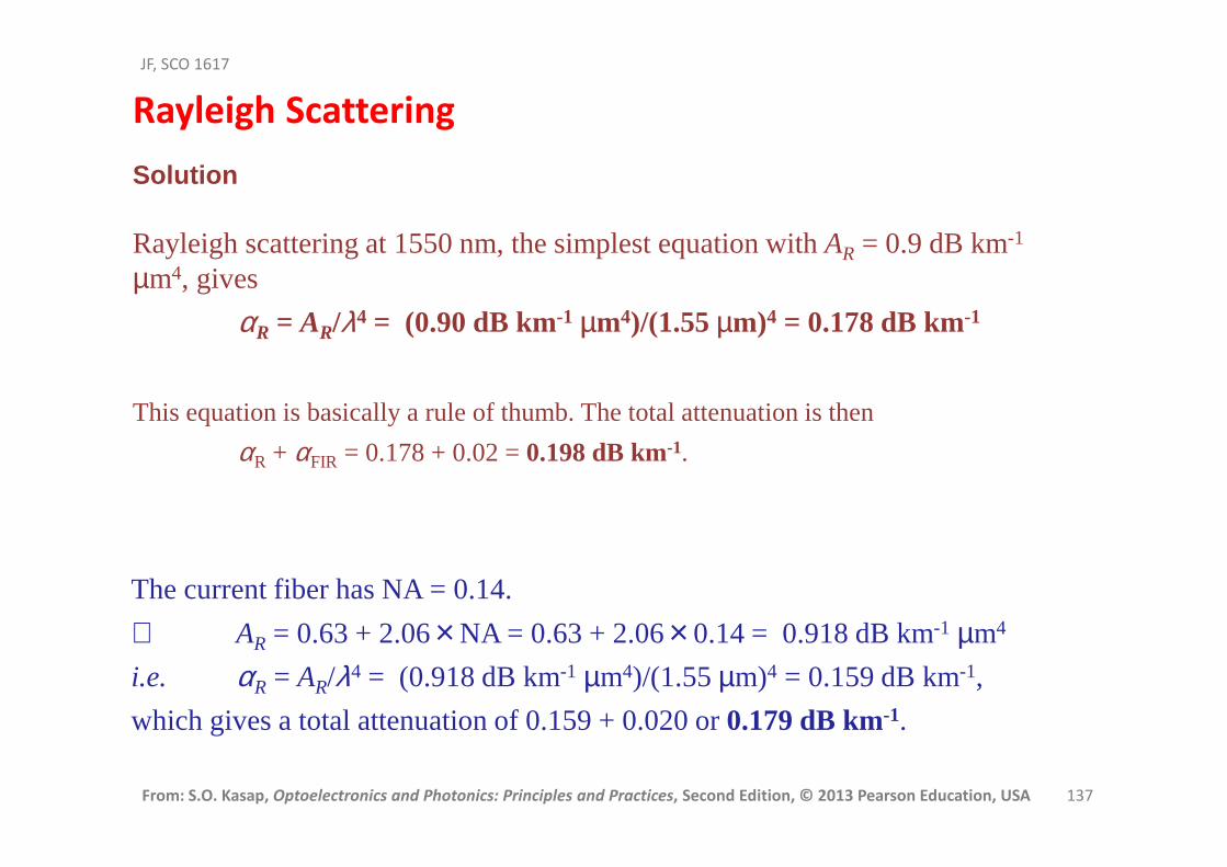
Solution
Rayleigh scattering at 1550 nm, the simplest equation with AR = 0.9 dB km-1
µm4, gives
αR = AR/λ4 = (0.90 dB km-1 µm4)/(1.55 µm)4 = 0.178 dB km-1
This equation is basically a rule of thumb. The total attenuation is then
αR + αFIR = 0.178 + 0.02 = 0.198 dB km-1.
The current fiber has NA = 0.14.
∴ AR = 0.63 + 2.06×NA = 0.63 + 2.06×0.14 = 0.918 dB km-1 µm4
i.e. αR = AR/λ4 = (0.918 dB km-1 µm4)/(1.55 µm)4 = 0.159 dB km-1,
which gives a total attenuation of 0.159 + 0.020 or0.179 dB km-1.
Rayleigh Scattering
From: S.O. Kasap, Optoelectronics and Photonics: Principles and Practices, Second Edition, © 2013 Pearson Education, USA 138
JF, SCO 1617
Solution
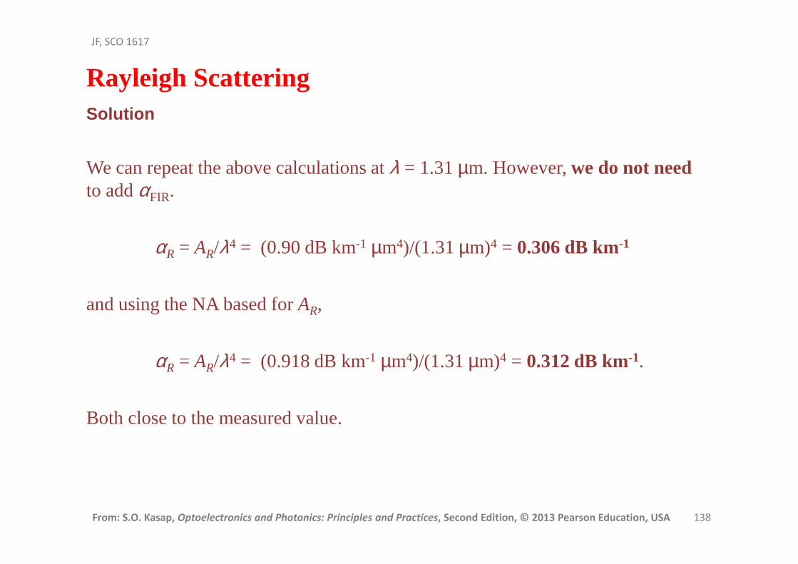
We can repeat the above calculations at λ = 1.31 µm. However, we do not need to add αFIR.
αR = AR/λ4 = (0.90 dB km-1 µm4)/(1.31 µm)4 = 0.306 dB km-1
and using the NA based for AR,
αR = AR/λ4 = (0.918 dB km-1 µm4)/(1.31 µm)4 = 0.312 dB km-1.
Both close to the measured value.
Rayleigh Scattering

From: S.O. Kasap, Optoelectronics and Photonics: Principles and Practices, Second Edition, © 2013 Pearson Education, USA 139
JF, SCO 1617
Bending Loss
Definitions of (a) microbending and (b) macrobending loss and the definition of the radius of curvature, R. (A schematic illustration only.) The propagating mode in the fiber is shown as white painted area. Some radiation is lost in the region
where the fiber is bent. D is the fiber diameter, including the cladding.

From: S.O. Kasap, Optoelectronics and Photonics: Principles and Practices, Second Edition, © 2013 Pearson Education, USA 140
JF, SCO 1617 Bending Loss
Microbending loss
the radius of curvature R of the bend is sharp
bend radius is comparable to the diameter of the fiber
Typically microbending losses are significant when the radius of curvature of
the bend is less than 0.1 − 1 mm.
They can arise from careless or poor cabling of the fiber or even in flaws in
manufacturing that result in variations in the fiber geometry over small
distances.

From: S.O. Kasap, Optoelectronics and Photonics: Principles and Practices, Second Edition, © 2013 Pearson Education, USA 141
JF, SCO 1617
Bending Loss
Macrobending lossesLosses that arise when the bend is much larger than the fiber size
Typically much grater than 1 mm
Typically occur when the fiber is bent during the installation of a fiber optic link such as turning the fiber around a corner.
There is no simple precise and sharp boundary line between microbending andmacrobending loss definitions.
Both losses essentially result from changes in the waveguide geometry and properties asthe fiber is subjected to external forces that bend the fiber.
Typically, macrobending loss crosses over into microbending loss when the radius ofcurvature becomes less than a few millimeters.

From: S.O. Kasap, Optoelectronics and Photonics: Principles and Practices, Second Edition, © 2013 Pearson Education, USA 142
JF, SCO 1617
From: S.O. Kasap, Optoelectronics and Photonics: Principles and Practices, Second Edition, © 2013 Pearson Education, USA 142
JF, SCO 1617 Bending Loss
Sharp bends change the local waveguide geometry that can lead to waves escaping. The zigzagging ray suddenly finds itself with an incidence angle smaller than θ′ that gives rise to either a transmitted wave, or to a greater cladding penetration; the field reaches
the outside medium and some light energy is lost.

From: S.O. Kasap, Optoelectronics and Photonics: Principles and Practices, Second Edition, © 2013 Pearson Education, USA 143
JF, SCO 1617
From: S.O. Kasap, Optoelectronics and Photonics: Principles and Practices, Second Edition, © 2013 Pearson Education, USA 143
JF, SCO 1617
Bending Loss
When a fiber is bent sharply, the propagating wavefront along the straight fiber cannot bend around and continue as a wavefront because a portion of it (black shaded) beyond the critical radial distance rc must travel faster than the speed of light in vacuum. This portion is lost in the cladding- radiated away.
From: S.O. Kasap, Optoelectronics and Photonics: Principles and Practices, Second Edition, © 2013 Pearson Education, USA 144
JF, SCO 1617
From: S.O. Kasap, Optoelectronics and Photonics: Principles and Practices, Second Edition, © 2013 Pearson Education, USA 144
JF, SCO 1617 Bending Loss
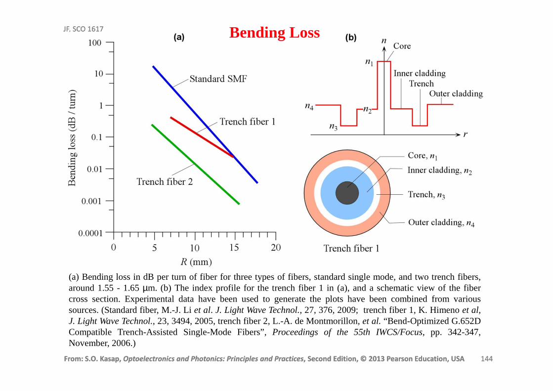
(a) Bending loss in dB per turn of fiber for three types of fibers, standard single mode, and two trench fibers,around 1.55 - 1.65µm. (b) The index profile for the trench fiber 1 in (a), and a schematic view of the fibercross section. Experimental data have been used to generatethe plots have been combined from varioussources. (Standard fiber, M.-J. Liet al. J. Light Wave Technol., 27, 376, 2009; trench fiber 1, K. Himenoet al,J. Light Wave Technol., 23, 3494, 2005, trench fiber 2, L.-A. de Montmorillon,et al. “Bend-Optimized G.652DCompatible Trench-Assisted Single-Mode Fibers”,Proceedings of the 55th IWCS/Focus, pp. 342-347,November, 2006.)
From: S.O. Kasap, Optoelectronics and Photonics: Principles and Practices, Second Edition, © 2013 Pearson Education, USA 145
JF, SCO 1617
Bend Insensitive Fibers
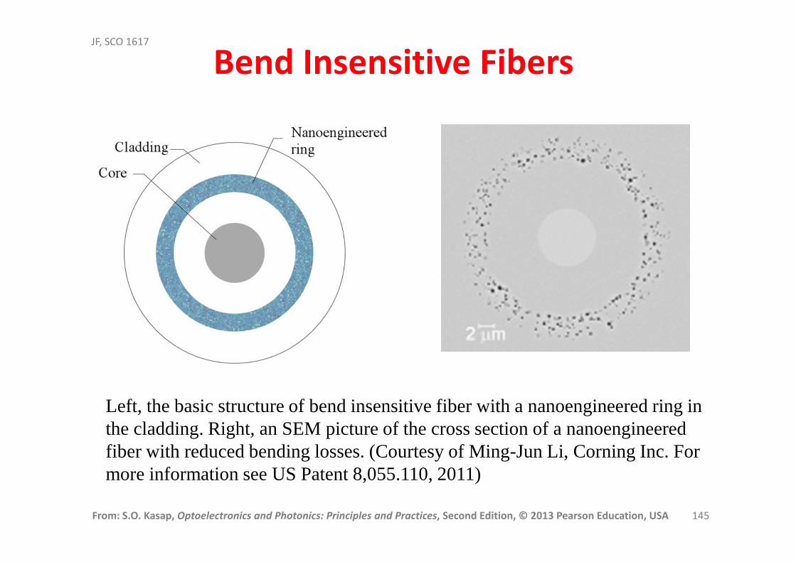
Left, the basic structure of bend insensitive fiber with a nanoengineered ring in the cladding. Right, an SEM picture of the cross section of a nanoengineered fiber with reduced bending losses. (Courtesy of Ming-Jun Li, Corning Inc. For more information see US Patent 8,055.110, 2011)

From: S.O. Kasap, Optoelectronics and Photonics: Principles and Practices, Second Edition, © 2013 Pearson Education, USA 146
JF, SCO 1617
Bending Loss in Fibers
General Description
αB = Aexp(−R/Rc)
A and Rc are constants

From: S.O. Kasap, Optoelectronics and Photonics: Principles and Practices, Second Edition, © 2013 Pearson Education, USA 147
JF, SCO 1617
From: S.O. Kasap, Optoelectronics and Photonics: Principles and Practices, Second Edition, © 2013 Pearson Education, USA 147
JF, SCO 1617
Bending Loss αB = Aexp(−R/Rc)
where A and Rc are constants
For single mode fibers, a quantity called a MAC-value, or a MAC-number, NMAC, has been used to characterize the bending loss. NMAC
is defined by
c
Nλ
MFD
h wavelengtoff-Cut
diameter fieldModeMAC ==

From: S.O. Kasap, Optoelectronics and Photonics: Principles and Practices, Second Edition, © 2013 Pearson Education, USA 148
JF, SCO 1617
From: S.O. Kasap, Optoelectronics and Photonics: Principles and Practices, Second Edition, © 2013 Pearson Education, USA 148
JF, SCO 1617
∆−∝
−∝ − 2/3
expexpR
R
R
c
α
Microbending Loss
Measured microbending loss for a 10 cm fiber bent by different amounts of radius of curvature R. Single mode fiber with a core diameter of 3.9 µm, cladding radius 48 µm, ∆ = 0.00275, NA ≈ 0.10, V ≈ 1.67 and 2.08. Data extracted from A.J. Harris and P.F. Castle, "Bend Loss Measurements on High Aperture Single-Mode Fibers as a Function of Wavelength and Bend Radius", IEEE J. Light Wave Technology,Vol. LT14, 34, 1986, and repotted with a smoothed curve; see original article for the discussion of peaks in αB vs. R at 790 nm).

From: S.O. Kasap, Optoelectronics and Photonics: Principles and Practices, Second Edition, © 2013 Pearson Education, USA 149
JF, SCO 1617
Bending Loss in SMF
αB = Aexp(−R/Rc)
MAC -value, or a MAC-number, NMAC
c
Nλ
MFD
h wavelengtoff-Cut
diameter fieldModeMAC ==
NOTES
αB increases with increasing MFD
αB decreasing cut-off wavelength.
αB increases exponentially with the MAC-number
It is not a universal function, and different types of fibers, with very different refractive index profiles, can exhibit different αB−NMAC behavior.
NMAC values are typically in the range 6− 8
From: S.O. Kasap, Optoelectronics and Photonics: Principles and Practices, Second Edition, © 2013 Pearson Education, USA 150
JF, SCO 1617
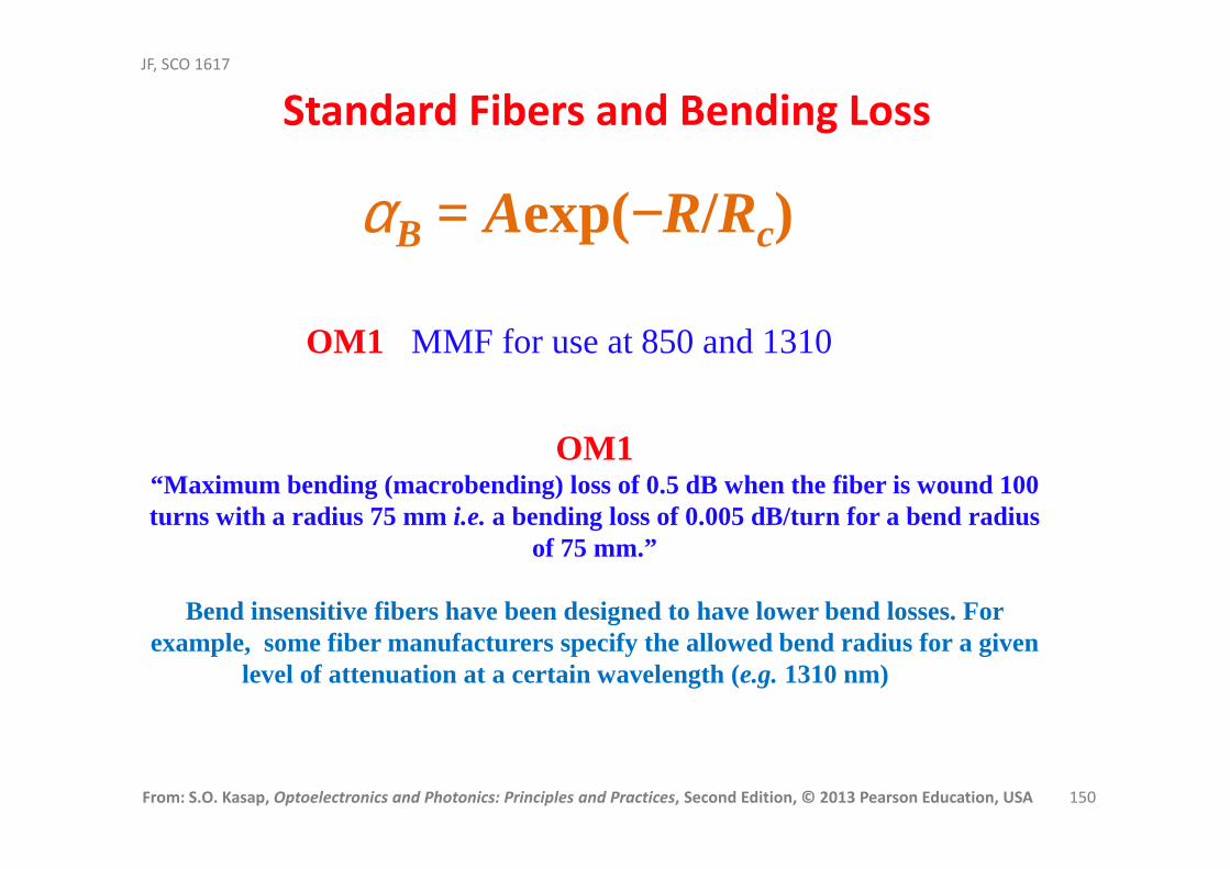
Standard Fibers and Bending Loss
αB = Aexp(−R/Rc)
OM1 MMF for use at 850 and 1310
OM1 “Maximum bending (macrobending) loss of 0.5 dB when the fiber is wound 100 turns with a radius 75 mm i.e.a bending loss of 0.005 dB/turn for a bend radius
of 75 mm.”
Bend insensitive fibers have been designed to have lower bend losses. For example, some fiber manufacturers specify the allowed bend radius for a given
level of attenuation at a certain wavelength (e.g.1310 nm)

From: S.O. Kasap, Optoelectronics and Photonics: Principles and Practices, Second Edition, © 2013 Pearson Education, USA 151
JF, SCO 1617
Example: Experiments on a standard SMF operating around 1550 nm have shown that thebending loss is 0.124 dB/turn when the bend radius is 12.5 mm and 15.0 dB/turn when the bendradius is 5.0 mm. What is the loss at a bend radius of 10 mm?
Bending Loss Example
SolutionApply
αB = Aexp(−R/Rc)0.124 dB/turn = Aexp[−(12.5 mm)/Rc]15.0 dB/turn = Aexp[−(5.0 mm)/Rc]
Solve for A and Rc. Dividing the first by the second and separating out Rc we find,
Rc = (12.5 mm − 5.0 mm) / ln(15.0/0.124) = 1.56 mmand A = (15.0 dB/turn) exp[(5.0 mm)/(1.56 mm] = 370 dB/turn
At R = 10 mmαB = Aexp(−R/Rc) = (370)exp[−(10 mm)/(1.56 mm)]
= 0.61 dB/turn.The experimental value is also 0.61 dB/turn to within two decimals.
From: S.O. Kasap, Optoelectronics and Photonics: Principles and Practices, Second Edition, © 2013 Pearson Education, USA 152
JF, SCO 1617
From: S.O. Kasap, Optoelectronics and Photonics: Principles and Practices, Second Edition, © 2013 Pearson Education, USA 152
JF, SCO 1617
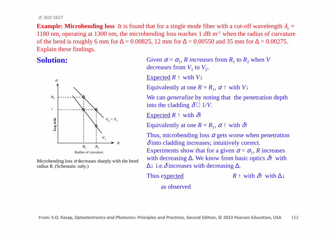
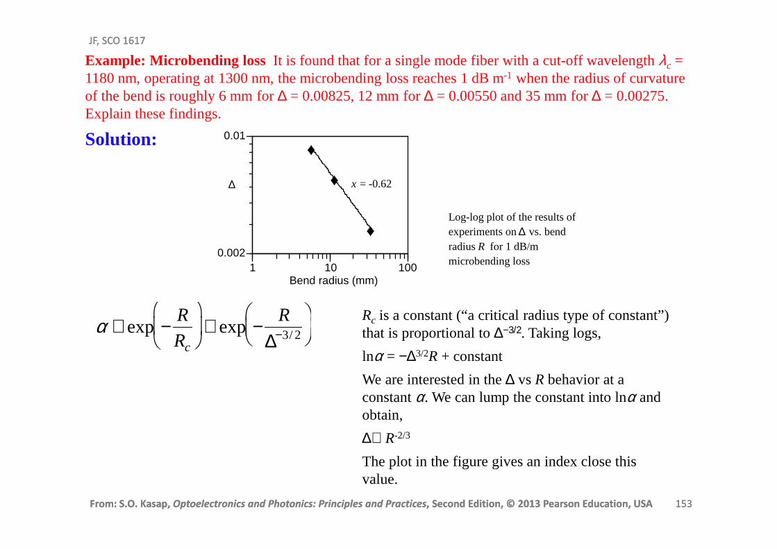
Example: Microbending loss It is found that for a single mode fiber with a cut-off wavelength λc = 1180 nm, operating at 1300 nm, the microbending loss reaches 1 dB m-1 when the radius of curvature of the bend is roughly 6 mm for ∆ = 0.00825, 12 mm for ∆ = 0.00550 and 35 mm for ∆ = 0.00275. Explain these findings.
Solution:
Radius of curvature
α
V1
V2 < V1
R
α1
α2
R1 R2
Microbending loss α decreases sharply with the bendradius R. (Schematic only.)
Given α = α1, R increasesfrom R1 to R2 when Vdecreasesfrom V1 to V2.
Expected R ↑ with V↓Equivalently at one R = R1, α ↑ with V↓We can generalizeby noting that the penetration depth into the cladding δ ∝ 1/V.
Expected R ↑ with δ↑Equivalently at one R = R1, α ↑ with δ↑Thus, microbending loss α gets worse when penetration δ into cladding increases; intuitively correct. Experiments show that for a given α = α1, R increases with decreasing ∆. We know from basic optics δ↑ with ∆↓ i.e.δ increases with decreasing ∆.
Thus expected R ↑ with δ↑ with ∆↓
as observed
From: S.O. Kasap, Optoelectronics and Photonics: Principles and Practices, Second Edition, © 2013 Pearson Education, USA 153
JF, SCO 1617
From: S.O. Kasap, Optoelectronics and Photonics: Principles and Practices, Second Edition, © 2013 Pearson Education, USA 153
JF, SCO 1617
Example: Microbending loss It is found that for a single mode fiber with a cut-off wavelength λc = 1180 nm, operating at 1300 nm, the microbending loss reaches 1 dB m-1 when the radius of curvature of the bend is roughly 6 mm for ∆ = 0.00825, 12 mm for ∆ = 0.00550 and 35 mm for ∆ = 0.00275. Explain these findings.
Solution:
Log-log plot of the results ofexperiments on ∆ vs. bendradius R for 1 dB/mmicrobending loss
♦
♦
♦0.002
0.01
1 10 100Bend radius (mm)
∆ x = -0.62
α ∝exp − R
Rc
∝exp − R
∆−3/ 2
Rc is a constant (“a critical radius type of constant”) that is proportional to ∆−3/2. Taking logs,
lnα = −∆3/2R + constant
We are interested in the ∆ vs R behavior at a constant α. We can lump the constant into lnα and obtain,
∆∝ R-2/3
The plot in the figure gives an index close this value.

From: S.O. Kasap, Optoelectronics and Photonics: Principles and Practices, Second Edition, © 2013 Pearson Education, USA 154
JF, SCO 1617
From: S.O. Kasap, Optoelectronics and Photonics: Principles and Practices, Second Edition, © 2013 Pearson Education, USA 154
JF, SCO 1617
Manufacture of Optical Fibers
From: S.O. Kasap, Optoelectronics and Photonics: Principles and Practices, Second Edition, © 2013 Pearson Education, USA 155
JF, SCO 1617
From: S.O. Kasap, Optoelectronics and Photonics: Principles and Practices, Second Edition, © 2013 Pearson Education, USA 155
JF, SCO 1617
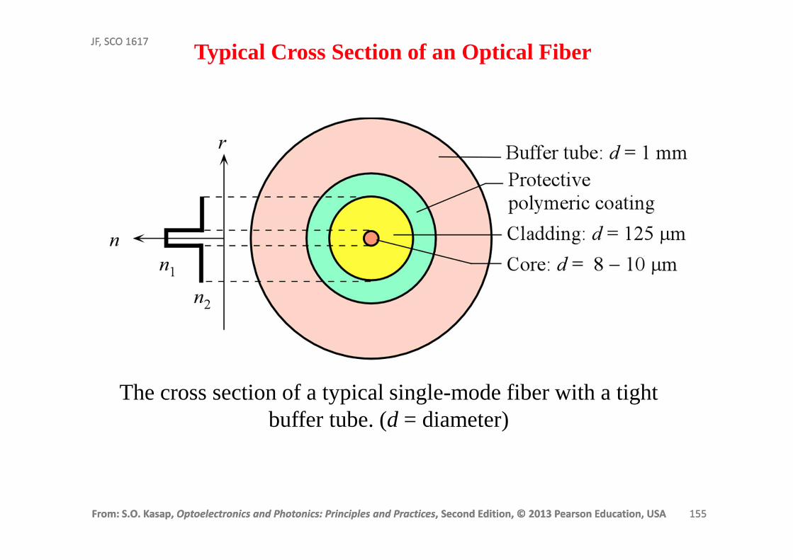
The cross section of a typical single-mode fiber with a tight buffer tube. (d = diameter)
Typical Cross Section of an Optical Fiber

From: S.O. Kasap, Optoelectronics and Photonics: Principles and Practices, Second Edition, © 2013 Pearson Education, USA 156
JF, SCO 1617
From: S.O. Kasap, Optoelectronics and Photonics: Principles and Practices, Second Edition, © 2013 Pearson Education, USA 156
JF, SCO 1617
Outside vapor Deposition (OVD)
Main reactions are
Silicon tetrachloride and oxygen produces silica
SiCl4(gas) + O2(gas) → SiO2(solid) + 2Cl2(gas)
Germanium tetrachloride and oxygen produces germania
GeCl4(gas) + O2(gas) → GeO2(solid) + 2Cl2(gas)
From: S.O. Kasap, Optoelectronics and Photonics: Principles and Practices, Second Edition, © 2013 Pearson Education, USA 157
JF, SCO 1617
From: S.O. Kasap, Optoelectronics and Photonics: Principles and Practices, Second Edition, © 2013 Pearson Education, USA 157
JF, SCO 1617
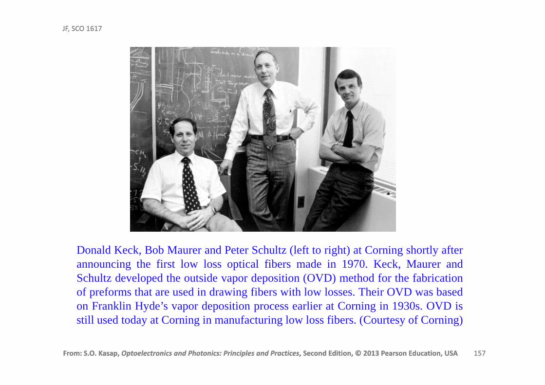
Donald Keck, Bob Maurer and Peter Schultz (left to right) at Corning shortly afterannouncing the first low loss optical fibers made in 1970. Keck, Maurer andSchultz developed the outside vapor deposition (OVD) method for the fabricationof preforms that are used in drawing fibers with low losses. Their OVD was basedon Franklin Hyde’s vapor deposition process earlier at Corning in 1930s. OVD isstill used today at Corning in manufacturing low loss fibers. (Courtesy of Corning)

From: S.O. Kasap, Optoelectronics and Photonics: Principles and Practices, Second Edition, © 2013 Pearson Education, USA 158
JF, SCO 1617
From: S.O. Kasap, Optoelectronics and Photonics: Principles and Practices, Second Edition, © 2013 Pearson Education, USA 158
JF, SCO 1617
Peter Schultz making a germania-doped multimode fiber preform using the outside vapor deposition (OVD) process circa 1972 at Corning. Soot is deposited layer by layer on a thin bait rod rotating and translating in fron t of the flame hydrolysis burner. The first fibers made by the OVD at that time had an attenuation of 4 dB/km, which was among the lowest, and below what Charles Kao thought was needed for optical fiber communications, 20 dB/km (Courtesy of Peter Schultz.)
From: S.O. Kasap, Optoelectronics and Photonics: Principles and Practices, Second Edition, © 2013 Pearson Education, USA 159
JF, SCO 1617
From: S.O. Kasap, Optoelectronics and Photonics: Principles and Practices, Second Edition, © 2013 Pearson Education, USA 159
JF, SCO 1617
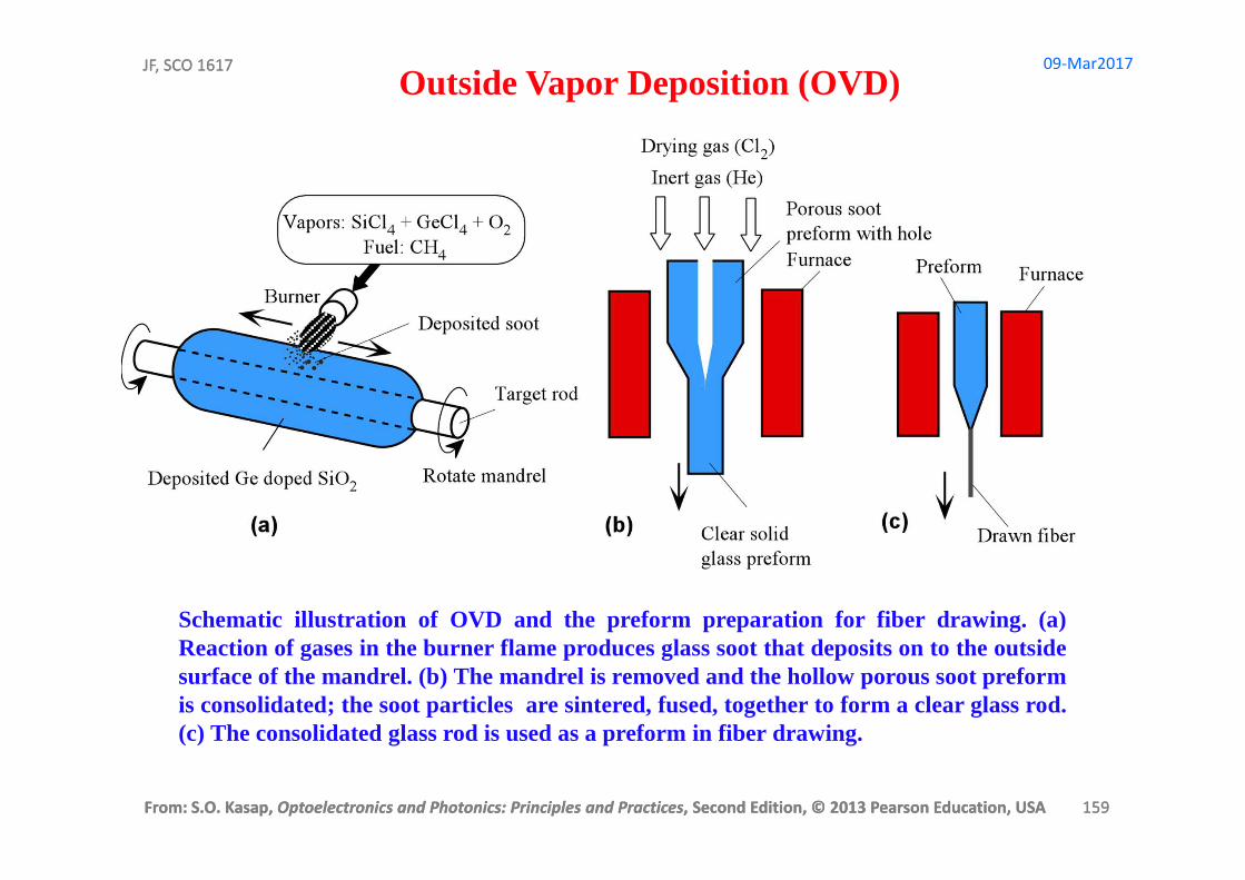
Outside Vapor Deposition (OVD)
Schematic illustration of OVD and the preform preparation for fiber drawing. (a)Reaction of gases in the burner flame produces glass soot that deposits on to the outsidesurface of the mandrel. (b) The mandrel is removed and the hollow porous soot preformis consolidated; the soot particles are sintered, fused, together to form a clear glass rod.(c) The consolidated glass rod is used as a preform in fiber drawing.
09-Mar2017

From: S.O. Kasap, Optoelectronics and Photonics: Principles and Practices, Second Edition, © 2013 Pearson Education, USA 160
JF, SCO 1617
From: S.O. Kasap, Optoelectronics and Photonics: Principles and Practices, Second Edition, © 2013 Pearson Education, USA 160
JF, SCO 1617
Chapter 2 Dielectric Waveguides and Optical Fibers
Charles Kao, Nobel Laureate (2009)Courtesy of the Chinese University of Hong Kong
O material que se segue até ao final deste documento não foi lecionado
nesta aula, embora recomende vivamente a sua visualização.
Sempre se afigure necessário faremos a respetiva análise.
S.O. Kasap, Optoelectronics and Photonics: Principles and Practices, Second Edition, © 2013 Pearson Education© 2013 Pearson Education, Inc., Upper Saddle River, NJ. All rights reserved. This publication is prote cted by Copyright and written permission should be obtained from the
publisher prior to any prohibited reproduction, sto rage in a retrieval system, or transmission in any form or by any means, electronic, mechanical, photo copying, recording, or likewise. For information regarding permission(s), write to: Rights and Permissions Department, Pearso n Education, Inc., Upper Saddle River, NJ 07458.
09-Mar2017

From: S.O. Kasap, Optoelectronics and Photonics: Principles and Practices, Second Edition, © 2013 Pearson Education, USA 161
JF, SCO 1617WAVELENGTH DIVISION MULTIPLEXING: WDM
From: S.O. Kasap, Optoelectronics and Photonics: Principles and Practices, Second Edition, © 2013 Pearson Education, USA 162
JF, SCO 1617
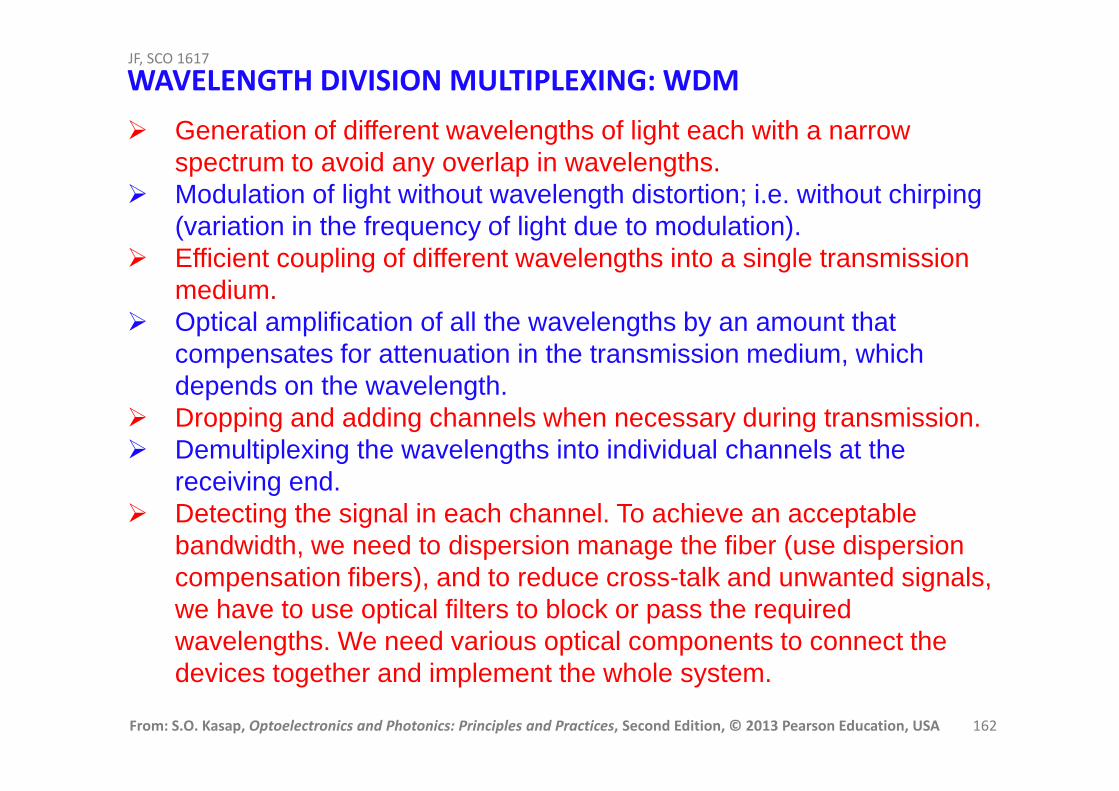
WAVELENGTH DIVISION MULTIPLEXING: WDM
Generation of different wavelengths of light each with a narrow spectrum to avoid any overlap in wavelengths.
Modulation of light without wavelength distortion; i.e. without chirping(variation in the frequency of light due to modulation).
Efficient coupling of different wavelengths into a single transmission medium.
Optical amplification of all the wavelengths by an amount that compensates for attenuation in the transmission medium, which depends on the wavelength.
Dropping and adding channels when necessary during transmission. Demultiplexing the wavelengths into individual channels at the
receiving end. Detecting the signal in each channel. To achieve an acceptable
bandwidth, we need to dispersion manage the fiber (use dispersion compensation fibers), and to reduce cross-talk and unwanted signals, we have to use optical filters to block or pass the required wavelengths. We need various optical components to connect the devices together and implement the whole system.
From: S.O. Kasap, Optoelectronics and Photonics: Principles and Practices, Second Edition, © 2013 Pearson Education, USA 163
JF, SCO 1617
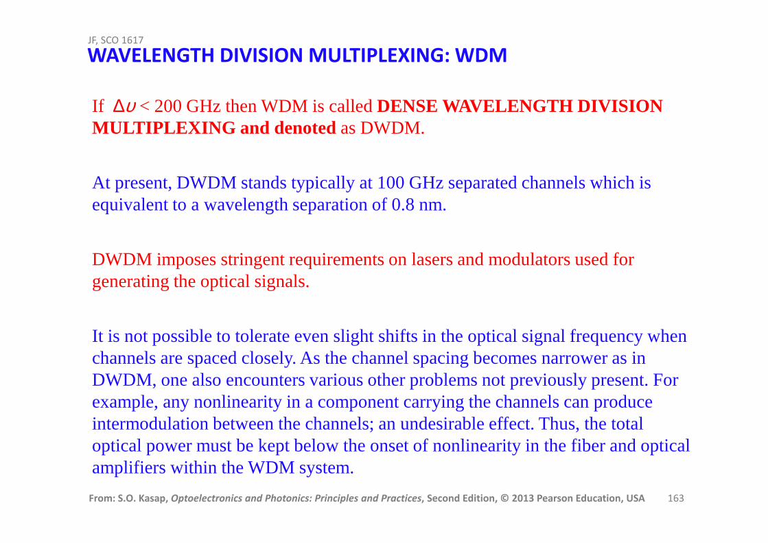
WAVELENGTH DIVISION MULTIPLEXING: WDM
If ∆υ < 200 GHz then WDM is called DENSE WAVELENGTH DIVISION MULTIPLEXING and denoted as DWDM.
At present, DWDM stands typically at 100 GHz separated channels which is equivalent to a wavelength separation of 0.8 nm.
DWDM imposes stringent requirements on lasers and modulators used for generating the optical signals.
It is not possible to tolerate even slight shifts in the optical signal frequency when channels are spaced closely. As the channel spacing becomes narrower as in DWDM, one also encounters various other problems not previously present. For example, any nonlinearity in a component carrying the channels can produce intermodulation between the channels; an undesirable effect. Thus, the total optical power must be kept below the onset of nonlinearity in the fiber and optical amplifiers within the WDM system.
From: S.O. Kasap, Optoelectronics and Photonics: Principles and Practices, Second Edition, © 2013 Pearson Education, USA 164
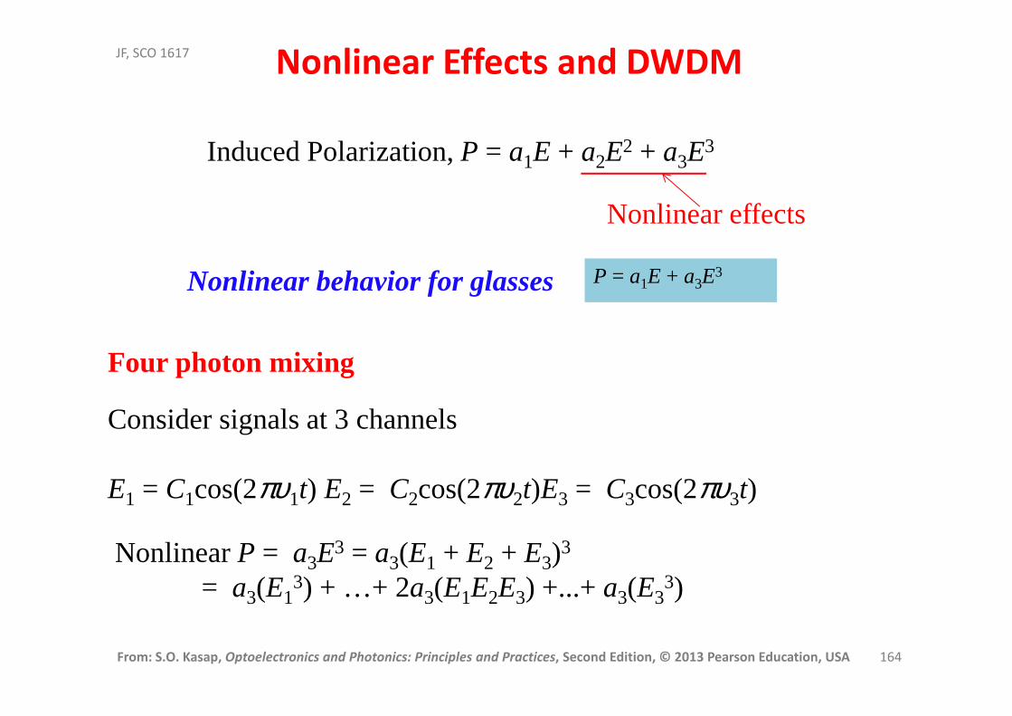
JF, SCO 1617 Nonlinear Effects and DWDM
Induced Polarization, P = a1E + a2E2 + a3E3
P = a1E + a3E3Nonlinear behavior for glasses
Nonlinear effects
Consider signals at 3 channels
E1 = C1cos(2πυ1t) E2 = C2cos(2πυ2t)E3 = C3cos(2πυ3t)
NonlinearP = a3E3 = a3(E1 + E2 + E3)3
= a3(E13) + …+ 2a3(E1E2E3) +...+a3(E3
3)
Four photon mixing

From: S.O. Kasap, Optoelectronics and Photonics: Principles and Practices, Second Edition, © 2013 Pearson Education, USA 165
JF, SCO 1617 Nonlinear Effects and DWDM
NonlinearP = a3(E13) +…+ 2a3(E1E2E3) +...+a3(E3
3)
NonlinearP = …+ 2a3C1C2C3cos(2πυ1t)cos(2πυ2t)cos(2πυ3t) +…
Frequencies mix and can be written as sum and difference
frequencies
Consider three optical signals atυ1
υ2 = (υ1 + 100 GHz )
υ3 = (υ2 + 100 GHz ) = (υ1 + 200 GHz)

From: S.O. Kasap, Optoelectronics and Photonics: Principles and Practices, Second Edition, © 2013 Pearson Education, USA 166
JF, SCO 1617
Nonlinear Effects and DWDM
Four Photon (Wave) Mixing
Three photons (υ1, υ2, υ3 ) mix to generate a fourth photon (υ4 )
υ4 = υ1 + υ2 − υ3
υ4 = υ1 + ( υ1 + 100 GHz ) − (υ1 + 200 GHz)
υ4 = υ1 − 100 GHz on top of previous channel

From: S.O. Kasap, Optoelectronics and Photonics: Principles and Practices, Second Edition, © 2013 Pearson Education, USA 167
JF, SCO 1617
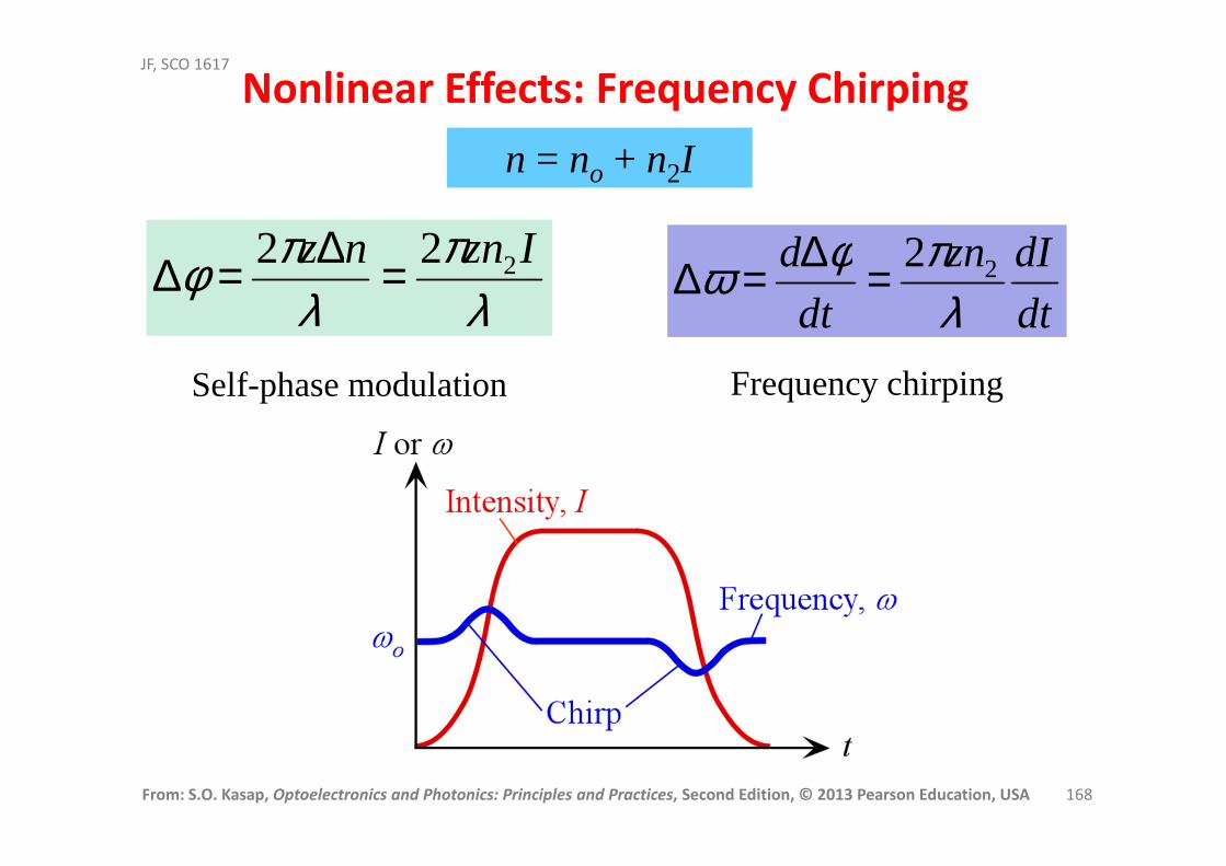
Nonlinear Effects: Frequency Chirping
2312 11 Eaa
E
Pn
ooor
+
+=+==
εεεε
n = no + n2I
Nonlinear refractive index
λπ
λπφ Iznnz 222 =∆=∆
dt
dIzn
dt
d
λπφω 22=∆=∆
Self-phase modulation Frequency chirping
From: S.O. Kasap, Optoelectronics and Photonics: Principles and Practices, Second Edition, © 2013 Pearson Education, USA 168
JF, SCO 1617
Nonlinear Effects: Frequency Chirping
n = no + n2I
λπ
λπφ Iznnz 222 =∆=∆
dt
dIzn
dt
d
λπφω 22=∆=∆
Self-phase modulation Frequency chirping

From: S.O. Kasap, Optoelectronics and Photonics: Principles and Practices, Second Edition, © 2013 Pearson Education, USA 169
JF, SCO 1617
Stimulated Brillouin Scattering
(a) Scattering of a forward travelling EM wave A by an acoustic wave results in a reflected, backscattered, wave B that has a slightly different frequency, by Ω. (b) The forward and
reflected waves, A and B respectively, interfere to give rise to a standing wave that propagates at the acoustic velocity va. As a result of electrostriction, an acoustic wave is
generated that reinforces the original acoustic wave and stimulates further scattering.
From: S.O. Kasap, Optoelectronics and Photonics: Principles and Practices, Second Edition, © 2013 Pearson Education, USA 170
JF, SCO 1617
Stimulated Brillouin Scattering (SBS)
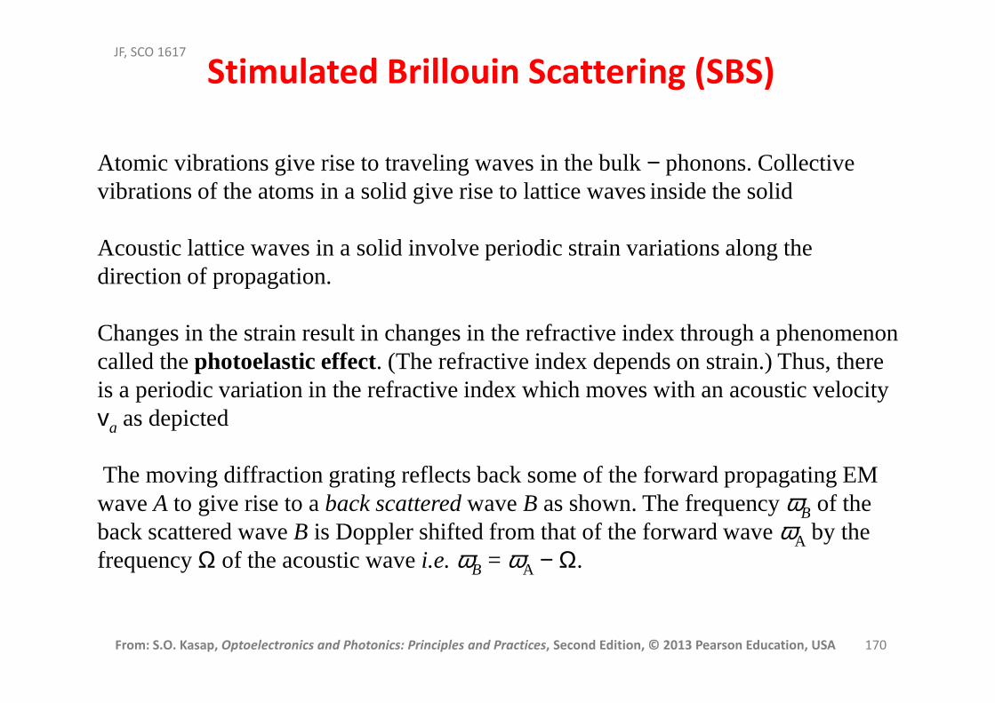
Atomic vibrations give rise to traveling waves in the bulk − phonons. Collective vibrations of the atoms in a solid give rise to lattice waves inside the solid
Acoustic lattice waves in a solid involve periodic strain variations along the direction of propagation.
Changes in the strain result in changes in the refractive index through a phenomenon called the photoelastic effect. (The refractive index depends on strain.) Thus, there is a periodic variation in the refractive index which moves with an acoustic velocity va as depicted
The moving diffraction grating reflects back some of the forward propagating EM wave A to give rise to aback scatteredwave B as shown. The frequency ωB of the back scattered wave B is Doppler shifted from that of the forward wave ωA by the frequency Ω of the acoustic wave i.e. ωB = ωA − Ω.
From: S.O. Kasap, Optoelectronics and Photonics: Principles and Practices, Second Edition, © 2013 Pearson Education, USA 171
JF, SCO 1617
Stimulated Brillouin Scattering (SBS)
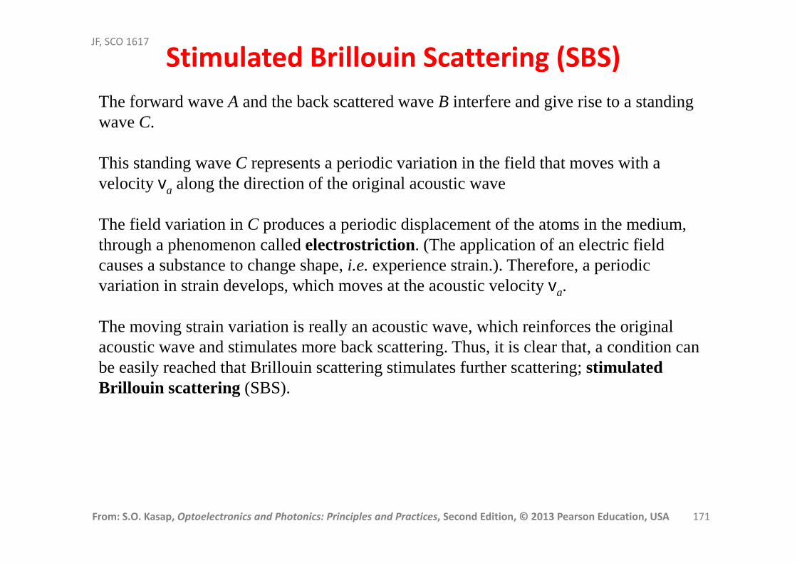
The forward wave A and the back scattered wave B interfere and give rise to a standing wave C.
This standing wave C represents a periodic variation in the field that moves with a velocity va along the direction of the original acoustic wave
The field variation in C produces a periodic displacement of the atoms in the medium, through a phenomenon called electrostriction. (The application of an electric field causes a substance to change shape, i.e.experience strain.). Therefore, a periodic variation in strain develops, which moves at the acoustic velocity va.
The moving strain variation is really an acoustic wave, which reinforces the original acoustic wave and stimulates more back scattering. Thus, it is clear that, a condition can be easily reached that Brillouin scattering stimulates further scattering; stimulated Brillouin scattering (SBS).

From: S.O. Kasap, Optoelectronics and Photonics: Principles and Practices, Second Edition, © 2013 Pearson Education, USA 172
JF, SCO 1617
Stimulated Brillouin Scattering (SBS)
The SBS effect increases as the input light power increase
The SBS effect increases as the spectral width of the input light becomes narrower.
The onset of SBS depends not only on the fiber type and core diameter, but also on the spectral width ∆λ of the laser output spectrum.
SBS is enhanced as the laser spectral width ∆λ is narrowed or the duration of light pulse is lengthened.
Typical values: For a directly modulated laser diode emitting at 1550 nm into a single mode fiber, the onset of SBS is expected to occur at power levels greater than 20 − 30 mW. In DWDM systems with externally modulated lasers, i.e. narrower ∆λ, the onset of SBS can be as low as ~10 mW. SBS is an important limiting factor in transmitting high power signals in WDM systems.

From: S.O. Kasap, Optoelectronics and Photonics: Principles and Practices, Second Edition, © 2013 Pearson Education, USA 173
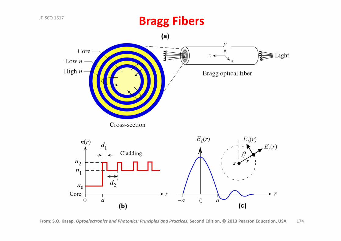
JF, SCO 1617 Bragg Fibers
The high (n1) and low (n2) alternating refractive index profile constitutes a Bragg grating which acts as a dielectric mirror.
There is a band of wavelengths, forming a stop-band, that are not allowed to propagate into the Bragg grating.
We can also view the periodic variation in n as forming a photonic crystal cladding in one-dimension, along the radial direction, with a stop-band, i.e. a photonic bandgap.
Light is bound within the core of the guide for wavelengths within this stop-band. Light can only propagate along z.
d1 = λ/n1 and d2 = λ/n2
Bragg fibers have a core region surrounded by a cladding that is made up of concentrating layers of high low refractive index dielectric media
The core can be a low refractive index solid material or simply hollow. In the latter case, we have a hollow Bragg fiber.
∴ d1n1 = d2n2
From: S.O. Kasap, Optoelectronics and Photonics: Principles and Practices, Second Edition, © 2013 Pearson Education, USA 174
JF, SCO 1617 Bragg Fibers
From: S.O. Kasap, Optoelectronics and Photonics: Principles and Practices, Second Edition, © 2013 Pearson Education, USA 175
JF, SCO 1617 Bragg Fibers
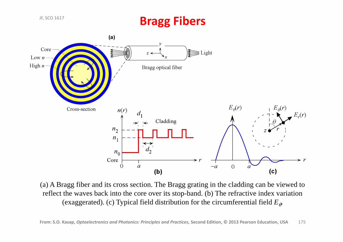
(a) A Bragg fiber and its cross section. The Bragg grating in the cladding can be viewed to reflect the waves back into the core over its stop-band. (b) The refractive index variation
(exaggerated). (c) Typical field distribution for the circumferential field Eθ.

From: S.O. Kasap, Optoelectronics and Photonics: Principles and Practices, Second Edition, © 2013 Pearson Education, USA 176
JF, SCO 1617 Photonic Crystal Fibers: Holey Fibers
(a) A solid core PCF. Light is index guided. The cladding has a hexagonal array of
holes. d is the hole diameter and Λ is the array pitch, spacing between the
holes (b) and (c) A hollow core PCF. Light is photonic bandgap (PBG) guided.
From: S.O. Kasap, Optoelectronics and Photonics: Principles and Practices, Second Edition, © 2013 Pearson Education, USA 177
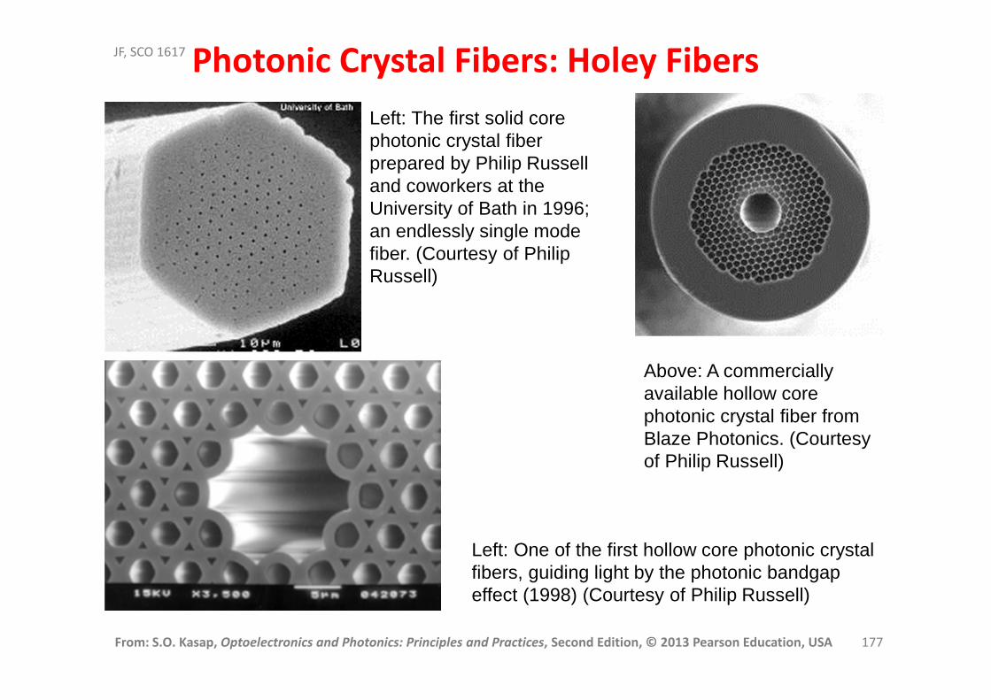
JF, SCO 1617 Photonic Crystal Fibers: Holey Fibers
Left: The first solid core photonic crystal fiber prepared by Philip Russell and coworkers at the University of Bath in 1996; an endlessly single mode fiber. (Courtesy of Philip Russell)
Left: One of the first hollow core photonic crystal fibers, guiding light by the photonic bandgap effect (1998) (Courtesy of Philip Russell)
Above: A commercially available hollow core photonic crystal fiber from Blaze Photonics. (Courtesy of Philip Russell)
From: S.O. Kasap, Optoelectronics and Photonics: Principles and Practices, Second Edition, © 2013 Pearson Education, USA 178
JF, SCO 1617
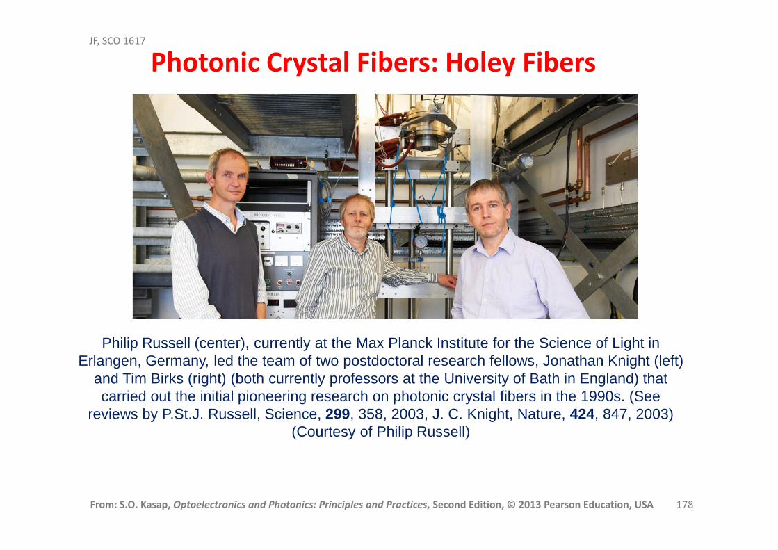
Photonic Crystal Fibers: Holey Fibers
Philip Russell (center), currently at the Max Planck Institute for the Science of Light in Erlangen, Germany, led the team of two postdoctoral research fellows, Jonathan Knight (left)
and Tim Birks (right) (both currently professors at the University of Bath in England) that carried out the initial pioneering research on photonic crystal fibers in the 1990s. (See
reviews by P.St.J. Russell, Science, 299, 358, 2003, J. C. Knight, Nature, 424, 847, 2003) (Courtesy of Philip Russell)
From: S.O. Kasap, Optoelectronics and Photonics: Principles and Practices, Second Edition, © 2013 Pearson Education, USA 179
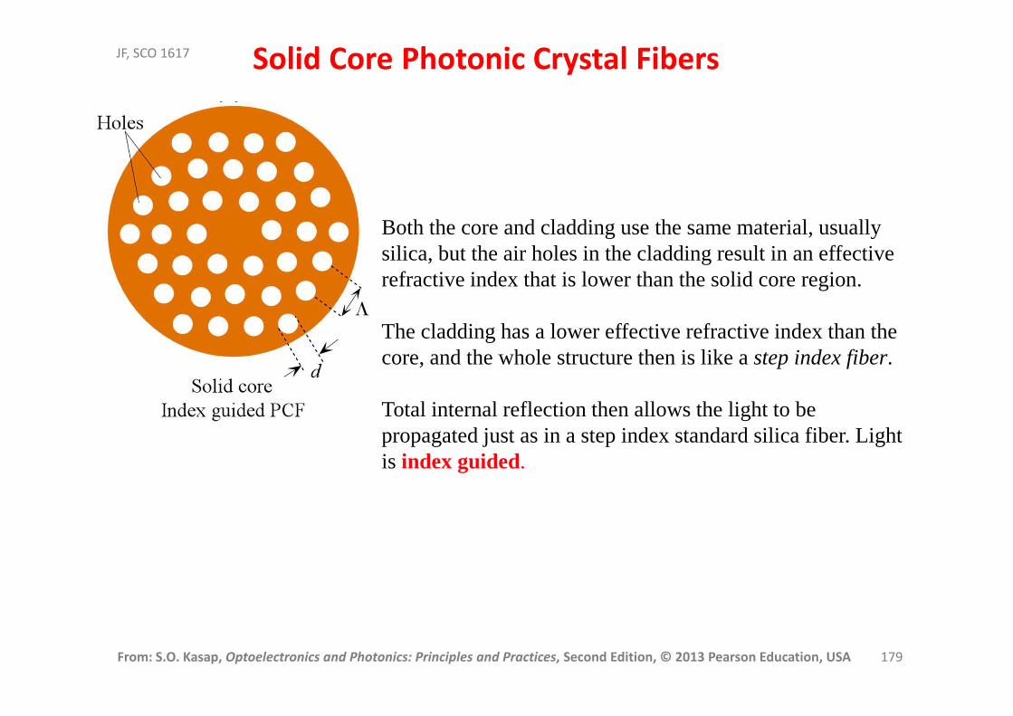
JF, SCO 1617 Solid Core Photonic Crystal Fibers
Both the core and cladding use the same material, usually silica, but the air holes in the cladding result in an effective refractive index that is lower than the solid core region.
The cladding has a lower effective refractive index than the core, and the whole structure then is like a step index fiber.
Total internal reflection then allows the light to be propagated just as in a step index standard silica fiber. Light is index guided.

From: S.O. Kasap, Optoelectronics and Photonics: Principles and Practices, Second Edition, © 2013 Pearson Education, USA 180
JF, SCO 1617 Solid Core Photonic Crystal Fibers
The solid can be pure silica, rather than germania-doped silica, and hence exhibits lower scattering loss.
Single mode propagation can occur over a very large range of wavelengths, almost as if the fiber is endlessly single mode(ESM). The reason is that the PC in the cladding acts as a filter in the transverse direction, which allows the higher modes to escape (leak out) but not the fundamental mode.
(a) The fundamental mode is confined. (b) Higher modes have more nodes and can leak away through the space.

From: S.O. Kasap, Optoelectronics and Photonics: Principles and Practices, Second Edition, © 2013 Pearson Education, USA 181
JF, SCO 1617 Solid Core Photonic Crystal Fibers
ESM operation: The core of a PCF can be made quite large without losing the single mode operation. The refractive index difference can also be made large by having holes in the cladding. Consequently, PCFs can have high numerical apertures and large core areas; thus, more light can be launched into a PCF. Further, the manipulation of the shape and size of the hole, and the type of lattice (and hence the periodicity i.e. the lattice pitch) leads to a much greater control of chromatic dispersion.
(a) The fundamental mode is confined. (b) Higher modes have more nodes and can leak away through the space.
From: S.O. Kasap, Optoelectronics and Photonics: Principles and Practices, Second Edition, © 2013 Pearson Education, USA 182
JF, SCO 1617Hollow Core Photonic Crystal Fibers: Holey Fibers
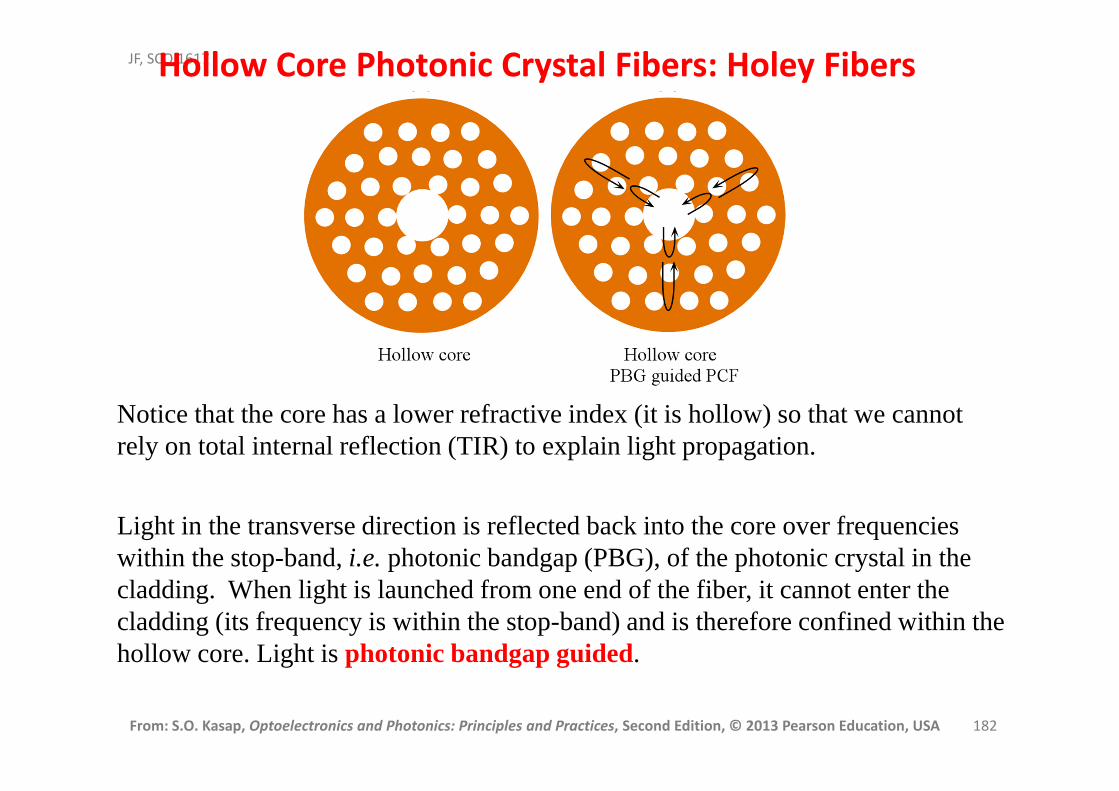
Notice that the core has a lower refractive index (it is hollow) so that we cannot rely on total internal reflection (TIR) to explain light propagation.
Light in the transverse direction is reflected back into the core over frequencies within the stop-band, i.e. photonic bandgap (PBG), of the photonic crystal in the cladding. When light is launched from one end of the fiber, it cannot enter the cladding (its frequency is within the stop-band) and is therefore confined within the hollow core. Light is photonic bandgap guided.

From: S.O. Kasap, Optoelectronics and Photonics: Principles and Practices, Second Edition, © 2013 Pearson Education, USA 183
JF, SCO 1617Hollow Core Photonic Crystal Fibers: Holey Fibers
As recalled by Philip Russell:
"My idea, then, was to trap light in a hollow core by means of a 2D photonic crystal of microscopic air capillaries running along the entire length of a glass fiber. Appropriately designed, this array would support a PBG for incidence from air, preventing the escape of light from a hollow core into the photonic-crystal cladding and avoiding the need for TIR." (P. St.J. Russell, J. Light Wave Technol, 24, 4729, 2006)
The periodic arrangement of the air holes in the cladding creates a photonic bandgap in the transverse direction that confines the light to the hollow core.

From: S.O. Kasap, Optoelectronics and Photonics: Principles and Practices, Second Edition, © 2013 Pearson Education, USA 184
JF, SCO 1617Hollow Core Photonic Crystal Fibers: Holey Fibers
There are certain distinct advantages
Material dispersion is absent.
The attenuation in principle should be potentially very small since there is no Rayleigh scattering in the core. However, scattering from irregularities in the air-cladding interface, that is, surface roughness, seems to limit the attenuation.
High powers of light can be launched without having nonlinear effects such as stimulated Brillouin scattering limiting the propagation.
There are other distinct advantages that are related to strong nonlinear effects, which are associated with the photonic crystal cladding.
From: S.O. Kasap, Optoelectronics and Photonics: Principles and Practices, Second Edition, © 2013 Pearson Education, USA 185
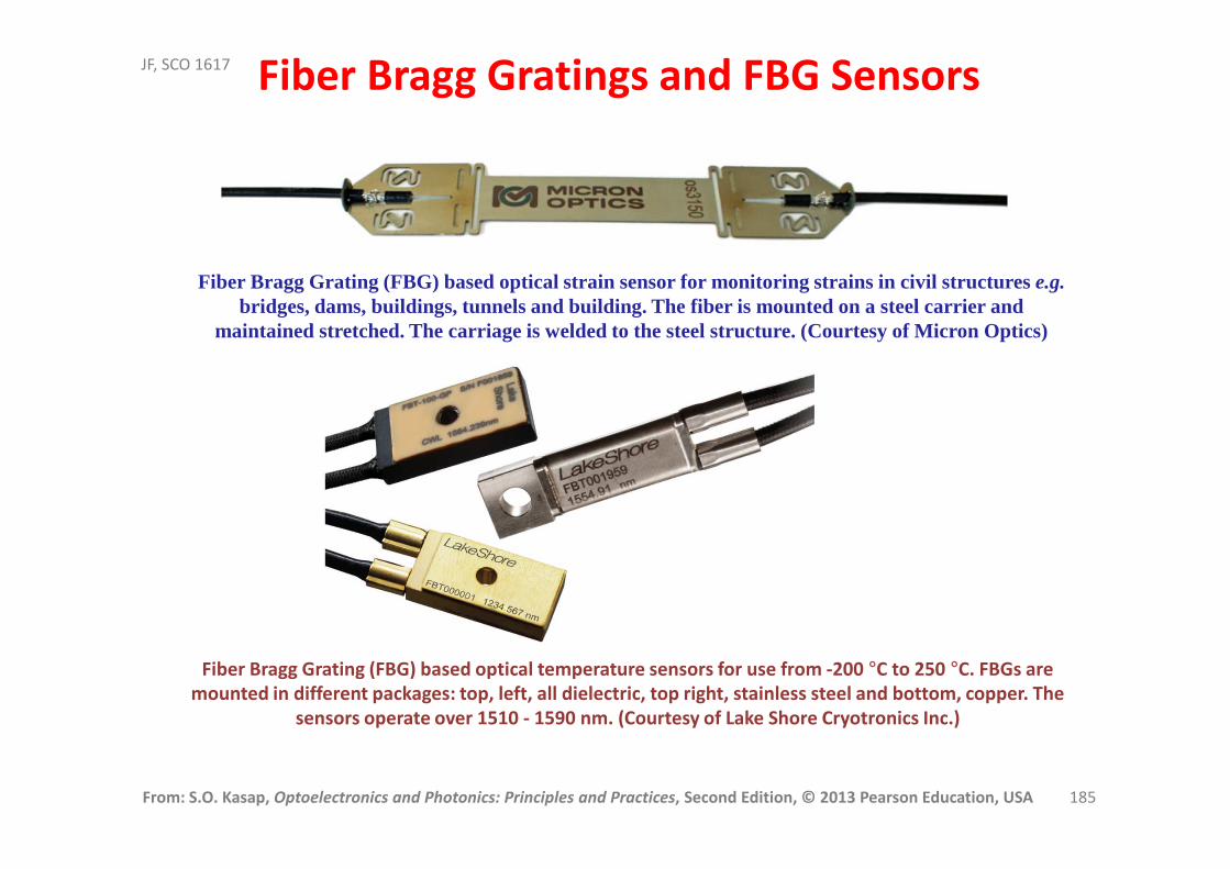
JF, SCO 1617 Fiber Bragg Gratings and FBG Sensors
Fiber Bragg Grating (FBG) based optical strain sensor for monitoring strains in civil structures e.g.bridges, dams, buildings, tunnels and building. The fiber is mounted on a steel carrier and
maintained stretched. The carriage is welded to the steel structure. (Courtesy of Micron Optics)
Fiber Bragg Grating (FBG) based optical temperature sensors for use from -200 °C to 250 °C. FBGs are
mounted in different packages: top, left, all dielectric, top right, stainless steel and bottom, copper. The
sensors operate over 1510 - 1590 nm. (Courtesy of Lake Shore Cryotronics Inc.)

From: S.O. Kasap, Optoelectronics and Photonics: Principles and Practices, Second Edition, © 2013 Pearson Education, USA 186
JF, SCO 1617
FBG: Fiber Bragg Grating
Fiber Bragg grating has a Bragg grating written in the core ofa singlemode fiber over a certain length of the fiber. The Bragg grating reflects anylight that has the Bragg wavelengthλB, which depends on the refractiveindex and the periodicity. The transmitted spectrum has theBraggwavelength missing.

From: S.O. Kasap, Optoelectronics and Photonics: Principles and Practices, Second Edition, © 2013 Pearson Education, USA 187
JF, SCO 1617
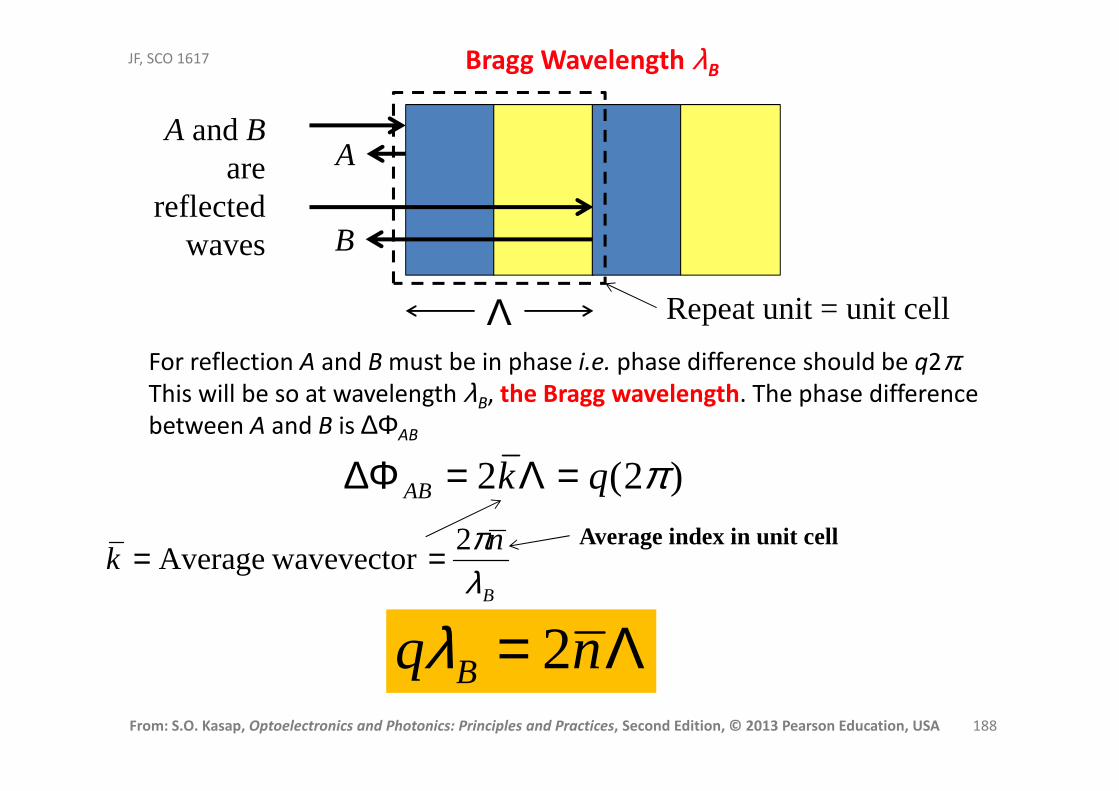
Fiber Bragg Grating: FBG
Variation in n in the grating acts like a dielectric mirrorPartial Fresnel reflections from the changes in the refractive index add in phase
and give rise to a back reflected (back diffracted) wave only at a certain wavelength λB, called the Bragg wavelength
Λ= nq B 2λ
Integer, 1,2,… normally q = 1 is used, the fundamental
From: S.O. Kasap, Optoelectronics and Photonics: Principles and Practices, Second Edition, © 2013 Pearson Education, USA 188
JF, SCO 1617 Bragg Wavelength λB
)2(2 πqkAB =Λ=∆Φ
A
B
Λ Repeat unit = unit cell
For reflection A and B must be in phase i.e. phase difference should be q2π.
This will be so at wavelength λB, the Bragg wavelength. The phase difference
between A and B is ∆ΦAB
A and Bare
reflected waves
B
nk
λπ2
wavevectorAverage ==Average index in unit cell
Λ= nq B 2λ
From: S.O. Kasap, Optoelectronics and Photonics: Principles and Practices, Second Edition, © 2013 Pearson Education, USA 189
JF, SCO 1617
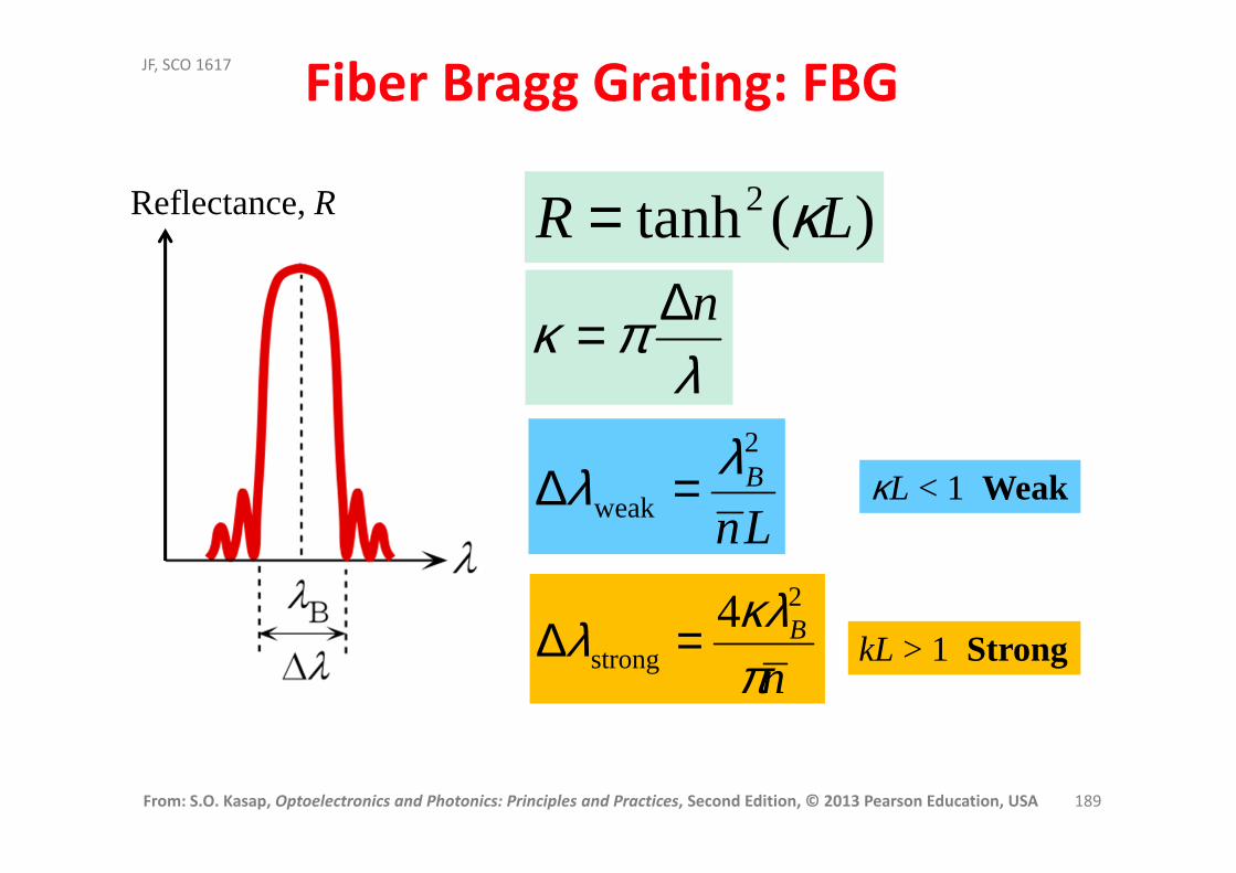
Fiber Bragg Grating: FBG
)(tanh2 LR κ=
λπκ n∆=
LnB2
weak
λλ =∆
nB
πκλλ
2
strong
4=∆
κL < 1 Weak
kL > 1 Strong
Reflectance, R

From: S.O. Kasap, Optoelectronics and Photonics: Principles and Practices, Second Edition, © 2013 Pearson Education, USA 190
JF, SCO 1617
FBG Sensors
Λ+Λ= δδδλ nnB 22
TLB
B δααλ
δλ)( TCRI +=
εδ epnn 321−=
Photoelastic or elasto-optic coefficient
Strain

From: S.O. Kasap, Optoelectronics and Photonics: Principles and Practices, Second Edition, © 2013 Pearson Education, USA 191
JF, SCO 1617
FBG Sensors
Λ+Λ= δδδλ nnB 22

From: S.O. Kasap, Optoelectronics and Photonics: Principles and Practices, Second Edition, © 2013 Pearson Education, USA 192
JF, SCO 1617
FBG Sensors
A highly simplified schematic diagram of a multiplexed Bragg grating based sensing system. The FBG sensors are distributed on a single fiber that is embedded in the structure in which strains are
to be monitored. The coupler allows optical power to be coupled from one fiber to the other.
From: S.O. Kasap, Optoelectronics and Photonics: Principles and Practices, Second Edition, © 2013 Pearson Education, USA 193
JF, SCO 1617
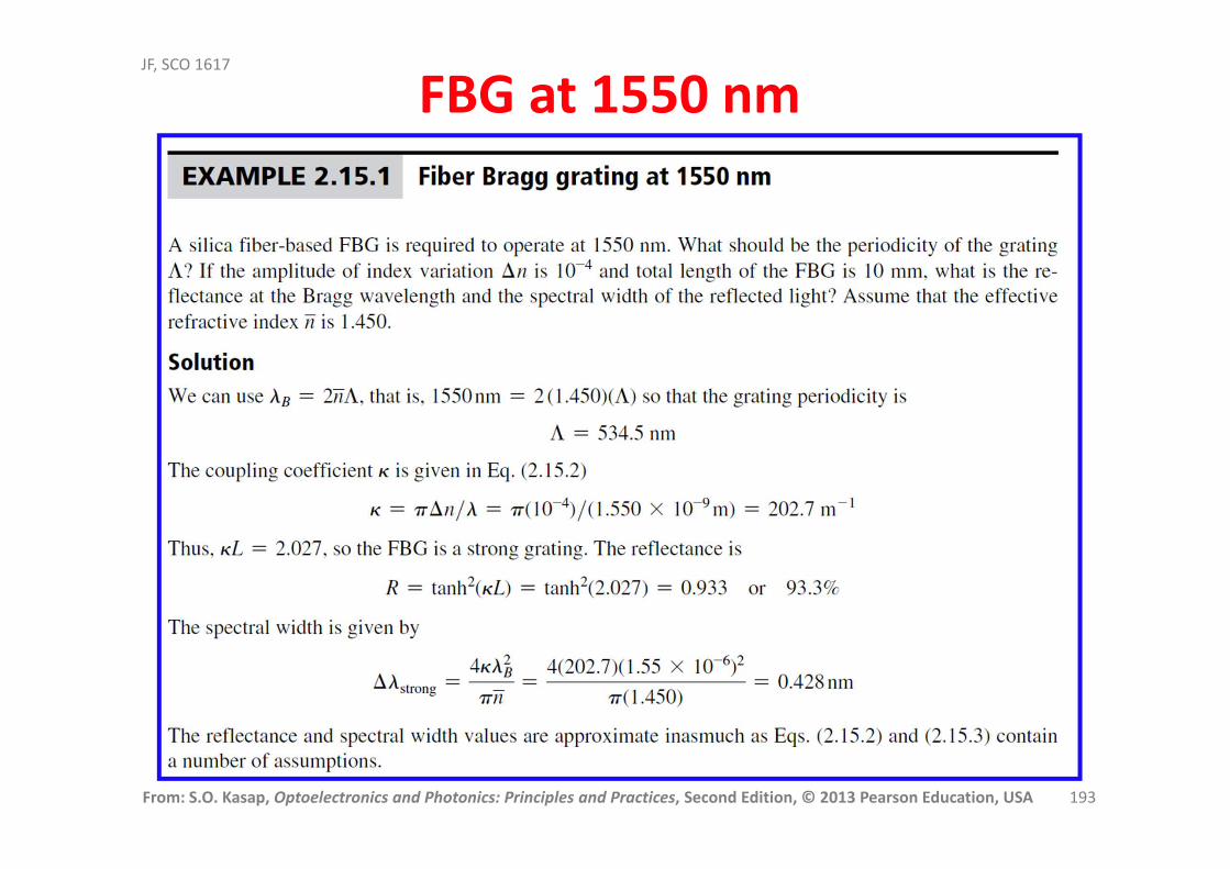
FBG at 1550 nm

From: S.O. Kasap, Optoelectronics and Photonics: Principles and Practices, Second Edition, © 2013 Pearson Education, USA 194
JF, SCO 1617
From: S.O. Kasap, Optoelectronics and Photonics: Principles and Practices, Second Edition, © 2013 Pearson Education, USA 194
JF, SCO 1617
Updates andCorrected Slides
Class Demonstrations
Class Problems
Check author’s websitehttp://optoelectronics.usask.ca
Email errors and corrections to [email protected]


![[S. o. kasap]_principles_of_electronic_materials_a(book_zz.org)](https://img.pdfslide.us/doc/110x75/55a6a6051a28abda2e8b468e/s-o-kasapprinciplesofelectronicmaterialsabookzzorg.jpg)