Embed Size (px)
Citation preview

Appears in the 14th International Conference on Architectural Support for Programming Languages and Operating Systems (ASPLOS’09)
Gordon: Using Flash Memory to Build Fast, Power-efficient Clustersfor Data-intensive Applications
Adrian M. Caulfield Laura M. Grupp Steven SwansonDepartment of Computer Science and Engineering
University of California, San Diego{acaulfie,lgrupp,swanson}@cs.ucsd.edu
AbstractAs our society becomes more information-driven, we havebegun to amass data at an astounding and accelerating rate.At the same time, power concerns have made it difficult tobring the necessary processing power to bear on querying,processing, and understanding this data. We describe Gor-don, a system architecture for data-centric applications thatcombines low-power processors, flash memory, and data-centric programming systems to improve performance fordata-centric applications while reducing power consump-tion. The paper presents an exhaustive analysis of the designspace of Gordon systems, focusing on the trade-offs betweenpower, energy, and performance that Gordon must make. Itanalyzes the impact of flash-storage and the Gordon architec-ture on the performance and power efficiency of data-centricapplications. It also describes a novel flash translation layertailored to data-intensive workloads and large flash storagearrays. Our data show that, using technologies available inthe near future, Gordon systems can out-perform disk-basedclusters by 1.5× and deliver up to 2.5× more performanceper watt.
Categories and Subject Descriptors C.5.5 [Computer Sys-tems Organization]: Computer System Implementation—Servers; C.3 [Computer Systems Organization]: Special-Purpose and Application-Based Systems; C.4 [ComputerSystems Organization]: Performance of Systems
General Terms Performance
Keywords Cluster architecture, data centric, Flash memory,solid-state storage
1. IntroductionWe live in a world overflowing with data. From the hand-held to the data center we are collecting and analyzing ever-greater amounts of information. Companies like Google andMicrosoft routinely process many terabytes of data, andusers of desktop search engines routinely pose queries acrossthe 100s of gigabytes of data stored on their hard drives.There is no reason to expect our appetite for collecting andprocessing data to stop growing at its current breakneckspeed.
Permission to make digital or hard copies of all or part of this work for personal orclassroom use is granted without fee provided that copies are not made or distributedfor profit or commercial advantage and that copies bear this notice and the full citationon the first page. To copy otherwise, to republish, to post on servers or to redistributeto lists, requires prior specific permission and/or a fee.ASPLOS’09, March 7–11, 2009, Washington, DC, USA.Copyright c© 2009 ACM 978-1-60558-215-3/09/03. . . $5.00
To satiate our appetite for large-scale data processingcurrent technology must overcome three challenges. First,the recent slowdown in uni-processor performance and thedifficulties in programming their CMP replacements makesit increasingly difficult to bring large computing power tobear on a single problem. Second, while hard drive capacitycontinues to grow, the latency and bandwidth that hard drivescan deliver do not. Third, power constraints due to cooling,economic, and ecological concerns severely limit the rangeof possible solutions for both of these problems.
On each of these fronts some progress has been made:For data-centric applications, programming models such asMap-Reduce [17] and Dryad [31] largely automate the taskof parallelizing data-processing programs. Solid state stor-age devices offer increased bandwidth and reduced latencyfor mass storage. Finally, processor manufacturers have de-veloped very capable, yet very power-efficient processors.
For data-centric computing, the most fundamental ofthese three advances is the rise of solid-state storage. Flashmemory’s performance characteristics enable systems faroutside the design space covered by existing technolo-gies such as conventional servers, processor-in-disk, andprocessor-in-memory systems. The highest density flashmemories available today (or in the near future) offer 16×the density per package of DRAM at 1/16 the power [9, 36].In the near future, an array of four flash packages will beable to deliver 4× the read bandwidth of a high-end disk at1/30 the power and a fraction of the latency. These advan-tages, combined with the fact that solid state storage arrayscomprise many discrete chips, instead of a few large drives,provide vastly more flexibility in the architecture of a com-bined computing and storage platform.
This paper describes Gordon, a flash-based system archi-tecture for massively parallel, data-centric computing. Gor-don leverages solid-state disks, low-power processors, anddata-centric programming paradigms to deliver enormousgains in performance and power efficiency. In designing andevaluating Gordon, we make the following contributions:
1. A description of the Gordon architecture.2. A flash management software layer that allows highly-
parallel operation of large arrays of flash devices.3. An evaluation of flash management techniques for data-
centric applications.4. A thorough analysis of the Gordon system design space
and the trade-offs between power, energy, and perfor-mance that Gordon must make.
5. A discussion of cost, virtualization, and system-level is-sues in Gordon machines.
Our results show that Gordon systems can deliver up to2.5× the computation per energy of a conventional cluster-
1

Appears in the 14th International Conference on Architectural Support for Programming Languages and Operating Systems (ASPLOS’09)
based system while increasing performance by a factor of upto 1.5. We also demonstrate that our flash management sys-tem can deliver up to 900MB/s of read and write bandwidth.
The rest of this paper is organized as follows. Section 2provides background on the technologies that Gordon uti-lizes. Section 3 describes the architecture of a Gordon sys-tem. Sections 4 and 5 describe Gordon’s flash storage systemand our design space exploration. Section 6 discusses usagemodels for Gordon systems and directions for future work.Section 7 concludes.
2. BackgroundGordon relies on three technologies: large-scale data-parallelprogramming systems, solid-state storage, and low-powerprocessors. Data-centric computing has been a topic of re-search for some time, and we provide a brief overview be-low. Solid-state storage is a more recent development, andthe architectural trade-offs it offers are less well-known, sowe discuss them briefly here and in more depth in Section 4.We discuss the recent advances in commercially availablelow-power processors that Gordon leverages in the next sec-tion.2.1 Peta-scale data-centric parallel programmingIndustrial researchers have recently developed several sys-tems for processing extremely large data sets in parallel. Twoof these systems, Dryad [31] and MapReduce [17], offer analternative to parallel databases [18, 25, 19] for managingand computing with massive data sets. They focus specif-ically on handling large-scale data in enterprise-scale clus-ters composed of commodity hardware. Both systems pro-vide simple abstractions for specifying data-parallel compu-tations and then automate the task of actually making themrun in parallel.
MapReduce, in particular, has received a great deal of re-cent attention. Several implementations are publicly avail-able [1, 38], and researchers have used MapReduce in do-mains ranging from natural language processing [17], to ma-chine learning [16], to scientific computing [35]. Extensionshave also been proposed to enhance and extend its function-ality [15].
MapReduce programs operate on a set of input key-valuepairs. A user-supplied map function takes an input key-valuepair and generates a set of intermediate pairs. The systemgroups the intermediate pairs by key and then applies thereduce function to each group. The reduce function generatesthe final output key-value pairs. MapReduce runs on top of adistributed, reliable file system [24].
Dryad takes a different approach and supports a widerrange of application structures, but increases complexity.Dryad programs are a generalization of UNIX pipes to ar-bitrary directed acyclic graphs of processing steps connectedby uni-directional channels. The system maps the process-ing steps and channels onto available hardware, virtualizingresources as needed.2.2 Solid-state storageFlash memory has risen to prominence over the last decadedue to the growing popularity of mobile devices with largestorage requirements (iPods, digital cameras, etc.). These de-vices make up the vast majority of the NAND flash memorymarket. They do not require particularly high performancebut they do require cheap, high-density, low-power, persis-tent storage. In response to these requirements, flash manu-facturers have primarily pursued density and cost improve-ments and paid less attention to performance. This pressurehas allowed flash density to increase by 85% per year forthe past decade (Figure 1), with 64Gb devices due out nextyear [34, 10].
Despite these gains in density, flash’s full potential forhigh-performance storage is far from realization. While den-sity has improved, other aspects of flash performance havenot kept pace. For instance, the bandwidth on flash devices’8-bit bus (typically 40MB/s) has not increased since 1995.Likewise, the pin-level interface is primitive by modern stan-dards. Industrial efforts [7, 8] are underway to remedy theseproblems and promise to raise peak bus bandwidth to at least133MB/s.
In addition to device advances, system architecture, soft-ware, and management technology for flash memory are ad-vancing as well. Several efforts have sought to improve orrefine flash storage performance in general-purpose systems.These include new chip-level interfaces [39], solid-state diskorganizations [12], improvements in the flash translationlayer that abstracts away flash’s idiosyncrasies [13], andsystem-level interfaces [2].
Taken together, these advances signal the beginning offlash memories’ “coming of age” as a high-performancestorage technology. In the next section we describe a systemarchitecture designed to exploit flash’s unique capabilities.
3. Gordon’s system architectureThe Gordon system architecture uses the technology de-scribed in Section 2 to put terabytes of solid-state storagein close proximity with 100s or 1000s of power-efficientprocessors. The processors communicate over a simple in-terconnect and execute independent instances of a stripped-down operating system along with the software stack neededto implement a data-parallel execution environment likeMapReduce.
The goal of the Gordon design is to reduce the mismatchbetween network bandwidth, disk bandwidth, and CPU per-formance. In a typical high-density cluster (e.g., a rack ofblade servers) a few power-hungry, high-performance pro-cessors provide several GOP/s of computing power, but shareaccess to a small number of (also power-hungry) hard drivesthat provide limited bandwidth. In a Gordon system, the ra-tio of GOP/s to MB/s is quite different: Each processor hasaccess to a flash array that provides enormous bandwidth andvery low latency.
We call the combination of a processor and its flash stor-age system a Gordon node. Figures 2(a) and (b) show a scaledrawing of a single Gordon node and an enclosure contain-ing sixteen nodes. Within an enclosure, nodes plug into abackplane that provides 1Gb ethernet-style network connec-tivity and power. A standard rack would hold about sixteenenclosures for 256 nodes, for 64TB of storage and 230GB/sof aggregate I/O bandwidth.
As Figure 2 demonstrates, Gordon nodes can be verycompact. This is largely due to the high density of flashdevices (16GB/package). Each node contains 256GB of flashstorage, a flash storage controller (with 512MB of dedicatedDRAM), 2GB of ECC DDR2 SDRAM, a 1.9Ghz Intel Atomprocessor, and other supporting circuitry. The configurationin the figure delivers the most performance per watt of all theconfigurations we examine in Section 5.
A Gordon node offers two principle advantages over aconventional server. First, it consumes much less power:Our power model (see Section 5) estimates the configurationshown would consume no more than 19W, compared to 81Wfor a full-blown server. Second, it provides the processor900MB/s of read and write bandwidth to 256GB of “disk.”
Each Gordon node is a complete, independent computer.They each run a full-blown operating system (e.g., a mini-mal Linux installation) and communicate using conventionalnetwork interfaces (TCP/IP). The benchmarks we use forthis study use Hadoop [1], an industrial-strength implemen-tation of Google’s MapReduce parallel programming envi-
2

Appears in the 14th International Conference on Architectural Support for Programming Languages and Operating Systems (ASPLOS’09)
1
10
100
Gb
its/
fla
sh d
ev
ice
(lo
g)
0.01
0.1
1990 1995 2000 2005 2010
Gb
its/
fla
sh d
ev
ice
(lo
g)
Figure 1. Flash scaling: Flash memory density has beenincreasing by 85% per year.
CPU
DRAM
DRAM
DRAM
DRAM
DRAM
DRAM
DRAM
DRAM
DRAM
Flash
Flash
Flash
Flash
Flash
Flash
Flash
Flash
30mm
DRAM
DRAM
Flash &Memory
Cntlr.
(a)
(b)
Figure 2. A Gordon system: A scale drawing of a Gordonnode PCB (a) and a sketch of 16 nodes in a single enclo-sure. Gordon nodes can be very compact. This configuration(with flash on both sides) holds 256GB of flash memory and2.5GB of DDR2 SDRAM. The enclosure holds 4TB of stor-age and provides 14.4GB/s of aggregate I/O bandwidth.
ronment. Hadoop provides automatic parallelization and areliable, distributed file system similar to the Google FileSystem [24]. From the software and users’ perspectives, aGordon system appears to be a conventional computing clus-ter.
Our goal in designing Gordon is to significantly im-prove performance and power efficiency for large-scale data-intensive applications that process many terabytes of data.To achieve this goal, we have developed a high-performanceflash storage system tuned for data-intensive applications.We describe this storage system in the next section. Then, inSection 5, we carry out a systematic exploration of the Gor-don system design space to find the optimal balance betweenstorage configuration, CPU performance, and power.
4. Gordon’s storage systemGordon’s flash-based storage system is the key to its powerefficiency and performance advantage. This section de-scribes the physical organization of the flash storage systemas well as the firmware layer that manages it. Although Gor-don’s storage system targets data-intensive applications, sev-eral of the approaches we describe are applicable to moregeneral-purpose storage systems as well.
Before we describe Gordon’s flash storage system, webriefly outline current flash technology, likely future de-velopments, and the opportunities and limitations that flashpresents. Then, we explore the architecture of the flash mem-ory system including the flash controller, the buses that con-nect flash chips, and the firmware layer that manages the ar-ray.
4.1 Flash memory overviewFlash memory technology presents unique challenges andopportunities that system architects must address and exploitin order to realize flash’s full potential. Below we briefly de-scribe NAND flash technology, its organization, its interface,its performance, its reliability behavior, and the system soft-ware support it requires. The performance parameters we listbelow are typical and are the ones we assume for this work.Actual devices may vary slightly from these values.
Flash technology Flash memories store data as chargetrapped on a floating gate between the control gate andthe channel of a CMOS transistor. Each gate can store one(single-level cell or SLC) or more (multilevel cell or MLC)bits of information. Commercially available devices storejust one or two bits per cell. Modern SLC flash devicesachieve densities of 1 bit per 4F 2 where F is the pro-cess feature size (currently 30nm), allowing for very high-density flash arrays. Emerging 3D flash technologies [22, 33]promise to push densities even higher.
High-density flash applications use NAND flash devices,which provide less flexible access to data than lower-densityNOR flash. We only consider NAND flash in this work.
Organization Flash memories are organized differentlythan SRAM or DRAM both logically and physically. A flashdevice contains a set of blocks each made up of 64 (SLC)or 128 (MLC) pages. Each page contains 2112 bytes. Thisincludes a 2048-byte primary data area as well as an “out ofband” data area used to store bad block information, ECC,and other meta-data.
Devices typically divide blocks among two or four“planes.” Each plane has its own buffer to hold data for pro-grams and reads. Planes can perform some operations in par-allel, although they contend for the package pins.
Operations NAND flash devices support erase, program,and read operations. Erase operates on entire blocks andsets all the bits in the block to 1. It takes 2ms to erase oneblock. Program operations program entire pages at once. Thetime to program a page includes moving the data over thepins and onto the device. Once the data is in an internalbuffer, programming typically takes between 200µs(SLC)and 800µs(MLC). Program operations can only change 1s to0s, so an erase operation (of the entire block) is required toarbitrarily modify the page’s contents. Read operations readan entire page in parallel. Reading data from the plane intothe internal buffer takes 25µs.
Capacity Current SLC and MLC technology allows for32Gb/die and 64Gb/die, respectively [34, 10]. Manufactur-ers stack between one and four chips in a single package, al-lowing for between 4GB (one die, SLC) and 32GB (four die,
3
Appears in the 14th International Conference on Architectural Support for Programming Languages and Operating Systems (ASPLOS’09)
MLC) per package. While increased density is desirable, itcomes at a cost: All chips in a single package contend for asingle bus (8 or 16 bits wide, depending on the device) of I/Opins.Performance Flash offers significant performance gainsover conventional hard drives. Currently, 8-bit flash de-vices can transfer data on and off chip at 40MB/s, although133MB/s chips are beginning to appear and 400MB/s chipsare projected [27]. This peak bandwidth is higher than themaximum achievable sustained bandwidth because readingand programming latencies are large (see above). A single40MB/s SLC flash chip with a single plane can achieve amaximum of 30.7MB/s for reads and 12.9MB/s for writes.Erase bandwidth is not affected by bus speed since it doesnot require any data transfer. As a result, erase bandwidth(166MB/s for a single plane) far exceeds program band-width. Increasing the number of planes per die and/or diesper package can increase performance significantly by in-creasing bus utilization (see below).Reliability Flash memories can fail in several ways. Mostnotoriously, devices wear out with use. After many repeti-tions, the erase and program process can cause cells to be-come stuck due to physical damage to the device. The ex-pected lifetime or erase budget of one block in a flash deviceis 10,000 for MLC and 100,000 for SLC. Flash devices re-port erase and program failures due to wear out, and manu-factures recommend that the entire block be removed fromservice if an error occurs that cannot be corrected with ECC.To maximize the lifetime of a flash chip, flash systems usewear-leveling [14, 32, 42] to ensure that blocks are erasedwith equal frequency.
Whether flash wear-out is a problem depends on the ap-plication. With good wear-leveling, it is possible to write25.6PB to the storage array in a Gordon node. The peak pro-gram bandwidth for a node is 900MB/s, so wear out could,in theory, occur in one year. However, in practice none ofour applications sustain program rates near that level andthe average across the applications is much lower, leading tomuch longer lifetimes for the array. Nonetheless, techniquesfor carefully managing the write budgets of large flash arrayswarrant further study.Software Flash storage systems typically include a “flashtranslation layer” (FTL) that manages flash storage. TheFTL serves two primary purposes: The first is to providewear leveling. FTLs maintain a layer of indirection betweenthe logical block addresses (LBA) that the system uses toaddress data, and the physical location of the data in flash.This allows FTLs to write data wherever they wish, andin particular, to spread writes out across the available flashstorage to improve wear leveling. The second purpose is toprovide high-performance access to the array by schedulingaccesses across the chips to exploit as much parallelism aspossible between and within the flash devices. We discussflash translation layers in more detail below.4.2 Gordon’s storage systemThe flash storage system comprises two components – a flashcontroller and the flash memory itself. The flash controllerprovides the link between the CPU and the flash array andimplements Gordon’s FTL. The physical organization of theflash memories and the logical organization that the FTLimposes on them has a large impact on the storage system’sperformance.4.2.1 The flash array hardwareThe flash controller implements Gordon’s FTL and pro-vides the hardware interface to the flash storage array. Wewould like the controller to be able to manage as much stor-
Parameter SLC MLCChip Configuration
Density Per Die (GB) 4 8Page Size (Bytes) 2048+32 2048+64
Block Size (Pages) 64 128Bus Width (Bits) 16 16
Operational Latencies (µs)Read 25 25Write 200 800Erase 2000 2000
Peak Bandwidth (MB/s)40MHz Bus Read 75.8 75.8
Program 20.1 5.0133MHz Bus Read 126.4 126.4
Program 20.1 5.0400MHz Bus Read 161.1 161.1
Program 20.1 5.0
Table 1. Flash characteristics: We assume near-futureflash memory technology for this study. MLC values arefrom [34, 37]. SLC numbers are from [9]. Per-die capacity isbased on [34]. Bus speed is a projection from [8].
age as possible, but hardware constraints limit its capacity.Flash chips connect to the controller over shared buses. Eachbus supports up to four flash packages, each of which con-tains four dies. We expect that attaching more packages to a133Mhz (66Mhz DDR) bus would be challenging. Likewise,additional buses would be expensive. Each bus comprises 24shared pins (eight control and 16 data) and a unique chip en-able and ready line for each die, for 56 pins, or a total of224 pins across four buses. In addition to the flash buses,the controller must also interface with the host processor(150 pins), support the system DRAM interface (105 pins),and the narrower, private DRAM interface used to store FTLmeta-data (41 pins), for a total of 304 signal pins. Other sig-nals (JTAG, etc.) are needed as well. For comparison, theAtom processor’s System Controller Hub (which uses ag-gressive packaging technology) has 474 I/O pins and a totalof 1249 pins [30].
For flash devices, we use the parameters in Table 1. Thevalues in the table represent flash technologies that should becommercially available in the next 1-2 years.4.2.2 The Gordon FTLGordon’s FTL defines the logical organization of the flasharray and the interface the processor uses to access the flashstorage. Gordon’s FTL is an extension of the FTL describedin [13]. This FTL allows the application to write to and readfrom any logical block address (LBA) at random, hidingflash’s idiosyncrasies from the rest of the system.
The FTL performs program operations at a write pointwithin the array. The write point is a pointer to a page offlash memory. When the FTL receives a write command, itprograms the data to the location indicated by the write point,updates the LBA table and advances the write point to thenext page in the block. When the write point’s block is full,the FTL allocates a new, erased block for the write point.If there is an insuficient supply of empty blocks, the FTLmay have to clear a block by copying data within the array(see [13] for details).
The LBA table is held in volatile memory, but the FTLmust keep a persistent version as well. The FTL stores this
4

Appears in the 14th International Conference on Architectural Support for Programming Languages and Operating Systems (ASPLOS’09)
data as a summary page in each block. The summary recordsthe LBA-to-physical mapping for each page in the block.Since multiple, stale copies of an LBA may exist, the FTLalso gives each block a sequence number. The freshest copyof an LBA’s data is the last copy written to the block with thehighest sequence number.
A key limitation of the FTL in [13] is that it allows foronly a single write point. As a result, it will never allow twooperations to proceed in parallel, except in the case of clean-ing blocks in the background. For small flash storage sys-tems (like a “USB key”), this is acceptable, but for Gordonit is not.
We use three techniques to solve this problem. The firstis to aggressively pursue dynamic parallelism between ac-cesses to the flash array. We have extended our FTL to sup-port multiple write points and spread accesses between them.To maintain the sequence number invariant, each write pointhas its own sequence number, and once an LBA has beenwritten to a particular write point, future writes must go tothe same write point or another write point with a larger se-quence number.
The policy for spreading programs across write points se-lects the write point with the smallest sequence number thatcan accept data for the LBA while also balancing load acrossthe busses. Using multiple write points does not affect readbandwidth significantly, but it can improve write bandwidthdramatically. Our data show that increasing the number ofwrite points per 133Mhz bus from 1 to 4 increases writebandwidth by 2.8×.
The second approach is to combine physical pages fromseveral dies into “super-pages” (and, therefore, “super-blocks” for erase operations) and manage the flash arrayat this larger granularity. We explore three ways to cre-ate super-pages: horizontal striping, vertical striping, and 2-dimensional (2D) striping (Figure 3).
In horizontal striping each physical page in a super-pageis on a separate bus. In this case, access to the physical pagesproceeds in parallel. The number of buses in the systemlimits the size of horizontal super-pages. Horizontal stripingis similar to the “ganging” scheme described in [12].
Vertical striping places the physical pages in a super-pageon a single bus. The bus transfers each physical page’s datain turn, but the program and read operations can occur inparallel across the dies. The number of dies per bus limitsthe size of vertical super-pages.
The final scheme, 2D striping, combines horizontal andvertical striping to generate even larger super-pages. With 2-D striping, it is possible to divide the array into rectangularsets of chips that are part of the same horizontal and verticalstripes. Our FTL provides one write point for each of thesesets.
2D striping trades parallelism between operations for par-allelism within a single operation. It also reduces manage-ment overhead by reducing the total number of super-pagesin the array. This is very important, since the LBA table for alarge flash array can be very large. For instance, for 256GBof flash and 2KB pages, the LBA table is 512MB. The samearray with 64KB super-pages requires only 16MB. Since ourflash controller has 512MB of storage and our storage ar-ray is 256GB, super-pages must be at least 4KB in size. Inthis case the LBA table consumes 256MB, leaving space forother FTL data.
Large super-pages cause two problems. First, they in-crease the latency of sub-page accesses, since the FTL willneed to read or program more data than requested.
The second danger is that wear-out failures will effect amuch larger portion of the array. In a striped system, if a sin-gle physical block wears out, the entire super-block must beremoved from service. We have stress-tested SLC flash chips
to measure their failure rate directly, and our data show thatfor 64KB super-pages, only 98% of super-blocks will last to100,000 erase cycles, compared to 99.9% for 2KB pages. For128KB, only 96% will survive this long. In a striped disk-based system, RAID techniques would provide the means torestore this lost reliability. However, the reliability of RAIDsystems stems from the possibility of replacing failed com-ponents. Since flash components are soldered to the Gordonnodes, this is not practical.
Vertical and horizontal striping have complimentary ef-fects on how the FTL utilizes the buses that connect the flashdevices. Horizontal striping effectively creates a wider, high-bandwidth bus, increasing the raw performance of the arrayfor large reads. Vertical striping further enhances through-put by increasing bus utilization. When writing to a verticalstripe, the FTL can queue up all the data for a program oper-ation and stream out the data without interruption, transfer-ring data to each chip in turn. For reads, the FTL can initiatethe read operation on all the chips, and then read data fromeach one in turn. Interleaving [12] accesses between multiplevertical pages can further increase performance.
To evaluate these alternative organizations, we have de-veloped a detailed trace-driven flash storage system simu-lator. It supports parallel operations between flash devicesand across planes within a single device. It also models theflash buses and implements our FTL. We generated tracesof 200,000 random accesses (reads or writes, depending onthe trace) of between 2KB and 256KB. To evaluate perfor-mance for real applications, we use traces from our suite ofdata-intensive workloads (Table 2).
Figure 4 demonstrates the impact of increasing super-page size on performance. For super-pages with four orfewer pages, we use horizontal striping, but going beyondfour requires vertical striping as well. The data show writebandwidth for varying transfer sizes. The data also showthe negative impact on bandwidth for large super-page sizesand small transfers. For instance, bandwidth for 32KB and128KB transfers is the same until the page size exceeds32KB. Then, the extra work required to read the rest of thesuper-page reduces performance.
Our workloads present a mix of large and small transfers.While 88-93% of bytes read and written are part of transfersof 120KB or larger, roughly half of individual transfers areonly 8KB. As a result, setting our page size to 128KB wouldroughly double the amount of data the FTL had to read andwrite.
Careful examination of traces from our workloads showsa clear pattern in accesses: an 8KB access aligned on a128KB boundary followed immediately by a 120KB accessto the rest of the same 128KB region. To exploit the pattern,we added a simple bypassing mechanism to our FTL thatmerges incoming read requests with pending requests to thesame page and also caches the result of the last read. OurFTL also performs limited write combining by merging writerequests to the same page when possible. Figure 4 showsthat this mechanism nearly eliminates the negative impactof large pages for small sequential reads. The small dip inperformance is due to the overhead of scanning the queue ofpending reads. The effect is similar for reads. As expected,bypassing and combining do not improve random accessperformance.
The data also show the necessity of interleaving requeststo allow some chips to program or read data while data areflowing over the bus. For 256KB pages, the super-page spansthe entire array, so only one request can be active at once. Asa result, performance degrades even with write combining.Using 64KB pages gives the best performance and allowsfour operations to proceed in parallel. This is approximatelywhat we would expect: Transferring 64KB of data over four
5

Appears in the 14th International Conference on Architectural Support for Programming Languages and Operating Systems (ASPLOS’09)
Bus 0 Bus 1 Bus n
. .
.
. . .
. .
.
. .
.
Vertical
Horizontal
2-D
. . .
. . .
. . .
Figure 3. Three approaches to striping data across flasharrays: Horizontal, vertical, and two-dimensional stripingreduce overhead by increasing effective page size.
500
600
700
800
900
1000
Se
qu
en
tia
l W
rite
Ba
nd
wid
th (
MB
/s)
128k Bypass
32k Bypass
8k Bypass
128k
32k
8k
0
100
200
300
400
500
Se
qu
en
tia
l W
rite
Ba
nd
wid
th (
MB
/s)
0
0 50 100 150 200 250
Page Size (kB)
Figure 4. Flash storage array performance: Without by-passing or write-combining, large super-page sizes lead todecreased performance for small transfers. Adding these fea-tures nearly eliminates the effect for sequential accesses.
133Mhz buses takes 58µs, or about 0.29 times the programtime for our flash chips. If the transfer time were 1/3 theprogram time, bus utilization would be nearly 100%.
Figure 5 shows how page size and bypassing affect overallstorage performance of our data-intensive workloads, nor-malized to 8KB pages. In the left-hand figure, bypassingis disabled, and large pages benefit Index, Identity, Ran-domWriter, and Sort. The right-hand figure shows perfor-mance with bypassing. There, 64KB pages provide between1.1× and 6.3× speedups for all applications.
For sequential accesses (and random accesses to super-pages of similar size) our storage array delivers 900MB/sof bandwidth for reads and writes. Our design uses 16-bitSLC flash devices and assumes a 133Mhz bus. Currently,40Mhz devices are commonly available. Moving to thesedevices would reduce peak bandwidth by 60% and reduceaverage I/O performance for our applications by the sameamount. Conversely, moving to a 400Mhz (200Mhz DDR)bus would increase performance by between 20% for write-intensive applications and 2.5× for read-intensive applica-tions. It would also push peak read bandwidth to 2.2GB/s.Peak write bandwidth would rise to 1.1GB/s. Write perfor-mance is limited by the aggregate program bandwidth of thechips on each bus. Moving to MLC devices also reduces per-formance because of their long program times, reducing per-formance by between 2% (read-intensive) and 70% (write-intensive).
5. Configuring GordonHaving tuned Gordon’s flash storage system for data-intensive applications, we turn our attention to the remain-der of the Gordon node design. First, we describe our work-loads, power model, and simulation methodology. Then wedescribe our design space survey of Gordon configurations.Section 6 presents further results and discussion.
5.1 WorkloadsTo motivate Gordon’s design, we use a set of benchmarksthat use MapReduce for parallel computation. Table 2 sum-marizes the workloads. Two of the benchmarks focus specif-ically on I/O (Identity and RandomWriter). The other bench-
marks represent more realistic applications from a range ofdomains. WebIndex is our most sophisticated application. Itgenerates an index for a web search engine. ComplexGrep isthe most computationally demanding of the workloads. TheI/O measurements in the table do not include accesses hiddenby the distributed file system’s caching mechanism. For in-stance, Sort writes more than it reads, because some accessesto temporary files are satisfied by the cache.
To run the benchmarks we use Hadoop [1], an industrial-strength open-source MapReduce implementation written inJava. It provides many of the features of Google’s MapRe-duce [17] including a distributed file system (Hadoop DFS),similar to Google’s GFS [24]. All our experiments run underLinux 2.6.24 using Sun’s 64-bit Java implementation (JDK1.6).
To characterize the workloads we ran each of them on acluster of eight 2.4GHz Core 2 Quad machines, with 8GBof RAM, and a single, large SATA hard disk. A private 1Gbethernet network connects the machines.
5.2 Power model
To measure power consumption, we developed a powermodel for Gordon and more conventional systems. Table 3summarizes the model. For the server components, our datacome from direct measurements of a running system. Ourmodel uses activity factors similar to the Mantis full sys-tem power model [20] and our results broadly match theirresults as well as those in [28, 21, 20]. For flash memory andthe Atom processor, we use maximum power numbers fromproduct data sheets. As [21] points out, these numbers are of-ten up to 50% greater than actual consumption. As a conse-quence, the results we report for Gordon’s efficiency are con-servative. We model flash controller power on Intel’s SystemController Hub, but with a second DRAM channel [30].
The power model describes machine configurations as aset of identical nodes, each of which contains one or moreprocessors, disk (or flash), and DRAM. Within each node,we model each component’s power as P = IdlePower ×(1−ActivityFactor)+ ActivePower× (ActivityFactor). Theactivity factors come from our traces, or, in the case of flash,from our flash simulator.
6

Appears in the 14th International Conference on Architectural Support for Programming Languages and Operating Systems (ASPLOS’09)
3
4
5
6
Pe
rfo
rma
nce
vs.
8K
B p
ag
es
wit
ho
ut
by
pa
ssin
g o
r w
rite
co
mb
inin
g
Without Bypassing and Write CombiningrandomWriter
sort
index
average
identity
ngram
simplegrep
complexgrep
0
1
2
3
0 50 100 150 200 250
Pe
rfo
rma
nce
vs.
8K
B p
ag
es
wit
ho
ut
by
pa
ssin
g o
r w
rite
co
mb
inin
g
Page Size (kB)Page Size (kB)
4
5
6
7
Pe
rfo
rma
nce
vs.
8K
B p
ag
es
wit
h
by
pa
ssin
g o
r w
rite
co
mb
inin
g
With Bypassing and Write CombiningrandomWriter
sort
index
average
identity
ngram
simplegrep
complexgrep
0
1
2
3
0 50 100 150 200 250
Pe
rfo
rma
nce
vs.
8K
B p
ag
es
wit
h
by
pa
ssin
g o
r w
rite
co
mb
inin
g
Page Size (kB)Page Size (kB)
Figure 5. Application-level IO performance with and without bypassing: Read bypassing and write combining (right)allow all applications to benefit from larger page sizes. Without these two optimizations, large pages degrade performance(left).
Name Description Workload Disk Use (MB)size Read Write
RandomWriter Output random data 10GB 351 26,860Identity Copy all inputs to the output 15GB 45,106 103,650Sort Sort random numbers 1GB 1,373 5,672Grep Search for “the” 8GB 8,448 483(simple) in multi-lingual textGrep Complex regular expression 8GB 9,199 958(complex) search in multi-lingual textN-Gram Find frequently occuring N-word 4GB 40,133 90,688
phrases in multi-lingual textWebIndex Indexing of web pages 13GB 18,925 62,808
Table 2. Workloads: The workloads we use to evaluate Gordon vary in the amount of read and write bandwidth they require.
Power (W)Component Idle ActiveCore 2 CPU (1 core @ 2.4Ghz) 12 20.8Atom CPU 0.16 2.42GB DDR2 SDRAM 3 5.3Hard disk (read) 9 13Hard disk (write) 9 174GB SLC Flash (Rd/Wr/Erase) 0.003 0.04Flash Ctlr./DRAM Ctrl. 0.16 2.3Flash Ctlr. 512MB SDRAM 0.7 1.2System overhead power See text.
Table 3. Power model: The values for the Core 2, DRAM,and disk components are from measurements of a runningsystem. For other components, we use values taken from themanufacturer [11, 9]. Core 2 idle power is from [29]. Wemodel flash controller power on Intel’s System ControllerHub, but with a second DRAM channel [30].
Component PerformanceCore 2 CPU (one core) 1.5 insts/cycleAtom CPU 0.5 insts/cycleHard disk latency simulatedHard disk read BW simulatedHard disk write BW simulatedFlash read BW simulatedFlash write BW simulatedNetwork BW 1Gb/s
Table 4. Baseline component performance metrics: Forthe servers, these numbers are from measurements of a run-ning system. Atom performance numbers are based on [3, 4]and our measurements.
7

Appears in the 14th International Conference on Architectural Support for Programming Languages and Operating Systems (ASPLOS’09)
To model system overhead power, we measured the idlepower of one of our servers and subtracted out the idle powerof memory, disk, and CPU components. We then measuredaverage total system power under load, and took the ratio ofthe two. Using this ratio, we set the ratio of idle power toaverage power to be the same for each of our configurations.
We have validated this model against the servers in ourcluster by enabling and disabling system components andmeasuring power consumption on varying load. It gives re-sults within 10% of our measurements. For experiments inwhich we vary CPU speed, we scale voltage with frequencyacross the range supported by each processor (0.75-1.2V forAtom [26]; 0.8-1.6V for the Core 2 [29]).
5.3 Measuring cluster performanceTo evaluate the performance of an architecture for a clusterof machines we use two simulators. The first is a high-level, trace-driven cluster simulator to measure total systemperformance. The second simulator provides detailed storagesystem simulations that allow us to explore architecturaloptions for flash storage arrays.
High-level simulator We use a trace-driven high-level sim-ulator to measure overall performance. We collect tracesfrom running systems that contain second-by-second uti-lization information for each component using performancecounters and the /proc file system on Linux. The tracesdescribe the number of instructions executed, the number ofL2 cache misses, the number of bytes sent and received overthe network, the number of bytes written to and read fromthe disk drive, and the number of hard drive accesses per-formed. We collect the traces on otherwise idle machines,but the traces include all system activity (OS, system dae-mons, etc).
We model a 32-node cluster by running four VMWare [5]virtual machines on each of our eight servers (giving eachVM its own CPU and 2GB of memory) and gather indepen-dent traces for each one. Since VMWare does virtualize per-formance counters, we gather instruction and L2 miss countsfor the VM itself.
The simulator processes a set of traces (one per node) inparallel. For one sample of data in the trace, it computesthe time needed for instruction execution, disk accesses,and network transfers during that second. It then takes themaximum of these values as the simulated execution time forthat sample. Taking the maximum effectively models perfectparallelism between disk, network, and the CPU.
We calculate two sets of results from the simulator usingtwo different methods that model different amounts of inter-node synchronization. The first, called sync, models a barrierat the end of each trace sample, forcing the nodes to syn-chronize frequently and preventing nodes that do little workfrom finishing early. The time to execute each sample in thetrace is set by the slowest node for that sample. The syncmodel provides an upper bound on execution time. The sec-ond method, nosync, models zero synchronization betweennodes. The execution time for the trace is set by the runningtime of the slowest node. The nosync model provides a lowerbound on execution time.
To measure performance of p-way multi-processor con-figurations, we model the execution of p parallel instancesof the workload and divide run-time by p. We assume thatperformance scales linearly with clock speed.
To measure power, the simulator uses the power modeldescribed above to compute the power consumption eachsecond for each node in the cluster. The sync model includespower for the idle periods when one node is waiting for theother nodes to finish. Nodes are never idle in the nosyncmodel until they are finished executing. Once execution on a
Parameter Value Parameter ValueProcessors 1,2,4 Processor type Atom,Core 2Flash dies 0,64 Atom freq (Ghz) 0.8,1.5,1.9Hard drives 0,1,2,4 Core 2 freq (Ghz) 0.6,1.2,1.8,2.4
Table 5. Node design space: The parameters for our designspace exploration. For all node configurations, we model acluster of 32 nodes.
node is complete, we assume it goes into a deep power-donestate.
Table 4 contains the simulator parameters for all sys-tem components. For Core 2 Duo performance, disk, andnetwork, these are peak values. Atom performance (basedon [3, 4]) are given for comparison. We use this simulator togenerate all of our system-level performance results.
Storage simulator Since we study machines with twotypes of storage systems (flash and hard drives), we usetwo different simulators. For disk simulations we usedisksim [23] configured to model a 1TB, 7200rpm, SATA IIhard drive with a 32MB disk cache. To model flash behaviorwe use the simulator described in Section 4. Both simula-tors process block-level traces taken from running systemsand generate latency and bandwidth measurements. We usethese values as inputs to the high-level cluster simulator.
5.4 Design space surveyWe have carried out a systematic survey of the design spacefor Gordon nodes. To understand how Gordon compares tothe alternatives, our survey includes both flash-based andhard drive-based designs.
Table 5 shows the parameters and values we varied in oursurvey. We restrict ourselves to a single storage type (disk orflash) and processor type (Core 2 or Atom) in each configu-ration. We set the power budget for a single node to 300W.The result is a set of 88 node configurations. All flash-baseddesigns use the maximum number of flash chips possible pernode, because adding additional chips cannot hurt perfor-mance and their contribution to power consumption is small.We assume the flash storage system described in the previoussection with 64KB super-pages.
We use our simulators to measure the performance ofa cluster of 32 of each node configuration using the syncmodel. Figure 6 contains the results for three individualbenchmarks and the average across our benchmark suite.Each point represents a single node configuration and mea-sures the energy consumption of the whole system versusrun-time. All data are normalized to a four-processor Core 2configuration with one disk.
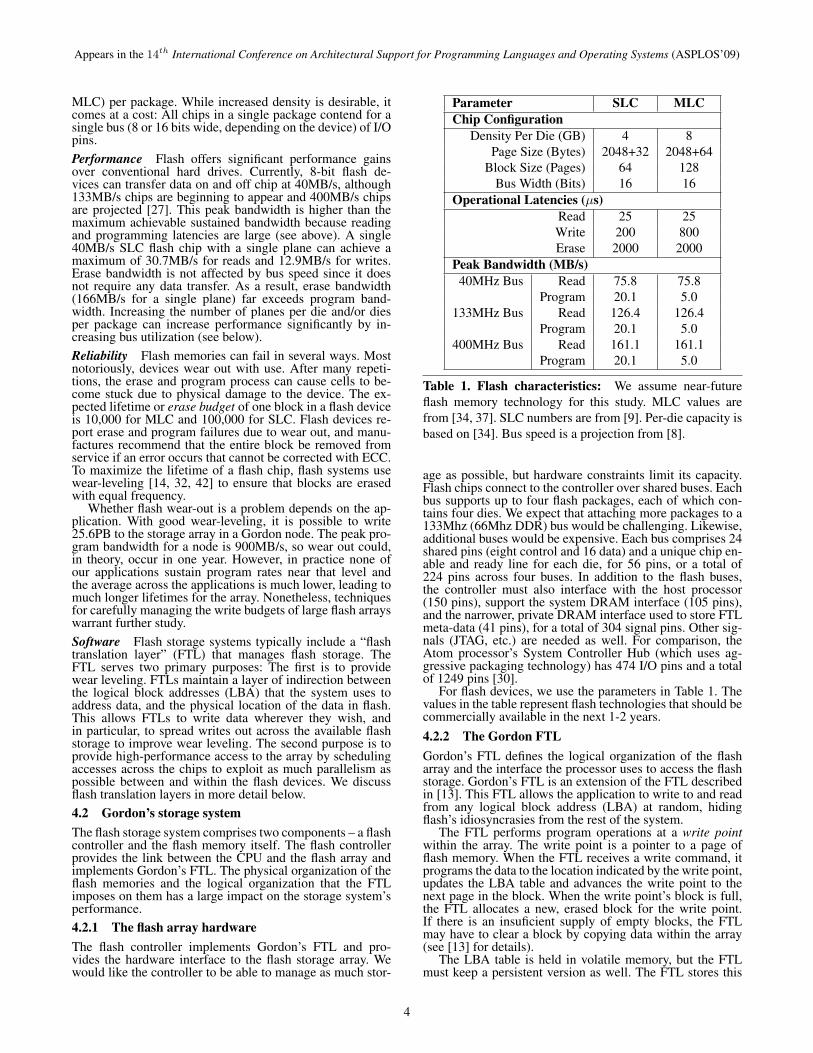
The lower-left points (circled) are the Pareto optimal nodedesigns: Shorter run times are not possible without increas-ing energy and vice versa. For all the workloads, the same de-signs are Pareto optimal. All of them are flash-based. Table 6summarizes the Pareto optimal designs and the lowest-powerdesign. The designs labeled MinT, MaxE, and MinP, are thefastest (minimum time), most efficient (performance/watt),and minimum average power configurations, respectively.
The table also summarizes the improvements in perfor-mance, efficiency, and power consumption that flash pro-vides for each configuration. For instance, MaxE is between2.2 and 2.5× more efficient than the most efficient disk con-figuration, while MinP saves over 68% in power. The gains inperformance are substantial as well: MinT is between 1.5×and 1.8× as fast as a similar disk-based system while spend-ing nearly equal energy.
8
Appears in the 14th International Conference on Architectural Support for Programming Languages and Operating Systems (ASPLOS’09)
Name CPU Average Power vs Perf/watt vs Speedup vsconfiguration Power (W) MinP Disk MaxE Disk MinT Disk
NoSync Sync NoSync Sync NoSync Sync NoSync SyncMinP 1 Atom; 0.8GHz 1.43 3.91 0.33 0.32 1.74 1.12 0.07 0.07MaxE 1 Atom; 1.9GHz 2.32 4.81 0.54 0.39 2.54 2.15 0.16 0.16
1 Core 2; 2.4GHz 9.14 19.89 2.11 1.63 2.31 1.88 0.59 0.562 Core 2; 2.4GHz 23.82 45.66 5.51 3.74 1.64 1.45 1.09 1.004 Core 2; 1.8GHz 47.56 92.74 11.00 7.59 1.11 0.92 1.48 1.29
MinT 4 Core 2; 2.4GHz 58.50 106.18 13.54 8.69 1.08 0.93 1.77 1.49
Table 6. Optimal Gordon configurations: For all three design goals (performance, performance/watt, and power consump-tion) Gordon acheives substantialy better results than disk-based designs. Results are presented for both sync and nosyncmethods. MinP is not Pareto optimal.
0
0.5
1
1.5
2
2.5
0 5 10 15 20 25 30 35
Re
lati
ve
En
erg
y
Relative Run Time
Index
0
0.5
1
1.5
2
2.5
0 5 10 15 20 25 30 35
Re
lati
ve
En
erg
y
Relative Run Time
Complex Grep Atom-Disk
Atom-Flash
Core 2-Disk
Core 2-Flash
Pareto Optimal Points
0
0.5
1
1.5
2
2.5
0 5 10 15 20 25 30 35
Re
lati
ve
En
erg
y
Relative Run Time
Ngram
0
0.5
1
1.5
2
2.5
0 5 10 15 20 25 30 35
Re
lati
ve
En
erg
y
Relative Run Time
Average
Figure 6. Parato-optimal Gordon system designs: Results of our design space survey for Index, NGram, Complex Grep,and the average across our benchmark suite. The Pareto-optimal designs are circled.
9

Appears in the 14th International Conference on Architectural Support for Programming Languages and Operating Systems (ASPLOS’09)
Figure 7 shows how the network, processor, and storagesystems contribute to execution time for MaxE and MaxE-disk, the most efficient disk-based configuration (4 Atomprocessors @ 1.9Ghz, 1 disk). The stacked bars show theportion of execution when different combinations of compo-nents are fully utilized (i.e., when those components limitperformance). The disk-based configuration spends aboutequal time disk bound (second section of the bar from thetop) as CPU bound (third from top). For the MaxE flashconfiguration, the CPU is clearly the bottleneck, but sincethe MaxE configuration is Pareto-optimal, adding additionalprocessors is not a good power/performance trade-off. TheMinT flash configuration, however, includes four processorsand its performance varies from strongly CPU bound (Com-plexGrep) to substantially disk/flash bound (Identity).5.5 Gordon power consumptionFigure 8 shows the per-component energy consumptionfor the MaxE configuration relative to MaxE-disk. Per-component energy consumption is mostly uniform across theapplications. On average, MaxE-flash consumes 40% of theenergy of the disk-based configuration, but execution timesare longer, leading to a factor of two increase in performanceper watt. The data show that the increased idle power of diskhas a twofold impact on efficiency. It causes the disk to burnexcess power, but also encourages the design to use higher-performance, less efficient processors, since these processorsreduce the amount of time the disk sits idle. Flash eliminatesthe vast majority of the storage system’s idle power, allowingthe design to take advantage of more efficient processors.
Reducing Gordon’s power consumption further is chal-lenging. DRAM and overhead power account for most of theremaining power. Reducing the amount of DRAM may bepossible, especially if the in-memory working sets of our ap-plications are small. Overhead power is a widely reportedproblem at the system level [21, 20]. Reducing this source ofwaste would benefit a wide range of systems, and make thepower savings that flash can offer even more significant.
6. DiscussionIncorporating flash memory into Gordon’s system architec-ture required us to reevaluate the trade-offs between power,performance, efficiency, and cost in the design of a Gordonnode. At a larger scale, fully exploiting the efficiency gainsthat Gordon offers requires careful considerations of larger-scale trade-offs. We explore several of the trade-offs belowand examine usage models for large Gordon systems andtheir potential roles in a large data center.6.1 Exploit disks for cheap redundancyUsing a distributed, replicated filesystem increases the costof storage for both disk and flash-based systems. We canmediate this problem for some applications by combiningGordon nodes with other servers that have conventional harddrives. Gordon’s file system can keep one replica in flashand redundant copies on disk. In the case of a failure, re-covery will be automatic. When the disk-based replicas arenot needed (the vast majority of the time) the conventionalservers can be put into deep sleep with their hard drives spundown.
This system works well for reads, since the replicas donot need to be updated. For write-intensive workloads, thereplica must be stored in flash at least temporarily, otherwisethe disk bandwidth for updating the hard drive-based replicaswould limit performance and significantly increase powerconsumption. One approach to mitigating this effect is totreat the flash storage array as a replica cache. All replicas offrequently updated data would be kept in flash, but replicasof less frequently updated data could be kept on disk. If
Capacity Cost Activepower(W)
SAS disk 300GB $340 15SATA disk 1.5TB $129 17
4GB DIMM 4GB $193 6FusionIO 160GB SLC 160GB $2000 9
2.6GHz Intel Quad core n/a $500 60Max DRAM enclosure n/a $1795 110
Max flash enclosure n/a $1025 90Max disk enclosure n/a $1600 90
Table 7. Cost and power model for commodity systems:To model the cost and power consumption of commod-ity systems, we retail pricing information for the disks andDRAM. Enclosure power data are estimates based on mea-surements of our cluster.
# of Media Non- %Non- %Non-servers cost media media media
cost cost power4GB DIMMs 10,923 $50M $41M 45% 68%
NAND 2185 $13M $3M 22% 91%SAS Disks 218 $1.2M $627K 35% 53%
SATA Disks 44 $100K $125K 54% 68%
Table 8. The fiscal and power costs of storing a petabyte:Differences in cost, performance, density, and power require-ments affect the distribution of costs across the system. Flashspends more dollars and less power on the storage media it-self, so specializing the rest of the system leads to smallerincreases in costs and greater savings in power.
writes become less frequent, the replicas could be migratedto disk. Indeed, if a piece of data has not been accessed at allin a very long time, all replicas could be moved to disk.6.2 CostCurrently, cluster-based systems rely heavily on commoditycomponents to reduce cost. For current systems that needto store very large amounts of data, this is a wise trade-off:Disks are slow and cheap, so there is little point in spendinglarge sums to provide fast processors and exotic, high-speednetworks.
Tables 7 and 8 contain a cost model and the results itgenerates to show how flash storage alters these trade-offs.The model computes the cost of storing 1PB of data inDRAM DIMMs, SLC flash-based PCIe storage cards [2],SAS disks, and commodity SATA disks. The model includesnon-storage costs, such as the enclosures needed to housethe storage media and the CPUs required to access it. Usingprices and specifications for currently-available commodityservers [41], it chooses the densest option for each storagetechnology (for DRAM, a machine with 24 DIMM slots;for disks, the machine with sixteen drive bays; for flash, amachine with four PCIe slots to accept flash storage cards).
Currently, the retail price for 160GB FusionIO devicesis $7200, but we do not believe this reflects a reasonablecost for the device they provide. In bulk, SLC flash currently
10

Appears in the 14th International Conference on Architectural Support for Programming Languages and Operating Systems (ASPLOS’09)
30%
40%
50%
60%
70%
80%
90%
100%
Exe
cu
tio
n T
ime
0%
10%
20%
30%
Ma
xE F
lash
Min
T F
lash
Ma
xE D
isk
Ma
xE F
lash
Min
T F
lash
Ma
xE D
isk
Ma
xE F
lash
Min
T F
lash
Ma
xE D
isk
Ma
xE F
lash
Min
T F
lash
Ma
xE D
isk
Ma
xE F
lash
Min
T F
lash
Ma
xE D
isk
Ma
xE F
lash
Min
T F
lash
Ma
xE D
isk
Ma
xE F
lash
Min
T F
lash
Ma
xE D
isk
index compgrep sort simplegrep identity ngram average
Exe
cu
tio
n T
ime
Parallel CPU+Flash/Disk Limited CPU Limited Flash/Disk Limited Net Limited
Figure 7. Per-component contributions to executiontime: The run-time of each benchmark broken down by theactive hardware components.
0.3
0.4
0.5
0.6
0.7
0.8
0.9
1
Re
lati
ve
En
erg
y
0
0.1
0.2
0.3
Flash Disk Flash Disk Flash Disk Flash Disk Flash Disk Flash Disk Flash Disk
index compgrep sort simpgrep identity ngram average
Re
lati
ve
En
erg
y
overhead cpu disk/flash mem
Figure 8. Relative energy consumption: Node energyconsumption for MaxE relative to the disk-based configu-ration with highest performance per watt.
costs about $5/GB ($800 for 160GB) [6], so $7200 reflectsa very large profit margin that will undoubtably diminishwith competition. We estimate the price of the 160GB PCIedevice at $2000.
The model makes it clear why commodity componentsare a good choice, especially for disk-based systems. Inthose systems between 35 and 54% of the cost is the non-storage components of the system and those components ac-count for 53-68% of power consumption. If specialized hard-ware doubled the cost of the non-disk components and re-duced their power consumption by half, the resulting ma-chine would cost 35-54% more and use 16-32% less power.Since disks are inherently slow, the gains from specializationwould likely be modest.
For NAND, specialization could cost less (22%) and leadto greater power savings (45%). Furthermore, since flashis delivers much greater raw performance than disks, theperformance gains from specialization will be greater (as ourresults for Gordon demonstrate).
We expect flash prices to continue to drop at between50 and 60% per year [40], but hard drive prices are fallingas well. However, in terms of cost per bandwidth, flash isa clear winner. Gordon’s flash array delivers over 900MB/susing ∼$1280 worth of flash at current prices. The disks fora RAID array that delivers the same bandwidth would cost$4500 and would consume 100 times more power than Gor-don’s flash storage system. As flash bus speeds increase andprices fall further, flash’s bandwidth advantage will continueto grow.
Ultimately, whether flash is an economically wise designdecision depends on the benefits it can deliver and the newapplications it can enable. Flash offers huge gains relativeto disk in terms of performance, efficiency, density and rel-ative to DRAM in terms of density and power consumption.If these gains are, for instance, sufficient to move a data-intensive application from off-line to on-line, flash could eas-ily justify its extra cost. More generally, we expect flash’s ca-pabilities to enable applications that are simply not feasiblewith conventional storage technology. This work takes thefirst step in that direction, by understanding flash’s strengthsand weakness in existing applications.
6.3 Virtualizing GordonGordon’s strength is providing high-bandwidth, highly-parallel access to large volumes of data, not in storing that
data. For storage, disks are more cost effective. This meansthat a Gordon system is being effectively utilized if the data itstores are being accessed frequently. Consequently, it makessense to manage Gordon systems to maximize bandwidthutilization.
For some latency-critical workloads and workloads thatneed to process all the data stored by a group or organization,it will make sense to store data in a Gordon system andprocess it in place. In other scenarios, we imagine that thetotal data stored will be much larger than Gordon’s capacity.In these cases, we will virtualize the Gordon system so itsdata-processing abilities can be brought to bear on muchlarger data sets than it can store.
This usage model treats all or part of a Gordon systemas a specialized co-processor for performing computationson a small part of a much larger quantity of data stored in adisk-based “data warehouse.” Before a job runs, Gordon willload the necessary data into flash storage, and once the jobcompletes, data for another job will take its place.
For instance, a 1024-node system could be partitionedinto 16, 64-node slices, each with NVM storage for 16TBof data. Each slice provides a total of 112GB/s of I/O band-width. Assuming dual 1Gb network connections between theGordon slice and the data warehouse, loading 10TB of data(leaving room for scratch data in the flash storage array)would take about 11 hours. Gordon would perform the com-putations on the data, transfer the results to the warehouseand load the data for the next job. Network limitations meanthat transfering data between the Gordon array and the ware-house utilizes only 0.4% of Gordon’s bandwidth resources.We can improve the situation by overlapping data transferwith execution and reducing the storage space allocated toeach job by 50% (to accomodate storing both data sets si-multaneously). The impact on execution time would be min-imal, and if jobs spent at least 4 seconds processing each GBof data, the time cost of loading the next job would be fullyhidden by useful processing.
7. ConclusionThis paper has presented Gordon, a flash memory-basedcluster architecture for large-scale data-intensive applica-tions. We describe a flash-based system that is carefullytuned for data-intensive applications. Gordon systems com-bine this storage array with a conventional low-power pro-cessor and programming abstractions for large-scale dis-
11

Appears in the 14th International Conference on Architectural Support for Programming Languages and Operating Systems (ASPLOS’09)
tributed programming. The result is a highly-efficient, high-performance, highly-parallel computing system that is easyto use.
Compared to disk-based systems, Gordon systems are1.5× faster and deliver 2.5× more performance per watt. Asflash performance improves, these performance gains willonly increase. Gordon demonstrates that flash affords theopportunity to re-engineer many aspects of system design,and, therefore, enables a new class of computing systems.
AcknowledgementsThe authors would like to thank the ASPLOS program com-mittee reviewers as well Nathan Goulding and Joel Coburnfor their helpful comments. This work is supported in part byNSF awards NSF0811794 and NSF0643880.References
[1] http://hadoop.apache.org/core/.[2] http://www.fusionio.com/.[3] http://xtreview.com/addcomment-id-4801-view-Intel-atom-
1.6-Ghz-benchmark.html.[4] http://laptoping.com/intel-atom-benchmark.html.[5] http://www.vmware.com/.[6] DRAMeXchange. http://www.dramexchange.com/.[7] Open nand flash interface specification 1.0.
http://www.onfi.org/documentation.html.[8] Open nand flash interface specification 2.0.
http://www.onfi.org/documentation.html.[9] Samsung k9f8g08uxm flash memory datasheet.
[10] Samsung debuts 64gbit mlc nand flashmemory. EE Times Asia, October 2007.http://www.eetasia.com/ART 8800485916 499486 NP -11c4687c.HTM.
[11] New intel centrino atom processor technology ushers in ’bestinternet experience in your pocket’, 2008. Intel Press release.
[12] N. Agrawal, V. Prabhakaran, T. Wobber, J. D. Davis, M. Man-asse, and R. Panigrahy. Design tradeoffs for ssd performance.June 2008.
[13] A. Birrell, M. Isard, C. Thacker, and T. Wobber. A designfor high-performance flash disks. Technical Report MSR-TR-2005-176, Microsoft Research, December 2005.
[14] L.-P. Chang. On efficient wear leveling for large-scale flash-memory storage systems. In SAC ’07: Proceedings of the2007 ACM symposium on Applied computing, pages 1126–1130, New York, NY, USA, 2007. ACM.
[15] H. chih Yang, A. Dasdan, R.-L. Hsiao, and D. S. Parker. Map-reduce-merge: simplified relational data processing on largeclusters. In SIGMOD ’07: Proceedings of the 2007 ACMSIGMOD international conference on Management of data,pages 1029–1040, New York, NY, USA, 2007. ACM.
[16] C. T. Chu, S. K. Kim, Y. A. Lin, Y. Yu, G. R. Bradski, A. Y.Ng, and K. Olukotun. Map-reduce for machine learning onmulticore. In B. Scholkopf, J. C. Platt, and T. Hoffman,editors, NIPS, pages 281–288. MIT Press, 2006.
[17] J. Dean and S. Ghemawat. Mapreduce: simplified dataprocessing on large clusters. In OSDI’04: Proceedings of the6th conference on Symposium on Opearting Systems Design& Implementation, pages 10–10, Berkeley, CA, USA, 2004.USENIX Association.
[18] D. DeWitt and J. Gray. Parallel database systems: the futureof high performance database systems. Commun. ACM,35(6):85–98, 1992.
[19] D. J. Dewitt, S. Ghandeharizadeh, D. A. Schneider, A. Bricker,H. I. Hsiao, and R. Rasmussen. The gamma database machineproject. IEEE Trans. on Knowl. and Data Eng., 2(1):44–62,1990.
[20] D. Economou, S. Rivoire, C. Kozyrakis, and P. Ranganathan.Full-system power analysis and modeling for server environ-ments. June 2006.
[21] X. Fan, W.-D. Weber, and L. A. Barroso. Power provisioningfor a warehouse-sized computer. In ISCA, pages 13–23, NewYork, NY, USA, 2007. ACM.
[22] Y. Fukuzumi, Y. Matsuoka, M. Kito, M. Kido, M. Sato,H. Tanaka, Y. Nagata, Y. Iwata, H. Aochi, and A. Nitayama.Optimal integration and characteristics of vertical array de-vices for ultra-high density, bit-cost scalable flash memory.
Electron Devices Meeting, 2007. IEDM 2007. IEEE Interna-tional, pages 449–452, 10-12 Dec. 2007.
[23] G. Ganger, B. Worthington, and Y. Patt. Disksim.http://www.pdl.cmu.edu/DiskSim/.
[24] S. Ghemawat, H. Gobioff, and S.-T. Leung. The google filesystem. SIGOPS Oper. Syst. Rev., 37(5):29–43, 2003.
[25] G. Graefe. Encapsulation of parallelism in the volcano queryprocessing system. SIGMOD Rec., 19(2):102–111, 1990.
[26] T. R. Halfhill. Intel’s tiny atom. Microprocssor Report, April2008.
[27] A. Huffman. Onfi: Leading the way to higher performance.http://www.onfi.org/docs/ComputexDRAMeXchange.pdf.
[28] Intel. Increasing data center density while driving down powerand cooling costs, June 2006. White paper.
[29] Intel. Quad-core intel xeon processor 3200 series datasheet,2007.
[30] Intel. Intel system controller hub datasheet, 2008.http://download.intel.com/design/chipsets/embedded-/datashts/319537.pdf.
[31] M. Isard, M. Budiu, Y. Yu, A. Birrell, and D. Fetterly. Dryad:distributed data-parallel programs from sequential buildingblocks. SIGOPS Oper. Syst. Rev., 41(3):59–72, 2007.
[32] D. Jung, Y.-H. Chae, H. Jo, J.-S. Kim, and J. Lee. Agroup-based wear-leveling algorithm for large-capacity flashmemory storage systems. In CASES, pages 160–164, NewYork, NY, USA, 2007. ACM.
[33] S.-M. Jung, J. Jang, W. Cho, H. Cho, J. Jeong, Y. Chang,J. Kim, Y. Rah, Y. Son, J. Park, M.-S. Song, K.-H. Kim, J.-S.Lim, and K. Kim. Three dimensionally stacked nand flashmemory technology using stacking single crystal si layerson ild and tanos structure for beyond 30nm node. ElectronDevices Meeting, 2006. IEDM ’06. International, pages 1–4,11-13 Dec. 2006.
[34] D. Kwak, J. Park, K. Kim, Y. Yim, S. Ahn, Y. Park, J. Kim,W. Jeong, J. Kim, M. Park, B. Yoo, S. Song, H. Kim, J. Sim,S. Kwon, B. Hwang, H. kyu Park, S. Kim, Y. Lee, H. Shin,N. Yim, K. Lee, M. Kim, Y. Lee, J. Park, S. Park, J. Jung,and K. Kim. Integration technology of 30nm generationmulti-level nand flash for 64gb nand flash memory. VLSITechnology, 2007 IEEE Symposium on, pages 12–13, 12-14June 2007.
[35] A. W. McNabb, C. K. Monson, and K. D. Seppi. Mrpso:Mapreduce particle swarm optimization. In GECCO ’07:Proceedings of the 9th annual conference on Genetic andevolutionary computation, pages 177–177, New York, NY,USA, 2007. ACM.
[36] Micron. Micron ddr3 sdrammt41j256m8 datasheet rev d, 2008.http://download.micron.com/pdf/datasheets/dram/ddr3/2GbDDR3 SDRAM.pdf.
[37] Y. Park, J. Choi, C. Kang, C. Lee, Y. Shin, B. Choi, J. Kim,S. Jeon, J. Sel, J. Park, K. Choi, T. Yoo, J. Sim, and K. Kim.Highly manufacturable 32gb multi-level nand flash memorywith 0.0098 µm2 cell size using tanos(si - oxide - al2o3 - tan)cell technology. Electron Devices Meeting, 2006. IEDM ’06.International, pages 1–4, 11-13 Dec. 2006.
[38] C. Ranger, R. Raghuraman, A. Penmetsa, G. Bradski, andC. Kozyrakis. Evaluating mapreduce for multi-core and mul-tiprocessor systems. In HPCA ’07: Proceedings of the 2007IEEE 13th International Symposium on High PerformanceComputer Architecture, pages 13–24, Washington, DC, USA,2007. IEEE Computer Society.
[39] R. Schuetz, H. Oh, J.-K. Kim, H.-B. Pyeon, S. Przybylski,and P. Gillingham. Hyperlink nand flash architecture for massstorage applications. Non-Volatile Semiconductor MemoryWorkshop, 2007 22nd IEEE, pages 3–4, 26-30 Aug. 2007.
[40] A. Shah. PC World, February 2008.http://www.pcworld.com/article/id,142684-page,1/article.html.
[41] http://www.supermicro.com/products/system/.[42] D. Woodhouse. Jffs2: The journalling flash file system,
version 2. http://sources.redhat.com/jffs2/.
12