Embed Size (px)
Citation preview
HAL Id: tel-00280968https://tel.archives-ouvertes.fr/tel-00280968
Submitted on 20 May 2008
HAL is a multi-disciplinary open accessarchive for the deposit and dissemination of sci-entific research documents, whether they are pub-lished or not. The documents may come fromteaching and research institutions in France orabroad, or from public or private research centers.
L’archive ouverte pluridisciplinaire HAL, estdestinée au dépôt et à la diffusion de documentsscientifiques de niveau recherche, publiés ou non,émanant des établissements d’enseignement et derecherche français ou étrangers, des laboratoirespublics ou privés.
Génération numérique de signaux RF pour les terminauxde communication mobile par modulation delta-sigma
Antoine Frappé
To cite this version:Antoine Frappé. Génération numérique de signaux RF pour les terminaux de communication mobilepar modulation delta-sigma. Micro and nanotechnologies/Microelectronics. Université des Scienceset Technologie de Lille - Lille I, 2007. English. tel-00280968

UNIVERSITE DES SCIENCES ET
TECHNOLOGIES DE LILLE
Ecole Doctorale Sciences Pour l’Ingénieur
THESE En vue de l’obtention du grade de
DOCTEUR DE L’UNIVERSITE DE LILLE
Discipline : Electronique
Présentée et soutenue publiquement le 7 décembre 2007 par
Antoine FRAPPÉ
ALL-DIGITAL RF SIGNAL GENERATION USING
∆Σ MODULATION FOR MOBILE
COMMUNICATION TERMINALS
GENERATION NUMERIQUE DE SIGNAUX RF
POUR LES TERMINAUX DE COMMUNICATION
MOBILE PAR MODULATION ∆Σ
Jury : M. Paul-Alain ROLLAND Président M Michiel STEYAERT Rapporteur M. Patrick LOUMEAU Rapporteur M. Andreas KAISER Directeur de thèse
Mme Andreia CATHELIN Examinateur M. Bruno STEFANELLI Examinateur

i
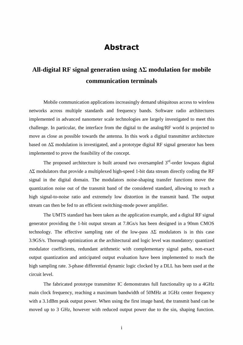
Abstract
All-digital RF signal generation using ∆Σ modulation for mobile
communication terminals
Mobile communication applications increasingly demand ubiquitous access to wireless
networks across multiple standards and frequency bands. Software radio architectures
implemented in advanced nanometer scale technologies are largely investigated to meet this
challenge. In particular, the interface from the digital to the analog/RF world is projected to
move as close as possible towards the antenna. In this work a digital transmitter architecture
based on ∆Σ modulation is investigated, and a prototype digital RF signal generator has been
implemented to prove the feasibility of the concept.
The proposed architecture is built around two oversampled 3rd-order lowpass digital
∆Σ modulators that provide a multiplexed high-speed 1-bit data stream directly coding the RF
signal in the digital domain. The modulators noise-shaping transfer functions move the
quantization noise out of the transmit band of the considered standard, allowing to reach a
high signal-to-noise ratio and extremely low distortion in the transmit band. The output
stream can then be fed to an efficient switching-mode power amplifier.
The UMTS standard has been taken as the application example, and a digital RF signal
generator providing the 1-bit output stream at 7.8Gs/s has been designed in a 90nm CMOS
technology. The effective sampling rate of the low-pass ∆Σ modulators is in this case
3.9GS/s. Thorough optimization at the architectural and logic level was mandatory: quantized
modulator coefficients, redundant arithmetic with complementary signal paths, non-exact
output quantization and anticipated output evaluation have been implemented to reach the
high sampling rate. 3-phase differential dynamic logic clocked by a DLL has been used at the
circuit level.
The fabricated prototype transmitter IC demonstrates full functionality up to a 4GHz
main clock frequency, reaching a maximum bandwidth of 50MHz at 1GHz center frequency
with a 3.1dBm peak output power. When using the first image band, the transmit band can be
moved up to 3 GHz, however with reduced output power due to the sinc shaping function.

ii
With a 2.6GHz main clock frequency and 5MHz WCDMA modulated channel at a carrier
frequency of 650MHz, a channel output power of -3.9dBm and 53.6dB of ACPR are
obtained. With the same settings, a channel output power of -15.8dBm and an ACPR of
44.3dB is reached in the 1.95GHz image band, which fulfills minimum UMTS requirements.
The chip size is 4×0.8mm² and it has an active area of 0.15mm². Its power consumption is
69mW for a 2.6GHz operating clock frequency.
Keywords: delta-sigma modulation, digital transmitter, redundant arithmetic, software
radio, RF, UMTS, switching-mode power amplifier, 90nm CMOS.
This thesis work has been performed in the Integrated Circuits Design Group /
Microélectronique Silicium of the ISEN department of the Institut d’Electronique, de
Microélectronique et de Nanotechnologies (IEMN), 41, bd Vauban, 59000 Lille, France.

iii
Résumé
Génération numérique de signaux RF pour les terminaux de
communication mobile par modulation delta-sigma
Les appareils de communications mobiles demandent de plus en plus un accès
omniprésent aux réseaux sans fils à travers différents standards et bandes de fréquences. Les
architectures radio-logicielles, conçues dans des technologies nanométriques avancées, sont
très largement étudiées pour atteindre cet objectif. En particulier, l’interface entre les mondes
numériques et analogiques/RF semble se déplacer au plus proche de l’antenne. Dans ce
travail, une architecture de transmetteur numérique, basée sur la modulation ∆Σ, est étudiée et
un prototype de générateur de signaux RF numériques a été fabriqué pour prouver ce concept.
L’architecture proposée est construite autour de deux modulateurs ∆Σ passe-bas
suréchantillonnés du 3ème ordre qui fournissent un signal multiplexé sur 1 bit à haute cadence,
qui code directement le signal RF dans le domaine numérique. Les fonctions de transfert des
modulateurs comportent une mise en forme du bruit de quantification pour le déplacer en
dehors de la bande d’émission du standard considéré, permettant ainsi d’atteindre un rapport
signal-à-bruit élevé et peu de distorsion dans la bande d’émission. La séquence de sortie peut
ensuite être appliquée à l’entrée d’un amplificateur de puissance commuté ayant une bonne
efficacité.
Le standard UMTS a été choisi comme exemple d’application et un générateur de
signaux RF numérique, fournissant un signal de sortie sur 1 bit à 7.8Géch/s a été réalisé dans
une technologie 90nm CMOS. La cadence d’échantillonnage effective des modulateurs ∆Σ
passe-bas est dans ce cas de 3.9Géch/s. Une optimisation approfondie au niveau architectural
et au niveau logique a été obligatoire : une quantification des coefficients des modulateurs,
une arithmétique redondante comprenant des signaux complémentaires, une quantification de
sortie non exacte et une évaluation anticipée de la sortie ont été implémentés pour parvenir à
la cadence désirée. Une logique dynamique différentielle sur 3 phases d’horloge, générées par
une DLL, a été utilisée au niveau circuit.
iv
Le circuit intégré du transmetteur prototype démontre une fonctionnalité complète
jusqu’à une fréquence d’horloge de 4GHz, permettant ainsi d’atteindre une bande passante
maximum de 50MHz autour d’une fréquence porteuse de 1GHz avec une puissance de sortie
en pic de 3.1dBm. Si la première bande image est utilisée, la bande d’émission peut être
déplacée jusqu’à 3GHz, avec cependant une puissance de sortie réduite à cause de la fonction
de mise en forme du sinus cardinal. Avec une fréquence d’horloge de 2.6GHz et un canal
WCDMA de 5MHz modulé autour d’une fréquence porteuse de 650MHz, la puissance de
canal en sortie est de -3.9dBm et 53.6dB d’ACLR sont obtenus. Avec les mêmes paramètres,
la puissance du canal en sortie est de -15.8dBm et un ACPR de 44.3dB est atteint pour la
bande image à 1.95GHz, ce qui rentre dans les spécifications UMTS. Les dimensions du
circuit sont 4×0.8mm², tandis que l’aire active est de 0.15mm². La consommation du circuit
est de 69mW sous 1V pour une fréquence d’horloge de 2.6GHz.
Mots-clés : modulation delta-sigma, transmetteur numérique, arithmétique
redondante, radio logicielle, RF, UMTS, amplificateur de puissance commuté, CMOS 90nm.
Thèse preparée dans l’equipe Conception de Circuits Intégrés / Microélectornique
Silicium du Département ISEN de l’Institut d’Electronique, de Microélectronique et de
Nanotechnologies (IEMN), 41, bd Vauban, 59000 Lille.

v
Acknowledgments
“With a little help from my friends” (John Lennon and Paul McCartney)
I wish to thank people from the electronic team:
Andreas Kaiser, my thesis director, for his guidance, support and his constant
motivation to probe further;
Bruno Stefanelli, for his collaborative efforts on chip design and layout;
Valérie Vandenhende, for her administrative support;
Jean-Marc Capron, for interesting discussions;
Axel Flament, for the fun he brings and the friendly work we have made;
And Manu, Droudrou, Sophie, Jean, Crépin, Christophe, Fanou, Sophie, Ben, Dimitri,
Patrick …
I will miss you when I will leave.
A great acknowledgement to Raphael Daouphars, who sets me on the way to many
improvements in my work;
I also thank the faculty of ISEN and IEMN, for its hearty welcome;
Thanks to Andreia Cathelin and her team at STMicroelectronics for interesting
meetings and for the access to state-of-the-art technology processes;
Thanks to subcontractors, especially CIBEL firm and Mr Gamberini, for their
successful attempts on restrictive assemblies;
Many thanks to Rédha Kassi and Christophe Loyez, from IRCICA, for test facilities;
Thanks to my friends and my family for everyday support;
Thanks to every person who followed this work, closely or by far.


vii
Contents
Abstract ....................................................................................................... i
Résumé .....................................................................................................iii
Acknowledgments............................................................................................... v
Contents ....................................................................................................vii
Glossary of acronyms........................................................................................ xi
List of figures ..................................................................................................xvii
List of tables ................................................................................................... xxi
Introduction ...................................................................................................... 1
Chapter 1 Background................................................................................. 5
1.1 Software defined radio .............................................................................................. 5 1.1.1 Universality of RF transmitters ......................................................................... 5 1.1.2 Ideal software radio........................................................................................... 6
1.2 State-of-the-art in transmitter architectures............................................................... 7 1.2.1 Analog front-end architectures.......................................................................... 7 1.2.2 Digital IF architectures...................................................................................... 9 1.2.3 Digital RF architectures .................................................................................. 10
1.3 UMTS standard specifications ................................................................................ 11 1.3.1 Introduction to UMTS..................................................................................... 12
1.3.1.1 Protocol layers............................................................................................. 12 1.3.1.2 Access mode and frequency allocation ....................................................... 13
1.3.2 UMTS specifications for transmitters ............................................................. 15 1.3.2.1 Spectrum emission mask............................................................................. 15 1.3.2.2 Adjacent Channel Leakage Power Ratio..................................................... 16 1.3.2.3 Spurious emissions...................................................................................... 17 1.3.2.4 Error Vector Magnitude .............................................................................. 18
1.4 Conclusion............................................................................................................... 19
Chapter 2 Digital transmitter architecture.............................................. 21
2.1 Global transmitter architecture................................................................................ 21
viii
2.1.1 Transmitter architecture and frequency planning............................................ 21 2.1.2 Digital upconversion and noise-shaping architecture ..................................... 26 2.1.3 Power amplifier and antenna filters ................................................................ 30
2.1.3.1 Switching-mode power amplifier topology................................................. 30 2.1.3.2 Power DAC non-idealities .......................................................................... 32 2.1.3.3 Antenna filters ............................................................................................. 34
2.2 UMTS implementation case of the digital transmitter ............................................ 36 2.2.1 Proposed digital transmission chain................................................................ 36 2.2.2 Baseband processing ....................................................................................... 36 2.2.3 Sample rate conversion ................................................................................... 39 2.2.4 Digital ∆Σ modulators..................................................................................... 41
2.2.4.1 Lowpass ∆Σ modulator architecture ........................................................... 41 2.2.4.2 Simulated performances.............................................................................. 43
2.3 Conclusion............................................................................................................... 44
Chapter 3 Delta-Sigma modulator system design ................................... 47
3.1 ∆Σ architecture optimization................................................................................... 48 3.2 Logic design issues.................................................................................................. 50
3.2.1 Critical path and digital implementation issues .............................................. 50 3.2.2 Adder architectures analysis............................................................................ 52 3.2.3 Circuit level adders design considerations ......................................................54
3.3 ∆Σ architecture with redundant arithmetic.............................................................. 56 3.3.1 Redundant number representation................................................................... 56 3.3.2 Structures for redundant addition.................................................................... 57 3.3.3 ∆Σ modulator architecture in BS representation ............................................. 61 3.3.4 Simulation results............................................................................................ 64
3.4 Output quantizer in Borrow-Save arithmetic .......................................................... 65 3.4.1 Non-exact quantization ................................................................................... 65 3.4.2 Output signal precomputation ......................................................................... 69
3.5 Conclusion............................................................................................................... 70
Chapter 4 Digital transmitter circuit design............................................ 73
4.1 Transmitter IC description ...................................................................................... 73 4.1.1 IC structure...................................................................................................... 73 4.1.2 IC configuration and layout............................................................................. 74
4.2 Sample rate conversion block design ...................................................................... 75 4.2.1 Block structure ................................................................................................ 75 4.2.2 TSPCFF registers ............................................................................................ 78
4.3 Digital delta-sigma modulator circuit design .......................................................... 81 4.3.1 Global structure ............................................................................................... 81 4.3.2 Dynamic FA circuit description ...................................................................... 82 4.3.3 Initialization circuitry...................................................................................... 84 4.3.4 ∆Σ modulator layout view............................................................................... 86
4.4 Clock generation and distribution ........................................................................... 88 4.4.1 Controlled delay line description .................................................................... 89 4.4.2 Phase comparator and charge pump................................................................90 4.4.3 DLL mechanism and clock signals characteristics ......................................... 91
4.5 Digital mixer and output stages design ................................................................... 93 4.5.1 Digital mixer structure .................................................................................... 94

ix
4.5.2 Output stages ................................................................................................... 95 4.6 Conclusion............................................................................................................... 96
Chapter 5 Experimental results ................................................................ 97
5.1 First prototype IC (FULBERT I) ............................................................................ 97 5.1.1 Test hardware description ............................................................................... 97
5.1.1.1 Measurement tools ...................................................................................... 97 5.1.1.2 Test boards and assembly............................................................................ 98
5.1.2 Measurement results...................................................................................... 100 5.1.2.1 Issues ......................................................................................................... 100 5.1.2.2 Output stages measurements ..................................................................... 102
5.2 Second prototype IC (FULBERT II)..................................................................... 103 5.2.1 Changes and enhancements........................................................................... 103 5.2.2 Test hardware description ............................................................................. 105 5.2.3 Measurement results...................................................................................... 106
5.2.3.1 Core functionality...................................................................................... 107 5.2.3.2 Measurement results at a 2.6GHz main clock frequency.......................... 108
Frequency Spectra ................................................................................................. 108 ACPR vs Channel Power ...................................................................................... 111 SNDR vs Channel Power ...................................................................................... 113 EVM measurements .............................................................................................. 114 Output Jitter........................................................................................................... 115 Summary of measurements with a 2.6GHz main clock ........................................ 116
5.2.3.3 Measurements at other frequencies ........................................................... 117 Power consumption ............................................................................................... 117 Evolution of ACPR ............................................................................................... 118 Evolution of SNDR ............................................................................................... 120 Evolution of EVM................................................................................................. 121 Evolution of the channel power ............................................................................ 122 Evolution of the jitter ............................................................................................ 123 Summary of measurements ................................................................................... 123
5.2.4 Comparison with similar works .................................................................... 124 5.3 Conclusion............................................................................................................. 125
Conclusion .................................................................................................. 127
Parallel works........................................................................................................ 127 Reconfigurability................................................................................................... 128 Future directions.................................................................................................... 129
Bibliography .................................................................................................. 131
Résumé en français..............................................................................................I
Contexte ..................................................................................................................... I Architecture du transmetteur numérique................................................................. III Conception système du modulateur ∆Σ ..................................................................VI Conception circuit du transmetteur numérique .................................................... VIII Résultats expérimentaux .......................................................................................... X Conclusion..............................................................................................................XII

x

xi
Glossary of acronyms
∆Σ Delta-Sigma
3G Third Generation of mobile phone wireless systems
4G Fourth Generation of mobile phone wireless systems
ACLR Adjacent Channel Leakage Ratio
ACPR Adjacent Channel Power Ratio
ADC Analog-to-Digital Conversion/Converter
AWG Arbitrary Waveform Generator
BAW Bulk Acoustic Wave
BP BandPass
BPF BandPass Filter
BS Borrow-Save
BSD Binary Signed-Digit
C2 Two’s complement
CDMA Code Division Multiple Access
CDMA2000 Code Division Multiple Access 3G US standard
CIC Cascade Integrator Comb
CIFB Cascade of Integrators with FeedBacks
CIFF Cascade of Integrators with FeedForwards
CLA Carry-LookAhead adder
CLK Clock
CMOS Complementary Metal Oxide Semiconductor
CORDIC Coordinate Rotation Digital Computing
CPL Complementary Pass-transistor Logic
CSA Carry-Save adder
CSK Carry-Skip adder
CSL Carry-SeLect adder

xii
DAC Digital-to-Analog Conversion/Converter
dBc Power referenced to a carrier power, expressed in decibels
dBFS Power referenced to a full-scale sine wave, expressed in decibels
dBm Power referenced to 1 milliWatt, expressed in decibels
DC Direct Current
DCO Digitally Controlled Oscillator
DCS Digital Cellular System
DDR Double Data Rate
DECT Digital Enhanced Cordless Telecommunications
DLL Delay Locked Loop
DPCCH Dedicated Physical Control CHannel
DPDCH Dedicated Physical Data CHannel
DPL Double Pass-transistor Logic
DRFC Digital-to-RF Converter/Conversion
DS-CDMA Direct-Sequence Code Division Multiple Access
DS-SS Direct-Sequence Spread Spectrum
DSP Digital Signal Processing/Processor
DUT Device Under Test
ENOB Effective Number Of Bits
ETSI European Telecommunications Standards Institute
EVM Error Vector Magnitude
FA Full-Adder
FAMMP Minus-Minus-Plus Full-Adder
FAPPM Plus-Plus-Minus Full-Adder
FDD Frequency Division Duplex
FFT fast Fourier Transform
FIR Finite Impluse Response
FH-SS Frequency Hopping Spread Sprectrum
FPGA Field Programmable Gate Array

xiii
FS Full-Scale
GSM Global System for Mobile communications
GS/s Giga Samples per second
HA Half-Adder
HiperLAN2 High Performance Radio Local Area Network type 2
HPSK Hybrid Phase Shift Keying
IEEE Institute of Electrical and Electronics Engineers
IEEE802.11 Technology associated with WLAN defined by IEEE
IEEE802.20 Technology associated with MBWA defined by IEEE
IC Integrated Circuit
IF Intermediate Frequency
INS Integral Noise Shaping
IS-95 Interim Standard 95 (known as cdmaOne)
ISI Inter-Symbol Interference
I/O Input/Output
LO Local Oscillator
LP LowPass
LPDSM Low-Pass Delta-Sigma Modulator
LPF LowPass Filter
LSB Least Significant Bit
MAC Medium Access Control
MBWA Mobile Broadband Wireless Access
Mc/s Mega chips per second
MCC Manchester Carry Chain
MS/s Mega Samples per second
MSB Most Significant Bit
MUX Multiplexer
NMOS N-type Metal Oxide Semiconductor
NTF Noise Transfer Function

xiv
PA Power Amplifier
PAPR Peak-to-Average Power Ratio
PCB Printed Circuit Board
PHS Personal Handy-phone System
PHY PHYsical layer
PMOS P-type Metal Oxide Semiconductor
PN Pseudo-Noise
PWM Pulse Width Modulation
QPSK Quaternary Phase Shift Keying
RCA Ripple Carry Adder
RF Radio Frequency
RLC Radio Link Control
RRC Radio Ressource Control
RRC Root-Raised Cosine
RS Reset-Set
RX Reception
S/P Serial-to-Parallel
SD-r Signed-Digit adder in base r
SDR Software Defined Radio
SFDR Spurious Free Dynamic Range
SiP System in Package
SNDR Signal-to-Noise and Distortion Ratio
SNR Signal-to-Noise Ratio
SRC Sample Rate Conversion/Converter
STF Signal Tranfer Function
SoC System on Chip
TDCDMA Time Division Code Division Multiple Access
TDD Time Division Duplex
TSPCFF True Single-Phase Clock Flip-Flop

xv
TX Transmission
UE User Equipment
UMTS Universal Mobile Telecommunications System
VHDL Very high speed IC Hardware Description Language
WCDMA Wideband Code Division Multiple Access
Wi-Fi Wireless Fidelity
Wimax Worldwide Interoperability for Microwave Access
WLAN Wireless Local Area Network


xvii
List of figures
Figure 1-1 Ideal software-defined radio transmitter.................................................................. 6 Figure 1-2 Toward RF digital processing and software radio.................................................... 7 Figure 1-3 Heterodyne transmitter architecture ......................................................................... 8 Figure 1-4 Homodyne transmitter architecture .......................................................................... 8 Figure 1-5 Digital-IF transmitter architecture............................................................................ 9 Figure 1-6 Digital quadrature modulator from [10] ................................................................... 9 Figure 1-7 Conceptual block diagram of the digital-IF heterodyne transmitter from [12] ...... 10 Figure 1-8 Digital RF transmitter chain ................................................................................... 10 Figure 1-9 DSP-based wireless transmitter architecture from [5]............................................ 11 Figure 1-10 Radio interface protocol structure [22]................................................................. 12 Figure 1-11 Examples of access modes for GSM, UMTS TDD and FDD.............................. 14 Figure 1-12 Example of a RRC-shaped UMTS channel.......................................................... 15 Figure 1-13 UMTS spectrum emission mask (related to a 1MHz measurement bandwidth).. 16 Figure 1-14 UMTS spurious requirements............................................................................... 18 Figure 1-15 Amplitude and phase errors defining EVM.......................................................... 19 Figure 2-1 Digital transmitter architecture. chipf is the chip rate, cf the carrier frequency and
sf the sampling frequency............................................................................................... 21
Figure 2-2 Modulator output spectrum for channels at the lowest band edge for (a) direct conversion and (b) two-step conversion........................................................................... 22
Figure 2-3 Two-step upconversion transmitter architecture. L is a factor dependent over the chosen standard. ............................................................................................................... 23
Figure 2-4 Digital mixer operation. The sample rate is cf×4 and ,...12,8,4,0=n ................. 24
Figure 2-5 Possible architectures for noise shaper and upconverter: a) Bandpass ∆Σ modulator; b) Lowpass ∆Σ modulators............................................................................ 26
Figure 2-6 Simplified architecture if only one sample on two is computed inside the ∆Σ modulators. The ∆T delay is equal to cf41 .................................................................... 27
Figure 2-7 Frequency spectrum of the output of the digital upconverter when no interpolation is done on Q channel, showing the image that appears.................................................... 28
Figure 2-8 Architecture if the ∆Σ modulators sampling clocks are synchronous.................... 28 Figure 2-9 Chosen architecture using a linear interpolation on Q channel. ∆T’ delay is equal
to cf21 ............................................................................................................................ 29
Figure 2-10 Digital upconverter output spectrum. 8th channel is chosen. 0dBFS refers to a full-scale sine wave. ................................................................................................................ 30
Figure 2-11 On the left, schematic of the output inverter; on the right, a diagram showing the repartition of the power supply ........................................................................................ 31
Figure 2-12 Inter-symbol interference: a) with symmetric fronts; b) with asymmetric fronts 32 Figure 2-13 Output spectra for ideal, single-ended and differential outputs ...........................33 Figure 2-14 Example of ACLR variations, for 5 and 10 MHz offset channels, related to
random jitter variance....................................................................................................... 34 Figure 2-15 Digital RF output reported to the antenna (the standard measurement bandwidth
has been respected (Table 1-3)) and UMTS spectrum requirements. .............................. 35 Figure 2-16 Proposed transmitter chain ................................................................................... 36
xviii
Figure 2-17 Baseband processing blocks ................................................................................. 37 Figure 2-18 Baseband signals at each step of the baseband processing................................... 38 Figure 2-19 Spectrum of the IQ baseband output signal (9th channel is chosen arbitrarily).
Amplitude is referred to 0dBFS (full-scale sine wave). .................................................... 39 Figure 2-20 Sample rate conversion blocks ............................................................................. 40 Figure 2-21 Spectrums of the 3.9GS/s SRC output signals for the two configurations
previously cited. In red, the estimated shaped quantization noise brought by the ∆Σ modulator. ........................................................................................................................ 40
Figure 2-22 (a) Pole-zero diagram (pole: x; zero: o); (b) NTF (red) and STF (green) of the generated ∆Σ modulator (frequency is normalized to fs=3.9GHz); (c) zoom on the bandwidth (fb=30MHz) .................................................................................................... 41
Figure 2-23 Third-order ∆Σ modulator architecture ................................................................ 42 Figure 2-24 ∆Σ modulator output spectrum............................................................................. 43 Figure 2-25 Simulated SNDR for the ideal configuration ....................................................... 44 Figure 3-1 Third-order ∆Σ modulator architecture .................................................................. 48 Figure 3-2 Optimized ∆Σ architecture. The accumulator has been replaced by an integrator. 49 Figure 3-3 SNDR comparison for ideal and simplified architecture ....................................... 49 Figure 3-4 ∆Σ modulator architecture showing data registers ................................................. 50 Figure 3-5 Critical path ............................................................................................................ 51 Figure 3-6 Architecures for 4-inputs additions ........................................................................ 51 Figure 3-7 4-bit Ripple Carry Adder architecture.................................................................... 52 Figure 3-8 Carry combinational logic and STMicroelectronics 90nm design kit static logic
implementation................................................................................................................. 54 Figure 3-9 DPL gates and full-adder implementation [48] ...................................................... 55 Figure 3-10 Dot notation of two’s complement, Carry-Save and Borrow-Save representation
.......................................................................................................................................... 57 Figure 3-11 Addition in two’s complement ............................................................................. 58 Figure 3-12 (a) “++-”-type signed-FA cell; (b) dot notation for “++-” FAPPM and “--+”
FAMMP types and (c) logic table related to the signed-FA cell ..................................... 58 Figure 3-13 Addition process of two BS numbers. Little dots are free places. ....................... 59 Figure 3-14 Addition in BS notation........................................................................................ 59 Figure 3-15 Addition process of a BS number and a 2’s complement number ....................... 60 Figure 3-16 Special-FA cell equations, dot notation and logic diagram.................................. 60 Figure 3-17 Third-order ∆Σ modulator architecture ................................................................ 61 Figure 3-18 (a) Details of the first stage and (b) dot notation associated with the B2 block... 62 Figure 3-19 Details of the B1 block ......................................................................................... 63 Figure 3-20 (a) Details of the second stage and (b) dot notation associated with B3,B4 and B5
computation blocks .......................................................................................................... 63 Figure 3-21 (a) Details of the third stage and (b) dot notation associated with B6,B7 and B8
computation blocks .......................................................................................................... 64 Figure 3-22 ACLR performance comparison on the ∆Σ modulator output signal spectrum for
2’s complement (blue) and Borrow-Save (red) architectures .......................................... 65 Figure 3-23 Evaluation of the ∆Σ modulator performances with non-exact quantization....... 67 Figure 3-24 (a), (b) and (c): Dot notations related to the bits considered inside the logic
comparator........................................................................................................................ 67 Figure 3-25 ACLR performance comparison on the ∆Σ modulator output signal spectrum for
BS architecture with exact (red) and non-exact (red) quantization.................................. 68 Figure 3-26 Precomputation of the sign; Y is evaluated in parallel with the stage 3 output
signal. ............................................................................................................................... 69 Figure 4-1 Processing blocks implemented inside the transmitter IC prototype ..................... 73
xix
Figure 4-2 IC block structure ................................................................................................... 74 Figure 4-3 First prototype IC layout ........................................................................................ 75 Figure 4-4 Input sample rate conversion block and clock scheme .......................................... 76 Figure 4-5 Clock scheme used for data acquisition in the second prototype IC...................... 77 Figure 4-6 Qualitative I and Q signals at the ∆Σ modulators input. Q signal has been linearly
interpolated on each sample. ............................................................................................ 78 Figure 4-7 Linear interpolation on Q channel inside SRC block............................................. 78 Figure 4-8 Schematic and layout of the TSPCFF .................................................................... 79 Figure 4-9 Mechanism inside the TSPCFF when clock signal is low (left) and high (right) .. 80 Figure 4-10 Eye diagram of the TSPCFF output signal for a typical process corner and a
temperature of 80°C ......................................................................................................... 80 Figure 4-11 Third-order ∆Σ modulator architecture ................................................................ 81 Figure 4-12 Layout of the basic bricks and relationship between the three different clocks... 82 Figure 4-13 Differential dynamic FA cell circuit diagram (transistor gate lengths are minimal)
.......................................................................................................................................... 82 Figure 4-14 Transient response of a FA cell with an ideal clock............................................. 83 Figure 4-15 Dynamic FA cell circuit diagram, including the reset circuitry ........................... 85 Figure 4-16 Dynamic FA cell circuit diagram, with an improved reset circuitry (The FA logic
has been split in two differential blocks) ......................................................................... 86 Figure 4-17 ∆Σ modulator layout routing strategy................................................................... 87 Figure 4-18 ∆Σ modulator layout............................................................................................. 88 Figure 4-19 Global structure of a DLL .................................................................................... 89 Figure 4-20 Inverter chain constituting the voltage-controlled delay line ............................... 90 Figure 4-21 Phase comparator and charge pump schematics .................................................. 91 Figure 4-22 Phase comparator and charge pump signals ......................................................... 91 Figure 4-23 Evolution of Vn and Vp during calibration and locking phases ........................... 92 Figure 4-24 CLK1, CLK2, CLK3 and reference clock waveforms. ........................................ 92 Figure 4-25 Differential output stages architecture.................................................................. 93 Figure 4-26 Multiplexer architecture ....................................................................................... 94 Figure 4-27 Multiplexer architecture, showing (left) critical paths and (right) the adopted
solution for data-independent signal paths....................................................................... 95 Figure 4-28 Eye diagrams for 50Ω-loaded buffers differential output signals for a slow
process corner at 80°C (a) without and (b) with an electrical model for pads and bonding wires ................................................................................................................................. 95
Figure 5-1 Test hardware for the analog output analysis ......................................................... 98 Figure 5-2 Test hardware for the digital output test................................................................. 98 Figure 5-3 IC wire bonded on the substrate, soldered on the daughter board.......................... 99 Figure 5-4 Daughter board (left) and motherboard (right)..................................................... 100 Figure 5-5 IC post-simulation with bonding wires ................................................................ 101 Figure 5-6 Transient post-simulation according to Figure 5-5 .............................................. 101 Figure 5-7 Eye diagram of the IC output for a 3.9GHz input clock. The IC has been placed in
its reset state ................................................................................................................... 102 Figure 5-8 Current consumption in output stages .................................................................. 103 Figure 5-9 Layout of the second prototype IC ....................................................................... 103 Figure 5-10 Die microphotograph of the prototype chip in 90nm CMOS............................. 104 Figure 5-11 Test setup for the second prototype IC............................................................... 105 Figure 5-12 Photography of the chip assembly and test boards............................................. 106 Figure 5-13 Digital and analog spectrum measurements for a 2.5GHz main clock and a DC
input signal ..................................................................................................................... 107

xx
Figure 5-14 Wideband spectrum of the chip output at 650MHz with a 5MHz input channel with a span of 200MHz (a) and 500MHz (b). RBW is the resolution bandwidth. ........ 109
Figure 5-15 Wideband spectrum at 1.95GHz. The parameters are the same as Figure 5-14. 110 Figure 5-16 In-band spectrum measurements for a 5MHz WCDMA channel for the
fundamental (a) and the image band (b)......................................................................... 111 Figure 5-17 Output channel power versus the input channel power referred to the quantizer
full-scale. ........................................................................................................................ 111 Figure 5-18 ACPR vs Channel Power for adjacent and alternate channels around fundamental
and image bands. ............................................................................................................ 112 Figure 5-19 650MHz fundamental band : (a) Signal and in-band noise power on 30MHz
related to the input channel power (b) SNDR on 30MHz vs input power. .................... 113 Figure 5-20 1.95GHz image band : (a) Signal and in-band noise power on 30MHz related to
the input channel power (b) SNDR on 30MHz vs input power. .................................... 114 Figure 5-21 IQ constellations for the fundamental (right) and image band (left). This plot
leads to the EVM measurement. .................................................................................... 115 Figure 5-22 EVM versus the input channel power ................................................................ 115 Figure 5-23 Eye diagram of the 2.6GS/s output..................................................................... 116 Figure 5-24 Chip total power consumption as a function of the clock frequency ................. 118 Figure 5-25 ACPR versus carrier frequencies for fundamental bands................................... 118 Figure 5-26 ACPR versus carrier frequencies for fundamental and image bands ................. 119 Figure 5-27 Measured SNDR for different main clock frequencies ...................................... 120 Figure 5-28 Measured EVM as a function of the main clock frequency ............................... 121 Figure 5-29 Output channel power versus the main clock frequency.................................... 122 Figure 5-30 Data and clock jitter versus the main clock frequency....................................... 123 Figure C - 1 Output spectrum of a digital transmitter implemented with a configurable 5th
order ∆Σ modulator in (a) UMTS configuration and (b) DCS1800 configuration ........ 129

xxi
List of tables
Table 1-1 UMTS spectrum emission mask.............................................................................. 16 Table 1-2 UMTS ACLR........................................................................................................... 17 Table 1-3 UMTS spurious emissions table .............................................................................. 18 Table 2-1 Channel center frequencies for UMTS standard...................................................... 23 Table 2-2 Offseted channel center frequencies for UMTS standard........................................ 25 Table 2-3 RF clock frequency phase noise requirements ........................................................ 26 Table 2-4 Coefficients for the 3rd-order ∆Σ modulator of Figure 2-23.................................... 42 Table 3-1 Power-of-two coefficients for the ∆Σ modulator..................................................... 48 Table 3-2 SNDR degradation for Matlab and VHDL simulations........................................... 50 Table 3-3 Time and Area requirements for most popular n-bits adders .................................. 53 Table 3-4 Illustration of Dadda’s method ................................................................................ 61 Table 3-5 ACLR comparison for different ∆Σ modulator architecture ................................... 68 Table 4-1 DLL clocks characteristics for 4GHz clock reference. The load is constituted by one
∆Σ modulator.................................................................................................................... 93 Table 5-1 Summary of measurements with a 2.6GHz clock.................................................. 117 Table 5-2 Comparison with similar works............................................................................. 124

xxii

1
Introduction
“Welcome to the machine” (Pink Floyd)
In the 2005 edition of the European Solid-State Circuit Conference (ESSCIRC) joint
with the European Solid State Device Research Conference (ESSDERC), a rump session
entitled “Where will the revolutionary solutions come from: Technology or Design?” has
brought together eight international experts in technology/devices and advanced design to
argue on the perspectives for future solutions. The final answer was that technology and
design together will make barriers fall. As a member of the Integrated Circuits Design Group
of the Institut d’Electronique, de Microélectronique et des Nanotechnologies (IEMN), my
work is devoted to enhance the design knowledge and to probe further into state-of-the-art
advanced design techniques. In this thesis work, I try to conceive, with a given technology,
the most powerful and innovative system by bringing design solutions.
The application field of this work is the mobile communications, especially the
transmission side. This field offers great challenges, as every new standard comes with more
and more restrictive requirements. Moreover, as almost all hardware solutions, power
consumption and integration are always crucial factors. From this point of view, each research
team tries to tend to the chip that will integrate most functional blocks, consume less and fit
with the maximum number of standards. We place ourselves in this context, in which we
would like to demonstrate the feasibility and the flexibility of an innovative digital chip with
potential industrial applications.
Concretely, this research work introduces an all-digital transmitter architecture able to
replace with a marked improvement the front-end circuits in mobile communications
terminals. This architecture takes advantage of the oversampled delta-sigma (∆Σ) modulation,

2
able to quantify a digital word into a 1-bit high-speed stream without losing the information
inside excessive quantization noise. The issue is by far the huge computations needed for this
operation. Innovative techniques, coming from electronic or other domains, have been
developed to overcome the blocking points. Huge efforts have been made to design a full
90nm CMOS chip to demonstrate the proposed concept.
Here is the chapter organization.
The first chapter presents the background of this thesis. It highlights the needs to reach
ideal software radio terminals. Then, the evolution of transmitters, from nowadays analog
implementations to the digital RF case is detailed, with emphasis on major publications. For
the demonstration of this digital RF transmitter prototype, we choose to focus on a particular
standard and then to extend to other standards. European UMTS has been first chosen for its
hard-to-fulfill requirements and its novelty. Major requirements for this standard are detailed
in this section.
Chapter 2 presents the digital transmitter architecture. It explains architectural choices
for the system core, including the delta-sigma modulators, the digital RF upconverter and the
switching-mode power amplifier. Then, a global transmitter chain is proposed. Finally, a
particular implementation of the transmitter chain for UMTS case is detailed for baseband
processing, sample rate conversion and delta-sigma modulation blocks.
Chapter 3 deals with the ∆Σ modulator system design. In this chapter, techniques to
achieve the computational effort are explained. First, an optimization for digital
implementation is given. Then, redundant arithmetic is introduced after having stated the
critical path and limitations of 2’s complement adder architectures. The ∆Σ modulators design
with this redundant arithmetic is fully covered. Finally, further necessary improvements,
called non-exact quantization and output signal precomputation, are detailed.
Chapter 4 details the transistor level design of the whole transmitter. The global
structure and layout is given in a first section. Then, each circuit block is detailed. The sample
rate conversion block description gives an emphasis on the designed high-speed registers. ∆Σ
modulator implementation is handled, focusing on the differential dynamic logic style. The
∆Σ layout strategy is also explained. Using this dynamic logic style leads to the description of
the clock generation and distribution block, implemented by a DLL. Finally, the digital mixer
and output stages structures are presented.
Chapter 5 gives an overview of the test setups and measurement results and analyzes
the obtained results. Two 90nm CMOS chip have been designed and tested. The first one was

3
not fully functional but a lot of valuable information could have been gathered. After redesign
and fabrication, the second chip was operational and has been thoroughly tested. For each
one, test hardware and assembly is described. Then, the measurement results are given,
analyzed and compared with other literature results.
Finally, a conclusion will sum up this work with an emphasis on parallel works,
reconfigurability perspectives and future directions.


5
CHAPTER 1
BACKGROUND
To introduce the background of this thesis work, the concept of software defined radio
will be presented. Then, a state-of-the-art in transmitter architecture is established, starting
from the analog RF implementation and going to the digital RF implementation. The
objective of this work is to demonstrate a digital RF transmitter based on delta-sigma
modulation. In order to work with real specifications, UMTS standard has been chosen for
demonstration. Requirements for this standard will be stated in order to clarify architecture
choices and to evaluate the transmitter performances.
1.1 Software defined radio
1.1.1 Universality of RF transmitters
Imagine a mobile phone able to operate all over the world and to travel on most of the
wireless networks. This kind of terminal should become a reality with the growth of software-
defined radio (SDR). This technology lets us manufacture flexible radios, able to adapt
themselves to different standards by simply updating a firmware.
Indeed, an emitter creates electromagnetic waves on an antenna, with specific
attributes related to the standard on which it operates. Nowadays, this work is performed by
several specialized chips, programmed once and for all to compute signals in the targeted
frequency band, according to a defined standard. As a result, those different radio terminals
are not compatible and thus limited to their own specificity.
Software defined radio (also called “reconfigurable radio” or “intelligent radio”) uses
global programmable chips, able to switch from a standard to another by choosing the
appropriate software. A SDR mobile phone should then access all networks used in the world.

6
Utility of SDR handsets becomes more visible as standards proliferate. Those various
standards can be divided into several types [1]:
• Second generation digital radio wireless systems (GSM and DCS1800 in
Europe, IS-95 in United States),
• Third generation digital radio wireless systems, such as UMTS (Europe),
CDMA2000 (United States) or TD-SCDMA (China),
• Digital cordless systems, such as DECT or PHS,
• Broadband mobile-access systems (Wi-Fi, IEEE802.11, HiperLAN2…),
• Short-range systems, such as Bluetooth.
Moreover, new systems become available, such as 4G, Wimax or IEEE802.20 or even
future 60GHz WLAN standards.
Software-defined radio finds its place in future radiocommunications architectures, on
the way to universal transmitters.
1.1.2 Ideal software radio
The ultimate architecture for a software defined radio should be a digital multifunction
signal processor (DSP), directly connected to an antenna through a digital-to-analog converter
(DAC) for emission and an analog-to-digital converter (ADC), followed by a DSP, for
reception (Figure 1-1).
Figure 1-1 Ideal software-defined radio transmitter
Progressive digitization of the analog blocks tends to bring the converters closer and
closer towards the antenna [2, 3], starting from baseband digital processing, through
intermediate frequencies (IF) digital processing, to tend toward RF digital processing (Figure
1-2). Nevertheless, relevant technical issues need to be solved in order to deploy software
radio solutions. However, emergence of very high-speed digital signal processing makes the
concept of SDR becoming a reality [4-6]. From this point of view, this work tries to
7
demonstrate the feasibility of an all-digital RF transmitter architecture, using digital delta-
sigma modulation and switching-mode power amplifiers.
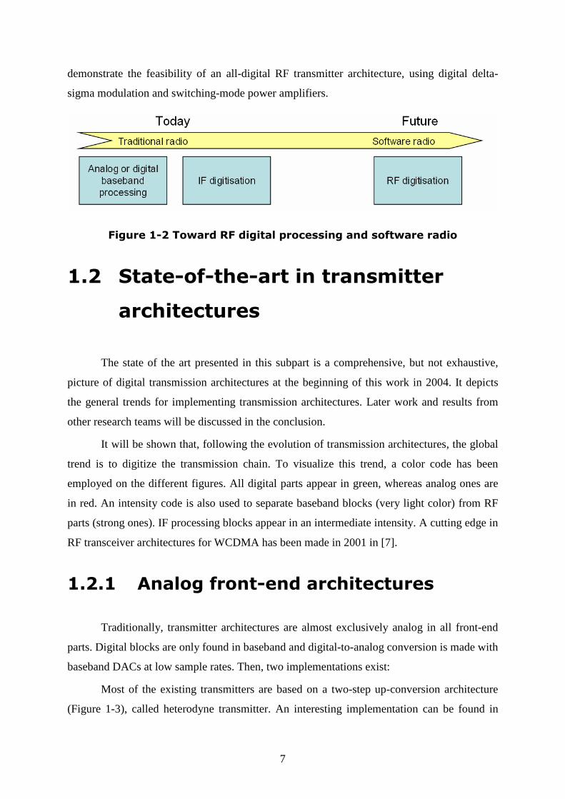
Figure 1-2 Toward RF digital processing and software radio
1.2 State-of-the-art in transmitter
architectures
The state of the art presented in this subpart is a comprehensive, but not exhaustive,
picture of digital transmission architectures at the beginning of this work in 2004. It depicts
the general trends for implementing transmission architectures. Later work and results from
other research teams will be discussed in the conclusion.
It will be shown that, following the evolution of transmission architectures, the global
trend is to digitize the transmission chain. To visualize this trend, a color code has been
employed on the different figures. All digital parts appear in green, whereas analog ones are
in red. An intensity code is also used to separate baseband blocks (very light color) from RF
parts (strong ones). IF processing blocks appear in an intermediate intensity. A cutting edge in
RF transceiver architectures for WCDMA has been made in 2001 in [7].
1.2.1 Analog front-end architectures
Traditionally, transmitter architectures are almost exclusively analog in all front-end
parts. Digital blocks are only found in baseband and digital-to-analog conversion is made with
baseband DACs at low sample rates. Then, two implementations exist:
Most of the existing transmitters are based on a two-step up-conversion architecture
(Figure 1-3), called heterodyne transmitter. An interesting implementation can be found in
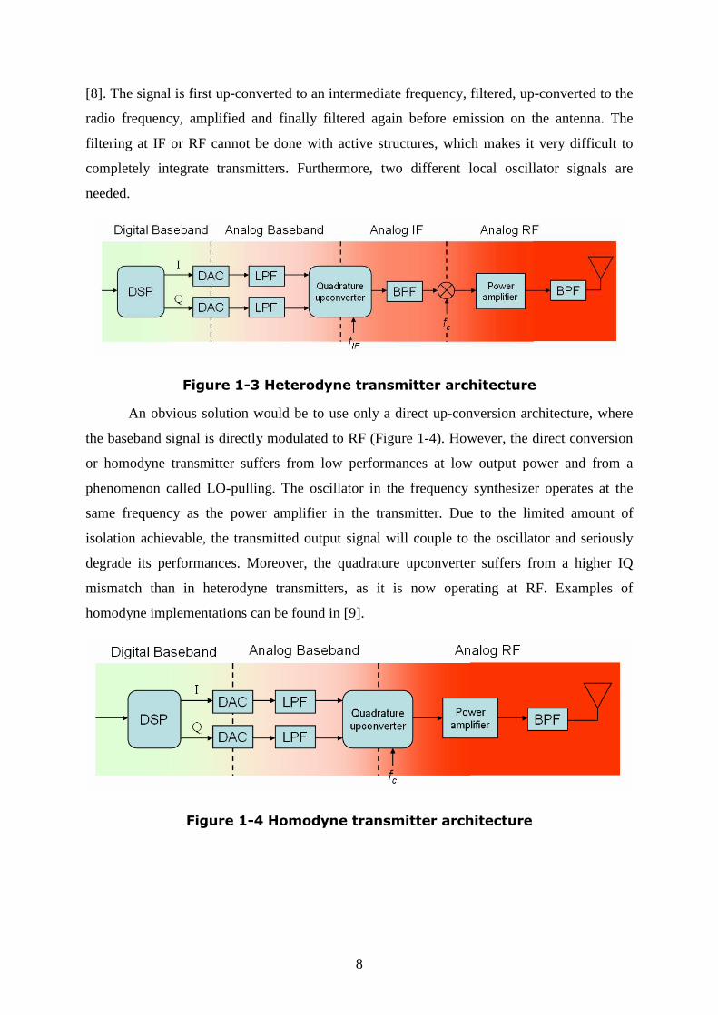
8
[8]. The signal is first up-converted to an intermediate frequency, filtered, up-converted to the
radio frequency, amplified and finally filtered again before emission on the antenna. The
filtering at IF or RF cannot be done with active structures, which makes it very difficult to
completely integrate transmitters. Furthermore, two different local oscillator signals are
needed.
Figure 1-3 Heterodyne transmitter architecture
An obvious solution would be to use only a direct up-conversion architecture, where
the baseband signal is directly modulated to RF (Figure 1-4). However, the direct conversion
or homodyne transmitter suffers from low performances at low output power and from a
phenomenon called LO-pulling. The oscillator in the frequency synthesizer operates at the
same frequency as the power amplifier in the transmitter. Due to the limited amount of
isolation achievable, the transmitted output signal will couple to the oscillator and seriously
degrade its performances. Moreover, the quadrature upconverter suffers from a higher IQ
mismatch than in heterodyne transmitters, as it is now operating at RF. Examples of
homodyne implementations can be found in [9].
Figure 1-4 Homodyne transmitter architecture

9
1.2.2 Digital IF architectures
Figure 1-5 Digital-IF transmitter architecture
An evolution from previous implementations is the Digital-IF architecture, in which
the digital signal is converted to analog after IF quadrature upconversion, generally using a
∆Σ DAC (Figure 1-5). This architecture benefits from better silicon integration, ideal IQ
matching and thus a lower error vector magnitude.
An interesting implementation is presented in [10] and [11], which details a digital
quadrature modulator, associated with a 1-bit ∆Σ modulator and a current-mode DAC to
replace analog IF upconversion (Figure 1-6). The 0.13µm CMOS chip can work with a
700MHz clock frequency to address an IF frequency of 175MHz. It consumes 139mW at
1.5V and occupies 5.2mm².
Figure 1-6 Digital quadrature modulator from [10]
In [12], this kind of architecture is implemented using a second-order-hold DAC in
0.25µm SiGe BiCMOS (Figure 1-7). The multi-bit delta-sigma DAC is working at 250MHz.
Analog Variable Gain Amplifier (VGA) and mixer stages are integrated into the chip to
deliver an output power of 5dBm, while consuming 180mW at 3V. However, this structure is
working with current-mode DACs, which limits, at low voltage, the maximum power that can

10
be delivered to a load. Such structures are incompatible with more efficient class-S power
amplification.
Figure 1-7 Conceptual block diagram of the digital-IF heterodyne transmitter from [12]
1.2.3 Digital RF architectures
Figure 1-8 Digital RF transmitter chain
Advances and maturity of deep submicron CMOS technologies enable the DAC to
reach higher sample rates. So, the idea of a digital RF implementation is rising [4, 5, 13] . It
deletes all analog mixers and replaces them by a direct-digital quadrature upconverter and a
switching-mode power amplifier driven by, e.g., a ∆Σ-modulated high-speed signal (Figure
1-8 and Figure 1-9). An advantage is the high efficiency of the output stages. At the time of
this work, no IC implementation of this kind of structures can be reported. However, ideas for
such architectures are presented in several publications.

11
Figure 1-9 DSP-based wireless transmitter architecture from [5]
The fundamental concept is to use bandpass ∆Σ modulation to produce a high-speed
digital signal driving a switching PA:
• [14] demonstrates such a digital transmission chain by experimentally
generating the produced bit-stream with a pattern generator and a serializer.
• [6, 15-17] present the concept and show simulation and measurement results
for relatively low output frequency, extrapolating simulations to higher output
frequencies.
Another method for digitally generating an RF signal is termed “Quadrature Integral
Noise Shaping” (INS) and uses PWM coding scheme to generate baseband IQ complex
signals. References [18] and [19] detail related architectures.
Moreover, an interesting paper [20] proposes to drive a DCO (Digitally Controlled
Oscillator) with a ∆Σ-modulated signal to generate the phase information and to regulate the
power amplifier amplitude to control the amplitude information.
Digital generation of RF signals by ∆Σ modulation and switched power amplifiers
seems to be the most promising implementation in terms of configuration possibility and
software radio convergence.
1.3 UMTS standard specifications
The Universal Mobile Telecommunications System (UMTS) in Frequency Division
Duplex (FDD) mode will be first considered in order to emphasize the concept studied in this
work. UMTS is the standard chosen for 3G mobile communications in Europe. Specifications
for the UMTS standard are defined by ETSI [21]. These specifications cover all aspects of

12
transmission and reception for handset terminals. As an introduction to UMTS, only aspects
that concern the definition of the global transmitter to be designed are given hereafter.
Furthermore, the extension of the highlighted approach to other standards is still under
investigation and will be discussed in the conclusion.
1.3.1 Introduction to UMTS
1.3.1.1 Protocol layers
The architecture of the UMTS radio interface is structured into layers, in which
protocols are based on the first three layers of the Open Systems Interconnection (OSI)
reference model [22], as illustrated in Figure 1-10:
• The first layer is the physical one, devoted to transmit and receive data over the
channel.
• The second layer is the medium access control (MAC), which is able to control
the data sent and received and to retransmit error packets. This layer provides
data and information to the physical layer.
• The third layer is the radio resource control (RRC). It controls and maps the
connections.
Figure 1-10 Radio interface protocol structure [22]

13
In the following sections, only transmitter physical layer, starting from the baseband
signals provided by the MAC layer will be considered.
1.3.1.2 Access mode and frequency
allocation
The frequency sharing technique adopted for UMTS is the Code Division Multiple
Access (CDMA): data from different users coexist within the same channel and spread
spectrum modulation is used to attribute a specific code to each user. Two methods allow
spreading signals: the Frequency Hopping (FH-SS) technique and the Direct-Sequence one
(DS-SS) [23]. Since only the DS-SS technique is adopted in UMTS, it is shortly detailed
hereafter. Direct-Sequence spread spectrum consists in multiplying the signals symbols by a
specific pseudo-random binary sequence. CDMA systems using direct sequence spreading are
called DS-CDMA. For UMTS, information is spread over about 5MHz, hence it is called
WCDMA (W is for Wideband). Two duplex modes exist in UMTS, Frequency Division
Duplex (FDD) and Time Division Duplex (TDD).
Figure 1-11 gives a comparison between spectrum access techniques used in GSM and
UMTS. For GSM, the whole frequency band is split into 200kHz wide channels multiplexed
in time between emission and reception. For UMTS in TDD mode, information is spread over
5MHz channels and separated per code. The transmitter and the receiver are working in half-
duplex. Time slots are alternatively allocated for emission and reception. FDD mode also uses
CDMA but the transceiver is working in full-duplex. The reception band is placed away from
the emission band (not shown in the figure). The two front-end architectures operate at the
same time, using a duplexer.

14
Figure 1-11 Examples of access modes for GSM, UMTS TDD and FDD
The study is focused on FDD mode in which uplink and downlink are separated in two
frequency bands, instead of separated time slots. UMTS FDD operates on two 60MHz bands,
separated by 190MHz. The uplink uses 1920-1980MHz band while the downlink band is
located between 2110 and 2170MHz. Our interest only goes to the uplink path, from the user
terminal to the base station.
Inside the 1920-1980MHz band, twelve 5MHz wide channels exist. Chip rate is
3.84Mc/s (Mega chips/second), but data rate is tied to the spreading factor. Channels are
larger than the relative chip rate due to the roll-off factor (generally stated α) of the Root-
Raised Cosine (RRC) filter used. In UMTS, the roll-off factor is equal to 0.22, thus the
channel bandwidth is equal to chip rate =+× )1( α 4.68MHz. A channel is shown on Figure
1-12, illustrating the effect of the root-raised cosine filter. The modulation used by UMTS is
the Quaternary Phase Shift Keying (QPSK).

15
Figure 1-12 Example of a RRC-shaped UMTS channel
1.3.2 UMTS specifications for transmitters
Specifications on spectrum emissions are given at the antenna connector. It will be
considered that the antenna connector is loaded by a nominal single ended 50 Ω impedance.
These specifications lead to a spectrum emission mask and out-of-band spurious emissions
constraints as explained in the following sections.
1.3.2.1 Spectrum emission mask
The spectrum emission mask applies to frequencies, which are between 2.5 MHz and
12.5 MHz away from the User Equipment (UE) centre carrier frequency (related to the chosen
channel). The out-of-channel emission is specified relative to the RRC filtered mean power of
the UE carrier. Table 1-1 shows requirements for UMTS spectrum emission mask and Figure
1-13 translates the requirements on a graph.

16
Relative requirementAbsolute
requirement
2.5 ≤ ∆f ≤ 3.5 MHz -71,1 dBm 30 kHz
3.5 ≤ ∆f ≤ 7.5 MHz
7.5 ≤ ∆f ≤ 8.5 MHz
8.5 ≤ ∆f ≤ 12.5 MHz -49 dBc
Note 2: The minimum requirement is calculated from the relative requirement or the absolute requirement, whichever is the higher power.
Minimum requirement (Note 2)Measurement
bandwidth
-55,8 dBm 1 MHz
∆f in MHz (Note 1)
Note 1: ∆f is the separation between the carrier frequency and the center of the measurement bandwidth.
dBc5.2MHz
f1535
−∆−−
dBc5.3MHz
f135
−∆−−
dBc5.7MHz
f1039
−∆−−
Table 1-1 UMTS spectrum emission mask
Figure 1-13 UMTS spectrum emission mask (related to a 1MHz measurement bandwidth)
1.3.2.2 Adjacent Channel Leakage Power
Ratio
Another parameter is defined to obtain the desired spectrum requirement. Adjacent
Channel Leakage power Ratio (ACLR) is the ratio of the RRC filtered mean power centered
on the assigned channel frequency to the RRC filtered mean power centered on an adjacent
channel frequency. If the channel power is greater than -50dBm then the ACLR specifications
in Table 1-2 should be met.

17
Table 1-2 UMTS ACLR
1.3.2.3 Spurious emissions
In addition to in-band requirements, UEs are not authorized to spread power
everywhere. Some frequency bands, used in other standards, are sensitive to perturbations. To
overcome this, maximum spurious emission levels are defined in determined frequency
bands. Out-of-band requirements are plotted on Figure 1-14 between 900MHz and 2.2GHz.
This plot corresponds to normalized power emission in dBm/Hz over standards frequency
bands, as defined by the ETSI (Table 1-3). On this qualitative plot, proportionality is not
respected. However, this plot is relevant for visual understanding.
Receive band specifications (RX bands) are the hardest ones to meet. For the GSM900
band, a maximum of -129dBm/Hz is required. For the DCS1800, -126dBm/Hz is the limit of
spurious emission. The RX band of UMTS is placed 190MHz higher than transmit band (TX
band). The maximum allowed level is -129dBm/Hz at the antenna. However, an UMTS
terminal is working in full duplex using a duplexer. That means the UE is transmitting and
receiving data at the same time. That’s the reason why the RX band requirement must be
lowered down to -183dBm/Hz. UMTS RX and DCS1800 RX specifications are the most
demanding ones, as they are very close to the UMTS transmit band (TX band).

18
Figure 1-14 UMTS spurious requirements
Measurement Bandwidth Requirement (dBm)0,009 - 0,15 1 kHz0,15 - 30 10 kHz
30 - 860 100 kHz860 - 895 3.84 MHz -60895 - 921 100 kHz -36921 - 925 100 kHz -60925 - 935 3.84MHz -60935 - 960 100 kHz -79960 - 1000 100 kHz -36
1000 - 1805 1 MHz -301805 - 1844,9 100 kHz -71
1844,9 - 1880 3.84 MHz -601880 - 1884,5 1 MHz -30
1884,5 - 1919,6 300 kHz -411919,6 - 2110 1 MHz -30
2110 - 2170 3.84 MHz -602170 - 2620 1 MHz -302620 - 2690 3.84 MHz -602690 - 12750 1 MHz -30
Frequency Band (MHz)
-36
Table 1-3 UMTS spurious emissions table
1.3.2.4 Error Vector Magnitude
Finally, UMTS norm defines quality criterions. A useful one is the Error Vector
Magnitude (EVM) measurement. It is an evaluation of the difference between a reference data
signal and the measured data signal. EVM is defined as the square root of the ratio between

19
the error vector mean power and the reference signal mean power, expressed in percentage.
Figure 1-15 explains on an IQ diagram the phase and amplitude errors associated with the
EVM definition. In normal conditions and for an output power greater than -20dBm, EVM
must be lower than 17.5%. However, typical performance of mobile transmitters is an EVM
of about 7%.
Figure 1-15 Amplitude and phase errors defining EVM
1.4 Conclusion
The work presented in this thesis is devoted to software radio, trying to approach as
much as possible an ideal implementation. In a first study, the European standard for 3G
communications (UMTS) is chosen for its hard-to-fulfill requirements. Main UMTS
specifications, directly related to our work, have been detailed.
Nowadays, transmitters in mobile handsets are mainly analog. The trend to digitize all
processing blocks brings us to find new ways of implementing transmission chains. An
architecture based on digital RF ∆Σ modulators, digital quadrature upconverters and
switching-mode power amplifiers has been determined as a good candidate to enable digital
radio and will be discussed in more detail in the next chapter.


21
CHAPTER 2
DIGITAL TRANSMITTER
ARCHITECTURE
The digital RF transmitter architecture, as presented in paragraph 1.2.3, can be
implemented, at system level, in several different ways. In the first section of this chapter, two
possible system architectures are presented and the choices made in this work justified. The
more detailed structure of all sub-blocks in the selected system architecture is presented in the
subsequent sections.
2.1 Global transmitter architecture
2.1.1 Transmitter architecture and
frequency planning
Figure 2-1 Digital transmitter architecture. chipf is the chip rate, cf the
carrier frequency and sf the sampling frequency.
The global function of the digital transmitter is to convert a multi-bit digital I/Q
baseband signal at baseband sampling rate (chip rate) into a digital 1-bit RF signal at a very

22
high sampling rate that can be fed to a switching power amplifier. The underlying
fundamental principles are oversampling and noise-shaping. Delta-sigma modulators are used
to shape the noise in an appropriate way to move it out of the targeted transmit band. The
global architecture is presented on Figure 2-1. An analog filter is then necessary at the output
of the digital transmitter to remove the high out-of-band quantization noise. If a fixed
frequency analog filter is used, the modulator must provide low quantization noise over the
full transmit band of the targeted standard for all carrier frequencies. In a simple direct-
conversion architecture, the sampling frequency would be proportional to the carrier
frequency. The worst-case situations are then the channels situated at the edges of the transmit
band (Figure 2-2a). In fact, for a low quantization noise for all possible channels inside the
standard band, the ∆Σ modulator bandwidth must be twice the width of the transmit band,
thus increasing the noise shaper requirements.
Figure 2-2 Modulator output spectrum for channels at the lowest band edge for (a) direct conversion and (b) two-step conversion
To relax the requirements on the noise shaper, a two-step upconversion architecture
has been chosen (Figure 2-3). The RF sampling frequency is fixed, and the center of the
noise-shaper bandwidth is placed on the center of the standard transmit band, independently
of the actual channel used for the transmit path (Figure 2-2b). In the first step the complex
base-band signal is moderately oversampled and then placed on the appropriate channel by a

23
digital multiplier. For UMTS, the corresponding 12 channel center frequencies are stated in
Table 2-1 and are given by:
( ) 5,4,3,2,1,0,55.2 =×+±= kMHzkMHzFchannel Eq. 2-1
Figure 2-3 Two-step upconversion transmitter architecture. L is a factor dependent over the chosen standard.
Channel number Channel center frequency
1 -27.5 MHz
2 -22.5 MHz
3 -17.5 MHz
4 -12.5 MHz
5 -7.5 MHz
6 -2.5 MHz
7 2.5 MHz
8 7.5 MHz
9 12.5 MHz
10 17.5 MHz
11 22.5 MHz
12 27.5 MHz
Table 2-1 Channel center frequencies for UMTS standard
In the second step the signal is again oversampled up to the RF sampling frequency,
transposed to RF and finally quantized with a bandpass 1-bit noise-shaper.
Upconversion of the digital IF signal to RF is achieved by a digital image-reject mixer
as shown in Figure 2-3. In the general case, two multipliers and a summer are required, all
operating at the RF sampling frequency. By choosing the RF sampling frequency equal to 4
times the center frequency of the transmit band, the operation is however greatly simplified.
In that case, the 90° phase shifted I and Q Local Oscillator (LO) signals can be represented by
the following sequences [24]:

24
LOI : 1, 0, -1, 0
LOQ : 0, 1, 0, -1
As it can be seen, at any time one of the two LO signals is equal to zero. Therefore, the
adder in the mixer can be replaced by a simple multiplexer, selecting the I channel on odd
periods and the Q channel on even periods. Furthermore, the multiplications are replaced by a
simple change of the sign of the digital data, eliminating multipliers entirely. The digital
image-reject mixer reduces to the function shown in Figure 2-4. The digital RF output stream
is simply the following sequence:
,...12,8,4,0,)3(),2(),1(),( =+−+−+= nnQnInQnIRFout Eq. 2-2
Figure 2-4 Digital mixer operation. The sample rate is cf×4 and
,...12,8,4,0=n
A major drawback of this architecture is however the fact that the ratio of the IF to the
RF sampling frequencies is not necessarily integer, as one is related to the chip rate and the
other to the center frequency of the standards transmit band. A sophisticated multi-rate digital
interpolator is in principle necessary to accomplish this sample-rate conversion. This can
however be avoided through careful frequency planning. By slightly offsetting the RF
sampling frequency, an integer ratio can be reached. The corresponding frequency offset on
the channel center frequency must simply be corrected in digital baseband by offsetting the
channel center frequencies by the opposite amount. In the case of UMTS, the chip rate is
3.84MHz, while the exact center frequency is 1950MHz, yielding a ratio of 507,8125. As an
example, when setting the RF center frequency to 512 times the chip rate, it is offseted by
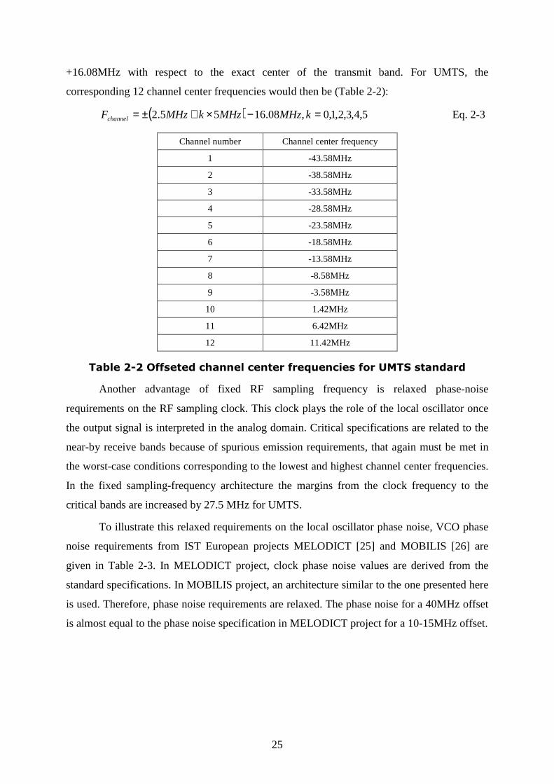
25
+16.08MHz with respect to the exact center of the transmit band. For UMTS, the
corresponding 12 channel center frequencies would then be (Table 2-2):
( ) 5,4,3,2,1,0,08.1655.2 =−×+±= kMHzMHzkMHzFchannel Eq. 2-3
Channel number Channel center frequency
1 -43.58MHz
2 -38.58MHz
3 -33.58MHz
4 -28.58MHz
5 -23.58MHz
6 -18.58MHz
7 -13.58MHz
8 -8.58MHz
9 -3.58MHz
10 1.42MHz
11 6.42MHz
12 11.42MHz
Table 2-2 Offseted channel center frequencies for UMTS standard
Another advantage of fixed RF sampling frequency is relaxed phase-noise
requirements on the RF sampling clock. This clock plays the role of the local oscillator once
the output signal is interpreted in the analog domain. Critical specifications are related to the
near-by receive bands because of spurious emission requirements, that again must be met in
the worst-case conditions corresponding to the lowest and highest channel center frequencies.
In the fixed sampling-frequency architecture the margins from the clock frequency to the
critical bands are increased by 27.5 MHz for UMTS.
To illustrate this relaxed requirements on the local oscillator phase noise, VCO phase
noise requirements from IST European projects MELODICT [25] and MOBILIS [26] are
given in Table 2-3. In MELODICT project, clock phase noise values are derived from the
standard specifications. In MOBILIS project, an architecture similar to the one presented here
is used. Therefore, phase noise requirements are relaxed. The phase noise for a 40MHz offset
is almost equal to the phase noise specification in MELODICT project for a 10-15MHz offset.

26
Offset (MHz) Phase noise level in MELODICT project
Phase noise level in MOBILIS project
5 -99.2dBc/Hz -
10 -117dBc/Hz -
15 -120dBc/Hz -
40 -148dBc/Hz -119dBc/Hz
Table 2-3 RF clock frequency phase noise requirements
2.1.2 Digital upconversion and noise-
shaping architecture
Two architectures can achieve the required functions of quantizing the input signal to
a 1-bit data stream and upconvert the baseband signal to the desired RF band. These
architectures are presented on Figure 2-5. In the first one, a bandpass ∆Σ modulator clocked at
cf×4 is placed after the digital up-conversion to produce the 1-bit digital output stream. In
the second one, two lowpass ∆Σ modulators, also clocked at cf×4 , are placed on I and Q
paths prior to the upconversion of the signal [27].
Figure 2-5 Possible architectures for noise shaper and upconverter: a) Bandpass ∆Σ modulator; b) Lowpass ∆Σ modulators.

27
In terms of complexity, the two architectures are approximately equivalent. The digital
mixer is simpler in the second architecture, as it operates only on 1-bit signals. The
complexity of the ∆Σ modulators is equivalent, as the order of the bandpass ∆Σ modulator is
twice the order of the low-pass ∆Σ modulators for the same noise-shaping at the output.
However, the second architecture offers further margins for optimization. If we further refine
the analysis, it can be noticed that the input of the digital I/Q mixer actually samples only odd
samples in I path and only even samples in Q path. If we do not produce the unnecessary
samples, the effective sampling rate of the delta-sigma modulators in I and Q paths is only
half of the RF sampling rate (Figure 2-6). The ∆Σ modulators are working in quadrature for
proper operation. This will not only halve the power consumption of the modulators but also
relax the requirements on the digital logic in the modulators as the cycle time is doubled. The
combination of these two effects obviously is in favour of the second architecture, which
clearly seems to be superior to the bandpass approach.
Figure 2-6 Simplified architecture if only one sample on two is computed
inside the ∆Σ modulators. The ∆T delay is equal to cf41 .

28
Figure 2-7 Frequency spectrum of the output of the digital upconverter when no interpolation is done on Q channel, showing the image that
appears
Figure 2-8 Architecture if the ∆Σ modulators sampling clocks are synchronous.
In practice, however, we would like to use the same sampling instants for the two low-
pass ∆Σ modulators in I and Q paths. If we simply process only odd samples in both I and Q
paths, an image of the transmit channel appears in the RF spectrum because of the slight
phase shift of the Q path (Figure 2-7). This can be solved in two ways. In a rigorous approach,

29
the odd samples of the I path are delayed by one RF clock period, so that they now appear on
the same clock edges as the even samples of the Q path (Figure 2-8).
Figure 2-9 Chosen architecture using a linear interpolation on Q channel.
∆T’ delay is equal to cf21 .
The drawback is that it is still necessary to oversample and interpolate the input
signals to the RF sampling rate. An alternative approach is to linearly interpolate only the
missing even Q samples from the odd ones. This globally reduces the sampling rate for all the
circuitry prior to the digital mixer. The corresponding architecture and the effective image
suppression in the RF spectrum are shown in Figure 2-9 and Figure 2-10.

30
Figure 2-10 Digital upconverter output spectrum. 8th channel is chosen. 0dBFS refers to a full-scale sine wave.
2.1.3 Power amplifier and antenna filters
Output stages are not the main purpose of this work, but understanding of these blocks
is essential in order to clarify implementation issues and to be aware of non-idealities and
trade-offs to overcome. This part will focus on these issues.
The power amplifier, associated with antenna filters, is actually a 1-bit power digital-
to-analog converter (DAC) [6, 15]. An advantage is the high linearity provided by the
amplifier, as only two states exist. Switched-mode (class S) power amplifiers are also known
to have a good theoretical efficiency.
2.1.3.1 Switching-mode power amplifier
topology
The simplest switched-mode power amplifier is a simple inverter, large enough to
provide the desired power, while working in triode region. Obviously, a growing chain of

31
inverters must be implemented, to be able to drive the last one. Let’s only consider the last
inverter, presented on Figure 2-11. Theoretically, the efficiency is 100% when an ideal filter
is inserted between the inverter and the load. All consumed power is directly provided to the
load. Unfortunately, many losses degrade efficiency. Hence, total power is divided into useful
load power, dissipated power in linear drain-to-source on-resistance, switching losses and
direct path losses during transitions [28].
Figure 2-11 On the left, schematic of the output inverter; on the right, a diagram showing the repartition of the power supply
First, the RDS on-resistance (in linear region) dissipates power as it acts as a resistive
divider with Rload. RDS is inversely proportional to the width W of the transistors. Next,
switching losses are dependent of the value of Cout, proportional to W and the switching
frequency. It is to note that in most cases, Cout will be overcome by be next driven gates or by
the wiring capacitance (if the inverter is directly connected to a bonding pad, for example).
Finally, during transitions, current is flowing directly from VDD to ground, leading to direct
path losses. Let’s call trf the mean transition time for rise and fall, the direct path losses are
frequency dependant and express as ftIV rfpeakdd ... .
For high frequency activity, wasted power would become very large. Thus, there is a
trade-off to make, when sizing the inverters, between staying in triode region to deliver the
right current and voltage to the load and reducing the parasitic power consumption.
Another aspect to take into account when dealing with the output stages efficiency is
the consumption of the inverter chain driving the last inverter. This consumption is process
dependent, as it determines the number and the sizes of preceding stages.
Moreover, in the kind of architecture developed here, the useful information is band-
limited, so the square wave output of the power amplifier contains sinusoidal-shaped data in a
band situated around the fourth of its sample rate. Thus, taking a sine wave example, the

32
power contained by the useful information is 3dB lower than the power of the total square
wave (holding all other frequencies). If we define the total efficiency as the ratio of the useful
data power to the total consumed power, then this total efficiency falls down to 50%. A
solution to avoid the amplification of unwanted frequencies, and so the associated useless
consumption, is to design a filtering stage between the inverter output and the load. Filters
must be wide enough not to distort content and sharp enough to correctly remove unwanted
noise.
2.1.3.2 Power DAC non-idealities
The power amplifier is the limit between digital and analog world. Although it works
on a single digital bit, it converts code information into an analog voltage representation.
That’s why we called it a power DAC. Inter-symbol interference (ISI) is the major distortion
brought by the conversion. It comes from three major contributions.
First of all, the rise and fall times of the transitions will introduce a change in the
energy contained in the signal. Figure 2-12a shows the effect of rise and fall times on the
signal. For example, x2, x4 and x5 have the same logic value but different energies because of
the next sample polarity. This difference doesn’t appear with ideal edges. Study of this effect
shows no alteration of the signal spectrum shape [29].
Figure 2-12 Inter-symbol interference: a) with symmetric fronts; b) with asymmetric fronts
The second effect is the edges asymmetry (Figure 2-12b). This study and other works
explain that ISI is not created by rise and fall times, but by the unbalanced positive and
negative symbols [30]. This asymmetry greatly degrades the frequency response by increasing

33
noise inside the bandwidth. Symmetry can be realized by using differential architectures. A
comparison is shown in Figure 2-13, illustrating the benefit of a differential structure.
Differential implementation deletes all ISI coming from this phenomenon and also offers the
advantage of doubling the signal swing, thus quadrupling the output power. It obviously goes
with more complex design and a larger silicon area.
Figure 2-13 Output spectra for ideal, single-ended and differential outputs
Finally, the last contribution is the jitter, defined as a misplacement of the edges
related to the ideal sampling instant. Total jitter is decomposed in periodic jitter (also called
sinusoidal jitter), caused by external deterministic noise sources, like switching power-supply
noise, and in random jitter. Jitter increases the noise floor inside the bandwidth of interest. It
mainly comes from clock oscillator phase noise.

34
Figure 2-14 Example of ACLR variations, for 5 and 10 MHz offset channels, related to random jitter variance.
An example of a random jitter study is presented in Figure 2-14, coming from an
internal report on jitter study [31]. The ACLR requirements for UMTS, as stated in first
chapter, are 33dB and 43dB for 5 and 10MHz offsets, respectively. Some headroom has been
added so that the ACLR specification is set to 50dB. ACLR versus random jitter variance has
been plotted to determine the maximum allowable jitter to reach the requirements. Here, the
maximum jitter variance is 1.9ps to keep an ACLR greater than 50dB for both specifications.
2.1.3.3 Antenna filters
An issue in this kind of architecture using digital ∆Σ modulators is the resulting
quantization noise outside the band of interest. This noise must be removed, especially in the
frequency bands where other standards are operating. These constraints have been presented
in the first chapter. The Figure 2-15 presents the system output digital spectrum, trasnposed to
the antenna, if no filtering is done, to illustrate the demands in terms of filtering.
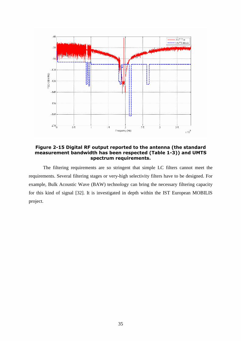
35
Figure 2-15 Digital RF output reported to the antenna (the standard measurement bandwidth has been respected (Table 1-3)) and UMTS
spectrum requirements.
The filtering requirements are so stringent that simple LC filters cannot meet the
requirements. Several filtering stages or very-high selectivity filters have to be designed. For
example, Bulk Acoustic Wave (BAW) technology can bring the necessary filtering capacity
for this kind of signal [32]. It is investigated in depth within the IST European MOBILIS
project.

36
2.2 UMTS implementation case of the
digital transmitter
2.2.1 Proposed digital transmission chain
Figure 2-16 Proposed transmitter chain
Figure 2-16 depicts the block diagram of the complete digital RF signal generator
architecture considered throughout the rest of this work [33]. The delta-sigma (∆Σ)
modulators and the digital upconverter provide a very high-speed 1-bit stream containing all
in-band information. The oversampled ∆Σ modulators aim at keeping a high dynamic range
within the bandwidth, and simultaneously at shaping the noise outside the band of interest.
Since this block works with an oversampled signal, the signal from the baseband processing is
upsampled to reach the ∆Σ modulators’ sample rate.
This architecture tends towards an ideal software radio implementation by processing
digital signals as close as possible to the antenna.
The following sections describe in details each block along the transmitter chain for
the case of a UMTS implementation (except for the last three blocks, detailed earlier).
2.2.2 Baseband processing
The study of these blocks helps us in characterizing the system input signal. Indeed, a
prior knowledge about information processed through the whole transmission chain is
required before any simulation. The desired signal is an IQ modulated complex signal. Digital

37
processing blocks ensure its shaping [34, 35]. Figure 2-17 shows baseband blocks, while
Figure 2-18 highlights the successive steps, depicted by encircled numbers, for generating the
baseband signal.
Figure 2-17 Baseband processing blocks
First of all, two input signals called DPDCH and DPCCH (for Dedicated Physical
Data Channel and Dedicated Physical Control Channel) contain information to transmit. It
can be voice as well as communication data of any type. For generation purpose, these signals
have been generated as pseudo-random binary sequences and then multiplied by orthogonal
codes obtained by Walsh method. Orthogonal codes are useful to spread the signal spectrum
over the desired bandwidth. At the output of this block, the binary sequences are sampled at
the 3.84MS/s UMTS chip rate
Then, data scrambling allows separating users by assigning each one a different code
and thus controls confidentiality of transmitted data [36]. PN-codes are used in UMTS to
generate the HPSK complex scrambling sequence [37, 38].
Root-raised cosine (RRC) filtering is used to limit the spectrum of the coded
information and to provide a properly shaped signal with preservation of its content.
Moreover, inter-symbol interference is reduced by a filter such as a Nyquist filter. This digital
filter enlarges the 3.84MHz signal with the 0.22 roll-off factor in order to have a 5MHz
channel. It also introduces a delay equivalent to the half of the filter length. The output sample
rate is twice the chip rate and equals 7.68MS/s.

38
Figure 2-18 Baseband signals at each step of the baseband processing
The proposed transmitter will compute the whole standard band (i.e. 60 MHz), instead
of only a 5MHz wide shaped channel. Thereby, the 5MHz channel has to be placed, during
baseband processing, on a chosen channel among the 12 available ones. It is done by
oversampling stages followed by a CORDIC algorithm (Coordinate Rotation Digital
Computing) [39]. In our case, the signal is oversampled 16 times to reach 122.88MS/s. This
sample rate is chosen in order to avoid aliasing images of the channel from being too close to
the channel of interest. That would not be acceptable for proper filtering of those images. The
122.88MS/s sample rate ensures images to fold relatively far away from the signal band.
The CORDIC rotator is a digital implementation of an upconverter, using exclusively
adders and barrel shifters. CORDIC algorithm digitally places the channel on the appropriate
IF carrier. Each channel is defined by a number i (from 1 to 12) and an associated centre
frequency fi which is a multiple of 2.5MHz situated between -30 and +30MHz plus or minus
an offset corresponding to Table 2-2. Given the desired channel frequency, CORDIC
algorithm is able to place the channel around this carrier with relatively low complexity.
All these baseband blocks have been modeled using MATLAB software to produce a
flexible generation tool for further transmitter simulations. An example of a baseband output

39
signal is presented in Figure 2-19. The 9th channel, situated between 10 and 15MHz, is chosen
here as an example.
Figure 2-19 Spectrum of the IQ baseband output signal (9th channel is chosen arbitrarily). Amplitude is referred to 0dBFS (full-scale sine wave).
2.2.3 Sample rate conversion
In the architecture considered here, the 122.88MS/s IQ signal has to be oversampled to
3.9GS/s, which is twice the carrier frequency of UMTS standard, in order to feed the
oversampled delta-sigma modulator. The oversampling ratio is about 31.73. As explained
earlier, the ∆Σ modulators sampling frequency would be adjusted to 3.93216GS/s for the
oversampling ratio to be exactly 32. The channels would be offseted during baseband
processing, thus the operation could be achieved by several half-band filters in cascade. Good
image attenuation could be obtained but as sample rate increases, computational requirements
become huge.
Since the digital delta-sigma modulator produces quantization noise outside the band
of interest, non attenuated images by digital oversampling filters will fall below the
quantization noise. This will happen provided the images are rather far from the centre of the
band. Indeed, the quantization noise gets higher as frequency increases. It has been shown

40
that a first half-band filtering with more than -70dBc attenuation on 122.888MHz images
related to the channel power can relax requirements for other stages. Then, first-order
interpolation by 16 can easily be realized at very low cost. Images at multiples of 245.76MHz
never rise above the quantization noise. This is done by simply sample and hold the input
signal at 16 times its rate. Good filtering at low sample rate relaxes computational effort at
high sample rates. Figure 2-20 shows the chosen sample rate conversion architecture and
highlights intermediate sample rates.
Figure 2-20 Sample rate conversion blocks
Figure 2-21 illustrates the implementation and shows the output spectrum for different
configurations of data oversampling. The estimated delta-sigma modulator quantization noise
is also drawn to choose the best solution, with following parameters:
a) First-order interpolation by 32 (from 122.888MS/s to 3.9GS/s). One can notice that
the image at 122.88MHz rises above the quantization noise;
b) Half-band filtering followed by first-order interpolation by 16. This is a good
trade-off between complexity and image attenuation.
Figure 2-21 Spectrums of the 3.9GS/s SRC output signals for the two configurations previously cited. In red, the estimated shaped
quantization noise brought by the ∆Σ modulator.

41
2.2.4 Digital ∆Σ modulators
Interesting and detailed literature on oversampled delta-sigma modulation theory can
be found in [40-44].
2.2.4.1 Lowpass ∆Σ modulator architecture
The bandwidth of the designed lowpass modulators has been enlarged to 100MHz for
20MHz guard bands on both sides of the 60MHz transmit band. The corresponding
oversampling ratio is about 40. Lowpass ∆Σ blocks will be designed to fulfil the standard
requirements for in-band required dynamic range. Hence, a third-order modulator is designed,
with a 1-bit output data stream. It theoretically leads to approximately 80dB of maximum
SNR.
Figure 2-22 (a) Pole-zero diagram (pole: x; zero: o); (b) NTF (red) and STF (green) of the generated ∆Σ modulator (frequency is normalized to
fs=3.9GHz); (c) zoom on the bandwidth (fb=30MHz)
For architecture definition, we use the Delta-Sigma Schreier Toolbox for Matlab
software [45], which is a tool for automatically generating standard ∆Σ architectures with
optimal in-band zeros placement. A zero is centered at DC and the other ones are placed at the
limit of the bandwidth. This has the effect of flattening the noise transfer function (NTF)

42
inside the bandwidth. Hence, the adjacent noise power for each channel will be approximately
identical (Figure 2-22). It is to note that the signal transfer function (STF) introduces no in-
band attenuation.
The toolbox is able to translate the generated NTF and STF into a reliable architecture.
The chosen architecture type is a cascade of integrators with feedbacks that feed back the
quantized output to each integrator input. The configuration is presented on Figure 2-23. A
global feedback with the g1 coefficient creates the optimized zero location, at the limit of the
transmit band. Coefficients for this architecture are summed up in Table 2-4. The output
quantizer is working on two levels. Thus, it determines the sign of the computed signal. The
output spectrum of this two-level output signal is plotted on Figure 2-24.
Figure 2-23 Third-order ∆Σ modulator architecture
Coeffi-cient
Value Coeffi-cient
Value
a1 0.1409457518558072 c1 0.3166424812531309
a2 0.2435218988625833 c2 0.1684863887945898
a3 0.0945693329735421 g1 0.0219599951361829
b1 0.1409457518558072
Table 2-4 Coefficients for the 3rd-order ∆Σ modulator of Figure 2-23

43
Figure 2-24 ∆Σ modulator output spectrum
2.2.4.2 Simulated performances
For performance evaluation, we have considered classic parameters for ∆Σ
modulators. The main parameter is the Signal-to-Noise and Distortion Ratio (SNDR), which
is the SNR with distortion components (especially harmonics) taken into account as part of
the noise. Another one is the Spurious Free Dynamic Range (SFDR). It is the available
dynamic range between the maximum input power and the highest spurious power (most of
the time the 3rd harmonic).
For the above architecture we obtain dBSNDR 6.76= and dBSFDR 2.87= . The
former value leads to the calculation of an Effective Number Of Bits (ENOB) of 13, which is
the in-band dynamic associated with the calculated SNDR. These parameters are obtained by
putting a 10MHz sinusoidal signal at the input with the maximum stable amplitude (-3dBFS).
SNDR is relatively stable when applying sinusoids at other frequencies, due to the flatness of
the quantization noise.
When applying an UMTS channel-shaped signal, we have access to the Adjacent
Channel Leakage Ratio (ACLR) parameter for 5 and 10MHz offsets, which is the ratio
between the in-channel power to the respective leaked side-channel power. Since in our
specific architecture the side-channel power is mainly constituted by quantization noise, we
will consider through this thesis the Adjacent Channel Power Ratio (ACPR), which is ratio
between the in-channel power to the respective total side-channel power. We respectively

44
obtain 76.3 and 78.4dB. But this value can vary a little (<1dB), depending on the chosen
channel. Here, we choose the 8th channel for this simulation.
On Figure 2-25, the SNDR is plotted versus the input level referred to the quantizer. It
shows that the maximum stable input is -3dBFS and that the dynamic behavior of the
modulators is in agreement with the expected one.
Figure 2-25 Simulated SNDR for the ideal configuration
2.3 Conclusion
We have presented here an architecture for achieving digital RF generation, thus
enabling a digital radio. This architecture uses ∆Σ modulators to provide 1-bit high-speed data
streams containing all channels information, owing to their oversampling and noise-shaping
features. The ∆Σ modulator is the core of this system and its design is detailed in the next
chapter. Essential surrounding blocks, that ensure proper RF signal generation and ∆Σ
modulators functionality, have been described. Issues for the output power amplifier and
antenna filters have also been handled.

45
Besides ∆Σ modulators, key points of this architecture are the sample rate conversion
block, which oversamples the signal for proper ∆Σ modulation, and the digital upconverter,
that really creates the RF signal from the baseband oversampling ∆Σ-modulated digital signal.
UMTS standard has been chosen in order to dimension the system blocks.


47
CHAPTER 3
DELTA-SIGMA MODULATOR SYSTEM
DESIGN
This chapter will concentrate on the ∆Σ modulator system design. The previous
chapter explained the role of this block inside the transmission chain, dealing with
interconnections with surrounding blocks (sample rate conversion and digital upconversion).
From there, the required architecture for ∆Σ modulators has been defined. In this chapter,
physical implementation at high sample rate will be investigated, leading to the introduction
of different design concepts:
• The system architecture will be optimized to be suitable for a high-speed
digital implementation.
• The modulators’ coefficients will be scaled down to powers of two.
• The use of a redundant arithmetic scheme will reduce the length of the critical
path by enabling carry-free additions.
• Non-exact quantization of the output signal is used, because the carry
propagation issue has been transferred to the output quantizer.
• A precomputation of the quantization output is needed to parallelize the output
computations and reduce the critical path even more.
• Differential signals will be used everywhere inside the modulator core.
• Fast dynamic logic will be investigated.
The last two points will be detailed in the next chapter, dealing with circuit
considerations.

48
3.1 ∆Σ architecture optimization
The ∆Σ architecture needs further optimization given the high clock frequency
(3.9GHz for UMTS). The principal obstacles are the multipliers implementing the coefficients
in front of the adders. The architecture has been simplified by replacing all coefficients by
their closest power of two. This leads to the coefficient of Table 3-1. Multiplications simply
become right shifts (for negative powers of two) and can be implemented with little effort in
the routing scheme. No extra gates are then required to implement these operations.
Coeffi-cient
Value Implemented value
Coeffi-cient
Value Implemented value
a1 0.1409457518558072 2-3 c1 0.3166424812531309 2-2
a2 0.2435218988625833 2-2 c2 0.1684863887945898 2-3
a3 0.0945693329735421 2-3 g1 0.0219599951361829 2-5
b1 0.1409457518558072 2-3
Table 3-1 Power-of-two coefficients for the ∆Σ modulator
Figure 3-1 Third-order ∆Σ modulator architecture
Moreover, in the designed modulator of Figure 3-1, the accumulator, which is a zero-
delay integrator, would increase the longest path, thus limiting the maximum reachable clock
frequency. This path goes from the output of the third z1 block, through g1 feedback and
several adders, to the input of the same block. To reduce this path, the accumulator has been
changed into an integrator, according to the architecture in Figure 3-2 and simulated to
evaluate the degradation.

49
Figure 3-2 Optimized ∆Σ architecture. The accumulator has been replaced by an integrator.
Simulated performance obtained with this new architecture is not so much degraded,
considering the complexity reduction. Spectrally, the zeros are slightly shifted but they remain
close to the band limits. SNDR versus amplitude level is plotted on Figure 3-3. Maximum
SNDR is slightly reduced by about 3dB. Concerning ACLR for 5 and 10MHz offsets, the
simulation show maximum values of 74.7 and 72.2dB, respectively, for the maximum input
signal amplitude.
Figure 3-3 SNDR comparison for ideal and simplified architecture
In a digital implementation, signals are quantized, which is not taken into
consideration within the Matlab model. By contrast, VHDL simulations offer the possibility
to quantize the amplitude of processed signals. A VHDL model of the architecture has been
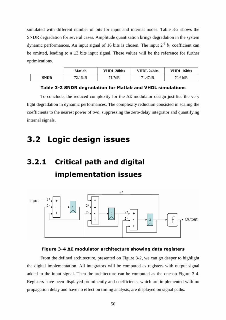
50
simulated with different number of bits for input and internal nodes. Table 3-2 shows the
SNDR degradation for several cases. Amplitude quantization brings degradation in the system
dynamic performances. An input signal of 16 bits is chosen. The input 2-3 b1 coefficient can
be omitted, leading to a 13 bits input signal. These values will be the reference for further
optimizations.
Matlab VHDL 28bits VHDL 24bits VHDL 16bits
SNDR 72.16dB 71.7dB 71.47dB 70.61dB
Table 3-2 SNDR degradation for Matlab and VHDL simulations
To conclude, the reduced complexity for the ∆Σ modulator design justifies the very
light degradation in dynamic performances. The complexity reduction consisted in scaling the
coefficients to the nearest power of two, suppressing the zero-delay integrator and quantifying
internal signals.
3.2 Logic design issues
3.2.1 Critical path and digital
implementation issues
Figure 3-4 ∆Σ modulator architecture showing data registers
From the defined architecture, presented on Figure 3-2, we can go deeper to highlight
the digital implementation. All integrators will be computed as registers with output signal
added to the input signal. Then the architecture can be computed as the one on Figure 3-4.
Registers have been displayed prominently and coefficients, which are implemented with no
propagation delay and have no effect on timing analysis, are displayed on signal paths.

51
Figure 3-5 Critical path
Timing analysis of this architecture highlights the critical path, constituted by the four-
input adder placed in front of the input of the second register. This critical path is detailed in
Figure 3-5. The quantizer provides a 1 bit output, so it works as an evaluation of the sign of
the input signal. In classical 2’s complement representation (C2), the sign is explicitly
handled by the Most Significant Bit (MSB). Thus, this quantizer does not introduce any
additional propagation delay.
Finally, critical path is essentially composed by adders, as in every other paths. The
most critical one comprises four 16-bit signals to add (or subtract). As it consists of a direct-
path signal and three feedback signals, the best optimization would be to compute the signals
two-by-two in parallel, leading to two consecutive 16-bit additions as shown on Figure 3-6. It
also makes the circuit insensitive to glitches, as the signal paths are matched.
Figure 3-6 Architecures for 4-inputs additions
Registers in the ∆Σ modulator are clocked at a 3.9GS/s rate. That means the period
between two clock edges is pssGS 4.256/9.31 = . For easier explanation in following
discussions, a 250ps period will be considered. This statement leads us to find a 16-bit adder
structure able to operate faster than a half clock period, i.e., 125ps. One can note that this
assumes ideal registers (no propagation delay and no setup time), which is surely not the case,
as it will be discussed later.
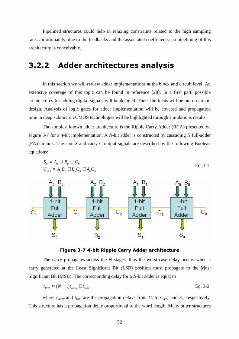
52
Pipelined structures could help in relaxing constraints related to the high sampling
rate. Unfortunately, due to the feedbacks and the associated coefficients, no pipelining of this
architecture is conceivable.
3.2.2 Adder architectures analysis
In this section we will review adder implementations at the block and circuit level. An
extensive coverage of this topic can be found in reference [28]. In a first part, possible
architectures for adding digital signals will be detailed. Then, the focus will be put on circuit
design. Analysis of logic gates for adder implementation will be covered and propagation
time in deep submicron CMOS technologies will be highlighted through simulations results.
The simplest known adder architecture is the Ripple Carry Adder (RCA) presented on
Figure 3-7 for a 4-bit implementation. A N-bit adder is constructed by cascading N full-adder
(FA) circuits. The sum S and carry C output signals are described by the following Boolean
equations:
nnnnnnn
nnnn
CACBBAC
CBAS
++=⊕⊕=
+1
Eq. 3-1
Figure 3-7 4-bit Ripple Carry Adder architecture
The carry propagates across the N stages, thus the worst-case delay occurs when a
carry generated at the Least Significant Bit (LSB) position must propagate to the Most
Significant Bit (MSB). The corresponding delay for a N-bit adder is equal to
sumcarryRCA ttNt +−≈ )1( , Eq. 3-2
where tcarry and tsum are the propagation delays from Cn to Cn+1 and Sn, respectively.
This structure has a propagation delay proportional to the word length. Many other structures

53
can help in reducing the dependency of propagation delay on the word length [46]. The
characteristics of the most popular structures are summarized in Table 3-3.
The Manchester Carry Chain (MCC) adder makes use of the well-known generate gn,
propagate pn and kill kn functions defined as:
nnn bag ⊕= , nnn bap ⋅= and nnn bak ⋅= Eq. 3-3
This structure does not reduce the worst-case propagation delay (when the carry
always propagates), but speeds up other cases. An implementation example can be found in
[47].
Carry SeLect (CSL) adder have a n propagation delay behavior. Two additions are
performed in parallel; one assuming the input carry is zero and the other assuming the input
carry is one. The decision is made when the carry is finally computed. An implementation
example can be found in [48].
Finally, the Carry LookAhead (CLA) adder is a powerful implementation due to its
nlog behavior. More circuitry is needed to estimate the carry for higher weight stages, but it
greatly speeds up the processing. It is the most widespread implementation for high-speed
adders [49].
Adder type Abbreviation Time Area
Ripple Carry Adder RCA O(n) O(n)
Manchester Carry Chain adder MCC O(n) O(n)
Carry SKip adder CSK O( n ) O(n)
Carry SeLect adder CSL O( n ) O(n)
Carry LookAhead adder CLA O( nlog ) O( nn log )
Signed-Digit Adder (base-r) SD-r O(b)* O(n)
Borrow and Carry-Save Adder CSA O(1) O(n)
*b is the number of bits per digit
Table 3-3 Time and Area requirements for most popular n-bits adders
Most of these architectures use two’s complement number system. Other number
representations, like Signed-Digit or Borrow-Save, lead to powerful adder implementations
with propagation delay independent of the word length.

54
3.2.3 Circuit level adders design
considerations
This section evaluates adder structures at the circuit level in order to identify
implementation issues and justify the architecture choice. The present study of full-adder
propagation delays structures has been made in STMicroelectronics 90nm CMOS technology.
The carry evaluation is the worst critical operation with respect to the global adder
speed. In a standard full-adder, carry evaluation needs three AND gates in parallel, followed
by a 3-input OR gate, as shown on the left of Figure 3-8. One way to implement the full-adder
circuit is to take its logic equations and translate them directly into static complementary
CMOS circuitry. Standard cell gates from the 90nm design kit are described in a databook
[50]. The corresponding transistor diagram of a full-adder is depicted on the right hand side of
Figure 3-8. The calculated propagation delay for a 1-bit full-adder carry evaluation would be
about 85ps for this logic style and 100ps for sum evaluation. It is clearly not possible to reach
the required total delay of less than 125ps for a 16-bit adder.
Figure 3-8 Carry combinational logic and STMicroelectronics 90nm design kit static logic implementation
Several pass-transistor logic families for macrocell design have been proposed to
improve performances of static CMOS circuits [48]. Complementary pass-transistor logic
(CPL) is one example. An even more competitive implementation is the double pass-
transistor logic (DPL), which is a modified version of CPL that resolves noise margins and
speed degradation when designed for low supply voltage circuits.

55
Figure 3-9 DPL gates and full-adder implementation [48]
Figure 3-9 shows gates implementation and full-adder design with DPL logic from
[48]. One can notice that all signals are complementary, thus this logic style doubles the
number of pass-transistors with respect to CPL. Moreover, it is a non-restoring logic and so
additional inverters are required. Simulations of the full adder in STMicroelectronics 90nm
CMOS process have been performed. Globally, the propagation delay for sum evaluation is
about 40ps and about 35ps for carry evaluation, with no output load. High-speed designs are
enabled with this static logic style.
Finally, dynamic logic yields high switching speeds due to low load capacitance and
small area thanks to the small number of transistors. Hold circuitry is included and no
additional registers are needed. However, it is harder to implement and needs clock generation
and distribution blocks, which will consume additional power. Also issues such as charge
sharing, charge leakage or clock feedthrough, appear.
Due to the high switching speed requirement, dynamic logic will be the logic style
chosen for the prototype circuit implementation. Dynamic logic will be explained in detail in
the next chapter, dealing with circuit design. As a conclusion, achieving very high-speed
digital processing is not an easy task. Efforts have to be made on adder architecture design as
well as on transistor circuit design.

56
3.3 ∆Σ architecture with redundant
arithmetic
3.3.1 Redundant number representation
The major limitation of arithmetic using natural binary or 2’s complement
representation is the word length dependant propagation delay. Alternative number
representations can overcome this limitation at the cost of extra hardware. Carry-save and
signed-digit representations belong to redundant representations. The Borrow-Save (BS)
representation, also known as Binary Signed-Digit (BSD) or radix-2 Signed-Digit, is part of
the signed-digit one and will be detailed hereafter.
If a two’s complement number representation is A=an-1…a1a0 then an-1 denotes the
sign of the number. The magnitude of A is given by
∑−
=−
− +−= 2
0
11 2.2.
n
i
ii
nn aaA Eq. 3-4
An unsigned carry-Save number representation is made up of 2 digits for each bit
weight, each of which consists of a sum and carry pair (acn+1, asn), where 1,0,1 ∈+ nn asac
and 00 == acasn , n being the word length. This number is noted
=−
−
011
11
...
...
asasas
acacacA
n
nn Eq. 3-5
Its value is given by
∑ =+= n
i
iii asacA
02).( Eq. 3-6
Binary Signed-Digit is somewhat similar to carry-save, by the fact that each bit weight
is coded by two digits. The BSD coded number representation is A=an-1…a1a0 but now the
1,0,1−∈ia and it can be stated −+−+ −== iiiii aaaaa ),( . The magnitude is
∑−
== 1
02.
n
i
iiaA Eq. 3-7
Thus, the couples of digits (0,0) and (1,1) represent the value 0. In the same manner,
(1,0) and (0,1) respectively codes for 1 and -1. Figure 3-10 illustrates the differences between
two’s complement, carry-save and borrow-save for 8-bit numbers and introduces a dot

57
notation that will be used in this thesis [51]. Full dots will stand for a positive bit (posibit) and
empty dots stand for a negative bit (negabit). Full dots can take the values 0 or 1, empty dot
the values 0 or -1.
Figure 3-10 Dot notation of two’s complement, Carry-Save and Borrow-Save representation
3.3.2 Structures for redundant addition
Borrow-Save (BS) arithmetic enables carry-free addition, which means that there is no
carry propagation anymore when this coding scheme is used [52]. Let’s take an example to
illustrate this property. Coding scheme for two’s complement and Borrow-Save will first be
depicted. Then, two’s complement addition will be reminded. Finally, logic cells for
redundant additions will be introduced and BS addition will be explained.
Let ‘5’ and ‘-4’ be two numbers to be added. The decimal result is ‘1’. If two’s
complement representation is chosen, ‘5’ and ‘-4’ are coded 0101 and 1100, respectively. On
the other hand, in Borrow-Save, ‘5’ and ‘-4’ could have several representations, hence it is
called redundant. ‘5’ can be coded, for example,
−+
0000
0101,
−+
0010
0111 or
−+
0011
1000, while ‘-4’
can be coded
−+
0100
0000,
−+
1101
1001 or
−+
0111
0011.
The successive steps in a two’s complement representation are illustrated in Figure
3-11. For these 4-bit numbers, 4 calculation steps are needed, each requiring one FA (full-
adder) cell.
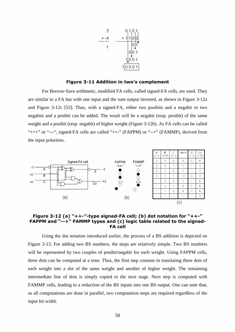
58
Figure 3-11 Addition in two’s complement
For Borrow-Save arithmetic, modified FA cells, called signed-FA cells, are used. They
are similar to a FA but with one input and the sum output inverted, as shown in Figure 3-12a
and Figure 3-12c [53]. Thus, with a signed-FA, either two posibits and a negabit or two
negabits and a posibit can be added. The result will be a negabit (resp. posibit) of the same
weight and a posibit (resp. negabit) of higher weight (Figure 3-12b). As FA cells can be called
“+++” or “---“, signed-FA cells are called “++-” (FAPPM) or “--+” (FAMMP), derived from
the input polarities.
Figure 3-12 (a) “++-”-type signed-FA cell; (b) dot notation for “++-” FAPPM and “--+” FAMMP types and (c) logic table related to the signed-
FA cell
Using the dot notation introduced earlier, the process of a BS addition is depicted on
Figure 3-13. For adding two BS numbers, the steps are relatively simple. Two BS numbers
will be represented by two couples of posibit/negabit for each weight. Using FAPPM cells,
three dots can be computed at a time. Thus, the first step consists in translating three dots of
each weight into a dot of the same weight and another of higher weight. The remaining
intermediate line of dots is simply copied to the next stage. Next step is computed with
FAMMP cells, leading to a reduction of the BS inputs into one BS output. One can note that,
as all computations are done in parallel, two computation steps are required regardless of the
input bit width.

59
Let us now consider the addition of ‘5’ and ‘-4’. Figure 3-14 illustrates three examples
of this addition, according to different possible BS representations of the numbers ‘5’ and ‘-
4’.
Figure 3-13 Addition process of two BS numbers. Little dots are free places.
Figure 3-14 Addition in BS notation
Any number representation system can be used for the addition, provided it is
represented in dot notation. For example, an easy computation is the addition of a BS number
and a C2 number in order to provide a BS number Figure 3-15. This addition uses a single
stage of FAPPM connected in parallel to provide the result. However, the MSB cannot be
computed with a simple FAMMP, because the resulting notation would not fit the BS
notation. A special-FA cell, described in Figure 3-16, has to be designed for this operation.

60
The inputs are two negabits and a posibit, and it provides a negative sum S and two carries (a
negative NC and a positive PC). The corresponding equations are also given in Figure 3-16.
Figure 3-15 Addition process of a BS number and a 2’s complement number
Figure 3-16 Special-FA cell equations, dot notation and logic diagram
In conclusion, all combinations of inputs can be computed. The addition boils down to
reduce input bits to a BS coded number, using FAMMP, FAPPM, FA and special-FA cells.
The number of steps needed for an addition strictly depends on the number of input signals to
be added. In [54], Dadda’s method is introduced to efficiently compute the sum of several
inputs. Let’s introduce the following sequence, defining the number of steps, given the
number of input signals to add (BS signals count for 2 signals, whereas C2 signals only count
for one):
2/3,...,13,9,6,4,3,2 154321 jjo uuuuuuuu ======= + Eq. 3-8
The subscript numbers denote the number of steps, while the values of the sequence
indicate the number if input signals. This confirms that for adding two BS numbers
(considered as 4 inputs), two steps are needed. However, for 3 input signals (a BS and a C2,
for example), a single step is required. Table 3-4 illustrates this method.

61
Number of input signals Number of steps
2 0 (no computation)
3 1
4 2
6 3
9 4
13 5
Table 3-4 Illustration of Dadda’s method
3.3.3 ∆Σ modulator architecture in BS
representation
This section deals with the application of BS arithmetic inside the third-order ∆Σ
modulator described in a previous part. An example of application of redundant
representation in ∆Σ modulators can be found in [55]. The ∆Σ modulator architecture is
recalled in Figure 3-17. It has been reorganized to combine adders and registers into a single
block (dynamic logic). Signals in BS notation are drawn in bold lines Bit widths for each
signal have been determined from simulations of the architecture with typical input signals.
Figure 3-17 Third-order ∆Σ modulator architecture
It is recalled that 2-n blocks are simply right shift operations, when digitally
implemented in 2’s complement notation, and do not require any computational effort.
However, with BS notation, if the signal is shifted and truncated, then there might be an error
equal to one LSB. We will see later that those errors do not cause significant performance
degradation. All stages will be detailed hereafter with the dot notation introduced earlier.

62
The first stage is presented in Figure 3-18a. It is composed of two blocks: the first one
subtracts the 13-bit input with the sign Y multiplied by 212. The second one adds a BS number
with a C2 coded number. This operation has been described in the introduction and is
depicted in Figure 3-18b. The B1 block shown on Figure 3-19 is a special case. Although it
should be possible to use a classical C2 adder for this operation, a more attractive solution is
proposed. One can observe that if Y is equal to 1, then the result of the subtraction will be
negative whereas if Y is equal to 0, the result would be positive. More generally, let us take an
input signal coded on N-bits.
When Y=0, -2g (i.e. “
0...01...1
gR−
”) must be subtracted, thus " 0...100...01−−gR
" must be added.
When Y=1, 2g (i.e. "
1...10...0
gR−
") must be subtracted, thus " 01...01...11−−gR
" must be added.
So, in both cases, " Y...Y...YgR
0101−−
" has to be added.
In the present case, 31 =−− gR , which defines the architecture for the B1 block. The
LSB addition has been deleted to avoid any carry propagation. The error introduced should
not be relevant. However, it can be corrected by inserting Y into the B2 block output signal,
because the positive LSB of the result is left empty. Finally, the B1 block of Figure 3-19 is
composed by a simple inverter.
Figure 3-18 (a) Details of the first stage and (b) dot notation associated with the B2 block

63
Figure 3-19 Details of the B1 block
The second stage is the most complicated one as it computes three BS signals and a
sum signal. This operation can be performed with three stages of signed-FA, as shown in
Figure 3-20. Y signal is considered, like in the first stage, as “ Y...Y 010 ”.
Figure 3-20 (a) Details of the second stage and (b) dot notation associated with B3,B4 and B5 computation blocks

64
Figure 3-21 (a) Details of the third stage and (b) dot notation associated with B6,B7 and B8 computation blocks
Figure 3-21 describes the third stage. The input is composed two BS numbers plus the
Y feedback signal, thus two steps are required for the addition. The last step computes the
result of B7 block with the Y input to provide the 16-bit output BS signal. Identically to
previous stages, Y is noted “ Y...YYY 010 ”. A special-FA cell is used for the MSB computation
of the last block.
3.3.4 Simulation results
Concerning the BS-implemented ∆Σ modulators, Figure 3-22 shows an evaluation of
the ACLR performances for both C2 and BS implementation. The input signal is the 8th
WCDMA channel. Performance of the BS architecture is almost identical to the C2
implementation, and even slightly better. The simulated ACLRs are 76.2 and 73.7dB,
respectively, for 5 and 10MHz offsets.
To study integrators saturation, several types of inputs have been tested. The Full-
Scale (FS) is defined as the maximum amplitude at the quantizer. For example, for a signed
16 bits input, FS is [-32768; 32768]. This modulator can accept:
• Any DC level included between -21000 and +19000, i.e. 61% of FS. This is
acceptable, because DC levels at the modulator input are rarely high and
commonly near zero.
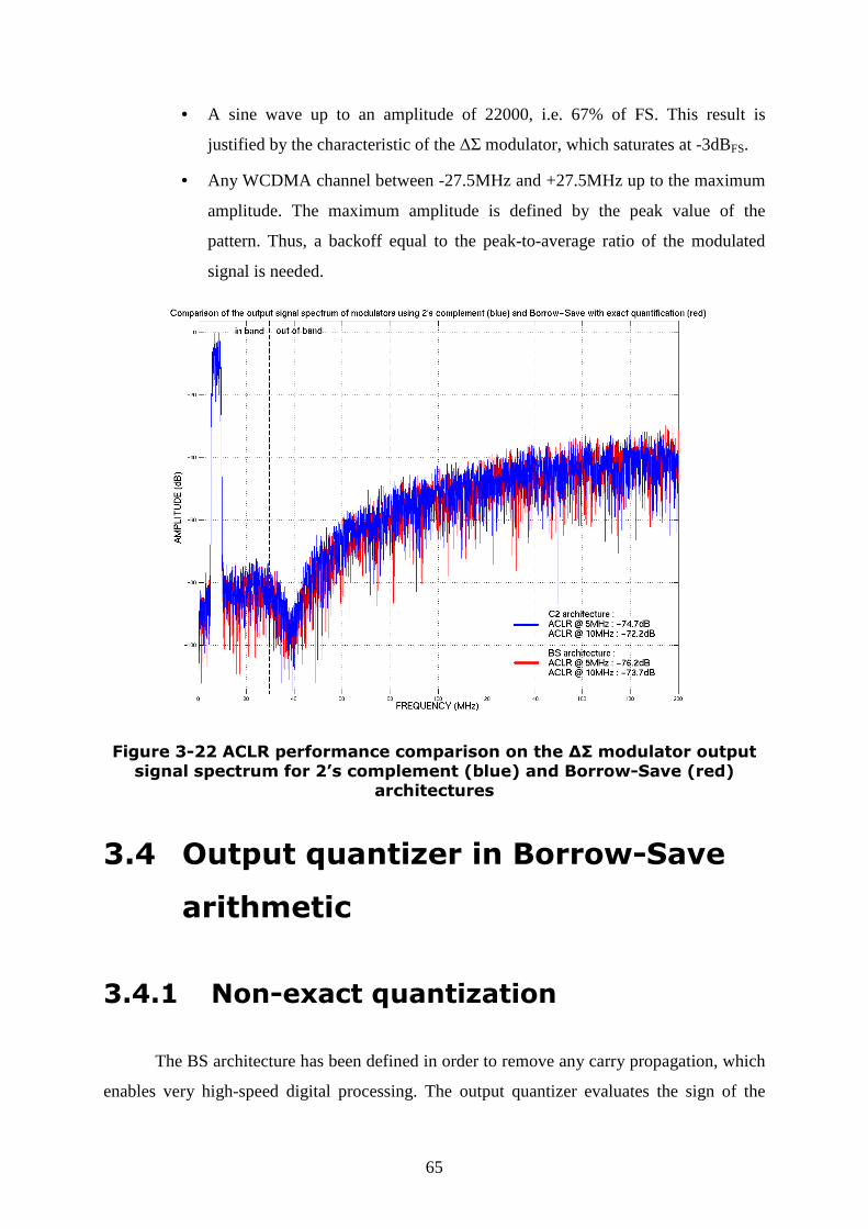
65
• A sine wave up to an amplitude of 22000, i.e. 67% of FS. This result is
justified by the characteristic of the ∆Σ modulator, which saturates at -3dBFS.
• Any WCDMA channel between -27.5MHz and +27.5MHz up to the maximum
amplitude. The maximum amplitude is defined by the peak value of the
pattern. Thus, a backoff equal to the peak-to-average ratio of the modulated
signal is needed.
Figure 3-22 ACLR performance comparison on the ∆Σ modulator output signal spectrum for 2’s complement (blue) and Borrow-Save (red)
architectures
3.4 Output quantizer in Borrow-Save
arithmetic
3.4.1 Non-exact quantization
The BS architecture has been defined in order to remove any carry propagation, which
enables very high-speed digital processing. The output quantizer evaluates the sign of the

66
output. In two’s complement representation, the sign is obviously given by the MSB polarity.
However, with BS notation, sign evaluation is not an easy task, because all bits affect the
sign. Thus, a carry must be propagated all along the 16 quantizer input bits. A logic
comparison between the positive and the negative input bits must be performed.
Unfortunately, the critical path, determined earlier, contains the output quantizer.
Therefore, any excessive propagation delay on this block must be avoided, as all the benefits
brought by the BS notation is lost in this operation.
The solution is inspired by the analog implementation of ∆Σ modulators. Dithering is
sometimes performed before quantization to avoid signal harmonics raise and to wreathe the
shaped noise [41]. Concretely, some kind of noise is added to the signal before quantization.
It is shown that this added noise does not degrade the performances as it is also shaped away
from the band of interest. Looking at this, the idea of performing a non-exact quantization
comes to the fore.
The number of bits used in the logic comparison has been progressively reduced and
∆Σ modulator performances have been evaluated. This has led to a drastic reduction in the
comparison complexity. In fact, a 3-MSB comparator is able to achieve similar performances
than a 16-bit comparator, as shown on the plot of Figure 3-23. (a) and (b) dot notations in
Figure 3-24 depict the progressive reduction of the number of bits considered in the
comparison.
To go further, a logic study of the output bits values has shown that the positive and
negative MSBs are always equal for all non-saturated input signals listed above, and that the
negative 15th bit is always null. This is depicted on the (c) dot notation. Thus, they do not
affect the output sign and can be left unused. Finally, with our architecture, the sign can be
easily computed with the equation presented on Figure 3-24.

67
Figure 3-23 Evaluation of the ∆Σ modulator performances with non-exact quantization
Figure 3-24 (a), (b) and (c): Dot notations related to the bits considered inside the logic comparator
Performance evaluation has been made in the same conditions as before, leading to the
plot of Figure 3-25. It relates a slight increase in the in-band noise for the non-exact
quantization. There is a trade-off to make between the comparator complexity and the
performances obtained. Table 3-5 sums up the ACLR values obtained with the respective
architectures. For BS implementation with non-exact quantization, the ACLR falls down by

68
about 6dB to about 68dB. For remembering, ACLR limits defined by the UMTS norm allows
-33 and -43dB for 5 and 10MHz offsets, respectively. These simulation results let a
reasonable margin for disturbances introduced by output stages.
ACLR @ 5MHz ACLR @ 10 MHz
Two’s complement -74,7 dB -72,2 dB
Borrow-Save with exact quantization -76,2 dB -73,7 dB
Borrow-Save with 3-bit non-exact quantization -68,8dB -67,4 dB
Table 3-5 ACLR comparison for different ∆Σ modulator architecture
Figure 3-25 ACLR performance comparison on the ∆Σ modulator output signal spectrum for BS architecture with exact (red) and non-exact (red)
quantization

69
3.4.2 Output signal precomputation
Figure 3-26 Precomputation of the sign; Y is evaluated in parallel with the stage 3 output signal.
Although the output comparator complexity is greatly reduced, its computation needs
available time to be correctly performed, which is not the case in the implementation
explained in the previous parts. Parallelizing the comparator operation with the computation
inside the third stage seems to be a good solution to physically implement the global function.
This is what is called precomputation of the sign. It is depicted on Figure 3-26, with the sign
evaluation in parallel with the B8 block.
Let’s take the general case of Figure 3-21b in which two BS signals are added together
with the C2-coded Y signal. If the comparison is made on the two MSBs, then the global logic
operation to perform is )( 161615151616−+−+−+ ++= OutOutOutOutOutOutY to evaluate the sign of
the signal. There are two possibilities to determine the sign of the BS signal, because zero can
be assimilated either to a positive or to a negative number. Thus, either
)( 1616151616−+−−+ ++= OutOutOutOutOutY or )( 1616151616
−++−+ ++= OutOutOutOutOutY can be
chosen. The first equation is more practical, as it uses 15−Out , which is directly produces by a
special-FA at the same time as 16+Out and 16
−Out , from the A15, B15 and Y bits, as denoted on
Figure 3-21b. Combining this logic equation with the special-FA ones, one can demonstrate

70
that YBYABAY 15151515 ++= . This is the precomputed equation for 2-bit sign evaluation and
can be easily computed as only three terms are used.
The same reasoning can be executed if a 3-bits comparison is pointed out. The initial
logic equation is )()( 16161514151616−+−−+−+ +++= OutOutOutOutOutOutOutY and can be reduced to
))(( 151514141515 YBYABABAY +++= , while considering the B8 block equations. Five terms
are used here which leads to a more complicated precomputation.
Moreover, the comparator block could be placed in parallel with the B7 and B8
blocks, but, in most cases, the number of different terms to compute grows with the depth of
precomputation. Thus, this solution has been aborted.
Finally, the global idea is to find the easiest equation (involving minimum terms) for
precomputation, even sometimes by reorganizing addition structures inside the third stage.
3.5 Conclusion
The system design of the third-order ∆Σ modulators has been covered by this chapter.
First, the global architecture has been defined. Then, a logic description has stated the
limitations in terms of high-speed implementation with a 3.9GS/s sample rate. Techniques for
achieving this high sample rate have been developed.
• The use of redundant arithmetic inside the modulator enables carry-free
additions. So the maximum length critical path is reduced to three full-adders.
• A dynamic logic transistor implementation will help in performing the
additions. This aspect is process dependent, hence, for future CMOS
technologies, dynamic logic can be replaced by easy-to-implement static logic
using, for example, pass-transistor logic. The dynamic logic used in our
architecture will be described in next chapter, which deals with transistor
design.
• A non-exact quantizer is designed to reduce the borrow-save sign evaluation
complexity, which needs carry propagation.

71
• An output sign precomputation parallelizes the non-exact quantization
operation with the last computation stage, in order for the output signal to be
available for the next sample period.
All these techniques (except dynamic logic) for achieving high-speed ∆Σ modulators
are deeply covered by a co-authored patent [56] and a conference paper [57].


73
CHAPTER 4
DIGITAL TRANSMITTER CIRCUIT
DESIGN
4.1 Transmitter IC description
4.1.1 IC structure
Figure 4-1 Processing blocks implemented inside the transmitter IC prototype
The designed transmitter IC comprises all processing blocks highlighted on Figure
4-1. The core is the delta-sigma modulators, associated with the digital quadrature
upconverter. It also handles clock generation and distribution, pre-amplification and a part of
the sample rate conversion block (the 16-time oversampling sub-block). For demonstration
and control purposes, a few blocks are added, as shown on Figure 4-2. These ones are the
Delay Locked Loop (DLL) block, the output registers and the control block. The DLL block
provides finely controlled delayed clocks from a unique external master clock. Output
registers are useful for testing purpose. They act as serial-to-parallel (S/P) converters. The
control block provides all the useful signals for proper operating conditions.

74
Figure 4-2 IC block structure
For describing the whole transmitter circuit design, the outline will be as follow. The
global structure and layout will be presented. Then, inside the following sections, we will
detail the circuit design and the generated layout for each block separately: the sample rate
converters, the delta-sigma modulators, the DLL block and the digital quadrature upconverter.
Output registers will not be detailed as they are commonly implemented. The control block
will not be investigated either, as signals of interest will be evoked inside main processing
blocks description.
4.1.2 IC configuration and layout
The first prototype transmitter IC has been designed in STMicroelectronics 90nm
CMOS process. The layout is shown on Figure 4-3. It sizes around 13× mm² and counts 96
pads. Top (resp. bottom) side comprises the 13-bit I (resp. Q) input and half of the
parallelized I (resp. Q) outputs. I and Q signals at the 3.9GS/s output of the ∆Σ modulators are
parralelized into 243.75MS/s 16-bit streams. The choice has been made, for reducing the pin
count, to output only the first 8-bit half or the second 8-bit half of this stream and a control
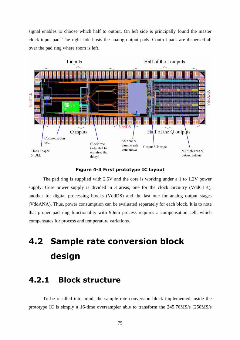
75
signal enables to choose which half to output. On left side is principally found the master
clock input pad. The right side hosts the analog output pads. Control pads are dispersed all
over the pad ring where room is left.
Figure 4-3 First prototype IC layout
The pad ring is supplied with 2.5V and the core is working under a 1 to 1.2V power
supply. Core power supply is divided in 3 areas; one for the clock circuitry (VddCLK),
another for digital processing blocks (VddDS) and the last one for analog output stages
(VddANA). Thus, power consumption can be evaluated separately for each block. It is to note
that proper pad ring functionality with 90nm process requires a compensation cell, which
compensates for process and temperature variations.
4.2 Sample rate conversion block
design
4.2.1 Block structure
To be recalled into mind, the sample rate conversion block implemented inside the
prototype IC is simply a 16-time oversampler able to transform the 245.76MS/s (250MS/s

76
will be used in the sequel for more conciseness) input sample rate into the 3.9GS/s rate of the
delta-sigma modulators. This operation is not difficult to implement as it is only composed by
registers, as shown on Figure 4-4. In the clock scheme used, the IC provides the 250MHz
main clock and the output stages of outside components (mainly FPGAs) are sampled with
this clock. It avoids outside generation of synchronous clocks. However, other schemes could
be used, which are synchronicity-independent. For example, for the second prototype IC, the
clocking scheme has been modified. Clock is provided by the outside and resynchronized on
the input. It is depicted on Figure 4-5. This data acquisition process will work whatever is the
phase relationship between the clocks. We will see in the next chapter on test equipment that
the second solution is more practical to implement.
Figure 4-4 Input sample rate conversion block and clock scheme

77
Figure 4-5 Clock scheme used for data acquisition in the second prototype IC
As described in a previous chapter, an operation of linear interpolation must be
accomplished on Q channel to avoid images from rising above the quantization noise. Since
the input signals are oversampled 16 times with a sample-and-hold function, the resulting
operation, described in Figure 4-6, is relatively simple. The input symbol on Q channel is
repeated 15 times, while the 16th one is calculated from two successive symbols. This can be
implemented using the structure of Figure 4-7. The switch command is used to place the
calculated 16th symbol at the right place. This switch command is easily generated from the
250MHz clock. Registers sampled at 4GS/s delays it and an appropriated logic gate combines
the original clock with the delayed one and thus produces the switch command. It is to note
that an equivalent delay is introduce on I channel for synchronicity.

78
Figure 4-6 Qualitative I and Q signals at the ∆Σ modulators input. Q signal has been linearly interpolated on each sample.
Figure 4-7 Linear interpolation on Q channel inside SRC block
4.2.2 TSPCFF registers
For transistor implementation, D flip-flops able to work at few GHz must be designed.
The edge symmetry is also a criterion of choice. In literature, the dynamic True Single Phase
Clock Flip-Flop (TSPCFF) appears to be one of the fastest [28]. Moreover, as stated in its
name, it uses a single phase clock, which is a valuable asset. The schematic and layout of this
flip-flop is displayed on Figure 4-8. The layout sizes 5.44.5 × µm².

79
Figure 4-8 Schematic and layout of the TSPCFF
Figure 4-9 describes the mechanism of operation. When the clock signal is low, D2
node is stuck at Vcc through the conducting PMOS. This phase is called “precharge”. Thus,
out1 node is left high impedance and out node is its complementary. These latter nodes keep
their preceding values (“hold” phase). D1 node is the complementary of D input.
When the clock signal goes high, then D2 becomes dependent over the D1 value. This
is called “evaluation”. If D1 is low, then D2 does not change its precharge value. If D1 is
high, then D2 node is discharging through the NMOS transistors. The nodes out1 and out
follow the D2 node as they are in an inverter configuration (“active” mode).
The registering operation is very fast, but output edges rise and fall times and related
propagation delays could be very different. First, output NMOS and PMOS are sized in order
to equalize rise and fall times. Let’s detail the reasons why propagation delays could be
different to find an acceptable solution.
In the case of a rising output edge, the hold value of out1 is 1. When made active with
the rising edge of the clock and D2 evaluated as 1 (not discharge), then the time for out to
become 1 is the time to discharge out1 and charge the out node.
In the case of a falling output edge, the hold value of out1 is 0. When made active with
the rising edge of the clock, D2 is evaluated as 0. This node must discharge before out1 and
out gets their values. Thus, the time for out to become 0 is now equal to the time taking to
discharge D2, charge out1 and then discharge of out node.
An acceptable solution for equalizing the propagation delays for each transition is
equating the out1 discharge time with the D2 discharge plus out1 charge times, by adjusting
sizes of N and P MOS transistors. In fact, out1 discharge must be slowed down whereas its

80
charge must be fastened. This can be made by simulating the flip-flop to find the best
optimization. An eye-diagram for an 8GHz clock, presented on Figure 4-10, describes the
performance of the optimized flip-flop. The output rise and fall times are varying from 17 to
22ps depending of the process corners (fast or slow). The propagation delay is equal to 40ps
for the best implementation case.
Figure 4-9 Mechanism inside the TSPCFF when clock signal is low (left) and high (right)
Figure 4-10 Eye diagram of the TSPCFF output signal for a typical process corner and a temperature of 80°C

81
4.3 Digital delta-sigma modulator
circuit design
4.3.1 Global structure
Figure 4-11 Third-order ∆Σ modulator architecture
The third-order ∆Σ modulator architecture is drawn on Figure 4-11. As described on
Figure 3-18, Figure 3-20 and Figure 3-21, each stage comprises, at the most, three logic
layers, each built up from signed-FAs, signed-HAs or buffers. From this statement, the idea is
to design a brick-like architecture. As the gate switching speed is the main parameter for our
application, the previous chapter has stated dynamic logic was the logic style of choice. Using
differential dynamic logic does not require any register anymore because the storage function
is implicitly implemented. However, each dynamic logic layer requires its own clock to be
functional. Thus, for three logic layers, three clocks would be used, each delayed from the
others by a third of the period. Figure 4-12 depicts the layout of the dynamic logic base
bricks. A DLL (explained later) will be useful to generate multiphase clocks.
Each differential dynamic logic layer will be evaluating the gate output into a third of
a period. During the unused time, the dynamic gates will precharge themselves to be ready
when their respective clocks will rise up.

82
Figure 4-12 Layout of the basic bricks and relationship between the three different clocks
4.3.2 Dynamic FA circuit description
Figure 4-13 Differential dynamic FA cell circuit diagram (transistor gate lengths are minimal)
Details of a differential dynamic Full-Adder cell are presented on Figure 4-13. The
principle of operation of such a cell is quite similar to the dynamic flip-flop cell presented

83
earlier. It counts two succeeding stages: a precharge/evaluation stage followed by a
hold/active clocked inverter (tri-state inverter). When the clock is low, intermediate nodes are
precharging to the high state through the PMOS transistors and the outputs are high
impedance. At the moment the clock signal is turning to ‘1’, outputs are made active and
reflect the intermediate node evaluation. One intermediate node over the two stays high,
whereas the other one is discharging itself into the conducting FA NMOS logic and the
clocked NMOS. FA logic for sum and carry evaluation is not depicted here as it is simply a
differential NMOS logic network.
Figure 4-14 Transient response of a FA cell with an ideal clock
A transient simulation of such a cell can be found on Figure 4-14. For this simulation,
inputs of the FA cell are chosen to be a 3-bit counter; hence there are 8 states in the graph.
The simulation is done with a 250ps ideal clock with 30ps rising and falling edges. We can
observe, from top to bottom, the clock, the intermediate precharge node, the sum output, the
differential intermediate precharge node and finally the differential sum output. Evaluation
and precharge phases have been displayed prominently. During precharge, all intermediate
nodes are precharged to 1 (up arrows), while the outputs are held (right arrows). During
evaluation, the intermediate nodes are evaluated to the computed value. The output sums are
inverted and then take their final value for the period.

84
The propagation delay of this gate is around 50ps in the worst case when loaded by an
identical gate. Larger output loads and additional initialization circuitry, which will be
discussed hereafter, will slightly increase this value. One can note that in any case the
effective propagation delay is not defined by the circuit itself, but rather by the third of the
applied clock period, assuming the circuit could operate at the desired rate.
For validation, the global transistor circuit has been simulated and bit-to-bit compared
to system simulations. It does not show any discrepancies.
The global consumption of the whole ∆Σ modulator with its initialization circuit has
been evaluated by simulations, as though it is not the critical point of this study, contrary to
speed enhancement. It would consume around 20mW. A previous identical design with a
130nm process has shown a consumption of 36mW. We can hopefully think that a further
technology shrink (65nm process) will still reduce this estimated consumption.
4.3.3 Initialization circuitry
A major drawback is that this system comprises feedbacks. In fact, if no care is taken,
the two nodes of a differential signal could be equal when powering up the system. Then, as
outputs are fed back on inputs, the non-differentiality of these signals keeps the circuit stable
into this bad and non-operating state. So an initialization phase is fundamental.
Forcing outputs to be differential is a solution to ensure a good startup of the system.
Thus, a reset signal is needed, coming from outside the chip or from the locked flag of the
DLL. To implement this control, two transistors are added inside the block controlled by
CLK3, as shown on Figure 4-15.
On this figure, clocked inverter symbols have replaced the previous transistor diagram
for the sake of clarity. The added transistors are controlled by the complementary signal -R,
active when high. It forces the SUM output to be low by pulling its level through a NMOS
transistor. No conflict happens because SUM is either high impedance or logically stuck at ‘0’
when in the reset state.
For the complementary output _SUM, the intermediate node is pulling down only
when the clock signal is high, in order to avoid conflict when this node is precharging. For
that purpose, the NMOS transistor width has been reduced. If not, a non-defined level
between high and low state might appear during precharge.

85
Figure 4-15 Dynamic FA cell circuit diagram, including the reset circuitry
A potential problem now appears when the reset signal is relaxed (from ‘1’ to ‘0’).
Examine the case when the reset signal is released during of the evaluation period (clock is
high) and that the expected evaluation result is 1=SUM and 0_ =SUM . The intermediate
node for SUM will be discharged during the evaluation period and when the reset is relaxed,
SUM output will stick at ‘1’ (provided the reset signal left time for the level to rise). For the
complementary intermediate node, the FA logic will not be conducting but the reset-
controlled transistor will be, so this node will also discharge itself and could never rise again
before the next period. That means _SUM output will stick at ‘1’. SUM and _SUM would not
constitute a differential signal anymore. Errors will propagate to all nodes due to the ∆Σ
feedback structure. To sum up, the reset signal must relax itself during a precharge period.
To perform this, the reset signal has to be synchronized with the clock signal, what is
not easy to realize and would not operate for a wide range of frequencies.
In a perspective of configuration, another initialization circuitry has been developed. It
is illustrated on Figure 4-16. The cross-coupled NMOS transistors have two purposes. The
first one is to maintain a differential output signal whatever are the inputs. Only one side can
discharge, as it automatically blocks the other side. Secondly, this structure acts as a latch, so
it can operate at any frequency (of course limited by the worst case propagation delay).

86
Unfortunately, the addition of this cross-coupled transistor slightly slows down the operation,
compared with the above architecture.
Figure 4-16 Dynamic FA cell circuit diagram, with an improved reset circuitry (The FA logic has been split in two differential blocks)
4.3.4 ∆Σ modulator layout view
The layout of the ∆Σ modulators is rather dense, because of interconnections between
the base blocks. A strategy for correctly connecting all these blocks must be adopted.
STMicroelectronics CMOS 90nm technology offers 7 levels of routing metal (two uppers are
thick metal levels). Figure 4-17 details the routing strategy and the different types of
interconnections. The three sum stages are staggered and shifted according to the
multiplicating power-of-two factors. Thus, direct connections from one block to the following
are routed straight ahead in second and third metal levels (first level is kept for internal cell
routing). The integrators feedbacks are integrated into each stage. Stage outputs are routing
directly back into stage inputs on the third metal level. Then, the global feedback is routing
over the second and third stages, using fourth metal level. Finally, the output sign is fed back
to the requested inputs using fifth and sixth metal levels.
Clocks and reset signals are routed vertically in an upper metal with a ladder type
routing and access points to the cell are spread all over the distance. Power supplies and

87
grounds are not represented on this figure. They are horizontally comb-routed all over the ∆Σ
modulator layout.
Figure 4-17 ∆Σ modulator layout routing strategy
One can observe on the left of Figure 4-18 the arrangement of the three stages and the
network of interconnections. Power supplies and ground rails are not shown. A bit slice has
been highlighted and zoomed in on the right of the figure. On it, one can observe the clock
and reset distribution rails as well as the three logic cell inside each sum stage.
Details of the dynamic signed-FA cell layout are given underneath. Two parts
compose this cell: a fixed part implementing the dynamic logic circuitry for precharge and
evaluation and a configurable part, which lets one choose the desired logic function to realize
(sum or carry in the case of a FA).

88
Figure 4-18 ∆Σ modulator layout
4.4 Clock generation and distribution
To make dynamic cells operating, three clocks, at 0°, 120° and 240° are needed [58].
They are produced with a Delay Locked Loop (DLL). Its principle of operation is illustrated
on Figure 4-19 [59]. The main component is a controlled delay line in which delays are
functions of an applied voltage. In this case, three identical delay elements deliver the desired
clock signals. To be able to synchronize these clocks on a reference clock, the phase of the
latter one is constantly compared with the phase of the last generated clock (CLK3). The
phase detector will provide the phase information to a charge pump. From this information,
the voltage applied to the delay line will be increased or decreased. Thus, CLK3 will be
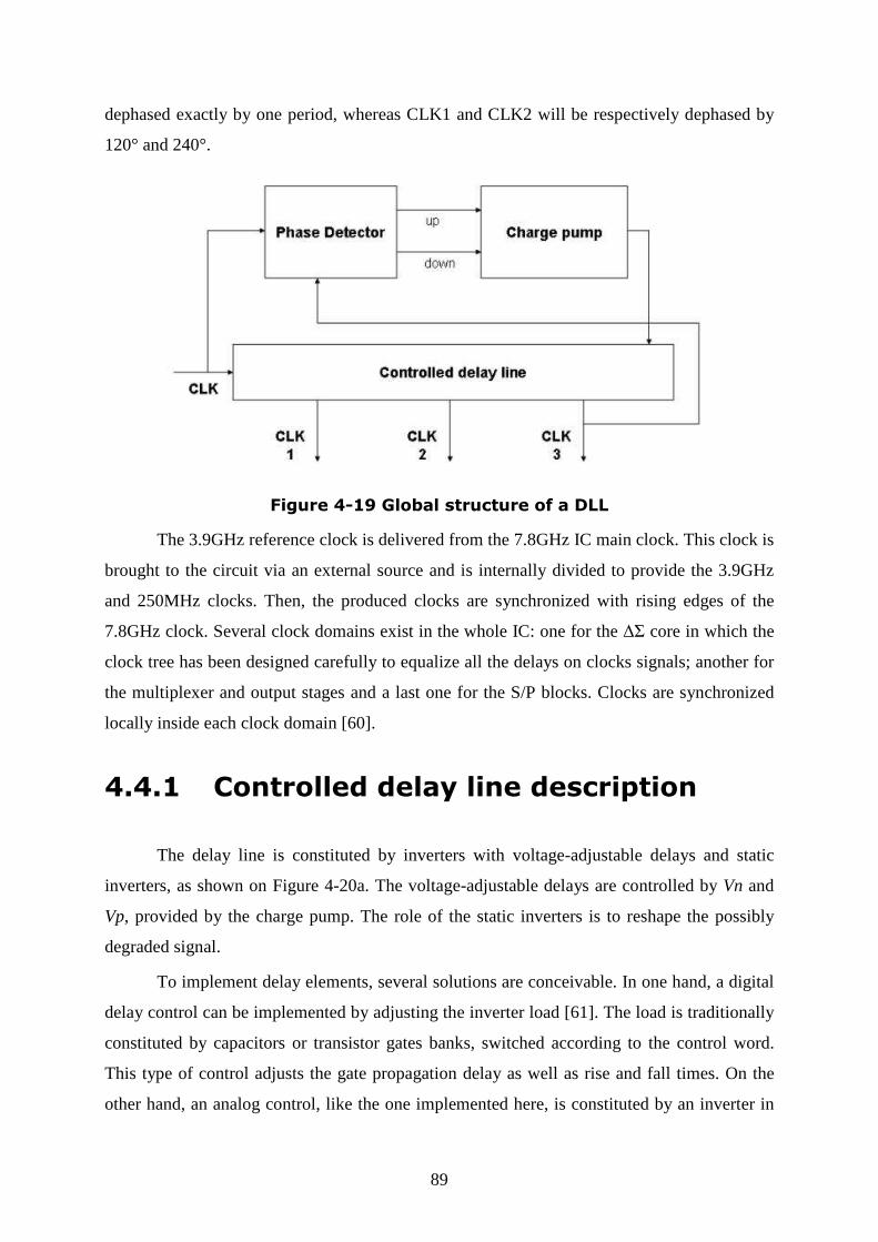
89
dephased exactly by one period, whereas CLK1 and CLK2 will be respectively dephased by
120° and 240°.
Figure 4-19 Global structure of a DLL
The 3.9GHz reference clock is delivered from the 7.8GHz IC main clock. This clock is
brought to the circuit via an external source and is internally divided to provide the 3.9GHz
and 250MHz clocks. Then, the produced clocks are synchronized with rising edges of the
7.8GHz clock. Several clock domains exist in the whole IC: one for the ∆Σ core in which the
clock tree has been designed carefully to equalize all the delays on clocks signals; another for
the multiplexer and output stages and a last one for the S/P blocks. Clocks are synchronized
locally inside each clock domain [60].
4.4.1 Controlled delay line description
The delay line is constituted by inverters with voltage-adjustable delays and static
inverters, as shown on Figure 4-20a. The voltage-adjustable delays are controlled by Vn and
Vp, provided by the charge pump. The role of the static inverters is to reshape the possibly
degraded signal.
To implement delay elements, several solutions are conceivable. In one hand, a digital
delay control can be implemented by adjusting the inverter load [61]. The load is traditionally
constituted by capacitors or transistor gates banks, switched according to the control word.
This type of control adjusts the gate propagation delay as well as rise and fall times. On the
other hand, an analog control, like the one implemented here, is constituted by an inverter in

90
which a NMOS and a PMOS has been added in series in the main branch, as on Figure 4-20b
[62]. The rise and fall times are better controlled than with the digital control. Only one
NMOS or PMOS could be used, but it would unbalance the rise and fall times of the clock
signals.
Figure 4-20 Inverter chain constituting the voltage-controlled delay line
4.4.2 Phase comparator and charge pump
The phase comparator provides information about the phase relationship between the
reference clock and CLK3. Its principle of operation is described on Figure 4-21. In a first
step, clock frequencies are divided by two in order for the succeeding computations not to be
critical. The phase detector is waiting for a rising edge on each clock to reset its output
(Figure 4-22). The RS flip-flop triggers on with the first rising edge and keeps holding its
value until the second sets in. Its output signal is returning to zero when inputs are falling
down. This flip-flop provides an UP signal, meaning the voltage Vn must be increased and a
DOWN signal, meaning it must be decreased. The charge pump brings or removes a defined
charge quantity from the storage capacitor. Vn is then obtained on the capacitor and Vp is
created using a diode-mounted transistor in order to have VnVddVp −= (give or take the
transistors threshold voltages). Adequate controlling voltages are obtained from this phase
comparison.

91
Figure 4-21 Phase comparator and charge pump schematics
Figure 4-22 Phase comparator and charge pump signals
4.4.3 DLL mechanism and clock signals
characteristics
The DLL has two operating phases: a calibration phase and a locking phase. In the
initial state, delays are set to the minimum by sticking Vn to Vdd. During calibration, Vn

92
voltage is decreasing slowly and Vp increases similarly, until they stabilize when the clocks
are locked in phase (Figure 4-23). Then, the charge pump is continuously adjusting the
voltage around this locking state. In simulations with a 100µA current source for the charge
pump, the calibration phase lasts between 50 and 100ns for a few GHz clock.
Figure 4-23 Evolution of Vn and Vp during calibration and locking phases
Figure 4-24 CLK1, CLK2, CLK3 and reference clock waveforms.
Figure 4-24 shows output signals of the DLL for a 4GHz clock (250ps period) when
locked. The locking error between CLK3 and the reference clock is around 5 picoseconds.
Simulated clock characteristics are summed up in Table 4-1. Duty cycles are near 50% and
rise and fall times are acceptable.

93
Duty cycle Rise time Fall time Phase delay (+/ 5ps)
CLK1 51% 37ps 23ps 83ps (33%)
CLK2 51% 38ps 23ps 84ps (34%)
CLK3 52% 43ps 25ps 84ps (34%)
Table 4-1 DLL clocks characteristics for 4GHz clock reference. The load is constituted by one ∆Σ modulator.
Consumption has been evaluated during simulations. It largely depends over the sizes
of the chain delay transistors. For about 100µm width PMOS and 50µm width NMOS, the
calculated consumption is around 50mA under 1.2V. We could expect this consumption to be
greatly reduced going though next generation technology process. It is to note that for further
configurable architectures, wide-range DLLs must be designed [63].
4.5 Digital mixer and output stages
design
A previous section has described the digital mixer and output stages principle of
operation and different types of non-idealities brought to the output signal of this stage. It has
been stated that edges symmetry must be guaranteed by the use of a differential structure, as
shown on Figure 4-25. In fact, all symbols must have the same energy. The digital mixer
stage will be designed with great care for generating a signal with the most symmetric edges.
Figure 4-25 Differential output stages architecture
It must be considered that processing the signal into these stages correspond to a
conversion from digital to analog [64]. Thus, the above structure must operate independently
of the data and of the operating sample rate, in order to equalize the energy for each bit and to
respect RF signal integrity.

94
4.5.1 Digital mixer structure
The study of the digital mixer structure is part of Axel Flament’s thesis work and is
fully detailed in his thesis report [65] and in an article [64]. Here are only given some
elements for understanding.
The digital mixer relies on a multiplexing operation. It could be realized with D flip-
flops and transmission gates, as illustrated on Figure 4-26. The first transmission gates let us
choose either I (resp. Q) or its complementary (resp. Q complementary). The second gates
selects either I channel or Q channel. Three clocks and their complements have to be used
with this architecture: one at 4 times the carrier frequency fc (7.8GHz), another divided by two
(3.9GHz) and the last one at fc (1.95GHz). They are produced and synchronized locally, as
they are only used there.
Figure 4-26 Multiplexer architecture
Critical paths for this architecture are presented in the left of Figure 4-27. The
architecture must ensure that data going through the last flip-flop have traveled the same path
length and established themselves with the same accuracy. This is to keep the delay data-
independent, which is not obvious to realize with high-frequency switching.
Highlighted critical paths have different lengths due to the opposite phase clocks
controlling the transmission gates. To synchronize critical paths, a TSPCFF is inserted on Q
channel and clocks phase controlling transmission gates are inverted. The computed function
stays identical, but now time to reach the input of the last flip-flop is rigorously identical for I
and Q channel. Delays has become independent over data and working frequency.

95
Figure 4-27 Multiplexer architecture, showing (left) critical paths and (right) the adopted solution for data-independent signal paths
4.5.2 Output stages
Output stages following the digital mixer are acting both as a pre-amplifier and as a 1-
bit digital-to-analog converter. They are simply a chain of growing inverters, able to drive a
50Ω load under a 1V power supply. Inverters had to be sized in order to guarantee the output
signal edge symmetry. A simulated eye-diagram is shown on the left of Figure 4-28 to outline
obtained performances at the differential output of the buffers for an 80°C temperature and a
slow process corner. We show a zero-crossing differential signal with 23ps rise and fall times.
Modeling pads and bonding wires to come closer to a realistic simulation leads to the eye-
diagram on the right of Figure 4-28. It depicts rising and falling times twice than simulations
without pads and bonding wires models.
Figure 4-28 Eye diagrams for 50Ω-loaded buffers differential output signals for a slow process corner at 80°C (a) without and (b) with an
electrical model for pads and bonding wires

96
4.6 Conclusion
A first 96-pad 13× mm² prototype IC has been developed in STMicroelectronics
CMOS 90nm technology. Circuit diagrams and layout for the main parts of the prototype IC
have been explained in full details into this chapter:
• The sample rate conversion blocks, including the interpolation circuit on Q
channel, has been detailed. A focus has been made on the design of high-speed
dynamic flip-flops, known as True Single Phase Clock Flip-Flops (TSPCFF)
• The digital ∆Σ modulators have been fully covered, with a top-bottom
approach and emphasizing on initialization circuits and layout arrangement.
• The Delay-Locked-Loop multiphase clock generation block has helped in
dealing with dynamic logic inside the ∆Σ core by providing three dephased
clock signals.
• Finally, the digital mixer, digitally implemented by a multiplexing operation
and output buffering stages has been reviewed.
Inside those circuit descriptions, other architectures have been propounded. They will
be used in a second prototype, detailed in next chapter. This second prototype will enhance
the first version and correct some unsuccessful choices.
Implementation of dynamic gates requires a clock generation block, initialization
circuits and a complex layout. But, at the moment, if this circuit wants to be demonstrated,
then the switching speed is the priority. In a near future, design complexity would be reduced
by using high-speed static logic gates, like DPL logic style. Consumption would also be
greatly reduced, by removing DLL blocks, which consume a lot.

97
CHAPTER 5
EXPERIMENTAL RESULTS
5.1 First prototype IC (FULBERT I)
5.1.1 Test hardware description
5.1.1.1 Measurement tools
The first prototype IC has been described in the previous chapter and its structure and
layout was presented on Figure 4-2 and Figure 4-3, respectively.
The scheduled measurements are the analysis of the analog output spectrum and the
recovery of the output digital data stream. These two test protocols are depicted on Figure 5-1
and Figure 5-2, respectively. A sine wave generator provides the 7.8GHz main clock to the
device under test (DUT). This clock is centered on 0.5V with a DC bias tee. The differential
outputs are directly connected to a spectrum analyzer through DC blocks.
Data from I and Q channels are sampled at 250MS/s. As we do not possess or have
access to an arbitrary waveform or pattern generator, which can handle this sample rate, a less
powerful arbitrary waveform generator (AWG420 [66]) is used to produce a digital 16-bit
wide word at 125MS/s. FPGAs are implemented and programmed to upsample the incoming
signal and filter out images. The signal is brought to the DUT through an impedance-
controlled connector (MICTOR). Another FPGA is used to make an interface to the logic
analyzer, decreasing the sample rate of the output digital stream. It is to note that the test must
be done twice, because only half of the output stream is output during each run. A marker is
generated at the beginning of each test run to be able to recall the good sequence. For clock
management, the clock scheme is the following: the DUT provides a 250MHz clock to the
FPGAs. The latter ones generate a synchronous 125MHz clock and control the measurement
instruments. The two 125MHz clocks could have a different polarity, depending on which

98
edge of the 250MHz clocks is counted up first into the FPGAs, leading to synchronization
issues. Another clock scheme strategy will be adopted in the second prototype.
Figure 5-1 Test hardware for the analog output analysis
Figure 5-2 Test hardware for the digital output test
5.1.1.2 Test boards and assembly
Several printed boards are designed to realize this test. First, as ICs are delivered
naked, a substrate must be designed. ICs will then be wire bonded onto the substrate. The

99
substrate will then be soldered onto a daughter board, on which are placed all the circuits for
control, analog I/Os and power supplies. Finally, the daughter board is placed on a
motherboard through high-speed impedance-controlled MICTOR connectors. The
motherboard hosts the FPGAs, programming interface, memories and all the connectors for
connecting instruments.
The substrate is a FR4, 4-layer, 1224× mm² printed circuit board (PCB) with state-of-
the-art constraints on track width and isolation. Tracks on which the IC will be bonded are
50µm wide and spaced by 50µm from other tracks. As the IC pad pitch is 80µm and the PCB
pitch is 100µm, angles at extremities are around 40°, which is in fact too high for a reliable
and repeatable wire bonding operation. Figure 5-3 shows a picture of the substrate on which
an IC has been wire bonded at the center. Figure 5-4 shows the daughter board and the
motherboard.
Figure 5-3 IC wire bonded on the substrate, soldered on the daughter board

100
Figure 5-4 Daughter board (left) and motherboard (right)
5.1.2 Measurement results
5.1.2.1 Issues
When measurements were executed, a main issue had appeared. Huge oscillations on
power and ground inside the chip have been observed, when the sample rate was increased. In
fact, not enough decoupling capacitance was present on-chip, as the only decoupling was
lying inside some pad ring cells. Moreover, the core power supply is divided in three parts:
clock, ∆Σ core and output stages. There were not so many power supply pads for each
separated supply. As the circuit is wirebonded and huge current peaks (especially on clocks
and output stages) flow into the wires, voltage potential differences are created according to
the well know inductance equation:
dt
dILU = Eq. 5-1
This effect has been post-simulated to confirm the problem. Bonding wire inductance,
ground-related capacitance and resistance have been evaluated according to its shape and
fitted with an electrical model. This model shows that bonding wires introduce around 1nH of
inductance.
With this values and assuming an ideal off-chip power supply, transient simulations
have been performed. The simulation concentrates on on-chip supplies and clock signals as
shown on Figure 5-5. The clock goes through the vddCLK domain, then through vddDS
domain. Unfortunately, the vddCLK supply shows large variations (around 500mVpk) when
the chip is enabled, due to high current peaks in this clock domain. vddDS only slightly varies

101
(<100mV). Figure 5-6 shows effects of supply variations on signals. Clock signals hardly
suffer from the vddCLK variations, especially during the phases when the voltage is
decreased. It behaves as the gates operation is frozen by the low voltage supply. Thus, when
the clk7g8 signal is going through the vddDS domain (not affected by that disturbance) then
the resulting clock does not look like a clock anymore. The high-speed functionality of the IC
is deeply affected by this effect and could not be demonstrated.
Figure 5-5 IC post-simulation with bonding wires
Figure 5-6 Transient post-simulation according to Figure 5-5

102
For lower operating frequencies, the circuit does not suffer from those huge variations.
Unfortunately, the ∆Σ core could not be initialized properly, because the reset circuit
presented on Figure 4-15 is not working for a wide range of frequencies. It has been designed
for working with a 7.8GHz main clock. At low frequencies, the ∆Σ outputs are not differential
as they would be.
So, supplies variations prevent the high-speed operation, while low frequency
operation is not authorized by the initialization stages. A second prototype, detailed in next
subpart, has been designed to correct these two points.
5.1.2.2 Output stages measurements
The only achievable measurement on this circuit is an evaluation of the output stages,
when the circuit is on reset state. The ∆Σ outputs are then stable and differential. Thus, the
output sequence is [ ] [ ]1,1,0,0,,, =QIQI . In that case, the output is a periodic signal with a
frequency equal to the main clock frequency divided by 4. An eye diagram has been drawn on
Figure 5-7, although the signal is not randomly distributed, in order to figure out the output
signal shape for a 3.9GHz input clock (half the desired operating frequency).
Figure 5-7 Eye diagram of the IC output for a 3.9GHz input clock. The IC has been placed in its reset state
A measurement concerning output stage consumption has also been realized. The
output stage consumption (comprising digital mixer and output buffers) has been noted down
for different frequencies. The circuit has been put in its reset state and the supply voltage was
0.95V. The obtained result is presented on Figure 5-8. The useful current flowing through the

103
50Ω load is approximately equal to 18mA. The output stages current consumption increases
with the frequency with a slope of about 8mA/GHz. Thus, we can extrapolate to the desired
frequency of 7.8GHz. Switching losses will reach about 60mA, which results in a maximum
efficiency of 25% (the efficiency is here defined as the load current to the total current ratio).
Figure 5-8 Current consumption in output stages
5.2 Second prototype IC (FULBERT II)
5.2.1 Changes and enhancements
Figure 5-9 Layout of the second prototype IC

104
Figure 5-10 Die microphotograph of the prototype chip in 90nm CMOS
Test of the first prototype IC has revealed crucial points to be redesigned in order for
the circuit to be functional. Changes and enhancements have been brought to a second
prototype IC in STMicroelectronics 90nm CMOS. As the circuit is a redesign, its structure is
similar to the first prototype. Layout of this circuit is presented on Figure 5-9 and die
microphotograph on Figure 5-10. Here are the main changes from the first attempt:
• The circuit is now sizing 8.04× mm² and counts 103 pads.
• Assembly has been restrictive for the first prototype, because chosen
dimensions were at the PCB technology limits. The signal pad pitch has been
enlarged to 150µm, according to the easier and cheaper PCB fabrication.
Moreover, ground pads have been intercalated between each signal pads. For
the assembly, a large ground plane is placed under the IC and all grounds are
wirebonded on it. Signals are wirebonded a little further to 75µm-wide tracks.
With that kind of assembly the ground would be almost perfect inside the chip.
• All power supplies inside the circuit have been connected together. This unique
power supply will be equal to 1 or 1.2V. We lost the possibility to evaluate the
power consumption of each block separately but, as power pads are
disseminated all over the map, the bonding wires global inductance will be
decreased. It should be better for making a reliable power supply.
• Digital outputs have been suppressed to gain room.
• On-chip decoupling capacitors have been added to avoid variations over supply
voltages. The total added capacitance is around 800pF.
• The ∆Σ core initialization stage has been redesigned to be able to operate
properly at any frequency (according to the schematic of Figure 4-16).
• Clock scheme used inside the digital input blocks has been modified. The
clock is now provided by the instrument tools (refer to Figure 4-5).

105
5.2.2 Test hardware description
Figure 5-11 Test setup for the second prototype IC
The test setup is almost similar to the first prototype IC apart from the digital output
stream acquisition that has been dropped out. An arbitrary Waveform Generator (AWG420)
will be loaded with a Matlab file containing the WCDMA baseband signal. A FPGA will
oversample and filter the complex signal, before applying it to the DUT, in the same time as
the data clock. Main clock will be provided to the Device Under Test (DUT) by a frequency
synthesizer through a bias tee. Generators will be synchronized and calibrated by using an
external 10MHz reference synthesizer. Finally, RF outputs will be visualized on a spectrum
analyzer centered on the band of interest (or on a digitizing oscilloscope or a modulation
analyzer, depending on the measurement to be performed).
The chip has a differential RF output but most instruments inputs are single-end. A
balun has been implemented between the chip and the instrument input interface. The chosen
balun is a Mini-Circuits TC1-1-13M [67], which can operate until 3GHz. At this rate, the
average insertion loss is around 3dB.
On Figure 5-12 is shown a photography of the test boards and chip assembly. The chip
has been wire-bonded on a little FR4 substrate and has been protected by black resin for
shipping. Decoupling capacitors are present on the board as close as possible to the chip.
Then the substrate has been soldered on the main board, which shelter components useful for
power supply and control signals handling and connectors for digital input signals. These
signals are coming from two FPGA boards containing an Altera Cyclone II. The master input

106
clock comes from the SMA connector at the bottom of the picture and the two SMA
connectors at the top are for the differential RF outputs.
Figure 5-12 Photography of the chip assembly and test boards
5.2.3 Measurement results
Globally, the chip shows full functionality up to a 4GHz main clock frequency. The
targeted clock frequency is 7.8GHz but the core seems not to be functional at this desired rate.
Therefore, the maximum achievable center frequency is 1GHz. However, the first image
band, situated at ¾ of the main clock frequency can be used, thus reaching a 3GHz carrier
frequency. The counterpart of this is that the signal is attenuated by the sinc shaping function
and that the bandwidth is limited to 50MHz (half the designed one). The measurement results
achieve most standards requirements, on the fundamental frequency, as well as on the image
band. When moving the main clock frequency, every parameter, defined for a 7.8GHz main
clock functionality, is proportionally reduced. For example, the UMTS standard can be
addressed with a 2.6GHz main clock frequency, so the image band falls around 1.95GHz.

107
To relate the measurement results, we will first demonstrate the digital core
functionality. Then we will focus on a single clock frequency, which is 2.6GHz, to measure
the dynamic performances. We will finally study the evolution of the main parameters with
the frequency.
5.2.3.1 Core functionality
Figure 5-13 Digital and analog spectrum measurements for a 2.5GHz main clock and a DC input signal
To show the right functionality of the digital core, we use an Agilent Infiniium series
digitizing oscilloscope. As it can have a sampling frequency of 5GS/s, the main clock has
been set to 2.5GHz in order to have 2 samples by symbols. Hence, we could acquire a frame
on which an FFT can be performed. Doing this leads to a frequency spectrum of the analog
output signal. The digital output stream can be retrieved by determining if each sample is a
digital ‘1’ or ‘0’. Then the analog disturbances (such as jitter, supply voltage variations,
etc…) are suppressed, leading to a frequency spectrum of the digital data output stream.
These two frequency spectra are plotted on Figure 5-13 for a DC input signal.

108
The digital data stream spectrum shows the desired ∆Σ noise shaping. The in-band
mean noise is -146.5dBm/Hz. The estimated SNDR is 72.15dB over a 30MHZ bandwidth.
The analog output spectrum shows a higher in-band noise floor. Measurements on the analog
signal will be detailed inside next sections.
5.2.3.2 Measurement results at a 2.6GHz
main clock frequency
All measurement results with a 2.6GHz clock will be presented hereafter and a
summary will be given in the last part.
Frequency Spectra
The modulated input signal is a WCDMA QPSK signal at a 3.84MHz symbol rate
sampled at 81.25MS/s (2.6GHz / 32). It is filtered by a root raised cosine filter with a 0.22
roll-off factor, so the spread signal occupies a 5MHz wide channel. This signal has a Peak-to-
Average Power Ratio (PAPR) of 8.1dB. This means the mean power of the signal is 8.1dB
lower than a sine wave with the same peak power. For the following plots, the peak power has
been set to -3dBFS, the full-scale being the quantizer scale.
The first test setup includes generation of the signal with the baseband processing
chain presented in this report. Measures with this signal do not provide optimum results.
Excessive noise is present inside the bandwidth. For rapid and accurate generation, the
Tektronix MCIQ utility has been used to generate the IQ desired signal. This tool lets us
obtain good measurement results but we have lost the possibility to choose the channel
placement. The generated channel is inherently in the middle of the band. Investigations on
the signal generation method are still ongoing in order to find the critical block and to resolve
the problem.

109
Figure 5-14 Wideband spectrum of the chip output at 650MHz with a 5MHz input channel with a span of 200MHz (a) and 500MHz (b). RBW is
the resolution bandwidth.
Frequency spectra have been acquired with an Advantest R3265 spectrum analyzer.
Figure 5-14a and b depict wideband spectrum of the 650MHz band with, respectively, a
200MHz and a 500MHz span. The noise shaping of the ∆Σ modulators can be shown, as well
as the flat in-band noise. One can observe a skewness between each side of the rising
quantization noise. It is mainly due to the balun used on the differential outputs. Similar plots
on the image band at 1.95GHz are depicted on Figure 5-15. Axes have kept the same ranges
for easy comparison with the previous case. On these plots, two disturbances appear at about
21MHz around the carrier. It is brought by a coupling phenomenon, outside the chip, between
the digital modules of the Arbitrary Waveform Generator and the clock interface. When the
chip is running, it is hard to totally delete this, but it can be reduced by carefully positioning
the test modules related to each others. On the 650MHz plot, this phenomenon is hidden by
the quantization noise.

110
Figure 5-15 Wideband spectrum at 1.95GHz. The parameters are the same as Figure 5-14.
Figure 5-16 shows in-band spectra for 5MHz channels at maximum power, for the
fundamental and the image band. The plot is centered on the channel of interest and the
adjacent and alternate channels are shown on each side. From this, an Adjacent Channel
Power Ratio (ACPR) can be measured. It is the ratio of the in-band power to the power of the
adjacent (or alternate) channel. It can be read directly on the Y axis, by evaluating the
difference between the two flat levels for the considered channels. In the left plot, the ACPR
is around 52dB, while on the right plot, it is around 44dB. The difference stays in two points.
First, the image is attenuated by the )(sin sc ff shaping function. At ¾ of the sampling
frequency, the attenuation is theoretically equal to 10.45dB. The signal is affected by this
degradation, but not the noise, which is not correlated to the signal. The noise floor is only
3.2dB lower. This leads to around 8dB of total degradation on the ACPR value between the
fundamental channel and its image.
The measured in-band power is respectively -3.9dBm and -15.8dBm. The in-band
power has been measured on the 50Ω load of an Agilent E8408A VXI Modulation Analyzer
with the balun placed between the chip RF output and the load. Measured values have not
been corrected with balun insertion losses.
Figure 5-17 depicts the measured output channel power related to the input channel
power referred to the quantizer scale. It shows that for this kind of signal, 0dBFS corresponds
with an output channel power of -1.8dBm, integrated over 5MHz. It also shows that the
output power is linear with the input signal amplitude and that there is a constant difference
between the channel power in the fundamental band and in the image band. This difference is
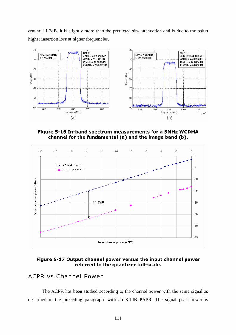
111
around 11.7dB. It is slightly more than the predicted sinc attenuation and is due to the balun
higher insertion loss at higher frequencies.
Figure 5-16 In-band spectrum measurements for a 5MHz WCDMA channel for the fundamental (a) and the image band (b).
Figure 5-17 Output channel power versus the input channel power referred to the quantizer full-scale.
ACPR vs Channel Power
The ACPR has been studied according to the channel power with the same signal as
described in the preceding paragraph, with an 8.1dB PAPR. The signal peak power is

112
considered for the full-scale reference. The ACPR is plotted on Figure 5-18 for the 650MHz
and 1.95GHz bands. The maximum ACPR is 53.6dB and 44.3dB, respectively. These
measured values meet the UMTS requirements (33/43dB for adjacent and alternate channels)
even in the 1.95GHz attenuated image band.
Figure 5-18 ACPR vs Channel Power for adjacent and alternate channels around fundamental and image bands.

113
SNDR vs Channel Power
Figure 5-19 650MHz fundamental band : (a) Signal and in-band noise power on 30MHz related to the input channel power (b) SNDR on 30MHz
vs input power.
For Signal-to-Noise and Distortion Ratio (SNDR) study, the input is a 5MHz sine
wave. The amplitude of this sine wave is referred to the quantizer full-scale. 0dBFS refers to
the peak power of the maximum coded sine wave.
The SNDR is plotted on Figure 5-19b. The peak value is 53.6dB over a 30Mz
bandwidth for an input power of -4.4dBFS. In system simulations, the SNDR peak value
appeared for a -3dBFS input sine wave. Measurements show that the delta-sigma modulators
saturate for an input sine wave power higher than -4.4dBFS. On Figure 5-19a, the peak output
power is 1.09dBm in a single-ended configuration and is obtained for -3dBFS, although the
SNDR is already degraded. For a differential output, the peak output power is 3dB higher,
thus reaching 3.1dBm. For input channel powers lower than -4.4dBFS, the noise floor is equal
to -129.5dBm/Hz. For higher values, the in-band noise begins to rise, thus prematurely
degrading the SNDR value.

114
Figure 5-20 1.95GHz image band : (a) Signal and in-band noise power on 30MHz related to the input channel power (b) SNDR on 30MHz vs input
power.
Figure 5-20 shows the same plots for the 1.95GHz image band. The peak SNDR is
40.8dB over a 30MHz bandwidth for a -4.4dBFS input power. The peak output power is -
8.59dBm into a differential load and for an input power of -2dBFS. It is to note that the noise
floor is equal to -129.4dBm/HZ and is almost the same as in the fundamental band (what was
not the case when the ACPR has been studied). Furthermore, one can observe a different
slope for low and high input powers in the SNDR plot, as well as in the signal power plot.
These particularities, degrading the image band SNDR and system linearity, have not been
explained yet and need further investigations.
EVM measurements
Error Vector Magnitude (EVM) has been measured with the Agilent Modulation
Analyzer. Constellations have been acquired and the EVM for the 3.84MS/s RRC filtered
QPSK downconverted signal is measured to 1.24% for the 650MHz band and 3.42% for the
1.95GHz band (Figure 5-21). For comparison, in UMTS, the EVM specification is 17.5% for
output powers higher than -20dBm. Typical performance of analog transmitters is 7 to 8%.
A study of the EVM parameter has been made related to the channel power. Results
are presented on Figure 5-22. For the 650MHz band, the EVM stays under 2% down to -
10dBFS. The EVM for the image band is higher and stays around 6%. For input powers lower
than -20dBFS, the EVM could not have been measured due to the sensitivity of the input
stages of the instrument, which cannot handle such low signals. Further measurements must

115
be made with an amplifier before the instrument input stage in order to check if the EVM
stays low or really increases. For high input powers, the EVM degrades due to the saturation
of the ∆Σ core system.
Figure 5-21 IQ constellations for the fundamental (right) and image band (left). This plot leads to the EVM measurement.
Figure 5-22 EVM versus the input channel power
Output Jitter
Output jitter has been measured to investigate the degradation of the analog output
spectrum measurement, compared with the digital data stream analysis presented before. The

116
2.6GS/s output signal has been applied to an Agilent Infiniium DSO 81204A oscilloscope to
characterize it. The eye diagram of this signal is plotted on Figure 5-23. It shows a mean jitter
of 13.24psRMS, an eye width of about 300ps (for a 385ps period) and an eye height of 636mV.
According to non-idealities simulations presented in a previous section, we can conclude that
the main contribution to the observed analog in-band noise is the output signal jitter. It has
two possible sources. First, it comes from the phase noise on the main clock, which travels all
along the chip and is surely disturbed by surrounded active switching area. Next, the supply
voltage varies on the output stages, what can affect the switching threshold of the inverters
and thus the switching instant. One more time, an emphasis is made on the cleanliness of the
design of output stages and clock blocks.
Figure 5-23 Eye diagram of the 2.6GS/s output
Summary of measurements with a 2.6GHz main clock
Above measurements have been summarized in Table 5-1. The power consumption
has been measured for the whole chip, due to the single 1V power supply. The relative
contributions of the output stages and the core have been evaluated during first prototype
measurements, where the output buffers consumption has been evaluated separately.

117
2.6GHz clock
650MHz channel
1.95GHz channel (image)
ACPR (5MHz wide channel) 53.6dB 44.3dB
Max Channel Power -3.9dBm -15.8dBm
EVM 1.24% 3.42%
Output jitter 13.2psRMS
SNDR (BW = 30MHz) 53.6dB 40.3dB
In-band noise floor -129.5dBm/Hz -129.4dBm/Hz
Peak output power 3.1dBm -8.59dBm
total 69mW (1V)
output stages 39mW Power
consumption core 2 × 15mW
Table 5-1 Summary of measurements with a 2.6GHz clock
5.2.3.3 Measurements at other frequencies
Each parameter measured previously for the 2.6GHz main clock frequency will be
studied here for clock frequencies from 200MHz to 4GHz, thus addressing bands from
50MHz to 1GHz (from 1GHz to 3GHz for the image band) with a proportional bandwidth.
The input power is fixed for these measurements and we can assume that the power behavior
will be similar for all frequencies.
Power consumption
The power provided to the 50Ω resistive loads is equal to 20mW under a 1V supply
voltage. In fact, the two differential outputs deliver a 1V delta-sigma signal, whose average
voltage is 0.5V. It leads to 10mA of current consumption into the 50Ω load and consequently
to a global power consumption of 20mW for the two differential outputs.
Power consumption has been plotted on Figure 5-24 for each clock frequency between
100MHz and 4GHz when the circuit is in its active state. This supply voltage has to be
adjusted, so that the chip is operating properly and is shown in this figure for each frequency.
The power consumption has been measured and then scaled to a 1V supply voltage reference
for comparison and tendency analysis. It shows that the switching losses increase with the
frequency with a nearly 20mW/GHz slope.

118
Figure 5-24 Chip total power consumption as a function of the clock frequency
Evolution of ACPR
Figure 5-25 ACPR versus carrier frequencies for fundamental bands
The ACPR has been measured for different working frequencies with a -3dBFS
channel. Considering the fundamental bands, Figure 5-25 shows the ACPR for alternate and
adjacent channels as a function of the carrier frequency. The channel width is proportional to

119
the carrier frequency and equals to 3.84MHz for the 650MHz center carrier frequency. The
measured ACPR stays higher than 50dB for every frequency, except for the 1GHz carrier
frequency. The UMTS requirements for ACPR are 33 and 43dB for adjacent and alternate
channels. These specifications are fully completed.
Figure 5-26 shows a similar plot with the ACPR measurement extended to the image
band. As explained before, the ACPR is attenuated by about 8dB for image bands. The
measured values are around 43dB from 1GHz to 3GHz. They are at the limit of the 43dB
requirement for alternate channels, sometimes a little worse. The measured difference for
particular frequencies could be explained by a very sensitive device to every parameters of the
test setup (supply voltage, clock frequency and DC bias and even perturbations brought by the
digital inputs).
Figure 5-26 ACPR versus carrier frequencies for fundamental and image bands

120
Evolution of SNDR
Figure 5-27 Measured SNDR for different main clock frequencies
The SNDR has been measured with a sine wave at a few MHz (its frequency is
proportional to the clock frequency) and with a -6dBFS power. It is plotted in Figure 5-27. The
SNDR is calculated by measuring the ratio of the signal power to the noise power inside a
bandwidth relative to the sampling frequency. It shows an almost constant SNDR value,
except for two measurement points (at 1.4 and 4GHz) on which the noise level was
particularly high when measured. The high noise floor for the 4GHz clock frequency (1GHz
carrier frequency) could explain the degraded ACPR measured at this frequency in the
preceding section. Measurement errors could be responsible for the isolated measured value at
1.4GHz.

121
Evolution of EVM
Figure 5-28 Measured EVM as a function of the main clock frequency
The Error Vector Magnitude is plotted on Figure 5-28 as a function of the main clock
frequency. It has been measured for the fundamental bands with a frequency-relative
bandwidth QPSK modulated channel at a -3dBFS peak power. From 200MHz to 4GHz, the
EVM stays under 6%, most of the time around 2%. It degrades itself at particular frequencies
around 1GHz, probably due to measurement incertitude. At clock frequencies near 4GHz, the
EVM also increases, thus reflecting the previous observations.

122
Evolution of the channel power
Figure 5-29 Output channel power versus the main clock frequency
The channel power has been acquired and measured with the Agilent Modulation
Analyzer. This output channel power is not constant with the frequency. It varies by about
4dB, depending upon the working frequency, as shown on Figure 5-29. The maximum output
power is around -2dBm. Around a 1.2GHz and a 3GHz clock frequency, the output channel
power degrades to -5.5dBm. These variations are hard to explain. The inserted balun could
influence the channel power by amplitude and phase mismatch and insertion losses. A
characterization of the implemented balun must be performed in order to define if the balun is
really responsible for these variations or if other aspects interfere.

123
Evolution of the jitter
Figure 5-30 Data and clock jitter versus the main clock frequency
The output jitter is responsible for a huge part of the degradation on the output signal
in-band spectrum. This analog behavior has been measured by acquiring the output data
stream on an Agilent Infiniium oscilloscope. Figure 5-30 plots the measured values for
different frequencies. First, the jitter has been measured when the circuit is in active state with
input data. The data jitter increases with the clock frequency. It goes from 6psRMS at 1GHz to
almost 15psRMS at 3.5GHz. When the circuit is in the reset state, outputting a periodical signal
at a fourth of the clock frequency, the jitter is, for every frequency, around 2psRMS. This
demonstrates that the output data jitter does not come from the clock path. It rather comes
either from the disturbances of the digital core switching activity on the clock signal or from
the data-dependent behavior of the mixer and output stages.
Summary of measurements
Performances described for the 2.6GHz clock frequency remains relatively constant
for other frequencies operation, up to 4GHz. ACPR measurements show values above 50dB
for fundamental bands and around 43dB for image bands. It fulfils UMTS ACPR
requirements for most frequencies. SNDR stays around 50dB, although the chip performances
degrade for a 4GHz clock frequency. EVM stays under 6% for all frequencies when measured

124
with the maximum channel power. The whole chip power consumption is of course increasing
with the frequency with a 20mW/GHz slope.
However, channel power and jitter varies with the frequency. More investigations are
needed to explain the channel power variations. The jitter increases with the frequency, which
is not surprising, due to the interactions between the digital core and the clock signals.
5.2.4 Comparison with similar works
This work [10]
Max Clock Frequency 4GHz clock 700MHz clock
Max Carrier Frequency 1GHz channel 3GHz channel
(image) 175MHz channel
Max Adjacent ACPR (5MHz wide channel)
55dB @ 500MHz clock
44.5dB @ 2.4GHz clock
50.26dB
Max Alternate ACPR (5MHz wide channel)
57.2dB @ 500MHz clock
47dB @ 2.4GHz clock
40.27dB
Total Power Consumption 25mW (1V) @ 700MHz clock 69mW (1V) @ 2.6GHz clock
139mW (1.5V)
Total Silicon Area 3.2mm² 5.2mm²
Process 90nm CMOS (GP) 130nm CMOS
Table 5-2 Comparison with similar works
The only similar work has been reported in 2004 [10], but for IF frequencies. The
clock frequency was 700MHz for a 175MHz IF carrier frequency. The ACPR measured for a
5MHz WCDMA channel are 50.26dB and 40.27dB, respectively for adjacent and alternate
channels. In their system, the ∆Σ modulators bandwidth is pretty much the same as the
channel bandwidth, what explains the bad value for alternate channel ACPR. The quantization
noise is already increasing due to the limited bandwidth. It employs a current output and the
full-scale current is 11.5mA. The die area of the chip is 5.2mm² and it consumes 139mW
with a 1.5V supply.
Our work offers a higher working frequency, a larger bandwidth, a better ACPR for
the fundamental band, a lower power consumption and a smaller die area, as compared in
Table 5-2.
125
5.3 Conclusion
Two 90nm CMOS chips has been designed and fabricated from a STMicroelectronics
process for demonstrating the digital transmitter proposed concept based on ∆Σ modulation.
The first chip was not functional but brings valuable information for a redesign. The second
chip has shown functionality up to a 4GHz main clock frequency, thus addressing a 1GHz
maximum carrier frequency (or 3GHz if the image band is considered). Measured
performances fulfill requirements for most standards, such as UMTS. Performances in the
image band are a little lower, due to the inherent sinc attenuation.
For a 2.6GHz clock frequency, the measured ACPR is around 53dB for a 5MHz wide
channel and the channel output power is -3.9dBm. The SNDR is about 53dB over a 30 MHz
bandwidth. The EVM is lower than 2%. The chip consumes 69mW on a 1V supply voltage
and occupies a 3.2mm² die are (0.15mm² for the active area).
Those parameters remain almost constant for working frequencies from 200MHz to
4GHz.
The designed chip settles the state-of-the-art in ∆Σ-based digital RF signal generation
in terms of working frequency. The measurement results obtained on this prototype are high
enough for this kind of digital chip to replace existing analog implementations in a near
future.


127
CONCLUSION
For the field of mobile communications, a digital RF transmitter using ∆Σ modulation
has been demonstrated. A prototype 90nm CMOS chip has been designed, which fulfils
requirements for standards such as UMTS. One of the potential advantages of a 1-bit coded
digital RF signal is the ability to use class-S switched power amplifiers having a very high
efficiency.
Parallel works
The architecture demonstrated here is the first reported transmitter chain using 1-bit
digital ∆Σ .modulation working in the RF domain
Previously, as evoked in the state-of-the-art and measurement results, the nearest
implementation was made by Sommarek et al. [10] in 2004 for IF frequencies. The main
clock frequency is 700MHz and the obtained ACPR is 50.26/40.27dB for adjacent and
alternate channels. Our work marks a great advance in this field by moving the IF conversion
to RF frequencies.
Several works on transmitters from other research teams have been performed during
the three years of this thesis work. Two of those are of great interest [68, 69]. They explore a
different way by proposing a Digital-to-RF Conversion (DRFC). A multi-bit D-to-A converter
is merged with the mixer into the DRFC block.
In [68], 10-bit 307.2MS/s signals are applied to the DRFC. A 41/56dB ACPR is
obtained for WCDMA 5MHz channels and an output power of 25dBm. The EVM stays
below 2% over 60dB of control range.
In [69], a ∆Σ modulator is used to reduce the number of bits required in the DRFC to 3
bits. The ∆Σ modulator uses a second-order MASH structure and operates with a 2.5GS/s
sample rate. The MASH structure has been chosen for its simplicity and relatively short
critical path, only composed by a 12-bit adder. A passgate style adder with a differential
sense-amplifier flip-flop scheme has been designed. The aiming standard is mainly the
~500MHz bandwidth WLAN around 5GHz. The proposed concepts and the chip design are
very valuable and depict very good results. For comparison with our work, this
implementation only works with very simple ∆Σ modulator structures and is not compatible

128
with more complex structures, such as the 3rd-order zeros-optimized architecture used in this
thesis.
The DRFC structure is of great interest. However, one disadvantage of the DRFC
structure is that it requires on-chip matching. Moreover, this structure operates inherently in
current-mode, limiting at low voltage the maximum power that can be delivered to a load. In
particular, class-S amplification is incompatible with a current-mode output.
Reconfigurability
The proposed architecture opens a way for easy reconfigurability and flexibility. The
topology chosen for the ∆Σ modulators achieves a low and flat noise floor inside a band equal
to the clock frequency divided by 80. The possible configurabilities in this prototype are to
change the clock frequency value and the baseband signals to transmit. The frequency
planning has to be carefully investigated. Thus, every standard, up to a 3GHz center
frequency, can be addressed with the fundamental or image band, keeping in mind that the
image band offers worse performances.
For optimum reconfigurability, coefficients of the ∆Σ modulator should be
dynamically modified in order to place poles and zeros in a location appropriated to the
aiming standard. Investigations on coefficient reconfiguration have not been yet engaged but
should be stated as an objective for such an architecture.
We have recently begun to work on the possible location of zeros of the ∆Σ noise
transfer function [70]. We have imagined to increase the order of the ∆Σ modulators and to
place the added zeros in the band in which the noise constraints are the hardest to reach for
any given standard. Doing this would greatly relax the filter requirements. A method for
automatically placing poles and zeros for high-order ∆Σ modulators has been developed. An
example, shown in Figure C - 1, has been taken for a UMTS/DCS1800 reconfiguration.
The UMTS configuration clearly shows 3NTF zeros in the UMTS TX band (one of
them at the center band frequency and the two others near the band extremity). A zero has
been placed in the DCS TX band and another in the UMTS RX band. The zeros are
symmetrical around the carrier frequency. For the DCS1800 configuration, the clock
frequency has changed and 6 ∆Σ modulator coefficients are modified. It leads to the
placement of a zero on the DCS RX band (the other one is not in any specific band).

129
Figure C - 1 Output spectrum of a digital transmitter implemented with a configurable 5th order ∆Σ modulator in (a) UMTS configuration and (b)
DCS1800 configuration
Future directions
The chip developed in this thesis work is at a prototype state. Many enhancements
must be done in order to be able to replace advantageously the components in place and to
integrate it into a complete transmitter.
First of all, techniques for achieving very high-speed computations inside the ∆Σ
modulators have demonstrated a possible implementation with a 90nm CMOS process. Going
further with smaller and faster process will surely open a way to reduce the core complexity.
For example, investigations in 65nm have shown that, at transistor level design, the dynamic
logic could be replaced by simpler DPL static adders. For the same kind of application, the
latter logic style is, with a given technology, slower than dynamic logic style but is sufficient
when implemented with faster transistors. This modification heavily reduces complexity, as
the DLL 3-phase clock generation block becomes useless and the clock tree simpler.
Next, the filtering capability of such a digital RF stream, with huge out-of-band
quantization noise, remained to be proven. BAW filters are a good candidate to such an
application [32]. They are recently investigated inside the MOBILIS IST European project
[71]. The goal of the MOBILIS project is to enable digital multi-band handsets by developing
digital transmitter modules, combining a SoC digital integrated circuit (IC) with BAW filter
and SiP RF power module along with a power amplifier and BAW filter/duplexer. Main
challenges are the power handling capability and duration of BAW filters as well as the
impedance matching between switching-mode DACs and BAW filters.

130
Other ways of output filtering must be investigated. An interesting way is developed in
Axel Flament’s thesis [65]. Power combining is performed with transmission lines to replace
traditional power amplification stages. As it is a digital implementation, the proposed
structure enables a FIR filtering capability, which could greatly relax the constraints on
antenna filtering stages. This structure is in adequacy with a ∆Σ-based RF signal generator, as
it takes advantage of the high efficiency of switching power amplification.
All-digital transmitters with ∆Σ modulation are serious candidates to replace wireless
terminals analog front-end blocks. They offer reconfigurability, flexibility, robustness,
reduced power consumption, better efficiency and better integration. But many bottlenecks
still need to be overcome…

131
Bibliography
[1] H. Hiroshi and P. Ramjee, Simulation and Software Radio for Mobile Communications: Artech House, Inc., 2002.
[2] A. Gégout, "Software Radio ou Radio Logicielle," TDF White Paper, ref sav0061, 2002.
[3] C. Moy, et al., "Full Digital IF UMTS Transceiver for Future Software Radio Systems," in ERSA'2001 (first international conference on Engineering of Reconfigurable Systems and Algorithms) Las Vegas, USA, 2001.
[4] P. Asbeck, et al., "Digital signal processing - up to microwave frequencies," Microwave Theory and Techniques, IEEE Transactions on, vol. 50, pp. 900-909, 2002.
[5] P. M. Asbeck, L. E. Larson, and I. G. Galton, "Synergistic design of DSP and power amplifiers for wireless communications," IEEE Trans. on Microwave Theory and Techniques, vol. 49, pp. 2163-2169, 2001.
[6] M. Iwamoto, et al., "Bandpass delta-sigma class-S amplifier," Electronics Letters, vol. 36, pp. 1010-1012, 2000.
[7] R. Weigel, et al., "RF Transceiver Architectures for WCDMA Systems like UMTS: State of the Art and Future Trends," in Proc. of the Intern. Symp. on Acoustic Wave Devices for Future Mobile Communications Systems, Chiba, Japan, 2001, pp. 25-34.
[8] A. Bellaouar, et al., "Highly-integrated SiGe BiCMOS WCDMA transmitter IC," in Solid-State Circuits Conference, 2002. Digest of Technical Papers. ISSCC. 2002 IEEE International, 2002, pp. 238-463 vol.1.
[9] G. Brenna, et al., "A 2-GHz carrier leakage calibrated direct-conversion WCDMA transmitter in 0.13µm CMOS," Solid-State Circuits, IEEE Journal of, vol. 39, no. 8, pp. 1253-1262, 2004.
[10] J. Sommarek, et al., "A digital modulator with bandpass delta-sigma modulator," IEEE ESSCIRC, pp. 159-162, 2004.
[11] J. Vankka, et al., "A digital quadrature modulator with on-chip D/A converter," Solid-State Circuits, IEEE Journal of, vol. 38, pp. 1635-1642, 2003.
[12] V. W. Leung, L. E. Larson, and P. S. Gudem, "Digital-IF WCDMA handset transmitter IC in 0.25µm SiGe BiCMOS," Solid-State Circuits, IEEE Journal of, vol. 39, no. 12, pp. 2215-2225, 2004.
[13] I. Galton, "Delta-sigma data conversion in wireless transceivers," Microwave Theory and Techniques, IEEE Transactions on, vol. 50, pp. 302-315, 2002.
[14] J. Keyzer, et al., "Digital generation of RF signals for wireless communications with band-pass delta-sigma modulation," in Microwave Symposium Digest, 2001 IEEE MTT-S International, 2001, pp. 2127-2130 vol.3.

132
[15] A. Jayaraman, et al., "Linear high-efficiency microwave power amplifiers using bandpass delta-sigma modulators," IEEE Microwave and Guided Wave Letters, vol. 8, pp. 121-123, 1998.
[16] S. P. Stapleton, "High Efficiency RF Power Amplifiers Using Bandpass Delta-Sigma Modulators," Agilent Technologies Design Seminar.
[17] J. Sommarek, et al., "Comparison of different class-D power amplifier topologies for 1-bit band-pass delta-sigma D/A converters," in Norchip Conference, 2004. Proceedings, 2004, pp. 115-118.
[18] P. Midya, P. Wagh, and P. Rakers, "Quadrature integral noise shaping for generation of modulated RF signals," in Circuits and Systems, 2002. MWSCAS-2002. The 2002 45th Midwest Symposium on, 2002, pp. II-537-II-540 vol.2.
[19] P. Wagh, et al., "An all-digital universal RF transmitter," in Custom Integrated Circuits Conference, 2004. Proceedings of the IEEE 2004, 2004, pp. 549-552.
[20] R. B. Staszewski, et al., "All-digital TX frequency synthesizer and discrete-time receiver for Bluetooth radio in 130-nm CMOS," Solid-State Circuits, IEEE Journal of, vol. 39, pp. 2278-2291, 2004.
[21] ETSI, "Universal mobile telecommunications system (UMTS) : UE radio transmission and reception (FDD)," Technical Specification 125 101 v7.2.0, 2005.
[22] Ericsson, "Basic Concepts of WCDMA Radio Access Network," Ericsson White Paper, ref e207, 2001.
[23] R. Pickholtz, D. Schilling, and L. Milstein, "Theory of Spread-Spectrum Communications--A Tutorial," Communications, IEEE Transactions on, vol. 30, pp. 855-884, 1982.
[24] K. Gentile, "Fundamentals of digital quadrature modulation," in RF Design, 2003.
[25] "Report on specification of MEMS components and modules," in STREP MELODICT Deliverable D1.
[26] J. Gorisse, et al., "Report on the optimized WCDMA single-band transmitter architecture and component specifications," in FP6-STREP MOBILIS Deliverable D4.1, 2006.
[27] Y. Wang, "A class-S RF amplifier architecture with envelope delta-sigma modulation," in Radio and Wireless Conference, 2002. RAWCON 2002. IEEE, 2002, pp. 177-179.
[28] J. M. Rabaey, Digital Integrated Circuits: A Design Perspective, 1996.
[29] D. Galayko, "Etude de l'interférence entre symboles," IEMN/ISEN, CCI group, internal report 2004.

133
[30] J. F. Jensen, et al., "A 3.2-GHz second-order delta-sigma modulator implemented in InP HBT technology," Solid-State Circuits, IEEE Journal of, vol. 30, pp. 1119-1127, 1995.
[31] A. Flament, "Jitter study," IEMN/ISEN, CCI group, internal report 2005.
[32] J. F. Carpentier, et al., "A SiGe:C BiCMOS WCDMA zero-IF RF front-end using an above-IC BAW filter," in Solid-State Circuits Conference. Digest of Technical Papers. ISSCC. 2005 IEEE International, 2005, pp. 394-395 Vol. 1.
[33] A. Frappé, et al., "All-digital RF signal generation for software defined radio," in Circuits and Systems for Communications, ICCSC'06. Third IEEE International Conference on,, 2006, pp. 171-174.
[34] J. Vankka, et al., "A GSM/EDGE/WCDMA modulator with on-chip D/A converter for base stations," Circuits and Systems II: Analog and Digital Signal Processing, IEEE Transactions on, vol. 49, pp. 645-655, 2002.
[35] G. Aliftiras, "CDMA Waveform Generation for Digital Radios," Filtronic PLC White Paper, 2002.
[36] T. Ojanpera and R. Prasad, Wideband CDMA For Third Generation Mobile Communications: Universal Personal Communications: Artech House, Inc., 1998.
[37] M. Iglesias-Xamani, "Hybrid-Phase-Shift Keying Proposed for 3G Systems," in Wireless Systems Design. vol. 5, 2000, pp. 24-32.
[38] T. Yamazato, et al., "Performance evaluation of modified HPSK for wideband CDMA," in Spread Spectrum Techniques and Applications, IEEE Sixth International Symposium on, 2000, pp. 751-755 vol.2.
[39] R. Andraka, "A survey of CORDIC algorithms for FPGA based computers," in FPGA'98, Proceedings of the ACM/SIGDA 6th int. symp. on FPGA, Monterey, CA, 1998, pp. 191-200.
[40] S. R. Norsworthy, R. Schreier, and G. C. Temes, Delta-Sigma Data Converters Theory, Design, and Simulation, 1997.
[41] J. C. Candy and G. C. Temes, Oversampling Delta-Sigma Data Converters, Theory, Design, and Simulation: Wiley-IEEE Press, 1992.
[42] A. Sripad and D. Snyder, "A necessary and sufficient condition for quantization errors to be uniform and white," Acoustics, Speech, and Signal Processing, IEEE Transactions on, vol. 25, pp. 442-448, 1977.
[43] J. M. de la Rosa Utrera, "Modelado y Diseno de Modulatores Sigma Delta Paso de Banda para Communicaciones Digitales usando Circuitos de Corrientes en Commutacion," in Universidad de Sevilla, PhD Thesis, 2000.
[44] R. Kok and D. M. Weber, "On designing sigma-delta converter systems for class-D power amplifiers," in AFRICON, 1999 IEEE, 1999, pp. 715-718 vol.2.

134
[45] R. Schreier, "Delta-Sigma Toolbox," available on Mathworks website, 2001.
[46] C. Nagendra, M. J. Irwin, and R. M. Owens, "Area-time-power tradeoffs in parallel adders," Circuits and Systems II: Analog and Digital Signal Processing, IEEE Transactions on [see also Circuits and Systems II: Express Briefs, IEEE Transactions on], vol. 43, pp. 689-702, 1996.
[47] T. Sato, et al., "An 8.5-ns 112-b transmission gate adder with a conflict-free bypass circuit," Solid-State Circuits, IEEE Journal of, vol. 27, pp. 657-659, 1992.
[48] M. Suzuki, et al., "A 1.5-ns 32-b CMOS ALU in double pass-transistor logic," Solid-State Circuits, IEEE Journal of, vol. 28, pp. 1145-1151, 1993.
[49] S. Perri, P. Corsonello, and G. Cocorullo, "VLSI circuits for low-power high-speed asynchronous addition," Very Large Scale Integration (VLSI) Systems, IEEE Transactions on, vol. 10, pp. 608-613, 2002.
[50] CORE90GPSVT_1.00V_Databook: ST Central R&D Company Confidential, 2004.
[51] G. Jaberipur, B. Parhami, and M. Ghodsi, "Weighted bit-set encodings for redundant digit sets: theory and applications," in Signals, Systems and Computers. Conference Record of the Thirty-Sixth Asilomar Conference on, 2002, pp. 1629-1633 vol.2.
[52] H. R. Srinivas and K. K. Parhi, "A fast VLSI adder architecture," Solid-State Circuits, IEEE Journal of, vol. 27, pp. 761-767, 1992.
[53] Y. Dumonteix, "Optimisation des chemins de données arithmétiques par l'utilisation de plusieurs systèmes de numération," in ASIM Paris: Université Pierre et Marie Curie (UPMC), Thesis report, 2001.
[54] J. M. Muller, Arithmétique des ordinateurs: Masson, 1989.
[55] D. M. Hossack and J. I. Sewell, "The application of redundant number systems to digital sigma-delta modulators," in Circuits and Systems, 1994. ISCAS '94., 1994 IEEE International Symposium on, 1994, pp. 481-484 vol.2.
[56] A. Frappé, A. Kaiser, and A. Cathelin, "Procédé de traitement d'un signal numérique au sein d'un modulateur delta-sigma, et modulateur delta-sigma numérique correspondant," Patent B06-0749FR: STMicroelectronics and CNRS, 2006.
[57] A. Frappé, et al., "Design techniques for very-high speed digital delta-sigma modulators aimed at all-digital RF transmitters," in IEEE International Conference on Electronics, Circuits and Systems, Nice, France, 2006.
[58] A. Alvandpour, et al., "A 3.5GHz 32mW 150nm multiphase clock generator for high-performance microprocessors," in Solid-State Circuits Conference, 2003. Digest of Technical Papers. ISSCC. 2003 IEEE International, 2003, pp. 112-482 vol.1.
[59] K. Chulwoo, H. In-Chul, and K. Sung-Mo, "A low-power small-area +/-7.28-ps-jitter 1-GHz DLL-based clock generator," Solid-State Circuits, IEEE Journal of, vol. 37, pp. 1414-1420, 2002.

135
[60] T. Xanthopoulos, et al., "The design and analysis of the clock distribution network for a 1.2 GHz Alpha microprocessor," in Solid-State Circuits Conference, 2001. Digest of Technical Papers. ISSCC. 2001 IEEE International, 2001, pp. 402-403.
[61] D. Eckerbert, L. J. Svensson, and P. Larsson-Edefors, "A mixed-mode delay-locked-loop architecture," in Computer Design, 2003. Proceedings. 21st International Conference on, 2003, pp. 261-263.
[62] N. R. Mahapatra, A. Tareen, and S. V. Garimella, "Comparison and analysis of delay elements," in Circuits and Systems, 2002. MWSCAS-2002. The 2002 45th Midwest Symposium on, 2002, pp. II-473-II-476 vol.2.
[63] M. Yongsam, et al., "An all-analog multiphase delay-locked loop using a replica delay line for wide-range operation and low-jitter performance," Solid-State Circuits, IEEE Journal of, vol. 35, pp. 377-384, 2000.
[64] A. Flament, et al., "Convertisseur numérique analogique 1 bit à 7,8Gech/s pour émetteurs RF numériques en technologie CMOS 90nm," in Traitement Analogiqe de l'Information, du Signal et ses Applications, TAISA, Strasbourg, 2006.
[65] A. Flament, "Combineur de puissance à lignes de transmission et filtre FIR reconfigurable pour applications radio-fréquences," in Université des Sciences et Technologies de Lille, France, PhD Thesis, to be published, 2008.
[66] Tektronix, AWG410/AWG420/AWG430 200MS/s Arbitrary Waveform Generator User Manual.
[67] "Mini-Circuits TC1-1-13M Data Sheet," http://www.minicircuits.com/products/transformers_sm_g.html#config_g.
[68] P. Eloranta, et al., "A WCDMA Transmitter in 0.13µm CMOS Using Direct-Digital RF Modulator," ISSCC Dig. Tech. Papers, pp. 340-341, 2007.
[69] A. Jerng and C. G. Sodini, "A Wideband Delta-Sigma Digital-RF Modulator for High Data Rate Transmitters," IEEE J. Solid-State Circuits, vol. 42, pp. 1710-1722, 2007.
[70] C. Nsiala Nzéza, et al., "Reconfigurable Digital Delta-Sigma Modulator Synthesis for Digital Wireless Transmitters," in IEEE European Conference on Circuit Theory and Design, Sevilla, Spain, 2007.
[71] "IST MOBILIS European Project Web Site," www.ist-mobilis.org.

136

I
Résumé en français
Le domaine d’application de ce travail concerne les communications mobiles et plus
particulièrement les architectures de transmission. Ce travail de recherche introduit une
architecture de transmetteur numérique qui permettrait de remplacer avantageusement les
solutions matérielles actuelles. Cette architecture tire profit de la modulation ∆Σ d’un signal
suréchantillonné qui permet de quantifier un mot numérique sur 1 bit sans toutefois perdre
l’information utile dans le bruit de quantification apporté. La très haute cadence de cette partie
numérique met en avant des limitations qui sont surmontées par des techniques innovantes.
Un circuit prototype en 90nm CMOS a été développé pour démontrer le concept proposé.
L’organisation des parties est la suivante. Dans une première partie, la notion de radio
logicielle est abordée. Un état de l’art sur les architectures d’émission est effectué pour
replacer l’architecture proposée dans son contexte. Enfin, les principales spécifications du
standard UMTS sont données. Ce standard sera pris comme exemple, dans un premier temps,
pour la conception du circuit. La deuxième partie décrit l’architecture du transmetteur
numérique proposé, en axant sur les choix architecturaux. La troisième partie est centrée sur
le modulateur ∆Σ et décrit toutes les techniques utilisées afin de pouvoir faire fonctionner ce
système numérique à cadence rapide. Le quatrième chapitre décrit la conception du
transmetteur au niveau transistor. Chaque bloc est décrit en mettant en avant le schéma et le
layout utilisé. Le dernier chapitre est consacré aux mesures sur les circuits prototypes. Les
composants de tests et les résultats de mesures sont détaillés et comparés avec la littérature.
Ce résumé en français détaille, de façon concise et rapide le contenu de chaque
chapitre en anglais, en mettant en avant les concepts proposés, les limitations rencontrées et
comment elles ont été surmontées.
Contexte
Radio logicielle
Le concept de radio logicielle imagine un transmetteur pour les communications
mobiles comme étant un bloc de traitement de signal multifonctions et totalement
reconfigurable. Il pourrait se placer juste devant un convertisseur numérique-analogique et

II
l’antenne d’émission, afin de fournir le signal RF désiré selon le standard sélectionné (Figure
1-1). Devant la profusion de standards existants ou à venir (GSM, UMTS, Wi-Fi, Wimax, 4G,
etc…), ce genre de terminal mobile universel serait une révolution.
Etat de l’art sur les architectures de transmetteurs
La tendance est de numériser progressivement la chaîne d’émission afin de se
rapprocher du concept de radio logicielle. Traditionnellement, les architectures d’émission
sont entièrement analogiques (Figure 1-3 et Figure 1-4). La conversion N/A est réalisée en
bande de base. On distingue deux implémentations possibles selon que la transposition en RF
se fait en une ou deux étapes. Ces structures sont respectivement appelées homodynes et
hétérodynes. Récemment, des architectures utilisant une conversion N/A aux fréquences
intermédiaires (IF) ont été proposées (Figure 1-5). Elles sont principalement basées sur des
modulateurs ∆Σ et des mélangeurs numériques en quadrature. Enfin, ce concept est étendu
aux fréquences RF (Figure 1-8). Cela permet d’utiliser des amplificateurs de puissance
commutés, offrant une très bonne efficacité. A ce jour, aucune implémentation aux
radiofréquences n’est reportée. Le concept est démontré dans la littérature théoriquement et
par des simulations. Le but du travail présenté ici est de démontrer par un prototype la
faisabilité d’une telle architecture et sa possible implémentation dans des technologies CMOS
nanométriques.
Spécifications du standard UMTS
Nous nous intéressons ici à la couche physique de l’UMTS dont les spécifications sont
données par l’ETSI. En émission, l’UMTS utilise une bande de 60MHz située entre 1,92 et
1,98GHz. L’UMTS utilise une technique d’accès multiples par codage (CDMA).
L’information est étalée sur des canaux larges de 5MHz, d’où le nom de WCDMA (W pour
Wideband). Les spécifications qui nous intéressent sont les suivantes :
• Le masque d’émission spectrale en bande (Table 1-1 et Figure 1-13).
• Les valeurs d’ACLR (Adjacent Channel Leakage Ratio) pour les canaux
adjacents et alternatifs (Table 1-2). Ces valeurs sont respectivement égales à 33
et 43dB.
• Les émissions parasites qui définissent la puissance maximale à l’antenne pour
certaines bandes de fréquence (Figure 1-14 et Table 1-3). Les contraintes

III
proviennent principalement des bandes dédiées à la réception UMTS et
DCS1800 ainsi que des bandes GSM.
• La valeur d’EVM dont le maximum est de 17,5%.
Architecture du transmetteur numérique
Choix de l’architecture
Le but de cette architecture est de fournir un signal 1 bit suréchantillonné contenant
l’information du signal RF à un amplificateur de puissance commuté. L’architecture
envisagée est constituée autour d’un modulateur ∆Σ et d’un transposeur numérique en
quadrature. Le modulateur ∆Σ quantifie le signal numérique en une séquence à cadence rapide
sur 1 bit. Le bruit de quantification apporté est repoussé en dehors de la bande utile. La
transposition numérique permet de placer le signal autour de la fréquence RF porteuse voulue.
Deux architectures sont envisageables (Figure 2-5). La première utilise un modulateur
∆Σ passe-bande suivant une transposition numérique du signal. La seconde utilise deux
modulateurs passe-bas sur les voies I et Q, suivis d’une transposition numérique sur un seul
bit. La seconde solution a été retenue car elle permet de simplifier fortement le bloc de
transposition RF et de réduire par deux la cadence d’échantillonnage des modulateurs ∆Σ.
La cadence d’échantillonnage Fs du bloc de transposition est égal à 4 fois la fréquence
centrale du standard (1,95GHz × 4 = 7,8Géch/s). Celle des modulateurs ∆Σ est alors de la
moitié (3,9Géch/s). Pour rentrer dans les spécifications dynamiques du standard, les
modulateurs conçus sont du troisième ordre avec un rapport de suréchantillonnage de 40
(bande passante de 100MHz).
Transposition numérique RF 1 bit
En choisissant une configuration passe-bas pour les modulateurs ∆Σ, on a largement
simplifié l’opération de transposition RF, puisqu’on ne travaille plus que sur un seul bit. Les
données de sortie des modulateurs ∆Σ des voies I et Q sont multipliées numériquement par un
sinus et un cosinus à la fréquence centrale, échantillonnés à Fs. Cette multiplication
numérique revient à faire une opération de multiplexage entre les voies I et Q, telle que la
sortie est la séquence constituée par [ ]QIQI ,,, . Cette opération devient très simple à réaliser
sur un faible nombre de bits.

IV
Par contre, un problème de synchronisation des deux voies apparaît. En effet, les
modulateurs fonctionnent de manière synchrone et les voies I et Q ne sont plus en quadrature
lors du multiplexage. Une image du canal apparaît alors de l’autre côté de la porteuse (Figure
2-7). Pour éviter ce phénomène, une interpolation linéaire est constamment réalisée sur la
voie Q avant les modulateurs ∆Σ.
Architecture proposée
L’architecture proposée est présentée sur la Figure 2-16. Elle est basée sur les deux
modulateurs ∆Σ et le bloc de transposition RF décrit plus haut. D’autres blocs sont
nécessaires dans cette chaîne de transmission. Ces blocs sont les suivants :
• Un traitement en bande de base qui met en forme les signaux d’entrée selon le
standard considéré.
• Un bloc de conversion de cadence qui réalise une conversion non entière et
suréchantillonne les signaux jusqu’à 2/sF .
• Les deux modulateurs ∆Σ passe-bas qui transforment le signal numérique
d’entrée en un signal 1 bit, dont le bruit de quantification est repoussé hors
bande.
• Un bloc de transposition numérique RF sur 1 bit.
• Un amplificateur de puissance commuté.
• Un filtre d’antenne
Le choix a été fait de considérer non pas un canal UMTS, mais la totalité de la bande
du standard (soit 60MHz), afin d’avoir un bruit relativement uniforme dans la bande passante.
Le traitement en bande de base
Le traitement en bande de base est constitué de blocs permettant la mise en forme du
signal (Figure 2-17). A partir des données à transmettre, le signal est étalé sur 3,84MHz et
embrouillé afin d’avoir son propre code. Ensuite, un filtre à cosinus surélevé avec un roll-off
de 0,22 permet de limiter la bande occupée par le canal à 5MHz. Des filtres demi-bandes
permettent de suréchantillonner le signal afin d’atteindre une cadence de 122,88Méch/s.
Finalement, un algorithme numérique de CORDIC est utilisé pour placer le canal de 5MHz
sur une sous-porteuse dans la bande de 60MHz du standard. Le signal de sortie généré est
présenté sur la Fig 2-10.
V
La conversion de cadence
La cadence du signal en bande de base est dépendante de la cadence symbole
(3,84Méch/s). C’est un multiple de cette cadence (122,88Méch/s, ici). Par contre, la cadence à
l’entrée des modulateurs ∆Σ est de 3,9Géch/s. Pour palier au fait que le rapport entre ces deux
fréquences soit non entier, on peut rajouter un décalage sur la fréquence de sous-porteuse, en
bande de base, selon la Table 2-2.
Ensuite, le signal doit être suréchantillonné par 32 (Figure 2-20). Des simulations ont
montré qu’un premier filtre FIR demi-bande très efficace permet de s’affranchir du filtrage
des étages suivants. Ces étages deviennent de simples interpolateurs d’ordre 1, relativement
faciles à implémenter. En effet, les images résultantes de ce manque de filtrage seront noyées
dans le bruit de quantification hors-bande généré par les modulateurs ∆Σ.
Les modulateurs ΔΣ numériques
Un modulateur ∆Σ est composé d’un quantificateur, assimilable à une source de bruit
blanc, et d’une boucle de contre-réaction. Ce système possède des fonctions de transfert
différentes pour le signal et pour le bruit de quantification. Pour le signal, la fonction de
transfert est plate dans la bande passante, tandis que pour le bruit, elle présente une fonction
de filtrage qui atténue le bruit en bande et le repousse en dehors de la bande utile. On peut
ainsi coder, sur très peu de bits mais avec une très bonne dynamique, des signaux limités en
bande.
L’architecture des modulateurs passe-bas du troisième ordre est présentée sur la Figure
2-23. Elle a la particularité d’avoir une boucle de retour permettant de placer des zéros aux
extrémités de la bande considérée, permettant ainsi d’élargir la bande passante et d’avoir un
bruit de quantification relativement plat dans celle-ci (Figure 2-24).
Les performance simulées indiquent un ACPR d’environ 75dB pour un canal de
5MHz et un SNDR de 76dB (13 bits efficaces).
L’amplificateur de puissance et les filtres d’antenne
L’amplificateur de puissance est ici considéré comme un convertisseur N/A. Sa
topologie est relativement simple, puisqu’elle consiste en une chaîne d’inverseurs de
dimensions croissantes (Figure 2-11). L’efficacité théorique d’un tel étage est de 100%, mais

VI
des pertes lors des commutations et de la puissance dissipée statiquement ou dynamiquement
réduisent cette efficacité.
D’autres non-idéalités perturbent le signal de sortie. L’asymétrie des fronts est
compensée par une structure de sortie différentielle. Par contre, le jitter sur le signal de sortie
dégrade le spectre en augmentant le bruit dans la bande.
Le filtre d’antenne doit être capable d’atténuer le bruit hors bande, notamment dans les
bandes de réception d’autres standards. Des technologies telles que les filtres BAW pourraient
permettre un filtrage efficace de ce genre de signal.
Conception système du modulateur ∆Σ
A partir de la structure du modulateur ∆Σ définie précédemment, des optimisations
sont nécessaires pour permettre de réaliser les opérations logiques à haute cadence
(3,9Géchs/s) à l’intérieur du système. Dans un premier temps, l’accumulateur présent dans
l’architecture précédente sera remplacé par un intégrateur (Figure 3-2). Ensuite, les
coefficients du modulateur vont être arrondis à la puissance de deux la plus proche, selon la
Table 3-1, afin que ces opérations ne prennent aucun temps de calcul. En effet, elles
consisteront en de simples décalages des bits des signaux internes. Les performances
dynamiques sont peu affectées. Le SNDR est dégradé d’environ 3dB tandis que l’ACLR est
de 74,7dB et 72,2dB, respectivement pour les canaux adjacents et alternatifs.
Utilisation de l’arithmétique redondante
Le chemin critique est constitué par un additionneur à 4 entrées précédant le 2ème
registre (Figure 3-4 et Figure 3-5). En utilisant une architecture classique en complément à 2,
le chemin critique est réduit à deux additions successives sur environ 16 bits. La cadence
d’échantillonnage visée est de 3,9Géch/s, soit environ 250ps de période. Ce qui laisse moins
de 125ps pour une addition 16bits (en omettant le temps de propagation des bascules, qui sera
bien sûr non négligeable).
En utilisant des additionneurs à retenue bondissante (RCA (Figure 3-7)), le temps de
propagation est environ égal au nombre de bits multiplié par le temps de propagation unitaire
d’un additionneur complet (FA), ce qui est bien supérieur au temps disponible. Des structures
à anticipation de retenue permettent d’améliorer le temps de calcul total. Malheureusement,

VII
même avec des portes logiques rapides (en logique DPL, par exemple (Figure 3-9)), la
contrainte de temps ne peut être respectée.
L’utilisation d’une arithmétique redondante, pour remplacer l’arithmétique en
complément à 2 permettrait d’atteindre la cadence désirée. En arithmétique redondante de
type Borrow-Save (BS), chaque signal sur N bits est codé par 2 x N bits, la moitié codant pour
du positif et l’autre moitié pour du négatif (Figure 3-10). Ainsi, un nombre donné peut être
codé de plusieurs façons différentes, d’où le nom de « redondant ». Ce codage permet de
réaliser des additions en temps constant, sans propagation de retenue, ce qui nous avantage
dans le type d’architecture implémentée.
On construit, à partir de cellules FA traditionnelles, des cellules appelées signed-FA,
qui constitueront les blocs de base de l’architecture (Figure 3-12). Chaque bloc est détaillé
dans les figures suivantes (Figure 3-17 à Figure 3-21). Le chemin critique est maintenant
composé d’au maximum trois cellules FA successives. Les performances du modulateur sont
quasiment identiques aux performances précédentes.
Quantification non exacte et pré-évaluation du signal de sortie
Le quantificateur de sortie est sur deux niveaux (1 bit) et définit donc le signe du
signal entrant. Malheureusement, avec un nombre codé en arithmétique redondante, on a
difficilement accès à cette information. En effet, déterminer le signe d’un nombre codé en
arithmétique redondante revient à propager une retenue à travers tous ses bits. On a déplacé le
problème du chemin critique sur le quantificateur.
Une étude des performances du modulateur en fonction du nombre de bits pris en
compte dans la quantification a permis de mettre en évidence que les paramètres dynamiques
sont très peu dégradés si on réduit le nombre de bits du quantificateur (Figure 3-24). Dans
notre cas, nous avons pu réduire ce nombre à 3 bits. De plus, une étude logique a montré, dans
l’architecture particulière implémentée ici, que le signe pouvait être déterminé par une
fonction à 3 entrées. Les performances sont très légèrement dégradés (Table 3-5). L’ACLR
est de 68,8 et 67,4dB pour des offsets de 5 et 10MHz.
Même si la fonction logique du quantificateur a été réduite, elle occupe un certain
temps de calcul. L’idée a été de traiter cette opération en parallèle avec le dernier étage
(Figure 3-26), en pré-évaluant le signe du signal de sortie.

VIII
Conception circuit du transmetteur numérique
Description du circuit intégré
Le circuit intégré contient les blocs de suréchantillonnage par 16, les modulateurs ∆Σ,
le bloc de transposition numérique et les buffers de préamplification. A cela s’ajoutent les
blocs de génération (basé sur une DLL) et de distribution des horloges, ainsi que les blocs de
contrôle (Figure 4-1 et Figure 4-2).
Le premier circuit prototype a été conçu dans une technologie CMOS 90nm de
STMicroelectronics. Le layout est présenté sur la Figure 4-3. Il mesure 3×1mm² et comporte
96 pads. On trouve 13 pads d’entrée numériques pour les voies I et Q sur les parties hautes et
basses du pad ring, ainsi que des sorties numériques parallélisées. A gauche se trouve l’entrée
d’horloge et à droite les pads de sortie RF. Un second prototype a ensuite été conçu dans la
même technologie afin de corriger les erreurs et d’améliorer le fonctionnement du circuit. Les
modifications apportées sont détaillées dans le chapitre suivant.
Le bloc de conversion de cadence
Le bloc de conversion de cadence a pour rôle de suréchantillonner le signal entrant de
243,75Méch/s jusque 3,9Géch/s. Ce suréchantillonnage est du premier ordre et est donc
facilement construit avec des bascules cadencées avec des horloges à ces fréquences. Deux
schémas d’horloges ont été utilisés pour chacun des prototypes (Figure 4-4 et Figure 4-5).
Dans le premier prototype, le circuit intégré génère l’horloge à 250MHz à partir de celle à
4GHz et les instruments sont contrôlés avec cette horloge. Dans le deuxième prototype, c’est
l’inverse qui est utilisé. L’horloge à 250MHz est amenée de l’extérieure et resynchronisée en
interne. Sur la voie Q, le circuit permettant l’interpolation linéaire, pour éviter la mauvaise
synchronisation des 2 voies, est présenté sur la Figure 4-7.
Les bascules utilisées dans ce bloc sont des bascules dynamiques utilisant un seul front
d’horloge (TSPCFF). Ces bascules ont été créées pour pouvoir fonctionner à haute cadence
grâce à un système de précharge et d’évaluation. Son schéma et son layout sont présentés sur
la Figure 4-8. Son mécanisme est expliqué sur la Figure 4-9.
La conception du circuit du modulateur ΔΣ numérique
Dans le chapitre précédent, on a montré qu’avec l’arithmétique redondante, 3 cellules
FA au maximum doivent être traitées pendant une période d’horloge. L’idée a donc été de

IX
diviser chaque période en trois parties, ou couches. Pour la conception circuit des
modulateurs, la logique dynamique a été identifiée comme la plus rapide et la seule pouvant,
en CMOS 90nm, permettre au système de rentrer dans la période désirée. L’utilisation de ce
type de logique évite de recourir à des bascules. Par contre, on a besoin d’une horloge pour
chaque bloc. Nous avons donc besoin de trois horloges (une pour chaque couche), chacune
déphasée d’un tiers de période par rapport à l’autre. Une DLL, détaillée plus loin, permettra
de générer ces horloges. L’arrangement des cellules est présenté sur la Figure 4-12.
Les cellules FA en logique dynamique sont totalement différentielles et sont basées sur
deux étages (Figure 4-13). Un premier qui aura les fonctions de précharge et d’évaluation,
selon la polarité de l’horloge. Le deuxième sera un inverseur trois-états, le troisième état étant
une fonction de maintien de l’information en sortie. Chaque cellule fonctionne donc en moins
de 83ps (tiers de période).
Ces cellules sont très sensibles à la non-différentialité des entrées, du fait que le
système soit rebouclé. Ainsi, un circuit d’initialisation a dû être intégré au circuit des cellules
de base, afin de pouvoir démarrer correctement. Sur le premier prototype, les sorties ont été
placées dans un état différentiel en tirant les potentiels à travers un transistor vers leurs
valeurs respectives (Figure 4-15). Cette technique ne fonctionne que sur une gamme de
fréquences donnée, puisque la commande d’initialisation doit arriver à un moment opportun
par rapport aux horloges. Sur le second prototype, un circuit, comprenant des transistors
couplés, a été développé afin de garantir la différentialité des signaux et un fonctionnement à
toutes les fréquences (Figure 4-16). Le layout du cœur numérique du circuit est présentée sur
les Figure 4-17 et Figure 4-18.
Génération et distribution des horloges
Une DLL est utilisée pour générer 3 horloges déphasées à partir d’une horloge
principale (Figure 4-19). Elle consiste en des éléments de retard contrôlables et d’un détecteur
de phase qui fournit une information sur le déphasage de l’horloge de sortie (360°) par rapport
à celle d’entrée. Cette information est traitée par une pompe de charge qui contrôle la valeur
des retards.
La ligne à retards est composée d’inverseurs enchaînés, qui comprennent deux
transistors supplémentaires (un NMOS et un PMOS) dans leur chemin de charge et de
décharge (Figure 4-20). Ainsi, en fonction de la tension appliquée sur ces transistors,
l’inverseur sera plus ou moins rapide. Le détecteur de phase est basé sur une bascule RS. La
X
pompe de charge utilise une capacité sur laquelle elle vient ajouter ou prélever une certaine
quantité de charge, définie par le courant utilisé (100µA, ici) dans la pompe de charge. On
obtient en simulation de très bonnes caractéristiques (Table 4-1).
Mélangeur numérique et étage de sortie
La structure du mélangeur numérique est basée sur des portes de transmission
pipelinées, afin de réaliser l’opération de multiplexage (Figure 4-26). Une attention
particulière a été portée sur le fait que les chemins de données ne devaient pas dépendre des
données traitées. Pour cela une bascule a été insérée dans l’architecture (Figure 4-27). L’étage
de sortie est composé d’une ligne de buffers croissants. Un diagramme de l’œil de la sortie
RF, obtenu en simulation, est présenté sur la Figure 4-28.
Résultats expérimentaux
Premier circuit prototype
Le matériel de test pour le premier circuit est décrit, afin de pouvoir d’une part,
analyser le spectre de la sortie analogique et d’autre part, acquérir les données numériques de
sortie (Figure 5-1 et Figure 5-2). Les signaux sont générés sur un générateur arbitraire (AWG
420). Des cartes basées sur des FPGA ont été fabriquées pour suréchantillonner ces signaux
jusqu’à 250Méch/s.
Le circuit intégré a été bondé sur un substrat de 24×12mm² sur des pistes de cuivre
large de 50µm et espacées de 50µm (Figure 5-3). Ce substrat est ensuite soudé sur une carte
fille abritant tous les composants utiles à l’alimentation et aux contrôles. Deux connecteurs la
relient à une carte mère abritant les FPGA (Figure 5-4).
Les mesures sur ce premier prototype n’ont pas été fructueuses. Le circuit n’est pas
fonctionnel à haute cadence car de larges variations sont présentes sur les alimentations, dues
aux pics de courant à travers les bondings (Figure 5-5 et Figure 5-6). Malheureusement, à
cause du système d’initialisation, le système n’est pas fonctionnel à plus basse fréquence. Le
fonctionnement du cœur n’a donc pas pu être testé. Par contre, nous avons pu tirer des
informations sur les aspects du circuit à retravailler et quelques mesures sur l’étage de sortie,
notamment au niveau de sa consommation (Figure 5-7 et Figure 5-8).

XI
Deuxième circuit prototype : changements et protocoles de tests
Les principaux changements apportés sont les suivants :
• L’alimentation a été retravaillée (regroupement de toutes les alimentations,
placement judicieux des pads d’alimentation et de masse) et les pads ont été
espacés afin de faciliter l’étape d’assemblage.
• Des capacités de découplage ont été ajoutées sur le circuit intégré.
• Le système d’initialisation a été revu (décrit dans une partie précédente).
Les protocoles de test sont sensiblement identiques à ceux du premier circuit, à la
différence près que les sorties numériques ont été supprimées (Figure 5-11).
Deuxième circuit : résultats de mesure pour une horloge à 2.6GHz
Le circuit fonctionne comme désiré jusqu’à une fréquence d’horloge de 4GHz (au lieu
des 7,8GHz prévus). Ainsi, le circuit peut adresser une bande passante de 50MHz jusqu’à une
fréquence porteuse de 1GHz (voire 3GHz si la bande image est considérée ; on observe dans
ce cas une atténuation due au sinus cardinal). Le signal de sortie RF a été acquis avec un
oscilloscope numérique et le signal, une fois traité comme un signal numérique, a révélé la
fonction de transfert attendue pour les modulateurs ∆Σ (Figure 5-13).
Avec une fréquence d’horloge à 2,6GHz, une bande autour de 650MHz a pu être
adressée (1,95GHz pour la bande image). Le signal d’entrée est soit un canal WCDMA de
5MHz de large modulé en QPSK, soit une sinusoïde placée aux alentours de 5MHz. L’ACPR,
le SNDR et l’EVM ont été étudiés en fonction de la puissance du canal ou de la sinusoïde.
Dans le tableau suivant sont regroupées les caractéristiques mesurées, dont toutes les figures
sont données (Figure 5-14 à Figure 5-23). Le circuit mesuré rentre dans les spécifications
pour le standard UMTS.

XII
Horloge à 2,6GHz
Canal à 650MHz
Canal à 1,95GHz (image)
ACPR (canal de 5MHz de large) 53,6dB 44,3dB
Puissance max du canal -3,9dBm -15,8dBm
EVM 1,24% 3,42%
Jitter de sortie 13,2psRMS
SNDR (BW = 30MHz) 53,6dB 40,3dB
Bruit en bande -129,5dBm/Hz -129,4dBm/Hz
Puissance de sortie en pic 3,1dBm -8,59dBm
total 69mW (1V)
Etage de sortie 39mW Consommation
Coeur 2 × 15mW
Deuxième circuit : résultats de mesure en fonction de la fréquence
La consommation du circuit augmente en fonction de la fréquence avec une pente
d’environ 20mW/GHz (Figure 5-24). L’ACPR, ainsi que le SNDR, mesurés à différentes
fréquences restent relativement identiques aux valeurs mesurées précédemment (Figure 5-25à
Figure 5-27). L’EVM reste toujours inférieur à 6% (Figure 5-28). Par contre, la puissance du
canal varie fortement avec la fréquence. La variation va jusqu’à 4dB (Figure 5-29).
L’explication n’est pas encore claire mais cela provient probablement du balun utilisée pour la
conversion différentielle vers single-ended. Le jitter de sortie augmente avec la fréquence,
comme attendu à cause des perturbations des éléments logiques sur les alimentations et les
chemins d’horloge. Pour la plupart des fréquences, le système rentre dans les spécifications
du standard UMTS, qui est un des plus contraignants.
Une comparaison est effectuée entre ce travail et un travail réalisé sur une architecture
identique mais fonctionnant en fréquences intermédiaires (Table 5-2). Cette comparaison
montre une nette avancée de nos travaux, surtout en termes de fréquence de fonctionnement.
Conclusion
Pour des applications de communications mobiles, un transmetteur numérique RF
utilisant la modulation ∆Σ a été proposé et démontré. Un prototype en technologie 90nm
CMOS a été développé, qui respecte les spécifications de la plupart des standards, tels que

XIII
l’UMTS. Un des avantages potentiels d’un signal RF numérique codé sur 1 bit est la
possibilité d’utiliser un amplificateur de puissance commuté, ayant une grande efficacité.
L’architecture démontrée ici est la première chaîne d’émission utilisant une modulation ∆Σ
sur 1 bit reportée dans la littérature pour des fréquences RF.
Les directions futures concernent principalement la reconfigurabilité dynamique du
système pour différents standards (DCS1800, etc…) et l’implémentation de cette architecture
dans des technologies plus poussées (65nm, par exemple). En effet, les techniques
développées ici pourront être implémentés avec une conception circuit plus simple. Par
exemple, la logique dynamique, contraignante en termes de gestion des horloges, pourra être
avantageusement remplacée par de la logique statique rapide comme la DPL, grâce à un
process technologique plus rapide.
Dans un futur proche, le filtrage devra aussi être étudié. Des filtres BAW pouvant
répondre à la demande de filtrage sont actuellement étudiés dans le projet européen
MOBILIS. D’autres techniques pouvant réduire les contraintes de filtrage sont aussi à l’étude,
comme par exemple, un filtrage numérique sur le signal de sortie (thèse d’Axel Flament).
Les transmetteurs numériques à base de modulateurs ∆Σ sont de bons candidats pour
remplacer avantageusement les architectures analogiques actuelles des transmetteurs mobiles.
Ils peuvent offrir de la reconfigurabilité, de la flexibilité, de la robustesse, une consommation
réduite, une meilleure efficacité et une meilleure intégration. Mais beaucoup de verrous
technologiques doivent encore être surmontés…