Embed Size (px)
Citation preview
Giant magnetoresistance in ferromagnet/organic semiconductor/ferromagnet heterojunctions
Jung-Woo Yoo,1,2 H. W. Jang,3 V. N. Prigodin,1 C. Kao,2 C. B. Eom,3 and A. J. Epstein1,2
1Department of Physics, The Ohio State University, Columbus, Ohio 43210-1117, USA2Department of Chemistry, The Ohio State University, Columbus, Ohio 43210-1173, USA
3Department of Materials Science and Engineering, University of Wisconsin–Madison, Madison, Wisconsin 53706, USA�Received 6 April 2009; revised manuscript received 26 October 2009; published 30 November 2009�
We report the spin injection and transport in ferromagnet/organic semiconductor/ferromagnet �FM/OSC/FM�heterojunctions using rubrene �C42H28� as an organic semiconductor spacer. For completeness of our study,both tunneling magnetoresistance �TMR� and giant magnetoresistance �GMR� were studied by varying thethickness of the rubrene layer �5–30 nm�. A thorough study of the device characteristics reveals spin-polarizedcarrier injection into and subsequent transport through the OSC layer. When the thickness of the rubrene layersare beyond the tunneling limit, the device currents are limited by carrier injection and bulk transport. Thecarrier injection is well described with phonon-assisted field emission. The behavior of GMR in response tobias field and temperature shows significant differences from that of TMR.
DOI: 10.1103/PhysRevB.80.205207 PACS number�s�: 72.25.Hg, 72.25.Dc, 73.40.Mr, 75.47.De
I. INTRODUCTION
The study of spin injection, transport, and dynamics insemiconductors, known as “spintronics,”1 has received grow-ing attention over the last decade. Observation of magnetore-sistance �MR� in magnetic trilayers is a common approach tostudy spin injection and transport. Here, the magnetic trilayeris comprised of soft and hard magnets separated by a non-magnetic spacer to allow parallel �on� and antiparallel �off�alignments of the magnetic layers. Then, MR, defined asMR�%�=100� �RAP−RP� /RP, relies on spin-dependent scat-tering at the interfaces and spin-polarized carrier transport inthe spacer.
The spintronic applications of organic semiconductors�OSCs� were motivated by long spin lifetime in OSCs due tolow spin-orbit coupling and weak hyperfine interaction.2–17
The early report of spin valve effects utilizing a thick layer��100 nm� of tris�8-hydroxyquinolinato�aluminum �Alq3�as a spacer in vertical devices3 has brought considerable at-tention to organic semiconductor spintronics. But, low de-vice resistance, weak temperature �T� dependence of I-Vcurves, and low-bias �Vb� MR have brought critiques9–11 ar-guing that the reported MR �Ref. 3� originates from tunnel-ing magnetoresistance �TMR� in locally thin areas of theOSC layer9,10 as shown for the magnetic tunnel junction us-ing thin layers of Alq3 and rubrene �C42H28�.7,8 In this paper,we use the term giant magnetoresistance �GMR� referring tomagnetoresistance induced by the injection and transport ofspin-polarized carriers through the nonmagnetic spacers in-stead of tunneling through thin insulating barriers.
Organic semiconductors typically have an energy gap ofmore than 2 eV �e.g., rubrene �2.3 eV; Alq3 �2.8 eV� be-tween highest occupied molecular orbital �HOMO� and low-est unoccupied molecular orbital �LUMO� levels. Thus, thesematerials are closer to insulators than to conventional inor-ganic semiconductors. The charge transport in the HOMO/LUMO levels is provided by phonon-assisted hopping as theorbital overlap between the adjacent molecules is small anddriven by the strong electric field in the organic electronicdevices. In accordance with the previous criticisms9–11 con-
cerning the observation of GMR, the amorphous OSC filmspaced spin valve devices should have �a� extremely highjunction resistance at low bias �� several mV� and low Tdue to large energy gap, �b� strong T-dependent junction re-sistance due to activated carrier injection at the interface andactivated carrier transport in the bulk, and �c� strong nonlin-ear I-V curves with substantial T dependence due to carrierinjection and space charge effect.
Recent studies of the spin diffusion in OSC layers usingmuon spin rotation14 and photoemission15 techniques demon-strated spin injection into an OSC layers. However, the esti-mated effective spin diffusion length in OSC layers is muchshorter ��s�10 nm� �Refs. 14 and 15� in comparison to theprevious reports2,3,13 of the MR using “�100 nm” of amor-phous OSC spacers. In short, the observation of GMR is stillcontroversial and the understanding of spin injection andtransport in OSC layer is still lacking due to lack of compre-hensive device characteristic study.18 In this paper, wepresent the underlying nature of how carriers are mediatedthrough the OSC films depending on bias, temperature, andOSC film thickness and show clear distinction between TMRand GMR and provide direct evidence of electrical spin in-jection and detection in OSC-spaced spin valve devices.
Though the OSC materials hold promise for their longspin lifetimes, injection and transport of spin-polarized car-riers in OSC films meet significant obstacles. There are typi-cally large band offsets between the Fermi level of typicalferromagnetic metals and the HOMO and LUMO levels ofthe OSCs. The dipolar barrier at the metal/OSC interfacecreates defect states and may interfere with spin-polarizedcarrier injection.7 Even when the efficient spin injection intothe HOMO/LUMO levels of an OSC is achieved, hoppingtransport in amorphous small molecule films associated withphonon interaction may undermine efficient spin transport,especially at high T. Finally, there is a conductivity mismatchissue in applying highly resistive materials as the spin trans-porting spacer.19,20 However, the flexibility of organic chem-istry has potential for significant improvement of efficientspin injection and transport in organic semiconductors. De-spite the available wide range of materials and novel pro-
PHYSICAL REVIEW B 80, 205207 �2009�
1098-0121/2009/80�20�/205207�9� ©2009 The American Physical Society205207-1
cessing techniques applied in other organic electronics re-search, the spintronic applications of OSC materials havebeen focused on exploiting amorphous small molecule filmsindicating that the research in this field is still in its infancy.The evolution of this field will rely on developing desirablematerials and processing techniques for the improvement ofinterfacial quality and efficient spin diffusion in organicspacers.
In this work, we fabricated spin valve structures �Fig.1�a�� using La2/3Sr1/3MnO3 �LSMO� and Fe as an anode anda cathode, respectively, and rubrene as the OSC spacer. Toimprove interfacial quality between the LSMO and rubrene,we applied a thin layer �1.2 nm� of LaAlO3 �LAO�. Theobserved TMR in magnetic tunnel junction using a thin ru-brene layer �5 nm� displays spin-conserved tunnelingthrough the hybrid barrier �LAO�1.2 nm�/rubrene�5 nm��, asreported by Shim et al.8 The T- and Vb-dependent behaviorof TMR in our devices is similar to the previously reportedGMR behavior in organic-based spin valves using LSMO,3,13
in agreement with a early suggestion by Xu et al.9 As thethickness of the rubrene layer increases, devices are limitedby carrier injection and transport. For intermediate thickness�d�20 nm�, the carrier injection described by thermionicfield emission controls the device current. Applying high biasis needed to have viable device current as well as to observeMR. The observed GMR for the devices with intermediatethickness of rubrene layer shows spin-polarized carrier injec-tion into, and subsequent transport through the rubrene layer.The responses of GMR in our devices to bias field and T
show clear differences from that of TMR through the thinhybrid �oxide/OSC� layer.
This paper is organized as follows. In the following Sec.II, we present our device fabrication procedure. We then pro-vide background for tunneling vs carrier injection and trans-port in organic spin valves. The variation in MR in thin hy-brid barrier device in response to temperature and bias fieldis presented in Sec. IV. In Sec. V, we display T- andVb-dependent characteristics in our thick rubrene spaced de-vices. We analyze these experimental results in terms ofphonon-assisted field emission. We then present the tempera-ture and bias field dependences of MRs in our thick rubrenespaced devices in Sec. VI. Finally, Sec. VII is for the sum-mary and conclusions.
II. DEVICE FABRICATION
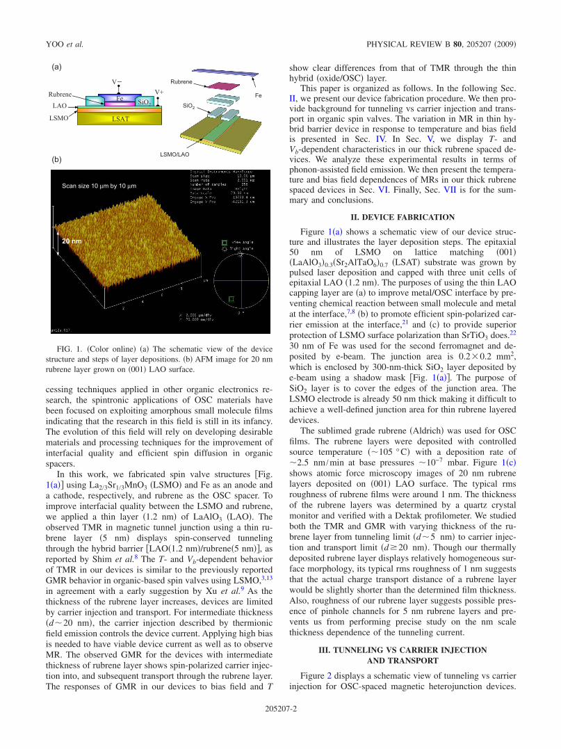
Figure 1�a� shows a schematic view of our device struc-ture and illustrates the layer deposition steps. The epitaxial50 nm of LSMO on lattice matching �001��LaAlO3�0.3�Sr2AlTaO6�0.7 �LSAT� substrate was grown bypulsed laser deposition and capped with three unit cells ofepitaxial LAO �1.2 nm�. The purposes of using the thin LAOcapping layer are �a� to improve metal/OSC interface by pre-venting chemical reaction between small molecule and metalat the interface,7,8 �b� to promote efficient spin-polarized car-rier emission at the interface,21 and �c� to provide superiorprotection of LSMO surface polarization than SrTiO3 does.22
30 nm of Fe was used for the second ferromagnet and de-posited by e-beam. The junction area is 0.2�0.2 mm2,which is enclosed by 300-nm-thick SiO2 layer deposited bye-beam using a shadow mask �Fig. 1�a��. The purpose ofSiO2 layer is to cover the edges of the junction area. TheLSMO electrode is already 50 nm thick making it difficult toachieve a well-defined junction area for thin rubrene layereddevices.
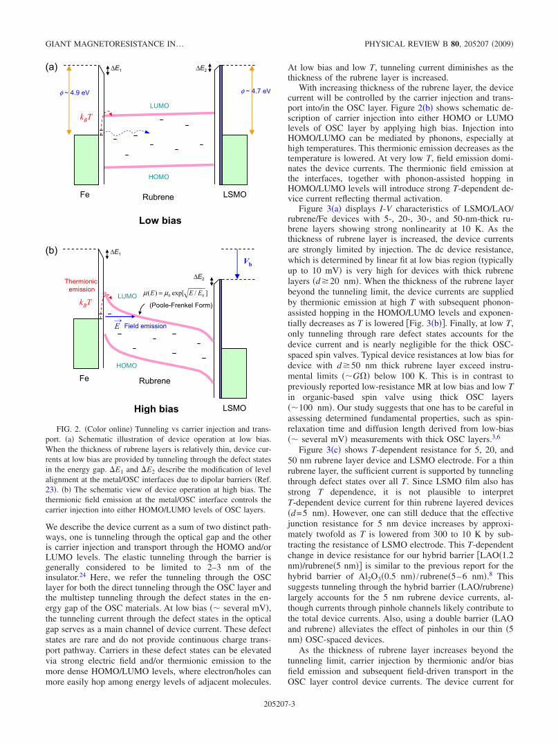
The sublimed grade rubrene �Aldrich� was used for OSCfilms. The rubrene layers were deposited with controlledsource temperature ��105 °C� with a deposition rate of�2.5 nm /min at base pressures �10−7 mbar. Figure 1�c�shows atomic force microscopy images of 20 nm rubrenelayers deposited on �001� LAO surface. The typical rmsroughness of rubrene films were around 1 nm. The thicknessof the rubrene layers was determined by a quartz crystalmonitor and verified with a Dektak profilometer. We studiedboth the TMR and GMR with varying thickness of the ru-brene layer from tunneling limit �d�5 nm� to carrier injec-tion and transport limit �d�20 nm�. Though our thermallydeposited rubrene layer displays relatively homogeneous sur-face morphology, its typical rms roughness of 1 nm suggeststhat the actual charge transport distance of a rubrene layerwould be slightly shorter than the determined film thickness.Also, roughness of our rubrene layer suggests possible pres-ence of pinhole channels for 5 nm rubrene layers and pre-vents us from performing precise study on the nm scalethickness dependence of the tunneling current.
III. TUNNELING VS CARRIER INJECTIONAND TRANSPORT
Figure 2 displays a schematic view of tunneling vs carrierinjection for OSC-spaced magnetic heterojunction devices.
(a)
(b)LSMO/LAO
SiO2
Rubrene
Fe
Scan size 10 µm by 10 µm
20 nm
Fe
LSAT
SiO2
LSMO
Rubrene
LAO
V+V−
FIG. 1. �Color online� �a� The schematic view of the devicestructure and steps of layer depositions. �b� AFM image for 20 nmrubrene layer grown on �001� LAO surface.
YOO et al. PHYSICAL REVIEW B 80, 205207 �2009�
205207-2
We describe the device current as a sum of two distinct path-ways, one is tunneling through the optical gap and the otheris carrier injection and transport through the HOMO and/orLUMO levels. The elastic tunneling through the barrier isgenerally considered to be limited to 2–3 nm of theinsulator.24 Here, we refer the tunneling through the OSClayer for both the direct tunneling through the OSC layer andthe multistep tunneling through the defect states in the en-ergy gap of the OSC materials. At low bias �� several mV�,the tunneling current through the defect states in the opticalgap serves as a main channel of device current. These defectstates are rare and do not provide continuous charge trans-port pathway. Carriers in these defect states can be elevatedvia strong electric field and/or thermionic emission to themore dense HOMO/LUMO levels, where electron/holes canmore easily hop among energy levels of adjacent molecules.
At low bias and low T, tunneling current diminishes as thethickness of the rubrene layer is increased.
With increasing thickness of the rubrene layer, the devicecurrent will be controlled by the carrier injection and trans-port into/in the OSC layer. Figure 2�b� shows schematic de-scription of carrier injection into either HOMO or LUMOlevels of OSC layer by applying high bias. Injection intoHOMO/LUMO can be mediated by phonons, especially athigh temperatures. This thermionic emission decreases as thetemperature is lowered. At very low T, field emission domi-nates the device currents. The thermionic field emission atthe interfaces, together with phonon-assisted hopping inHOMO/LUMO levels will introduce strong T-dependent de-vice current reflecting thermal activation.
Figure 3�a� displays I-V characteristics of LSMO/LAO/rubrene/Fe devices with 5-, 20-, 30-, and 50-nm-thick ru-brene layers showing strong nonlinearity at 10 K. As thethickness of rubrene layer is increased, the device currentsare strongly limited by injection. The dc device resistance,which is determined by linear fit at low bias region �typicallyup to 10 mV� is very high for devices with thick rubrenelayers �d�20 nm�. When the thickness of the rubrene layerbeyond the tunneling limit, the device currents are suppliedby thermionic emission at high T with subsequent phonon-assisted hopping in the HOMO/LUMO levels and exponen-tially decreases as T is lowered �Fig. 3�b��. Finally, at low T,only tunneling through rare defect states accounts for thedevice current and is nearly negligible for the thick OSC-spaced spin valves. Typical device resistances at low bias fordevice with d�50 nm thick rubrene layer exceed instru-mental limits ��G�� below 100 K. This is in contrast topreviously reported low-resistance MR at low bias and low Tin organic-based spin valve using thick OSC layers��100 nm�. Our study suggests that one has to be careful inassessing determined fundamental properties, such as spin-relaxation time and diffusion length derived from low-bias�� several mV� measurements with thick OSC layers.3,6
Figure 3�c� shows T-dependent resistance for 5, 20, and50 nm rubrene layer device and LSMO electrode. For a thinrubrene layer, the sufficient current is supported by tunnelingthrough defect states over all T. Since LSMO film also hasstrong T dependence, it is not plausible to interpretT-dependent device current for thin rubrene layered devices�d=5 nm�. However, one can still deduce that the effectivejunction resistance for 5 nm device increases by approxi-mately twofold as T is lowered from 300 to 10 K by sub-tracting the resistance of LSMO electrode. This T-dependentchange in device resistance for our hybrid barrier �LAO�1.2nm�/rubrene�5 nm�� is similar to the previous report for thehybrid barrier of Al2O3�0.5 nm� / rubrene�5–6 nm�.8 Thissuggests tunneling through the hybrid barrier �LAO/rubrene�largely accounts for the 5 nm rubrene device currents, al-though currents through pinhole channels likely contribute tothe total device currents. Also, using a double barrier �LAOand rubrene� alleviates the effect of pinholes in our thin �5nm� OSC-spaced devices.
As the thickness of rubrene layer increases beyond thetunneling limit, carrier injection by thermionic and/or biasfield emission and subsequent field-driven transport in theOSC layer control device currents. The device current for
(a)
Low bias
(b)
Fe
LSMO
Rubrene
HOMO
LUMOkBT
∆E2
∆E1Vb
Field emission→E
Thermionicemission ]/exp[)( 00 EEE µµ =
(Poole-Frenkel Form)
High bias
φ ~ 4.9 eV
Fe LSMORubrene
φ ~ 4.7 eV
HOMO
LUMO
kBT
∆E2∆E1
FIG. 2. �Color online� Tunneling vs carrier injection and trans-port. �a� Schematic illustration of device operation at low bias.When the thickness of rubrene layers is relatively thin, device cur-rents at low bias are provided by tunneling through the defect statesin the energy gap. �E1 and �E2 describe the modification of levelalignment at the metal/OSC interfaces due to dipolar barriers �Ref.23�. �b� The schematic view of device operation at high bias. Thethermionic field emission at the metal/OSC interface controls thecarrier injection into either HOMO/LUMO levels of OSC layers.
GIANT MAGNETORESISTANCE IN… PHYSICAL REVIEW B 80, 205207 �2009�
205207-3
thick OSC layers is strongly T dependent reflecting activa-tion processes and shows clear distinction from that of thinrubrene layered devices �Fig. 3�c��. Further detailed study onthe effect of thermionic field emission will be discussed inthe section of phonon-assisted field emission.
IV. TUNNELING MAGNETORESISTANCE IN FM/OSC/FMHETEROJUNCTIONS
Figure 4�a� displays I-V and dI /dV curves of a 5 nmrubrene device �LSMO�50 nm�/LAO�1.2 nm�/Rubrene�5nm�/Fe�30 nm�� at 10 K. The dI /dV was measured by thestandard lock-in technique. As discussed in previousliterature,7 the absence of a zero bias dip in the dI /dV curveindicates that hybrid barrier �LAO/rubrene� forms a well-defined tunneling barrier. Figure 4�b� displays magnetization�M� vs in-plane magnetic field �H� at 10 K for individual Fe�30 nm� and LSMO �50 nm on �001� LSAT� films recordedwith a superconducting quantum interference device�SQUID� magnetometer. MR curves of a 5 nm rubrene de-vice for Vb=10 mV and in-plane H at different T �10, 50,100, and 150 K� are displayed in Fig. 4�c�. The steps of theMR curves at each T well correspond to the T-dependentin-plane coercivity �Hc� for Fe and LSMO electrodes, asshown in Fig. 4�d�. The coercivity in Fig. 4�d� is determinedfrom the individual Fe �30 nm� and LSMO �50 nm� elec-trodes using a SQUID magnetometer. The substantial de-crease in MR as T is increased �see Fig. 6�d�� is attributed tothe T-dependent surface polarization of the LSMOelectrode.25 Similar T dependence of MR was commonly re-ported for various LSMO-based trilayers26 as well asorganic-based spin valve using LSMO electrodes.3,9,13,27,28
The bias dependence of MR curves for a typical 5 nmrubrene device at 10 K is presented in Fig. 4�e� for positivebiases and �f� for negative biases. Our TMR device exhibitspositive MR over all biases. The steps of MR curves for allbiases show excellent correspondence to the coercivities ofFe �30 nm� and LSMO �50 nm� electrodes. The MR vs Vb inFig. 4�g� was determined by the comparison of I-V curvesfor parallel �at H=500 Oe� and antiparallel �at H=−150 Oe� configurations of magnetic layers. The asymmet-ric MR for Vb is due to different electrodes �Fe, LSMO� andis similar to previous observations.3,9,27
The MR of our devices is positive over all T and Vb incontrast to previous reports, which showed negative MR inorganic-based spin valves.3,9,13,27 The difference between ourdevice and previously reported organic spin valves is that weused Fe instead of Co for the second ferromagnetic layer.Another possible origin of the negative MR in the spinvalves3,9,13,27 is the presence of pinhole channels. The ballis-tic current through nanoscale metallic contact could induceinversion from positive to negative MR as suggestedtheoretically29 and experimentally observed in LSMO-basedtrilayers.30
V. PHONON-ASSISTED FIELD EMISSION
With increasing thickness of rubrene layer, devices dis-play stronger nonlinear I-V curves and become injection lim-
Low bias Rdc
T (K)0 50 100 150 200 250 300
log 10Rdc
5
6
7
8
9
20 nm30 nm50 nm
I vs V
T = 10 K
Vb (V)0.0001 0.001 0.01 0.1 1 10
log 10I(A)
-11-10-9-8-7-6-5-4-3
5 nm20 nm30 nm50 nm Instrumental limit
(a)
R vs T
Vb = 0.1 V
T (K)0 50 100 150 200 250 300
log 10R(Ohm)
2
3
4
5
6
7
8
9
10
LSMOLAO/Rubrene 5 nmLAO/Rubrene 20 nmLAO/Rubrene 50 nm
Instrumental limit
(c)
(b)
FIG. 3. �Color online� �a� I-V curves of LSMO �50 nm�/LAO�1.2 nm�/Rubrene/Fe �30 nm� devices for the thickness of rubrenelayer d=5, 20, 30, and 50 nm at 10 K. Devices are injection limitedas d increases beyond tunneling limit. �b� Temperature dependenceof low bias �� several mV� Rdc showing exponential increase as Tis lowered. �c� Temperature dependence of resistance for LSMOelectrode and 5-, 20-, and 50-nm-thick rubrene devices at appliedbias of 0.1 V.
YOO et al. PHYSICAL REVIEW B 80, 205207 �2009�
205207-4
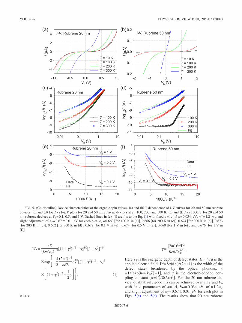
ited as shown in Figs. 5�a� and 5�b� for 20 and 50 nm ru-brene devices, respectively. Figures 5�c� and 5�d� show log Ivs log V plots for 20 and 50 nm rubrene devices. As the biasfield is increased, all curves for different T asymptote to thesame slope, which is a typical characteristic for charge injec-tion via field emission at metal/organic interface. Figures5�e� and 5�f� display T-dependent device resistances for 20and 50 nm rubrene devices, respectively. The noise at low Vband low T for 50 nm rubrene device is due to our instrumen-tal limit. The substantial increase in device current as T in-creases over 100 K can be attributed to active thermionicemission at the interface, once the device is limited by injec-tion. A similar T dependence of device conductance was pre-viously reported for an organic spin valve with a thin rubrene
layer.8 The LSMO resistance strongly decreases as T islowered2,28 but this resistance can be ignored as it is substan-tially smaller than the total device resistance for thick ru-brene layered devices �d�20 nm� �see Fig. 3�c��.
We describe the carrier injection in our spin valve deviceswith thermionic field emission at the metal/OSC interface asit was discussed in Sec. III. We adopt the theoretical modeldeveloped by Kiveris and Pipinys,31,32 which accounts formultiphonon activation of electrons together with field emis-sion from defect states at the interfaces to the conductionband for the metal/semiconductor junction. The phonon-assisted tunneling rate of electrons under the electric field atthe metal/semiconductor interface is as follows:31,32
MR vs Vb
Vb (V)-0.4 -0.2 0.0 0.2 0.4
MR(%)
0
4
8
12
16
20
T = 10 K
Hc vs T
Hc (Oe)-1000 -500 0 500 1000
T(K)
0
100
200
300
LSMOFe
MR vs H
H (Oe)-1000 -500 0 500 1000
MR(%)
-202468101214 10 K
50 K100 K150 K
M vs H
-1000 -500 0 500 1000
M(arb.units)
-1.0
-0.5
0.0
0.5
1.0
FeLSMO
T = 10 K
Vb = 10 mV
-0.1 0.0 0.1-20
-10
0
10
20
T = 10 K
I-VdI/dV
Vb (V)
I(µA)
40
45
50 dI/dV(arb.units)
MR vs H
H (Oe)-1500 -1000 -500 0 500 1000 1500
MR(%)
-202468101214
V = 1 mV10 mV50 mV100 mV150 mV200 mV300 mV
Negative Vb
T = 10 K
MR vs H
H (Oe)-1500 -1000 -500 0 500 1000 1500
MR(%)
-202468101214
V = 1 mV10 mV50 mV100 mV150 mV200 mV300 mV
Positive Vb
T = 10 K
(e)
(f)
(g)
(a)
(b)
(d)
(c)
FIG. 4. �Color online� Tunneling magnetoresistance of the hybrid magnetic tunnel junction. �a� I-V and dI /dV curves for magnetic tunneljunction of 5 nm rubrene device �LSMO�50 nm�/LAO�1.2 nm�/rubrene �5 nm�/Fe �30 nm��. �b� M vs H at 10 K for Fe �30 nm� and LSMO�50 nm� on LSAT�001� substrate. �c� MR curves of 5 nm rubrene device at T=10, 50, 100, and 150 K. �d� Hc vs T for Fe �30 nm� and LSMO�50 nm� magnetic layers recorded by SQUID. �e� Positive-bias dependence of MR curves for 5 nm rubrene device at 10 K. �f� Negative-biasdependence of MR curves for 5 nm rubrene device at 10 K. �g� The magnitude of MR as a function of Vb for 5 nm rubrene device. MR vsVb of 5 nm rubrene device at 10 K is determined by the difference in I-V curves between parallel �H=500 Oe� and antiparallel �H=−150 Oe� configurations for the 5 nm rubrene device.
GIANT MAGNETORESISTANCE IN… PHYSICAL REVIEW B 80, 205207 �2009�
205207-5
WT =eE
�8m��T�1/2 ��1 + �2�1/2 − ��1/2�1 + �2�−1/4
�exp�−4
3
�2m��1/2
eE�T
3/2��1 + �2�1/2 − ��2
���1 + �2�1/2 +1
2�� , �1�
where
� =�2m��1/22
8eE�T1/2 .
Here �T is the energetic depth of defect states, E=Vb /d is theapplied electric field, 2=8a���2�2n+1� is the width of thedefect states broadened by the optical phonons, n=1 / �exp�� /kBT�−1�, and a is the electron-phonon cou-pling constant �a=0
2 /8���2�. For the 20 nm rubrene de-vice, qualitatively good fits can be achieved over all T and Vbwith fixed parameters of a=1.4, �=0.034 eV, m�=1.2meand slight adjustment of �T=0.67�0.01 eV for each plot inFigs. 5�c� and 5�e�. The results show that 20 nm rubrene
Rubrene 20 nm
1000/T (K-1)0 5 10 15 20
log 10(I)(A)
-9
-8
-7
-6
-5
-4
DataFit
Vb = 0.1 V
Vb = 1 V
Vb = 0.5 V
Rubrene 50 nm
1000/T (K-1)0 5 10 15 20
log 10(I)(A)
-11
-10
-9
-8
-7
-6
-5
DataFit
Vb = 1 VVb = 0.5 VVb = 0.1 V
Rubrene 20 nm
Vb (V)0.01 0.1 1 10
log 10(I)(A)
-10
-9
-8
-7
-6
-5
-4
T = 100 KT = 200 KT = 300 KFit
Rubrene 50 nm
Vb (V)0.01 0.1 1 10
log 10(I)(A)
-11
-10
-9
-8
-7
-6
-5
100 K200 K300 KFit
(c)
(f)(e)
I-V, Rubrene 20 nm
Vb (V)-1.0 -0.5 0.0 0.5 1.0
I(µA)
-4
-2
0
2
4
T = 10 KT = 100 KT = 200 KT = 300 K
I-V, Rubrene 50 nm
Vb (V)-2 -1 0 1 2
I(µA)
-0.2
-0.1
0.0
0.1
0.2
T = 10 KT = 100 KT = 200 KT = 300 K
(a) (b)
(d)
FIG. 5. �Color online� Device characteristics of the organic spin valves. �a� and �b� T dependence of I-V curves for 20 and 50 nm rubrenedevices. �c� and �d� log I vs log V plots for 20 and 50 nm rubrene devices at T=100, 200, and 300 K. �e� and �f� I vs 1000 /T for 20 and 50nm rubrene devices at Vb=0.1, 0.5, and 1 V. Dashed lines in �c�–�f� are fits to the Eq. �1� with fixed a=1.4, �=0.034 eV, m�=1.2 me, andslight adjustment of �T=0.67�0.01 eV for each plot. �T=0.660 �for 100 K in �c��, 0.666 �for 200 K in �c��, 0.674 �for 300 K in �c��, 0.673�for 200 K in �d��, 0.662 �for 300 K in �d��, 0.678 �for 0.1 V in �e��, 0.674 �for 0.5 V in �e��, 0.660 �for 1 V in �e��, and 0.676 �for 1 V in�f��.
YOO et al. PHYSICAL REVIEW B 80, 205207 �2009�
205207-6
device currents are controlled by the carrier injection. MR ofthis device relies on the spin-dependent carrier injection atthe interface. However, the phonon-assisted tunneling, whichbecomes effective as T increases over 100 K, would affect onthe spin polarization of injected carriers.
Once the carriers are injected into an OSC layer, the mo-bility of electrons and holes also strongly rely on the appliedelectric field, for example, � 0 expE /E0 �Poole-Frenkelform�. Therefore, the slight deviation of the fitting at lowbias in Fig. 5�c� likely originates from the bulk resistance ofOSC, which becomes larger as T is lowered. As the thicknessof the rubrene layer is increased further, the carrier transport
in the bulk controls the device current. A larger deviation forour fitting to 50 nm rubrene device currents can be observedat low bias and low T as shown in Figs. 5�d� and 5�f�. Fittingfor 50 nm rubrene device was performed with the same fixedparameters of a=1.4, �=0.034 eV, m�=1.2me and a slightadjustment of �T=0.67�0.01 eV for each plot. Unlike in-terfacial barrier resistance, which nearly saturates below 100K for the relatively high bias, the phonon-assisted hoppingconductance in the OSC layer continues to decrease to low Tfollowing an exponential T dependence. This introduces astrong deviation of our fit to temperature-dependent deviceresistance for 50 nm rubrene layer as shown in Fig. 5�f� for
MR vs T
T (K)0 50 100 150 200 250 300
MR(%)
0
2
4
6
8
10
12
14Rubrene 5 nm,Vb = 10 mVRubrene 20 nm,Vb = 1 VRubrene 30 nm,Vb = 0.6 V
TMR
GMR
MR vs H, Rubrene 20 nm
Vb = 1 V
H (Oe)-1000 -500 0 500 1000
MR(%)
-2
0
2
4
6
8
10
10 K50 K100 K
T =
MR vs Vb
Vb (V)0.0 0.5 1.0 1.5 2.0
MR(%)
0
5
10
15
20
25
30Rubrene 20 nmRubrene 30 nm
T = 10 K
R vs HRubrene 20 nm
10 K
H (Oe)-2000 -1000 0 1000 2000
R(MOhm)
0.0
0.2
0.4
0.6
0.8
1.0
1.2
1.4
1.6
1.8
2.0
Vb = 0.4 V
Vb = 0.6 V
Vb = 0.8 V
Vb = 1 V
Vb = 1.2 V
(a) (b)
(c)
(d)
FIG. 6. �Color online� Giant magnetoresistance of the organic spin valves. �a� MR curves for 20 nm rubrene device for a different Vb at10 K. Device resistance decreases as Vb increases showing strong nonlinearity of I-V characteristic. �b� MR vs Vb plot for 20 and 30 nmrubrene devices at 10 K. �c� MR curves of 20 nm rubrene device for different T at Vb=1 V. The steps of MR well correspond to the Hc offerromagnetic layers at all T. �d� Comparison of T dependence of MR between TMR �5 nm rubrene device� and GMR �20 and 30 nm rubrenedevices�.
GIANT MAGNETORESISTANCE IN… PHYSICAL REVIEW B 80, 205207 �2009�
205207-7
T�100 K. In sum, for the thicker rubrene layer device �d�50 nm�, higher bias needs to be applied for efficient fieldemission as well as for supporting drift current �space-charge-limited regime, I�V2 /d3�. Hopping transport overlong distances and dephasing of charge-carrier spins in thebulk reduces the spin polarization of carriers.
VI. GIANT MAGNETORESISTANCE IN FM/OSC/FMHETEROJUNCTIONS
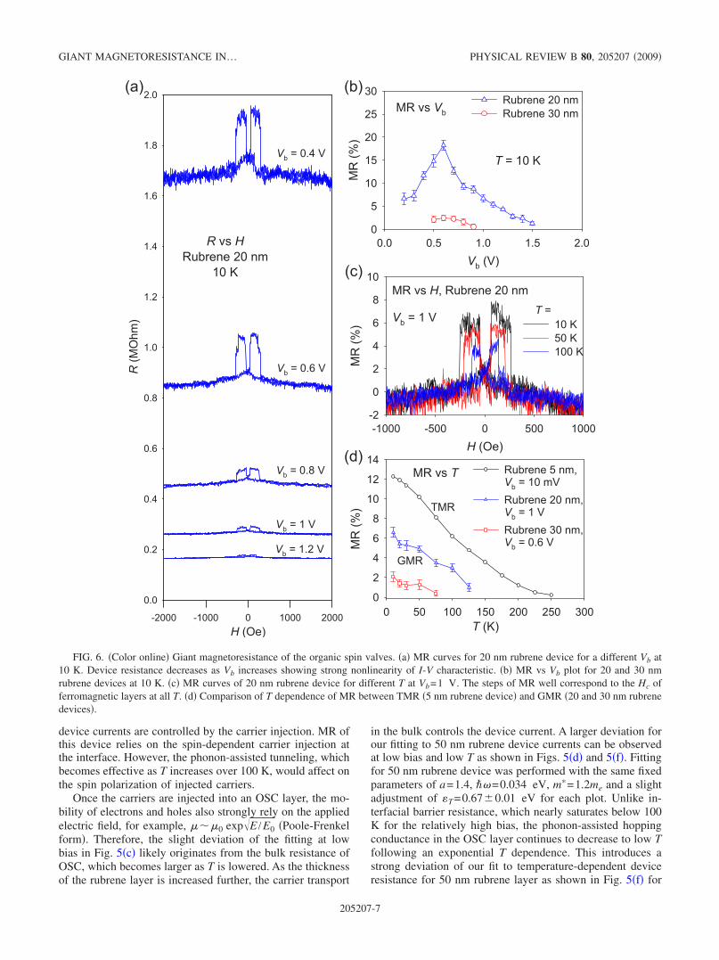
Figure 6�a� displays MR curves for different Vb at 10 Kfor 20 nm rubrene device, which was presented in Fig. 5.Resistance of 20 nm rubrene devices at low-bias and low T isextremely high due to negligible carrier injection, which is incontrast to previously reported low-bias and low-resistanceGMR results at low T for thick layer of OSC spacer.3,6 Forthe 20 nm rubrene device, clear positive MR signals weredetected from 200 mV of Vb. An increase in MR was ob-served up to 600 mV, then MR decreased as Vb increasedfurther �Fig. 6�b��. For the 30 nm rubrene device, MR wasdetectable when the Vb was increased up to 500 mV thenbecame negligible when Vb increased to 1 V �Fig. 6�b��. NoMR was observed for 40 and 50 nm rubrene devices over allT and Vb �up to several V�. We propose the absence of MRfor thick rubrene layers is because the channel distance islonger than the spin-diffusion length ��s� in amorphous ru-brene layer, as viable device current is still measurable aslong as high bias is applied.
MR curves of 20 nm rubrene device for different T atVb=1 V are presented in Fig. 6�c�. The steps of MR curvesat different T well correspond to the Hc of Fe and LSMO aspresented in Fig. 4�d�. This excludes the possibility that themagnetoresistance in our device is induced by ferromagneticFe cluster embedded in OSC layer as proposed by Vinzelberget al.11 The T dependence of MR for 20 and 30 nm rubrenedevices are presented in Fig. 6�d� and compared with T de-pendence of TMR for 5 nm rubene device. No clear MR wasobserved above 150 K for the 20 nm rubrene device. Rapiddrop in MR as T is increased above 100 K for the 20 nmrubrene device can be associated with the thermionic emis-
sion at the interface of the device. For the 30 nm rubrenedevice, the MR disappears above 75 K. The absence of MRfor thicker rubrene devices �d�30 nm� could be attributedto hopping transport and thermionic emission, especially athigh T.
VII. SUMMARY AND CONCLUSIONS
In summary, we presented both TMR and GMR with anOSC spacer and their very different behaviors in response toVb and T. For thick layer of rubrene spacer, the devices arelimited by carrier injection and transport. For the intermedi-ate thickness �d�20 nm�, the carrier injection controls thedevice current. The GMR for intermediate thickness showsstrong Vb and T dependence as a result of the activationprocesses of carrier injection and transport in amorphousOSC layer, in contrast to previous reports3,13 and recent the-oretical study.33 For a thicker OSC layer �d�30 nm�, bulktransport starts to dominate the device current requiringhigher bias for viable device current �space-charge-limitedregime�.
In conclusion, the Vb and T dependencies of our devicesconfirm valid GMR effects via injection and transport ofspin-polarized carriers through the OSC spacer. We ex-plained the carrier injection and transport into/in OSC andtheir impact on the GMR in OSC-based spin valves in termsof phonon-assisted tunneling and hopping in the presence ofstrong electric field. Observation of the spin precession willprovide further proof for the spin transport in the OSC lay-ers, which may require substantial improvement of material’smobility and interfacial quality.
ACKNOWLEDGMENTS
C.B.E. thanks M. S. Rzchowski for helpful discussions.This work was supported in part by the AFOSR under GrantNo. FA9550-06-1-0175, DOE under Grants No. DE-FG02-01ER45931, No. DE-FG02-86ER45271, No. DE-FG02-06ER46327, NSF under Grant No. DMR-0805220, and ONRunder Grant No. N00014-07-1-0215.
1 A. Wolf, D. D. Awschalom, R. A. Buhrman, J. M. Daughton, S.von Molnár, M. L. Roukes, A. Y. Chtchelkanova, and D. M.Treger, Science 294, 1488 �2001�.
2 V. Dediu, M. Murgia, F. C. Matacotta, C. Taliani, and S. Barban-era, Solid State Commun. 122, 181 �2002�.
3 Z. H. Xiong, D. Wu, Z. V. Vardeny, and J. Shi, Nature �London�427, 821 �2004�.
4 P. P. Ruden and D. L. Smith, J. Appl. Phys. 95, 4898 �2004�.5 S. Majumdar, R. Laiho, P. Laukkanen, I. J. Väyrynen, H. S.
Majumdar, and R. Österbacka, Appl. Phys. Lett. 89, 122114�2006�.
6 S. Pramanik, C.-G. Stefanita, S. Patibandla, S. Bandyopadhyay,K. Garre, N. Harth, and M. Cahay, Nat. Nanotechnol. 2, 216�2007�.
7 T. S. Santos, J. S. Lee, P. Migdal, I. C. Lekshmi, B. Satpati, and
J. S. Moodera, Phys. Rev. Lett. 98, 016601 �2007�.8 J. H. Shim, K. V. Raman, Y. J. Park, T. S. Santos, G. X. Miao, B.
Satpati, and J. S. Moodera, Phys. Rev. Lett. 100, 226603 �2008�.9 W. Xu, G. J. Szulczewski, P. LeClair, I. Navarrete, R. Schad, G.
Miao, H. Guo, and A. Gupta, Appl. Phys. Lett. 90, 072506�2007�.
10 J. S. Jiang, J. E. Pearson, and S. D. Bader, Phys. Rev. B 77,035303 �2008�.
11 H. Vinzelberg, J. Schumann, D. Elefant, R. B. Gangineni, J.Tomas, and B. Büchner, J. Appl. Phys. 103, 093720 �2008�.
12 T. Ikegami, I. Kawayama, M. Tonouchi, S. Nakao, Y. Yamashita,and H. Tada, Appl. Phys. Lett. 92, 153304 �2008�.
13 V. Dediu, L. E. Hueso, I. Bergenti, A. Riminucci, F. Borgatti, P.Graziosi, C. Newby, F. Casoli, M. P. De Jong, C. Taliani, and Y.Zhan, Phys. Rev. B 78, 115203 �2008�.
YOO et al. PHYSICAL REVIEW B 80, 205207 �2009�
205207-8
14 A. J. Drew, J. Hoppler, L. Schulz, F. L. Pratt, P. Desai, P.Shakya, T. Kreouzis, W. P. Gillin, A. Suter, N. A. Morley, V. K.Malik, A. Dubroka, K. W. Kim, H. Bouyanfif, F. Bourqui, C.Bernhard, R. Scheuermann, G. J. Nieuwenhuys, T. Prokscha,and E. Morenzoni, Nature Mater. 8, 109 �2009�.
15 M. Cinchetti, K. Heimer, J.-P. Wustenberg, O. Andreyev, M.Bauer, S. Lach, C. Ziegler, Y. Gao, and M. Aeschlimann, NatureMater. 8, 115 �2009�.
16 Y. Q. Zhan, M. P. de Jong, F. H. Li, V. Dediu, M. Fahlman, andW. R. Salaneck, Phys. Rev. B 78, 045208 �2008�.
17 Y. Liu, S. M. Watson, T. Lee, J. M. Gorham, H. E. Katz, J. A.Borchers, H. D. Fairbrother, and D. H. Reich, Phys. Rev. B 79,075312 �2009�.
18 G. Szulczewski, S. Sanvito, and M. Coey, Nature Mater. 8, 693�2009�.
19 M. Johnson and R. H. Silsbee, Phys. Rev. B 35, 4959 �1987�.20 G. Schmidt, D. Ferrand, L. W. Molenkamp, A. T. Filip, and B. J.
van Wees, Phys. Rev. B 62, R4790 �2000�.21 E. I. Rashba, Phys. Rev. B 62, R16267 �2000�.22 H. Yamada, Y. Ogawa, Y. Ishii, H. Sato, M. Kawasaki, H. Akoh,
and Y. Tokura, Science 305, 646 �2004�.23 H. Ishii, K. Sugiyama, E. Ito, and K. Seki, Adv. Mater. �Wein-
heim, Ger.� 11, 605 �1999�.24 J. J. Akerman, R. Escudero, C. Leighton, S. Kim, D. A. Rabson,
Renu Whig Dave, J. M. Slaughter, and Ivan K. Schuller, J.Magn. Magn. Mater. 240, 86 �2002�.
25 J.-H. Park, E. Vescovo, H.-J. Kim, C. Kwon, R. Ramesh, and T.Venkatesan, Phys. Rev. Lett. 81, 1953 �1998�.
26 V. Garcia, M. Bibes, A. Barthélémy, M. Bowen, E. Jacquet, J.-P.Contour, and A. Fert, Phys. Rev. B 69, 052403 �2004�.
27 F. J. Wang, C. G. Yang, Z. V. Vardeny, and X. G. Li, Phys. Rev.B 75, 245324 �2007�.
28 S. Majumdar, H. Huhtinen, H. S. Majumdar, R. Laiho, and R.Österbacka, J. Appl. Phys. 104, 033910 �2008�.
29 T. S. Kim, Phys. Rev. B 72, 024401 �2005�.30 S. Mukhopadhyay and I. Das, Phys. Rev. Lett. 96, 026601
�2006�.31 A. Kiveris, Š. Kudžmauskas, and P. Pipinys, Phys. Status Solidi
A 37, 321 �1976�.32 P. Pipinys and A. Kiveris, J. Phys.: Condens. Matter 17, 4147
�2005�.33 P. A. Bobbert, W. Wagemans, F. W. A. van Oost, B. Koopmans,
and M. Wohlgenannt, Phys. Rev. Lett. 102, 156604 �2009�.
GIANT MAGNETORESISTANCE IN… PHYSICAL REVIEW B 80, 205207 �2009�
205207-9


![#3] Giant Magnetoresistance: Experimentally Driven 1986-1989; Theoretically Modeled 1989; IT Applications into 1990’s First Commerical Hard-Disks with](https://img.pdfslide.us/doc/110x75/56649d925503460f94a79639/3-giant-magnetoresistance-experimentally-driven-1986-1989-theoretically.jpg)