Embed Size (px)
Citation preview

860 IEEE TRANSACTIONS ON COMPUTER-AIDED DESIGN. VOL X. NO 8. AUGUSI I Y X Y
Generation of Performance Constraints for Layout RAVI NAIR, SENIOR MEMBER, IEEE, c . LEONARD BERMAN, MEMBER, I E E E , PETER s. HAUGE, AND
ELLEN J. YOFFA, MEMBER, IEEE
Abstract-In this paper we present methods for generating bounds on interconnection delays in a combinational network having specified timing requirements at its input and output terminals. An automatic placement program which uses wirability as its primary objective could use these delay bounds to generate length or capacitance bounds for interconnection nets as secondary objectives. Thus, unlike previous timing-driven placement algorithms described in the literature, the de- sired performance of the circuit is guaranteed when a wirable place- ment meeting these objectives is found. We also provide fast algo- rithms which maximize the delay range, and hence the margin for error in layout, for various types of timing constraints.
I. INTRODUCTION HE PERFORMANCE of any digital system is limited T by the delay in propagation of signals through the var-
ious paths from the input to the output of the system. In a synchronous sequential circuit, the time taken by the signals to traverse the path between two clocked gates should be no greater than the difference in the times of arrival of successive clock pulses at the two gates. In or- der to simplify analysis, this difference is often approxi- mated as the period of the clock; however, in high-per- formance systems, the difference must account for other factors such as clock skew. In most digital systems, it is convenient, and fairly accurate, to lump the delay asso- ciated with the wire together with the delay associated with the logic components that comprise the system. With such an approximation, the delay of a path through the network may be calculated simply as the sum of the de- lays through the components along that path. In high-per- formance systems, however, in order to accurately esti- mate the delay associated with the wires, it is necessary to know the length, and sometimes the topology, of the interconnection nets driven by the component. This is particularly the case in very large scale integration (VLSI), where the delay associated with the interconnec- tion network may be comparable to the delay due to cir- cuit switching.
Since the length of interconnection nets is not known before actually laying out the components on the chip or board, it is common practice to use an estimate of the interconnection length to compute delays during logic de- sign. After layout, exact lengths are used in order to ver- ify that the system meets performance constraints. If the
Manuscript received September 20, 1988; revised February 17, 1989. The review of this paper was arranged by Associate Editor A. E. Dunlop.
The authors are with the IBM Research Division, Thomas J . Watson Research Center, P.O. Box 218. Yorktown Heights. NY 10598.
IEEE Log Number 8927950.
timing requirements are not met along some paths, an at- tempt must be made to alter the placement and/or the wir- ing to correct them. For example, in [I], correction is attempted by exchanging the locations of components along these paths with other components, or by inserting the components in favorable empty locations. Unfortu- nately, there is no guarantee that a local perturbation to the layout will correct timing errors, especially in high- performance systems where the limits of technology are being pushed by the design. In difficult cases, it is nec- essary to redesign the logic.
Because of the difficulty in altering a completed layout to improve timing, some researchers [ 2 ] , [3] have inves- tigated using timing requirements earlier in the physical design process. Since placement of components is gen- erally done iteratively [4], one approach has been to use progressively more accurate timing information as place- ment proceeds. For example, in [3] timing information is used to evaluate potential placements, and the informa- tion is updated whenever components are perturbed dur- ing the placement process. One problem with this ap- proach is that, in large circuits, it is not unusual to find that interchanging the positions of two components affects over a thousand paths. This could result in long compu- tation times. Another possibility [2] is to pass timing and layout data periodically back and forth between the timing analysis and placement programs while the layout is being constructed.
Two problems arise in both approaches above. First, timing analysis must be done a number of times-some- times a large number of times. Second, since the timing information used during layout is continually changing, the layout may converge rather slowly, or worse, may not converge.
A different approach to the problem uses performance requirements as additional direct constraints during lay- out. Since the length of interconnection, and hence the wirability of the circuit, is optimized by placing compo- nents on an interconnection net as close together as pos- sible, it is possible to identify nets along “critical” paths for special treatment: either earlier consideration during the placement process, or assigning higher weight relative to other nets. For example, in [ 5 ] , it is demonstrated that by using the criticality measure of nets to bias placement and routing programs, the performance of a chip may be brought significantly closer to that of an ideal layout. Similarly, in [6] a hierarchical layout approach is used, with timing computation done at each level of the hier-
0278-O070/89/0800-0860$0 1 .OO 0 1989 IEEE
NAlR e / o/ G k N E R A T I O N OF P E R F O K M A N C E C O N S T R A I N T S 861
archy to determine a criticality class for a net. Each class is associated with a weight which is used to constrain placement at that level of the hierarchy.
The approach outlined in the last paragraph often leads to a layout which meets performance specifications while avoiding the problems mentioned earlier. The principal reason for errors in such an approach is that, in attempting to minimize the length of all nets along a critical path, the problem is often overconstrained to the point where nets which were not critical become excessively long. In this paper, we present a new method for using timing require- ments in the placement process. Our method assigns length bounds to all wires. This relaxes the constraints to be met by the placement program by permitting it to in- crease the wire lengths on noncritical paths while ensur- ing that components on critical paths are close to each other. We introduce the zero-slack algorithm [7], which determines bounds for each net based on timing specifi- cations. Our premise is that while the placement problem is a hard one, it is not more difficult to find a wirable placement which satisfies bounds in length for every net, than one which only minimizes total wire length. In fact, it has been shown in [6] that the imposition of such con- straints on nets does not lead to less wirable solutions. This is possibly due to the fact that, in practice, when a solution exists, there are several placements which satisfy a given wirability constraint.
Since the set of net length bounds that guarantee per- formance requirements is not unique, we also investigate the problem of maximizing the range of permissible lengths for each net. We demonstrate the existence of a fast algorithm for maximizing the range when only upper bounds are important. When both lower and upper bounds are important we formulate the problem as a linear pro- gramming problem, for which polynomial time solutions have recently been demonstrated [8].
11. PRELIMINARIES Our model follows that used in [ 5 ] , [6], and 191. We
assume that, as commonly practised, a given complex se- quential circuit with feedback paths may be broken down into sets of clocked latches having a pure combinational circuit without feedback between the various latch stages. We can thus analyze each group of components forming the combinational circuit between latches independently. As in 161, for simplification, we associate with any com- ponent a single value for delay derived as a function of two delay values, one for a rising transition and one for a falling transition. The procedure to be developed gener- alizes to the case when the values have to be considered separately, as shown in 191. We further assume that all combinations of logic values are possible at the inputs to any component. In practice, we could limit our attention to the subset of values permitted by the logic in order to tighten the timing bounds. However, as shown in [lo], this does not affect the timing results significantly.
In a significant departure from [5] and [6] we consider both late and early modes. In the lute mode, the required
time of arrival of the signal at a specified point is the latest time by which the signal should arrive to ensure proper functioning of the circuit. Conversely, in the eurly mode, the time specified would be the earliest time at which the signal may arrive at that point. (Early mode constraints are needed to accommodate clock skew as well as com- plex clocking strategies common in high performance de- sign.)
For a given combinational circuit coqprised of a set of components X = { x l , x2, . * * , x,,} and a set of inter- connection nets E = { e l , e 2 , * * * , e,ff }, we define a map- Ping
a : X x E -+ ( I , 0, - I }
on every component-net pair as follows:
- 1
1
iff e is an input to x
iff e is an output of x a(x, e ) = r 0 otherwise ( e not connected to x).
Each net e is assumed connected to at least two compo- nents. The r primary inputs to the circuit are treated as the outputs of r dummy components ( I ) in X. We will assume that each component has only one output. In the case where a component has more than one output, we simply replicate the component for the required number of outputs, with identical nets feeding each component. The components providing the q primary outputs of the circuit will be referred to as the output components ( G ). We also assume that “wired outputs” do not exist. These may be handled by introducing additional components at the “wired output” points. Thus we have the relationship n = m + q , since every component other than the output components is associated with exactly one net. Let e ( x ) denote the output net of x.
We now define the set offun-in components of a com- ponent x E X as
r - ( x ) = { x t l r ( x , e(x ’ ) ) = - 1 )
n + ( x > = {x r~a (x ’ , e ( x ) > = - 1 ) .
The mapping a may be represented compactly as the set ofsets, * ( X I = { $ ( x l ) , Ic/(x2), * . 9 1, where
and the set offan-out components as
+ ( X I > = { a+(4 ) U 4). The set ( X ) is often called the net list or the intercon- nection list. The size of the input is characterized by the size of the net list and is given by p , where
P = 1x1 + la+(x)l. Each component x, as mentioned in the last section, is
associated with a delay d ( x ) , which represents the time required for a change in signal at one of its inputs to result in a change at the inputs to components in af (x ) . Thus d ( x ) , besides being a function of the circuitry of com- ponent x, is also a function of the layout characteristics of the net being driven by its output. We define the base
862 IEEE TRANSACTIONS ON COMPUTER-AIDED DESIGN. VOL. 8. NO. 8. AUGUST I 9 X Y
delay, d o ( x ) , as the value of d ( x ) when the components x and R’ ( x ) are located ideally with respect to each other. One could then view the difference,
6 ( x ) = d ( x ) - do(x)
as the contribution to delay due to the net e(x) . Thus, prior to physical design, the sequence of delays Do (X ) = ( d O ( X l ) , dO(X21, . . - , d,(x,,)) are given constants, while the incremental sequence A,( X ) = ( 6,(x1 ), 80(x2), , ?i0(x,)) are unknown because the routes for segments of the net e(x ) are unknown.
For the signal at each output component x E G we are given two type3 of arrival times: the required early time, f r e ( x ) , defined as the earliest time that a signal may arrive at the output of that component, and the required late time, t r p (x ) , defined as the latest time by which it must arrive, for proper processing. In addition, for every primary in- put component x E I , we are given two more arrival times: the actual early time, t,,(x), as the earliest possible time that a change could occur, and the actual late time, t a f ( x ) , as the latest possible time that a change could occur at that primary input.
We could extend the definitions of actual late and actual early times to all components in the circuit. These values, tu, (X ) and tup( X ), may be computed easily, as shown in [9]. Basically, for each x E X such that t,,(z) and t U l ( z ) are specified for all z E a- ( x ) , we set
t , , (x) = d ( x ) + min ta,(z) i E a - (x )
and
t aP(x ) = d ( x ) + max tap(z ) .
An efficient way of implementing this procedure is to per- form a depth--rst search (see [ 1 13) starting at the primary outputs. The complexity of this procedure is O ( p ) , where p is the size of the interconnection list. Thus, for a bounded fan-out circuit, the procedure is linear in the number of circuit components.
For each circuit output, g E G, we can further compute two values, the early slack, s,( g ) , and the late slack, s p ( g ) , as
:ET- (1)
s r ( g > = rac(g) - t r e ( g )
and
s d g ) = t r d g ) - t u d g ) .
Negative values for slack imply that the circuit does not meet the arrival time requirements for the specified values of D ( X ) . In particular, if the base delay values, Do(X) , are used, then the wire contributions, A(X) , are uni- formly 0, and a negative late slack at some output implies that it is impossible for the circuit to meet the perfor- mance requirements. In such cases, the logic needs to be redesigned.
We illustrate the calculations in Fig. 1. For conve- nience, we have shown the calculations for each mode
GI
G2
(b) Fig. 1. Sample calculations of the various arrival times. ( a ) Late mode
calculations. (b) Early mode calculations.
separately. We see that the late slacks are 2 and 0 for outputs GI and G 2 respectively. This implies that some path to G2 is critical in the sense that no further delay can be tolerated along the path. A closer examination reveals that the critical path is the one starting at input I3 and passing through components 2, 4, and 6 to output G ? . If the delay values indicated in the boxes are the base values of delay, this further implies that the layout must ensure that the lengths of nets along this critical path are at their shortest possible values. Any further delay on one of these nets would change the slack on G 2 to a negative value.
In Fig. l(b) we see that the early slacks on both outputs are negative. This means that delay must be added to ap- propriate nets to make the slacks nonnegative. In adding these delays, it is necessary to ensure that the late slacks do not become negative at any output. For example, in- creasing the delays on each of components 5 and 6 by unit value would make the early slacks nonnegative, but would result in a negative slack on G 2 . On the other hand, it is safe to add unit delay to either component 1 or component 3 .
A circuit will be called late-safe if, for every output g E G, sI( g ) 2 0, and early-safe i f s , ( g ) I 0. An assign- ment of incremental delays A (X ) will be termed late-safe if the resulting circuit after adding these delay values re- mains late-safe. A safe circuit is one which is both late- safe and early-safe. Finally, an assignment A ( X ) will be termed safe, if the circuit with delay values D o ( X ) + A (X ) is safe. In the example of Fig. 1 (b), the assignment A ( X ) = { 0, 0, 0, 0, 1, 1 } is not late-safe, while the assignment { 1, 0, 0, 0, 0, 0 ) is safe, because the result- ing circuit is both late-safe and early-safe.
111. ZERO-SLACK ALGORITHM Consider the example in Fig. l(a). We noted that the
addition of any further delay to the critical path would result in an undesirable negative slack at output G ? . On the other hand, a layout for the circuit may add delays to other paths without causing a late path at any output. We present in this section an algorithm that determines a safe assignment A (X ) which is maximal in the sense that any
NAlR er al . : G E N E R A T I O N OF P E R F O R M A N C E C O N S T R A I N T S 863
additional delay on any component x would cause some output to have a negative slack. We call this the zero- slack algorithm. The maximal safe assignment allows us to specify a maximum value on the delay contribution of each net. This in turn may be used to guide the placement of the components. Such a set is not unique. In this sec- tion we demonstrate how one such set may be calculated. The problem of identifying the best set is addressed in Section VI.
First, the definitions for required early time and re- quired late time which were given for the output compo- nents will be extended recursively to all components x E X. If t , , (z) and t r p ( z ) are specified for all z E a+(x), set
rr , (x) = max t r e ( z ) - d ( z ) zea+(x )
and
r rp(x) = min t r p ( z ) - d ( z ) . Z €T+(X)
Again, a depth-first search technique starting at the in- puts provides a procedure to compute these values in 0 ( p ) time, where p is the size of the interconnection list.
In addition, we can compute slack values for every component x E X as before:
sc(x) t a e ( ~ ) - t r e ( x )
and
sdx) = t r p ( x ) - tadx).
Let us define a path as a sequence ( xI, * * ? x k ) , x i E 1 and xk E G, where xi E T + ( x i - I ) for i = 2, * - * , k. We define early and late path slacks, se( p ) and sp( p ) as
s , ( p ) = tat(x1) + d ( x i ) - t r e ( x k ) I < i s k
and
d(x i ) . I < i s k
Essentially, the path slacks reflect the slack at the output component assuming no other paths through the circuit are active.
Lemma I : For any path p = ( xI, x2, * * * , xk ) through the circuit, s p ( x j ) I sp( p ) , 1 I j 5 k.
Proof: By definition,
and
Hence,
leading to
One of the implications of the above lemma is that if the circuit is late-safe, then no output component has a negative late slack and no path has a negative late slack. Another implication is that a circuit remains safe if a de- lay no greater than sp (x ) is added to component x, because such a delay decreases the path slack sc( p ) for any path p through x to sp( p ) - s p ( x ) , which is nonnegative.
Lemma 2: For each component x E X there is some path p, such that s p ( x ) = sp( p,).
, x, = x, * - * , x k ) such that t r p ( x , ) = t ,p (X, + I ) - d ( x , + I ) , for i 1 j , and rap(xI ) = fap(xI - I ) + d ( x , ), for i I j . Such a path must exist by definition of t U p ( x ) and t r r ( x ) . By in- duction,
Proof: Consider the path p, = ( xI, .
f rP(x) = t rp (xk ) - I r J d ( x i + I )
s d x ) = S d P x ) . 0
Lemma 2 implies that if a delay greater than s p ( x ) is added to component x , then there is some path p, for which sp( p,) < 0. This path passes through the output compo- nent xk. By Lemma 1 sp(xk) I sp( p,) , leading us to con- clude that the circuit is no longer late-safe. We also con- cluded from Lemma 1 that it is safe to add a delay no greater than s p ( x ) to component x. Hence we have the following corollary.
Corollary I : Given a safe circuit, an assignment S(x), x E X , is safe iff 6(x) I sp(x). This suggests a procedure to get a maximal set of values for A ( X ) . We could arbitrarily choose a component x having sp(x) < 0, augment the current delay value d ( x ) by 6(x) = s p ( x ) , recompute the slacks, and repeat the process until no components having positive slack re- main.
procedure greedy-zero-slack; {late mode} {Assume original circuit is safe} begin
repeat cornpure-slacks ; S,i" : = 03;
{Find component with positive slack} i : = 1; while i I n and sp(xj) = 0 do i : = i + 1 ;
if i I n then d ( x i ) := d ( x i ) + sp(x;); {Increase delay of i }
until i > n; {all nets have zero slack} end ;

864 IEEE TRANSACTIONS ON COMPUTER-AIDED DESIGN. VOL. 8. NO. 8. AUGUST 1989
The above procedure often leads to situations where the slack on several components along a path become zero even though the delay is lumped with only one component on that path. In contrast to this “greedy” approach, the algorithm shown below distributes delays more uniformly over the components. At each iteration, a component hav- ing the least positive slack is selected. The slack is then distributed as delays over all components whose slacks get reduced to zero.
along path p after assignment A ( x ) be denoted by s; ( p ). Now,
c S(x,) I c S(X,) x j E e n x X l E X
5 min s p ( x , )
I min st(x,).
X , E X
x , ~ n x
procedure zero-slack; {late mode} begin
repeat compute-slacks; S,In : = 03;
{Find minimum positive slack} for i : = 1 to n do
if (sf(x,) < smin) and (sp(xi) > 0) then begin smin : = sp(xi); xmin : = x i ; end ;
if smin # 03 then begin {Find forward path segment}
a0 : = x,,,jn; v : = 0: repeat
find x E a+(a,,) I t rp(x) = trp(a,,) + d(x) and t ,~ (x> = t,p(u,J + d(x); ifxexiststhenbegina,,+l : = x ; v : = U + 1 ; e n d ;
until no such x exists; {Find backward path segment} U := 0; repeat
find x E n-(u,) I t r f (x ) = trp(a,) - d(u) and taP(x) = tUp(a,) - d(u); if x exists then begin a, - : = x ; U : = U - 1 : end ;
until no such x exists;
{Distribute slacks} s := s,,,; for i : = U to U do begin
s := s / ( v - i + 1 ) ; d ( i ) : = d ( i ) + s^; s := s - s^;
(Increase delay of i )
end ;
until smin = m:
While the algorithm is straightforward and easy to im- plement, a proof that it works is a little long. In order to
process of selecting components and the assignment of delay increments to these components leave the circuit safe. Thereafter we show that at each step, all the selected
end ; {all nets have zero slack}
end ;
Hence,
prove that the algorithm works, we will first show that the s ; ( P > = S P ( P ) - ab, ) x,Ee n x
x j E e n x 2 sp(x,) - min s p ( x , ) , by Lemma 1
. , components have their slacks reduced to zero. Finally we show that no component other than the selected ones can have its slack reduced to zero.
Lemma 3: Given a safe circuit, an assignment A ( x ) , x C X , is safe if C,,, 6 ( x i ) I min.r,,x s p ( x i ) .
Proof: Consider any path p through the circuit. Let e denote the set of components in p . Since the circuit is assumed safe originally, sp( p ) 2 0. Let the new slack
2 0, since the circuit is originally safe. The circuit is safe since every path p is safe. 0
Lemma4: L e t p = ( x l ; ~ ~ , x u , ~ ~ ~ , x , , ; ~ ~ , x ~ ) be a path through a circuit such that, for U I i < U ,
t ,p(~;+ I = t r f ( X j ) + d ( x ; + I and f,r,(x;+ I 1 = t,p(x;) + d ( x i + Any assignment of delays to the components ( x u , , x,, ) affects the slack on all the components xu, . . . , x,, equally.

NAIR er U / . : GENERATION OF PERFORMANCE CONSTRAINTS 865
Proof: By choice of U and U , each of the components x u , * - * , x,, must have the same slack. Let pur, represent the path through the circuit that has slack sp( p u , , ) = sp(x,,) - - . . . = sp(x,,). By using the construction in the proof to Lemma 2 such a path may be found as follows: First find p , , , a path which has slack sP(x,,) passing through xu. Then find p , , , a path which has slack sp(x, , ) passing through x,,. Now concatenate the portion up to x,, in p,, with portion between x,, and x,, in p , followed by the por- tion after x,. in p , , .
By Lemma 1 no other path through any of the nodes x,,, * * * , x,. has a smaller slack. Any assignment of delays, 6(x,,), - * * , S(x,, ) , reduces the slack in path pu, , by E,, ,, 6 ( x i ) . Hence, by Lemmas 1 and 2 again, each of the components in x,,, * . . , x,, must have its slack re- duced by E, ,, 6 ( x i ) . 0
Lemma 5: Let p = ( x l r - > X k ), sp( p ) > 0, be a path through a circuit, satisfying the con- ditions, t r p ( X i + l ) = t r l , (x i ) + d ( ~ ~ + ~ ) and t,p(x;+,) = f u p ( x i ) + d ( x i + I ) , for U I i < U . Further, let U and U be extremal values in the sense that at least one of the con- ditions is not satisfied for i = U - 1 and i = U . Let xu, a $ [ U , U ] , be a component in path p such that s F ( x , ) = sp(x, ,) = * * = s p ( x , , ) . For any safe assignment ( 6(x,,), - * , S(x,,) ), the new slack, s; (x,), on component x , must be positive.
Proof: Let a < U . By construction, either tur(xu - , ) < t,r(x,) - d ( ~ ) or t r p ( x u - 1 ) < trp(xU> - d ( x u ) . This implies by definition that either t,p(x,) < t,!(x,) - E,U,,+ I d ( x i ) or trr(x,) < t r p ( x u ) - E,",,, d ( x i ) . In fact, both these inequalities must hold because sp(x,) = sp(x,,). Denote the new required late time at xu as t,!p(x,,), and that at x, as t ;&x,) . By definition,
- , x u , * * , x,,, * *
U
) ( ; = U + I t:r(x,,) = min trp(xa), t:r(xU) - C d ( x ; ) .
Since the incremental delay assignments are made only to those components x i , i > a , the arrival time remains un- changed. Hence tip(x,) = t O r ( x , ) . If t r p ( X , ) I t,!r(x,,) - EY=,+I d ( x ; ) , then = r:r(x,) - Cp(x,) = S A X , ) > 0. Hence the interesting case is when r r l ( x a ) > t:r(x, ,) - d ( x i ) . In this case,
U
> t ,p (x , ) - sp(x,,), as mentioned above
> t r t ( x 0 ) - S P ( ~ , )
' t,P(X,)
> tidx,). Hence the new slack, s ; ( x , ) = f,!p(x,) - tiP(x,,) > 0. A similar line of reasoning for the case when a > U leads to the lemma. 0
7'heorem I : For a given safe circuit, the zero-slack al- gorithm generates an assignment resulting in s p ( x ) = 0 for all x E X , in O ( n p ) time.
Proof: In each iteration of the loop of the zero-slack algorithm, a slack value which is nonzero, and hence pos- itive, is chosen. Delays are distributed along components that have this chosen slack value. Further, the sum of in- cremental delays introduced on these components is ex- actly equal to the slack. By Lemma 3 the circuit remains safe at the end of the iteration. The components on which the slack is assigned satisfy the conditions of Lemma 4. By the same lemma, all chosen components have their slack reduced equally by an amount equal the sum of the incremental delays. Hence the slack on each of these components is reduced to zero. Finally, the procedure en- sures that U and v are extremal in the sense of Lemma 5 . By this lemma, no other component with the same slack value as the chosen components has its slack reduced to zero. All remaining components have either greater slack or zero slack. Components with greater slack cannot have their slack reduced to zero. Components with zero slack are unaffected because by Lemma 3 the circuit is still safe.
At each iteration, the most time consuming operation is the computation of slacks for the circuit. This takes O ( p ) time, where p is the size of the interconnection list. We have proved that at least one component which has non- zero slack gets zero slack at the end of an iteration. By Lemma 1 no component having zero slack can have its slack increased by the introduction of delays. If n is the number of components, then n iterations, taking a total of O ( n p ) time, suffice to make all components have zero slack. 0
The proof of the above theorem suggests the following corollary.
Corollary 2: Every component which has nonzero slack at the beginning is assigned a nonzero incremental delay by the algorithm.
This corollary essentially contrasts the greedy-zero-slack algorithm with the modified zero-slack algorithm. The latter essentially guarantees that if a net is not on an al- ready-critical path, it will be provided with an upper bound on its length which is greater than the minimum possible length for it. In Section VI we will describe an algorithm which assigns a delay of at least c to every com- ponent, where c is the largest value which ensures that the circuit is safe.
We now provide an example to demonstrate how the algorithm works. Fig. 2(a) shows the initial actual arrival time and the required time at each component of the cir- cuit. The path (2, 5 , 8 , 11) is critical. All the components on this path have zero slack. The minimum slack among the rest of the components is 2 and the path ( I , , 1, 4, 7, 10) with x,, = 4 and x,, = 7 satisfies the conditions of Lemma 5 . At the end of this iteration, components 4 and 7 are each assigned an incremental delay of 1 . This re- duces the slack on these components to zero. Continuing
*

866 IEEE TRANSACTlONS ON COMPUTER-AIDED DESIGN. VOL X . NO. 8. AUGUST 1’38’3
G3
(b) Fig. 2 . Demonstration of the zero-slack algorithm. (a) Path segment with
least positive slack at first iteration. (b) Delay assignments for zero slack at end of algorithm.
the process, at the second iteration, component 1 gets as- signed an incremental slack of 2, since its slack is reduced to 2 by addition of delays to components 4 and 7. In three additional iterations, the algorithm assigns incremental delays to the remaining components as shown in Fig. 2(b).
IV. ADAPTATION TO THE EARLY MODE In Section I11 we showed how delays may be assigned
to a late-safe circuit in such a way that the actual late times are exactly equal to the required late times on every path through the circuit. The analogy for the early mode would be an early-safe circuit where negarive incremental delays are assigned to the components such that the actual early times exactly equal the required early times. Such a procedure is uninteresting if the starting point is the set of base delay values, since the resulting delays lead to unimplementable net length values. However, in Section V we will see a situation where the starting delay values on the nets are higher than the base values, and reflect the constraints on net characteristics to be satisfied by the lay- out program. In such situations, the negative incremental delays essentially determine the tolerance to error during layout.
Analogous to the results for the late mode presented in Section 111, we can prove the following:
Lemma 6: For any path p through the circuit, s,(x) 5 se( p ) forx E p .
k , constitute path p. By definition, Proof: Let (xI , * , x = x j , - . . 9 xk), 1 5 j 5
rre(xj ) 2 tr,(xk> - C d(xi) i>j
and
rm(Xj) 5 to,(xl> + ,Z, d(xi). I S J
Hence,
leading to
s&> 5 se( P I . 0
We will just state the remaining results without proofs. As seen above, the proofs are essentially identical to the late-mode case.
Lemma 7: For each component x E X there is some path p x such that s,(x) = se( p, ) .
Let 6,(x) represent the amount by which the delay is reduced at component x. In other words the incremental delay at x is -6,(x).
Corollary 3: Given a safe circuit, an assignment 6 , (x) , x E X , is safe iff 6,(x) 5 s,(x).
Lemma 8: Given a safe circuit, an assignment A,( x), x E X , is safe if
be a path through a circuit such that, for U 5 i < 21,
d(x, + I ). Any assignment of delays to the components xu, 9 x,,
equally.
xk ), s, ( p ) > 0, be a path through a circuit satisfying the conditions r,, (x, + ) = r,, (x,) + d (x, + I ) and r,, (x, + I ) = t,,(x,) + d(x ,+ I ) , for U s i < U. Further, let U and U be extrema1 values in the sense that at least one of the conditions is not satisfied for i = U - 1 and i = U. Let x,, a [ U , U ] , be a component in p such that $,(xu) = s,(x,) = - = se(xl,). For any safe assignment ( 6 ( x u ) , . . , S(x,,) ), the new slack, si(x,), on component x, must be positive.
We could now write a zero-slack algorithm for the early mode in exactly the same way as the algorithm for the late mode, except that the distributed slacks along identified paths are subtracted instead of being added. However, the problem with a procedure implemented as above is that the delays on components at the end of the procedures could be less than their base values, and hence unimple- mentable.
Modijication I: At the end of such a “zero early slack” procedure, set delay values to be max (d(x) , d,(x)) for each x.
This ensures that the circuit is safe and that meaningful values are passed to the placement program. However there could be paths that have positive early slack. More- over, it may have been possible to assign delays in a way that fewer paths have positive slack.
Mod8carion 2: Each time the slack is distributed among components, allocate only as much incremental
6,(x,) 5 minr,,x s,(x,). Lemma 9: Let p = ( x l , * * ,xu, * * , XI,, * * * 9 x!, )
t r e ( x I + ~ ) = rr,(x,) + d ( ~ , + ~ ) a n d r , , ( x , + ~ ) = *,,(x,) +
, x,, affects the slack on all components xu, . . .
Lemma 10: Let p = ( x I , * . . 9 xu, * ’ * , x,,, * 9

NAlR et U / . : GENERATION OF PERFORMANCE CONSTRAINTS 867
delay to a component x such that its resulting delay is at least d , ( x ) .
This ensures that no component gets assigned an unrea- sonable delay. However, we can no longer guarantee that at least one component gets zero slack at each iteration. The algorithm could stagnate with the same set of com- ponents being selected but unmodified at each iteration.
Modijication 3: Perform the algorithm according to Modification 2. If the slack along the identified path in an iteration does not reduce to zero, add the components
procedure near-zero-early-slack; begin
in obtaining a zero-slack safe assignment for the circuit when one exists. An efficient algorithm for obtaining a zero-slack safe assignment is currently not known. We conjecture the existence of an O ( n p ) algorithm for the problem. The distribution of slacks at any iteration is crit- ical in such an algorithm. However, the only practical sit- uation where we are interested in performing a zero-slack algorithm for the early mode is the one to be described in Section V, and in this situation an approximate algorithm, as in Modification 3, suffices. Presented below is Modi- fication 3 as the near-zero-early-slack algorithm.
{early mode)
for i : = 1 to n do Done(x , ) : = false ; repeat
compute-slacks ; s,,, := 00;
{Find minimum positive slack} for i : = 1 to n do
if (not Done@,)) and (s,(x,) < s,,,) and (se(x,) > 0) then begin s,,, : = se(x,); x,,, : = x,; end ;
if smln # 00 then begin {Find forward path segment}
a, := x,,,; 2, := 0; repeat
find x E a+(a,,) I t,,(x) = tre(a,,) + d(x) and fa&) = tue(alJ + 4 x ) ; i f x exists then begin U , , + , := x; ZI := ZI + 1 ; end ;
until no such x exists; {Find backward path segment} U := 0; repeat
find x E a-(a,) 1 t&) = tre(a,) - d(u) and toe@) = tae(uu) - d(u); ifxexiststhenbegina,-, : = x ; u : = u - 1 ; e n d ;
until no such x exists;
{Distribute slacks} s : = s,,,; for i : = U to ZI do begin
s := min ( s / ( v - i + l ) , d(x, ) - do(x,) ); d(x,) : = d(x,) - 2; Done(x,) : = ( d(x, ) - do(x,) = 0 ); s := s - s^;
{Decrease delay ofx,)
end ;
until s,,, = 00;
end ;
end ; The variable Done is a Boolean array variable whose
element is set to true if the delay at the corresponding component has been reduced to its base value. It is easy to see in a manner analogous to Theorem 1 that this al- gorithm takes O ( n p ) time and, further, that it guarantees
along the path to an initially empty Done list. At the be- ginning of each iteration, while identifying the compo- nent with the least positive slack, do not consider com- ponents in the Done list.
We now have a guarantee that some component is re- tired at each iteration. However, the procedure still does not guarantee the generation of a delay assignment in which all paths have zero slack when such an assignment exists. The distribution of slacks at any iteration is critical
that every component having positive initial slack and de- lay greater than the base delay value has its slack reduced in the course of the algorithm.
We noted in Section I11 that if the initial circuit is not late-safe, it is necessary to redesign the logic. On the other

868 IEEE TR ANSACTIONS ON COMPUTER-AIDED DESIGN, VOL. X. NO. 8. AUGUST I989
hand, if the circuit is not early-safe, it can be made early- safe by addition of delays to appropriate components. In the absence of late mode constraints, it is trivial to convert the circuit to a safe circuit and then apply procedure near-zero-early-slack. However in the presence of late- mode constraints, the resulting solution may not be late- safe if the additional delays are not chosen carefully. The problem is further complicated by the fact that there may be no safe assignment, let alone a zero-slack assignment for the circuit in the presence of mixed mode constraints. In Section V we will see a linear programming formula- tion to the problem which can handle this and other cases. The existence of a more efficient solution for these gen- eral cases is, at present, unknown.
V. THE MIXED MODE PROBLEM In this section we will address the problem of simulta-
neously generating upper and lower bounds on the delays. We use the well-studied linear programming approach; several textbooks, e.g. [12], exist on the subject. It is now known [8] that a polynomial time solution exists for the linear programming problem. However, at present, it re- mains unclear whether the new methods are more effec- tive in practice than such older techniques as the Simplex algorithm [13] and its variations, which could take ex- ponential time in pathological cases, but are quite efficient for common examples.
Given a set of required times, t r p ( x ) and t r , (x ) at the output components, x E G, and a set of actual times at the input components, t op (x ) and t o e ( x ) , x E I , we can write the following sets of inequalities from the definitions of required times and actual times:
tur(x) 2 top(z) + d ( x ) ,
f o e ( X ) 5 t,,(Z) + d ( x ) ,
x E x, z E ..-(x)
x € x, z E V ( x )
todx) 5 trp(x>, X E G
tu,(.) I trc(x), X E G
x E x. 4 x 1 2 do(x),
Each line above represents not just one inequality but a set of inequalities. Any feasible solution for the above sets of constraints results in a safe assignment of delay values d ( x ) , for x E X . Such a solution is safe, even if the circuit with base delay values is not early-safe. Fur- ther, the last set of constraints ensures that if a solution exists then the delays must be greater than the base delay values, and hence implementable. (Because of this re- striction, the initial circuit must be late-safe. No feasible solution can exist if it is not.) Finding a feasible solution or determining that none exists may be done in polyno- mial time by the ellipsoid algorithm [8]. A more practical approach may be to treat the constraints as those of a lin- ear programming problem with a null objective function. Any feasible solution would then serve as an optimal so- lution to the resulting instance of the linear programming problem.
Solving the linear programming problem to obtain a feasible solution provides only one set of delay values for safe operation of the circuit. This set could be used to generate net length constraints for placement. Unfortu- nately, it would be impossible in practice to generate a placement in which every net has a specified length. It is more useful to generate a range of delay values for each component, such that any net lengths that correspond to delays within this range guarantee safe operation of the circuit. Further, in order to maximize the tolerance to er- ror in placement, we wish to generate these delay bounds in such a way that the minimum difference between these bounds, calculated over all nets, is maximized.
We define a minimum set of safe delay values { d, ( x ) } as one in which, for each x , d , ( x ) 1 d o ( x ) and reducing d, ( x ) causes the circuit to be no longer safe. Similarly, a maximum set { d2 ( x ) } is defined as one in which, for each x , d2(x) 2 d o ( x ) and increasing d 2 ( x ) causes the circuit to be no longer safe. We note that for a given component x , it may be possible to either reduce d , ( x ) or increase d 2 ( x ) in conjunction with changes in delays on other components. Hence there are several possible minimum and maximum sets. We observe here that the zero-slack algorithm generates a maximum set in the presence of late- mode constraints alone, while the near_zero_early_slack algorithm determines a minimum set in the presence of early-mode constraints alone.
Let us define a compatible set of delay values as a set of delay pairs { ( d , (x ) , d 2 ( x ) ) } , where { d , ( x ) } is a minimum set and { d2 ( x ) } is a maximum set, and for each x , d 2 ( x ) > d, ( x ) . Given a compatible set we may trans- late the delay values on each component to length bounds on their respective output pin nets. We are guaranteed that if these delay ranges are satisfied by a placement then the circuit is safe, i.e., the early and late timing constraints are satisfied. Let us define the range of a compatible set to be minAGx ( d 2 ( x ) - d, (x ) ) . Shown below is a linear programming formulation, a solution to which determines the maximum possible range of any compatible set for a given set of timing constraints.
Maximize c, subject to the constraints:
tap(x) 1 tup(z) + d ( x ) + c ,
to,(.) 5 tUF(Z) + d ( x ) ,
x E x, z E c ( x )
x E X , z E Y ( x )
t o ~ ( x ) 5 trp(X), X E G
tu,(.) I tre(x), X E G
d ( x ) 2 do(x), X E X
c I 0.
A solution to the above, if one exists, determines safe values d ( x ) for each x in such a way that d ( x ) + i; is also safe, where C is the optimal value of c. There can be no other set of safe delay values for which c > F. Typically these values will reduce the slack only on a few of the components to zero. Thus the layout will be overcon-
NAlR ct ul.: GENERATION OF PERFORMANCE CONSTRAINTS -- ._
869
strained if every net is specified an upper bound on its delay contribution that is only C units greater than its lower bound. In order to give a greater degree of freedom to other less critical nets, we apply the zero-slack procedure as described below, starting with the sets { d ( x ) } and { d ( x ) + C } just found.
Step 1) Solve the linear programming problem as men- tioned above. Let C be the maximum range de- termined. Let d ( x ) be the values of d ( x ) in the solution.
Step 2) With initial delays of d ( x ) + C on each com- ponent, perform the zero slack algorithm for the late mode. Let { d 2 ( x ) } represent the re- sulting maximum set.
Step 3) With initial delays of d ( x ) on each component, perform the near-zero-early-slack algorithm for the early mode. Let { d , ( x ) } represent the resulting minimum set.
The resulting values represent a compatible set with optimum range. For any other compatible set { (d;(x), d i ( x ) ) } , it must be the case that minall, ( d i ( x ) - d ; ( x ) ) I C.
The above procedure may be modified to obtain better delay ranges for noncritical nets. Notice that if there is a path through the circuit which is already critical in both the early and late modes, C will be zero. Even when this is not the case C is likely to be very small, determined by the near criticality of paths involving a rather small frac- tion of components. In such a case, it would be beneficial to run through the linear programming phase again, freez- ing the minimum and maximum delays on the components which have zero slack at the end of the first run of the linear programming problem. This procedure could be re- peated until the linear programming formulation at some point has no feasible solution. Such an iterative procedure maximizes the assignment on at least one component at each iteration; however, it takes too long to run-in the worst case, as many n instances of the linear program- ming problem may have to be solved. To speed up the solution, at the end of each iteration one could retire from consideration components having small slack, in addition to components having zero slack.
Let us now return to the late-mode problem. In many cases, the initial circuit is already early-safe. In such cases, d l (x) is going to be uniformly zero, and early mode calculations are not needed. In the next section we pro- vide a fast algorithm for finding the optimum range in such situations.
VI. OPTIMAL ASSIGNMENT FOR LATE MODE Let us reconsider the late mode zero-slack algorithm.
In Section I11 we provided an algorithm that guarantees that all components have zero slack when such an assign- ment exists. The algorithm heuristically partitioned the slacks as delays among the nodes. On the other hand, in Section V we saw a linear programming formulation for the more general problem which guarantees an optimal
range for the delays assigned to the components. As men- tioned at the end of the section, we could remove some of the constraints to obtain an optimal solution when early mode constraints are absent. Such a formulation is shown below:
Maximize c, subject to the constraints:
t,y(x) 2 tu&) + d,(x) + c, x E x, z E .-(x)
tadx) I t r r ( 4 ~ E G
c 2 0. Clearly, c is maximized when d ( x ) = d,(x); hence the
absence of variables { d ( x ) } . Having obtained the opti- mal value C it suffices to run the zero-slack algorithm as in Section I11 using d,(x) + C as the starting value for each x . The asymptotic complexity of such a procedure depends on the complexity of the procedure to solve the linear programming problem. Fortunately the above prob- lem is structured in a way that allows an alternative effi- cient algorithm for its solution. In the rest of this section we will demonstrate such an algorithm.
Let R represent the nonnegative real number system. We define a Efunction as a mapping E : R -+ R satisfying the following properties:
1) It is convex, i.e., X ( ( 1 - X ) p + Xq)
2) It is piecewise linear. 3) Each of the linear regions has a positive, integer
5 ( 1 - X)E(p) + XE(q), 0 < X < 1.
slope.
An example of a E function is shown in Fig. 3 . We can identify a E function using the minimum set of
lines of which it is the envelope. Thus the ordered set of
characterizes such a function completely, with the com- ponent lines defined by equations T = f( r ) = m,r + b, , 1 5 i I n. We will call b, the offset of the line with slope m,. For example, the E function of Fig. 3 is characterized by { (1 , 6), (2 , 4), ( 3 , 0)} as shown in Fig. 4. We will define the steepness, E, of a E function as its highest slope, m,. Let X I , E 2 , and E3 represent three E functions with steepness E l , E 2 , and t 3 , respectively. The following properties, somewhat analagous to those of convex func- tions, follow from the definitions above:
Lemma 11: The sum, X I + E 2 , of two X functions, E l and E 2 , is a E function with steepness t1 + t2 .
Lemma 12: The maximum, max (E,, E 2 ) , of two E functions, E , and E 2 , is a E function with steepness max
Lemma 13: max ( X i , E 2 , X7) = max (max ( E I , X 2 ) , X 3 ) with steepness max ( t l , t 2 , t3 ) .
Lemma 13 provides a bound on the steepness and hence the number of component lines for the maximum of a set of E functions. We give below an efficient procedure to compute this maximum 5 function. Assume that there are k X functions, the ith function E , being characterized by
pairs {(mi, h ) , (m2, b2), . 7 (m,,, h7)I3 m, < m,+19
( 4 1 9 ‘ $ 2 ) .

870 IEEE TRANSACTIONS ON COMPUTER-AIDED DESIGN. VOL. 8. NO. 8. AUGUST 1989
At the end of the procedure, the set { ( m i , bi), (m;, b;) , . * , (m;,, b;.)} characterizes the maximum. The procedure works as follows: In line Ll , the steepness of the maximum, and thereby the set of possible slopes, is determined. In L2 the procedure eliminates lines for which there are other lines with the same slope and a larger offset. Beginning at L3, the procedure generates the com- ponents of the maximum. It does this by iteratively gen- erating the envelope of components up to a slope j from the envelope of components with slopes less than j . Spe- cifically, in L4, the procedure eliminates those compo- nents of the current envelope which do not form part of the next envelope. At any iteration, s represents the num- ber of components in the current envelope and U, repre- sents the abscissa ( 7 coordinate) of the point at which the line with slope j intersects the envelope of lines with slopes less than j . For two consecutive slopes j and k in the envelope, j < k, it must be the case that a, < ak.
For example, consider the set { ( 1 , 6), (2, 4) , (3, 0) , (5, 2 ) ) . The quantity a l is set to -6. The intersection of line (1, 6 ) with ( 2 , 4) leads to az = 2. Hence the enve- lope of lines with slope 2 or less is { ( 1, 6) , ( 2 , 4 ) }. For slope 3, we have a3 = 4. Since a3 > u2 , no component of the current envelope is discarded. The line (5, 2 ) in- tersects line (3, , 0) at x = 1. So line ( 3 , 0) cannot be a component of the next envelope because a3 = 4. Simi- larly the intersection of ( 5 , 2) with (2, 4 ) occurs at 7 = 2 / 3 . Since a2 = 2, we discard the line (2, 4 ) also. Fi-
Fig 3. Sample Z function.
T = 3 r
T = 2 r + 4
T = 7 + 6
Fig. 4. Z function of Fig. 3 characterized by { (1 , 6 ) . ( 2 , 4), ( 3 , 0 ) )
nally, ( 5 , 2) is intersected with ( 1, 6). This results in u5
- procedure muxE (EI , E 2 , begin {Compute steepness of maximum }
L1. f o r i : = 1 t o k d o t := max(t,m,, , ,) ;
* , ck);
t := 0;
{Compute maximum offset for each slope} forj := 1 to 4 do bmux, := -03;
L2. fori := 1 tokdo forj := 1 ton, do b-,,,,., : = max (b-,,,,,, , b,,j 1;
s := 0; a. := -CO; ml, := 0; bh := 0; L3. forj := 1 to 4 do
ifb, # -03 then {line segment with slope j exists} begin
s := s + 1; mi := j ; b; := bmax,; {intersect with line of lower slope}
C,’-I - c,’ . m: - m.v - 1
I ’ a, :=
L4. while (a, < a, - do {Continue intersecting until a, > a, - I }
s := s - 1; mi := m i + l ; bi := b i + l ; begin
Ci-1 - c,’ . a, :=
mi - m l P l ’ end ;
end ; n’ := s; {Number of line components in the maximum} end ;

NAIR cf U/.: GENERATION OF PERFORMANCE CONSTRAINTS 87 I
= 1, which is greater than a l . Thus there are two surviv- ing lines { ( 1, 6 ) , ( 5 , 2 ) ) forming the final envelope.
Lemma 14: Procedure max E determines the maximum of k Z functions each with steepness 5 ,$ in O ( k ( ) time.
Proof: The initial operation of uniquely identifying one line for each slope takes O ( k , $ ) time as implemented above. We now need to bound the number of times a line intersection is calculated. Observe that whenever an in- tersection is made for a selected slope, either the line that it is intersected with is discarded, or the intersection is retained. In the latter case, the next higher slope is se- lected. Since each slope is selected once, at most ( inter- sections are retained. Since a line once discarded is never intersected with any other line, at most ,$ intersections re- sult in discarded lines. Thus at most 2,$ intersections are
Let us now consider a circuit C with specified actual late arrival times tap( 1 ) at the inputs and required late ar- rival times trr( G ) at the outputs. The basic delays for the components is { d o ( x ) }, x E X . Assume that a variable delay 7 is added to every component, resulting in the de- lay set { do(x) + .}. If the circuit is originally safe, then as 7 is increased from 0, a value ? is reached beyond which the circuit is never safe. Let t a r (x , 7) represent the actual arrival time at component x as a function of 7 .
Lemma 15: For any component x E X , if t u p ( z , 7), z E n- ( x ) are E functions with respect to r with steepness t z , then tup (x , 7) is also a X function with respect to 7. Fur- ther, the steepness of t a r (x , 7) is l + max,,,-(,) (:.
Proof: By definition, tup (x , 7) = max,,,-(,) tup(z, 7) + d(x ) . By Lemma 13, maxz,,-(,) tur (z , 7) is a E func- tion with steepness maxzer-(,) 4,. Now d ( x ) = d o ( x ) + 7, and is hence a E function with steepness 1. Hence by Lemma 1 1 we have the desired result.
0
A simple procedure to compute the actual late time as a function of 7 for every component is shown below. We assume that two n-dimensional arrays { m,} and { b, } contain the information characterizing the n E functions.
calculated by the procedure. 0
procedure compute- function ( x , X , ) ; begin
for z E F ( x ) do
c, : = max X ( X , 1 z E n- (x ) ) ; visited(x) : = true ;
if not visited(z) then compute-function(z, E:); c(
end ; Define the depth of a component x in a circuit as fol-
lows:
i f x E I depth ( x ) = [:’+ zy;, deprh(x), otherwise.
The depth of a component also indicates the maximum number of components that are in any path from the pri- mary inputs to that component. Define the depth of a cir- cuit as the maximum depth of any component in the cir- cuit. Computing the depth of a circuit is essentially a topological sorting of the components, an operation which can be done in a depth-first manner in O ( p ) time, where p , as usual, is the size of the interconnection list. Since the primary input components x E I have given constant values for t U p ( x ) , we can prove the following by induc- tion:
Lemma 16: For a component x E X in a circuit, tUp(x, r ) , expressed as a function of a uniform delay parameter 7, is a E function with steepness equal to the depth of the component.
The maximum value of 7 for which the circuit is still safe is given by
? = min 7, I tal( U , 7 = T ~ , ) = trt( U ) .
It is easy to see that any 7 > ? will violate the late timing requirement at some primary output.
The code below illustrates the computation of the op- timum value for r . We assume that when t a p ( x ) is com- puted for each x in procedure compute-function, the dis- continuity points of the corresponding E function are also saved in the vector {a,,,}, 1 I i I k , , where k, is the number of component line segments in t u p ( x ) .
W €G
function ?(G: output-component-set): real; begin
for x E X do visited(x) : = false ; ? : = 00; {Initialization} for w E G do begin
compute-function(w , E , ) ; {Solve for 7,) for i : = 1 to k , do begin {Check intersection with ith segment}
if 7, < + , then leave ; {Intersection found} end ; i f ? > r , then ? := 7,;
end end ;
872 IEEE TRANSACTIONS ON COMPUTER-AIDED DESIGN, VOL.. 8. NO. X. AUGIJSI‘ 19x0
Lemma 17: Computation of { r,,,,( G, 7) } at the outputs to a circuit E as a function of a uniform delay parameter 7 takes O ( p depth( C ) ) time, where p is the size of interconnection list.
Proof: To compute the values of t,?( G, 7) we suc- cessively compute the r[ , ,(x, 7 ) functions for the compo- nents starting at the primary inputs, in increasing depth order. This is essentially a depth-first traversal starting at the outputs and is implemented recursively as shown in the procedure above. From Lemmas 14 and 16 we note that the computation of t,,,(x, 7) for any x takes O ( f a n i n ( x ) dep th (x ) ) time, where fan in(x ) = I n- ( x ) 1 . Since depth ( x ) is bounded by depth ( C ), and since the size of the interconnection list, p , is simply E.,
0
Theorem 2: Computing the optimum value of 7 takes O ( p * depth ( C ) ) time, where p is the size of the inter- connection list for circuit.
Proof: We refer to the function ? above, which com- putes the optimum value for 7. By Lemma 17 the total computation involved with the compute-function proce- dure is O ( p . depth ( C ) ) . As implemented, solving for 7, takes O ( ( , ) time. In any case, the total computation of this part is bounded by 0 ( q depth ( C )), where q =
0
As in Section V the zero-slack algorithm may now be invoked, assuming that the delay on each component x is d o ( x ) + ?. The resulting incremental delay values when added to ? give zero-slack delay assignments for the orig- inal circuit: any value of 7 greater than ?, when uniformly assigned to all components in the circuit would violate the late timing requirements at at least one of the primary out- puts.
As mentioned at the end of Section V, it may be the case that ? as determined by the above procedure is zero or very small. In these cases, not much is gained by com- puting the value of ? by the above procedure. However, as mentioned there, it would still be possible to optimize the incremental delay assignments on the remaining com- ponents by freezing the delay assignments on the com- ponents with zero or small slack. The top( U ) values at the outputs remain E functions, possibly with lower steep- ness, because “frozen” delays are themselves ,” func- tions with steepness 0. The resulting value of ? provides the additional delay that may be safely added to the re- maining components. This process may then be continued or the zero-slack algorithm invoked to get upper bounds on delays for the remaining components.
( 1 + fanin (x ) ) , we have the required result.
I G 1 . Since q < p , we have the desired result.
VII. CONCLUDING REMARKS
We have presented a new approach to the problem of physical layout of circuits with specific performance con- straints. The idea behind the approach has been embodied in an efficient algorithm called the zero-slack algorithm. In contrast to previous approaches, our technique guar- antees that satisfying the constraints on each net individ-
ually satisfies the performance requirements on the circuit as a whole. The zero-slack algorithm has been imple- mented and is being used in the design of circuits within IBM.
The approach has been exercised on a number of CMOS parts, ranging from a macro with 291 components (358 nets) to a 9 mm semicustom chip having over 5000 com- ponents ( > 8000 nets). We performed a series of exper- iments on one of the parts to demonstrate the effectiveness of the approach. This circuit involved 1325 components and 1599 nets. The timing analysis and zero-slack algo- rithm were done within a logic synthesis system environ- ment (LSS [ 141). The zero-slack algorithm generated de- lay increments for each component, which were then transformed to upper bounds on net capacitances using delay equations for the cell library. The CPU time needed to read the design into the LSS data base, run timing anal- ysis, and perform the zero-slack algorithm was 9 min on an IBM 3090. Of this, the time taken to calculate the max- imum delays for nets and convert these delays to maxi- mum capacitance values was 200 s. The placement algo- rithm used was a simulated annealing [I51 program, widely used within the company. The program could be set up to optimize weighted functions of several parame- ters, one of which was the maximum permitted capaci- tance of each net.
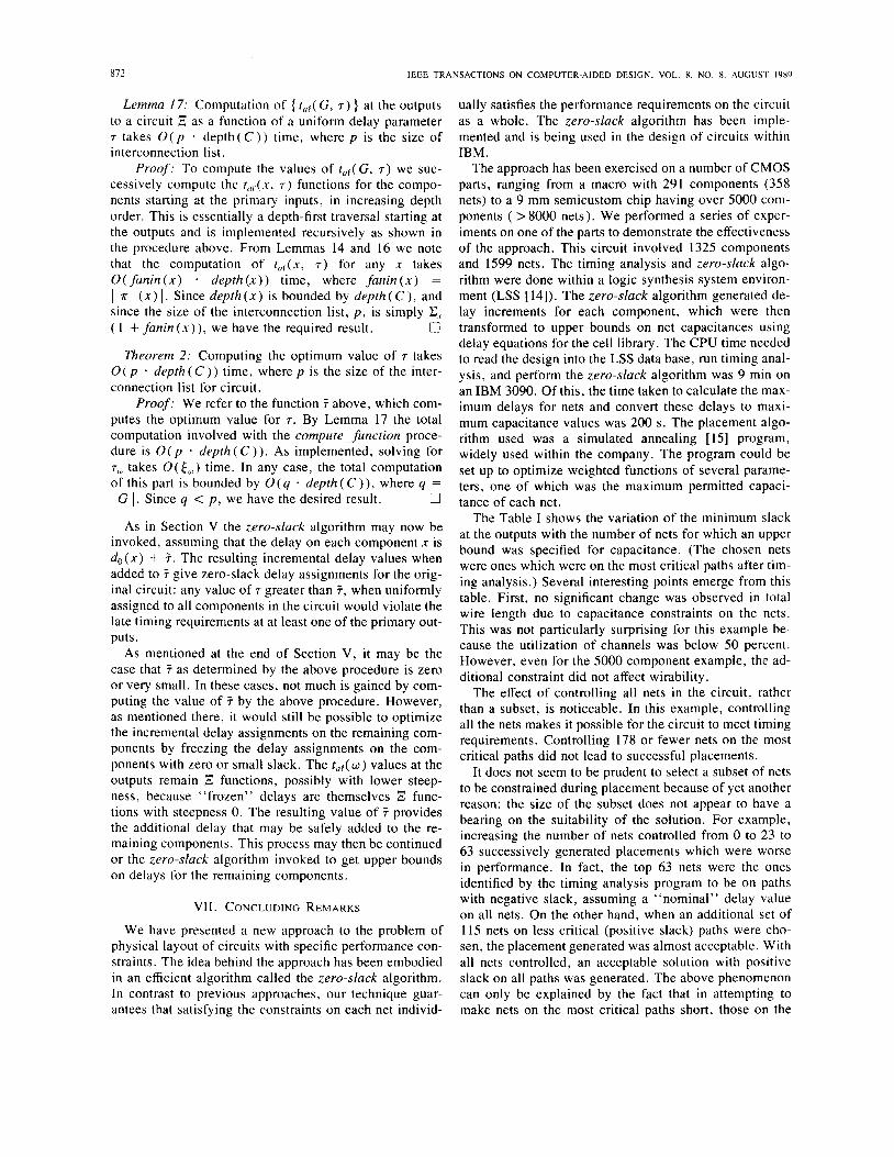
The Table I shows the variation of the minimum slack at the outputs with the number of nets for which an upper bound was specified for capacitance. (The chosen nets were ones which were on the most critical paths after tim- ing analysis.) Several interesting points emerge from this table. First, no significant change was observed in total wire length due to capacitance constraints on the nets. This was not particularly surprising for this example be- cause the utilization of channels was below 50 percent. However, even for the 5000 component example, the ad- ditional constraint did not affect wirability .
The effect of controlling all nets in the circuit, rather than a subset, is noticeable. In this example, controlling all the nets makes it possible for the circuit to meet timing requirements. Controlling 178 or fewer nets on the most critical paths did not lead to successful placements.
It does not seem to be prudent to select a subset of nets to be constrained during placement because of yet another reason: the size of the subset does not appear to have a bearing on the suitability of the solution. For example, increasing the number of nets controlled from 0 to 23 to 63 successively generated placements which were worse in performance. In fact, the top 63 nets were the ones identified by the timing analysis program to be on paths with negative slack, assuming a “nominal” delay value on all nets. On the other hand, when an additional set of 115 nets on less critical (positive slack) paths were cho- sen, the placement generated was almost acceptable. With all nets controlled, an acceptable solution with positive slack on all paths was generated. The above phenomenon can only be explained by the fact that in attempting to make nets on the most critical paths short, those on the
NAlR C / U / . : GENERATION OF PERFORMANCE CONSTRAINTS
# nets controlled 1570
Worst slack (ns.) 0.543
Total lennth (wire units) 476
873
178 63 23 0 Ideal’
-0.355 -4.024 -3.510 -0.953 5.506
467 462 457 451 0
* Ideal implies zero delay on interconnections
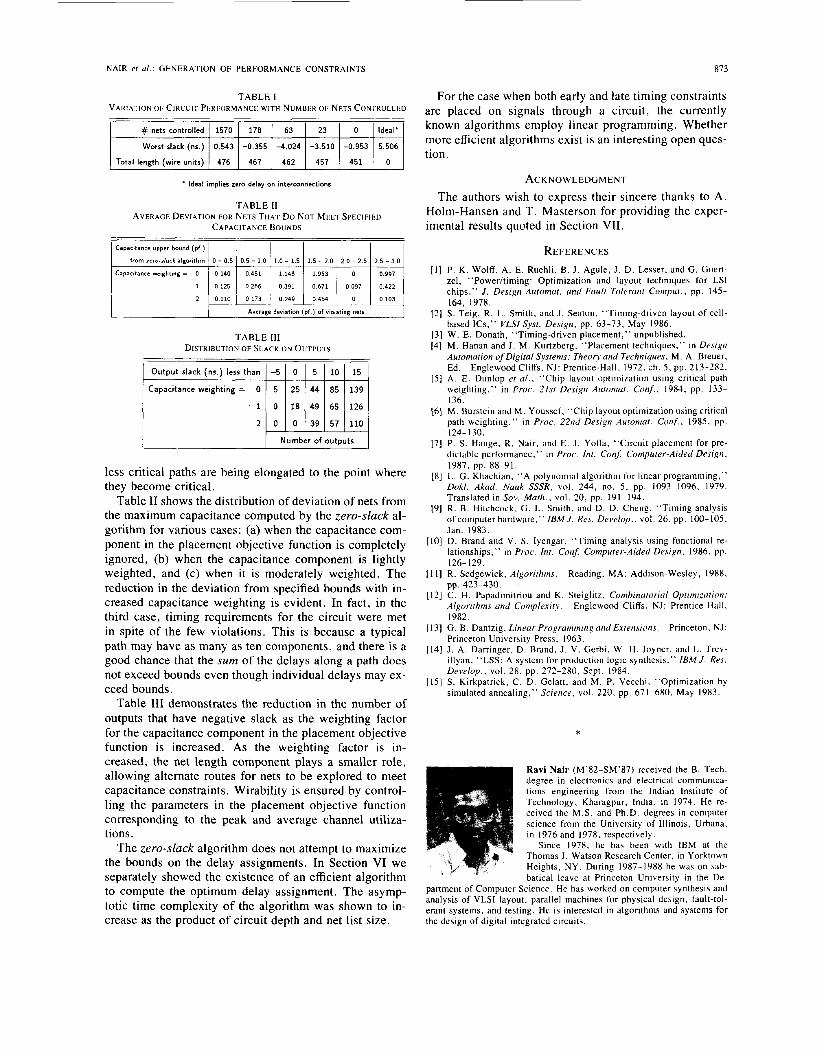
TABLE I1 AVERAGE DEVIATION FOR NETS THAT DO NOT MEET SPECIFIED
CAPACITANCE BOUNDS
Capacitance upper bound (pf.)
TABLE I11 DISTRIBUTION OF SLACK ON OUTPUTS
N u m b e r of outouts
less critical paths are being elongated to the point where they become critical.
Table I1 shows the distribution of deviation of nets from the maximum capacitance computed by the zero-slack al- gorithm for various cases: (a) when the capacitance com- ponent in the placement objective function is completely ignored, (b) when the capacitance component is lightly weighted, and (c) when it is moderately weighted. The reduction in the deviation from specified bounds with in- creased capacitance weighting is evident. In fact, in the third case, timing requirements for the circuit were met in spite of the few violations. This is because a typical path may have as many as ten components, and there is a good chance that the sum of the delays along a path does not exceed bounds even though individual delays may ex- ceed bounds.
Table 111 demonstrates the reduction in the number of outputs that have negative slack as the weighting factor for the capacitance component in the placement objective function is increased. As the weighting factor is in- creased, the net length component plays a smaller role, allowing alternate routes for nets to be explored to meet capacitance constraints. Wirability is ensured by control- ling the parameters in the placement objective function corresponding to the peak and average channel utiliza- tions.
The zero-slack algorithm does not attempt to maximize the bounds on the delay assignments. In Section VI we separately showed the existence of an efficient algorithm to compute the optimum delay assignment. The asymp- totic time complexity of the algorithm was shown to in- crease as the product of circuit depth and net list size.
For the case when both early and late timing constraints are placed on signals through a circuit, the currently known algorithms employ linear programming. Whether more efficient algorithms exist is an interesting open ques- tion.
ACKNOWLEDGMENT The authors wish to express their sincere thanks to A .
Holm-Hansen and T. Masterson for providing the exper- imental results quoted in Section VII.
REFERENCES [ I ] P. K. Wolff. A. E. Ruehli, B. J . Agule. J . D. Lesser. and G . Goert-
zel, “Power/timing: Optimization and layout techniques for LSI chips.” J . Design Automat. and ~ ~ ~ u / t - T o / e r c l n r Coinput.. pp. 145- 164, 1978.
[2] S . Teig, R. L. Smith, and J . Seaton. “Timing-driven layout of cell- based ICs,” VLSI Syst. Design, pp. 63-73, May 1986.
131 W. E. Donath, “Timing-driven placement,” unpublished. [4] M. Hanan and J . M. Kurtzberg, “Placement techniques,” in DesiRn
Automation of Digital Systems: Theory and Techniques, M . A. Breuer, Ed. Englewood Cliffs, NJ: Prentice-Hall, 1972, ch. 5 . pp. 213-282.
[ 5 ] A. E. Dunlop et a l . , “Chip layout optimization using critical path weighting,” in Proc. 21st Design Automat. Conf.., 1984, pp. 133- 136.
[6] M. Burstein and M. Youssef, “Chip layout optimization using critical path weighting,” in Proc. 22nd Design Automat. Conf.. 1985. pp. 124-130.
171 P. S . Hauge, R. Nair, and E. J . Yoffa. “Circuit placement for pre- dictable performance.” in Proc. Int. Conf: Computer-Aided Design.
[8] L. G. Khachian, “A polynomial algorithm for linear programming.” Dokl. Akad. Nauk SSSR, vol. 244, no. 5 , pp. 1093-1096, 1979. Translated in Sov. Math., vol. 20, pp. 191-194.
[9] R. B . Hitchcock. G. L. Smith, and D. D. Cheng, “Timing analysis ofcomputer hardware,” IBMJ. Res. Develop., vol. 26, pp. 100-105. Jan. 1983.
IO] D. Brand and V. S . Iyengar, “Timing analysis using functional re- lationships.” in Proc. Int. Con$ Computer-Aided Design, 1986. pp. 126- 129.
1 I] R. Sedgewick, Algorithms. Reading, MA: Addison-Wesley, 1988,
121 C. H. Papadimitriou and K. Steiglitz, Combinatorial Optimization: Algorithms and Comp1exit.v. Englewood Cliffs. NJ: Prentice-Hall, 1982.
[I31 G. B. Dantzig, Linear Programming and Extensions. Princeton, NJ: Princeton University Press, 1963.
[I41 J . A. Darringer, D. Brand, J . V. Gerbi, W. H . Joyner, and L. Trev- illyan, “LSS: A system for production logic synthesis.” IEM J . Res. Develop.. vol. 28, pp. 272-280, Sept. 1984.
1151 S. Kirkpatrick, C. D. Gelatt, and M. P. Vecchi. “Optimization by simulated annealing,” Science. vol. 220. pp. 671-680, May 1983.
1987, pp. 88-91.
pp. 423-430.
*
Ravi Nair (M’82-SM’87) received the B . Tech. degree in electronics and electrical communica- tions engineering from the Indian Institute of Technology, Kharagpur, India, in 1974. He re- ceived the M.S. and Ph.D. degrees in computer science from the University of Illinois, Urbana, in 1976 and 1978, respectively.
Since 1978, he has been with IBM at the Thomas J . Watson Research Center, in Yorktown Heights, NY. During 1987-1988 he was on sab- batical leave at Princeton University in the De-
partment of Computer Science. He has worked on computer synthesis and analysis of VLSI layout, parallel machines for physical design, fault-tol- erant systems, and testing. He is interested in algorithms and systems for the design of digital integrated circuits.
874 IEEE TRANSACTIONS ON COMPUTER-AIDED DESIGN, VOL. 8. NO. x. AUGUST 19x9
is automatic logic des
C. Leonard Berman (M'88) was born in Jersey City, NJ, in October 1949. He received the B.S. degree in mathematics (with honors) from the California Institute of Technology, Pasadena, CA. in 1971. the M.A. degree in mathematics from Cornell University, Ithaca, NY, in 1973, and the Ph.D. degree in computer science in 1977.
He has been at IBM Research since then, ex- cept for 1984-1985, when he held a visiting ap- pointment at the Massachusetts Institute of Tech- nology, Cambridge, MA. His main research area
ign.
* Peter S. Hauge received the B.S., M.S., and Ph.D. degrees in electrical engineering in 1961, 1963, and 1967, respectively, from the University of Minnesota, Minneapolis.
He is manager of a group concerned with per- formance-driven VLSI physical design at the Thomas J . Watson Research Center, where has been since he joined IBM in 1968. He has devel- oped physical design systems for cascode voltage switch macros and chips, and is currently explor- ing fast, timing-related heuristics for physical de-
sign automation tools. Until 1980. when he joined the Computer Science Department, he studied the interaction of microwave, infrared and visible radiation, with semiconducting materials and films. He is the coinventor of two automated instruments for on-line semiconductor process control.
Dr. Hauge is a member of the Optical Society of America.
* Ellen J. Yoffa (M'86) received the B.S. and Ph.D. degrees in physics from the Massachusetts Institute of Technology, where her area of study was theoretical solid-state physics.
In 1978, she joined the IBM Thomas J . Watson Research Center for postdoctoral work in the Semiconductor Science and Technology Depan- ment, where she investigated ballistic conduction in semiconductor devices and the physics of the laser annealing process. Since 1980, she has been a member of the research staff in the Computer
Science Department and is currently senior manager of the System Design and Verification Department, where she is responsible for managing re- search in tools for computer-aided design of VLSI chips, including system description and early design tools, logic synthesis, and hardware and soft- ware logic simulation. She is a member of the editorial board of l E E E Design and Tesf of Computers. Her research has involved the development of tools for VLSI physical design automation.
Dr. Yoffa is a member of Phi Beta Kappa and Sigma Xi.