Embed Size (px)
Citation preview
PT4115E
50V/1.5A Step-down High Brightness LED Driver
CR POWTECH (SHANGHAI) CO., LTD. WWW.CRPOWTECH.COM Page 1 PT4115E_DS_Rev EN 1.0
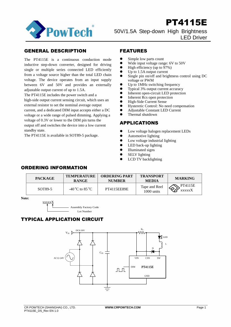
GENERAL DESCRIPTION
The PT4115E is a continuous conduction mode
inductive step-down converter, designed for driving
single or multiple series connected LED efficiently
from a voltage source higher than the total LED chain
voltage. The device operates from an input supply
between 6V and 50V and provides an externally
adjustable output current of up to 1.5A.
The PT4115E includes the power switch and a
high-side output current sensing circuit, which uses an
external resistor to set the nominal average output
current, and a dedicated DIM input accepts either a DC
voltage or a wide range of pulsed dimming. Applying a
voltage of 0.3V or lower to the DIM pin turns the
output off and switches the device into a low current
standby state.
The PT4115E is available in SOT89-5 package.
FEATURES
Simple low parts count Wide input voltage range: 6V to 50V High efficiency (up to 97%) Up to 1.5A output current Single pin on/off and brightness control using DC
voltage or PWM Up to 1MHz switching frequency Typical 3% output current accuracy Inherent open-circuit LED protection Inherent Rcs open protection High-Side Current Sense Hysteretic Control: No need compensation Adjustable Constant LED Current Thermal shutdown
APPLICATIONS
Low voltage halogen replacement LEDs
Automotive lighting
Low voltage industrial lighting
LED back-up lighting
Illuminated signs
SELV lighting
LCD TV backlighting
ORDERING INFORMATION
PACKAGE TEMPERATURE
RANGE
ORDERING PART
NUMBER
TRANSPORT
MEDIA MARKING
SOT89-5 -40 oC to 85
oC PT4115EE89E
Tape and Reel
1000 units
PT4115E
xxxxxX
Note:
TYPICAL APPLICATION CIRCUIT
PT4115EPT4115E
VIN CSN SW
DIM
GND
RS
L
CIN
VIN
D
AC12-24V
DC6-50V
LED
xxxxxX
Assembly Factory Code
Lot Number

PT4115E
50V/1.5A Step-down High Brightness LED Driver
CR POWTECH (SHANGHAI) CO., LTD. WWW.CRPOWTECH.COM Page 2 PT4115E_DS_Rev EN 1.0
PIN ASSIGNMENT
PIN DESCRIPTIONS
SOT89-5 PIN No.
PIN NAMES DESCRIPTION
1 SW Switch Output. SW is the drain of the internal N-Ch MOSFET
switch.
2 GND Signal and power ground. Connect directly to ground plane.
3 DIM Logic level dimming input. Drive DIM low to turn off the current
regulator. Drive DIM high to enable the current regulator.
4 CSN Current sense input
5 VIN Input Supply Pin. Must be locally bypassed.
Exposed PAD
Internally connected to GND. Mount on board for lower thermal
resistance.
ABSOLUTE MAXIMUM RATINGS (note1)
SYMBOL ITEMS VALUE UNIT
VIN Supply Voltage -0.3~55 V
SW Drain of the internal power switch -0.3~55 V
CSN Current sense input (Respect to VIN) +0.3~(-6.0) V
DIM Logic level dimming input -0.3~6 V
ISW Switch output current 1.5 A
PDMAX Power Dissipation (Note 2) 1.5 W
PTR Thermal Resistance, SOT89-5 θJA 45 oC /W
TJ Operation Junction Temperature Range -40 to 150 oC
TSTG Storage Temperature -55 to 150 oC
ESD Susceptibility (Note 3) 2 kV

PT4115E
50V/1.5A Step-down High Brightness LED Driver
CR POWTECH (SHANGHAI) CO., LTD. WWW.CRPOWTECH.COM Page 3 PT4115E_DS_Rev EN 1.0
RECOMMENDED OPERATING RANGE
SYMBOL ITEMS VALUE UNIT
VIN VDD Supply Voltage 6 ~ 50 V
TOPT Operating Temperature -40 to +85 oC
Note 1: Absolute Maximum Ratings indicate limits beyond which damage to the device may occur. Recommended
Operating Range indicates conditions for which the device is functional, but do not guarantee specific performance
limits. Electrical Characteristics state DC and AC electrical specifications under particular test conditions which
guarantee specific performance limits. This assumes that the device is within the Operating Range. Specifications are
not guaranteed for parameters where no limit is given, however, the typical value is a good indication of device
performance.
Note 2: The maximum power dissipation must be derated at elevated temperatures and is dictated by TJMAX, θJA, and
the ambient temperature TA. The maximum allowable power dissipation is PDMAX = (TJMAX - TA)/ θJA or the number
given in Absolute Maximum Ratings, whichever is lower.
Note 3: Human body model, 100pF discharged through a 1.5kΩ resistor.

PT4115E
50V/1.5A Step-down High Brightness LED Driver
CR POWTECH (SHANGHAI) CO., LTD. WWW.CRPOWTECH.COM Page 4 PT4115E_DS_Rev EN 1.0
ELECTRICAL CHARACTERISTICS (Note 4, 5)
The following specifications apply for VIN=24V, TA=25 oC, unless specified otherwise.
SYMBOL ITEMS CONDITIONS Min. Typ. Max. UNIT
VIN Input Voltage 6 50 V
VUVLO Under voltage lock out VIN rising 4.5 V
VUVLO_HYS UVLO hysterisis VIN falling 0.3 V
FSW Max. Switching Frequency 1 MHz
Current Sense
VCSN Mean current sense
threshold voltage VIN-VCSN 194 200 206 mV
VCSN_hys Sense threshold hysteresis ±15 %
ICSN CSN Pin Input Current VIN-VCSN=50mV 8 µA
Operating Current
ISD Shutdown supply current 60 100 µA
IOFF Quiescent supply current
with output off No Switching 0.16 0.3 mA
DIM Input
VDIM Internal supply voltage DIM floating 4.2 V
VDIM_H DIM input voltage High 0.3 0.35 V
VDIM_HYS DIM input voltage hysterisis 20 50 80 mV
VDIM_DC DC brightness control 0.5 2.5 V
FDIM_MIN Min. DIM Frequency 0.1 kHz
FDIM_MAX Max. DIM Frequency 20 kHz
RDIM DIM pull up resistor to
Internal supply voltage 200 KΩ
IDIM_H DIM input leakage high VDIM = 5.0V 2.8 µA
IDIM_L DIM input leakage low VDIM = 0 22 µA
Output Switch
RSW SW On Resistance VIN=6V~50V 0.4 Ω
ISWmean Continuous SW Current 1.5 A
ILEAK SW Leakage Current 0.5 5 µA
Thermal Shutdown
TSD Thermal Shutdown
Threshold
155 ℃
TSD_HYS Thermal Shutdown
hysteresis
20 ℃
Note 4: Typical parameters are measured at 25˚C and represent the parametric norm.
Note 5: Datasheet min/max specification limits are guaranteed by design, test, or statistical analysis.

PT4115E
50V/1.5A Step-down High Brightness LED Driver
CR POWTECH (SHANGHAI) CO., LTD. WWW.CRPOWTECH.COM Page 5 PT4115E_DS_Rev EN 1.0
SIMPLIFIED BLOCK DIAGRAM
OPERATION DESCRIPTION
The PT4115E in conjunction with current sense resistor (RCS),the inductor (L1), and MOSFET forms a self
oscillating continuous-mode buck converter.
When input voltage VIN is first applied, the initial current in L1 and RCS is zero and there is no output from the
current sense circuit. Under this condition, the output of CS comparator is high. This turns on switch, causing
current to flow from VIN to ground, via RCS, the LED(s),L1 and internal MOSFET. The current rises at a rate
determined by VIN and L1 to produce a voltage ramp (VCSN) across RCS. When (VIN-VCSN) > 230mV, the
output of CS comparator switches low and the switch turns off. The current flowing on the RCS decreases at
another rate. When (VIN-VCSN) < 170mV, the switch turns on again and the mean current on the LED is
determined by 200mV/RCS.
The high-side current-sensing scheme and on-board current-setting circuitry minimize the number of external
components while delivering LED current with ±3% accuracy, using a 1% sense resistor. The PT4115E
allows dimming with a PWM signal at the DIM input. A logic level below 0.3V at DIM forces PT4115E to turn
off the LED and the logic level at DIM must be at least 2.5V to turn on the full LED current. The frequency of
PWM dimming ranges from 100Hz to 20 kHz.
The DIM pin can be driven by an external DC voltage (VDIM) to adjust the output current to a value below the
nominal average value defined by RCS. The DC voltage is valid from 0.5V to 2.5V. When the DC voltage is
higher than 2.5V, the output current keeps constant.
Additionally, to ensure the reliability, the PT4115E is built with a thermal shutdown (TSD) protection. The TSD
protests the IC from over temperature (155℃).

PT4115E
50V/1.5A Step-down High Brightness LED Driver
CR POWTECH (SHANGHAI) CO., LTD. WWW.CRPOWTECH.COM Page 6 PT4115E_DS_Rev EN 1.0
TYPICAL PERFORMANCE CHARACTERASTICS
VIN=24V,3LEDs,IOUT=1A,TA=25℃,unless otherwise noted.
Efficiency Steady State
2µS/div
Input Power On Input Power Off
2mS/div 100mS/div
EN Power On EN Power Off
400µS/div 200µS/div

PT4115E
50V/1.5A Step-down High Brightness LED Driver
CR POWTECH (SHANGHAI) CO., LTD. WWW.CRPOWTECH.COM Page 7 PT4115E_DS_Rev EN 1.0
TYPICAL PERFORMANCE CHARACTERASTICS(continued)
VIN=24V,3LEDs,IOUT=1A,TA=25℃,unless otherwise noted.
PWM Dimming PWM Dimming
(2KHz,50%) (2KHz,1%)
400µS/div 400µS/div
Short LED+ to LED- Protection Short LED+ to LED- Recovery
20µS/div 20µS/div
Open LED Load Protection Open LED Load Recovery
2mS/div 40µS/div

PT4115E
50V/1.5A Step-down High Brightness LED Driver
CR POWTECH (SHANGHAI) CO., LTD. WWW.CRPOWTECH.COM Page 8 PT4115E_DS_Rev EN 1.0
TYPICAL PERFORMANCE CHARACTERASTICS(continued)
VIN=24V,3LEDs,IOUT=1A,TA=25℃,unless otherwise noted.
Open RCS Protection
2S/div
APPLICATION NOTES
Setting nominal average output current
with external resistor RCS
The nominal average output current in the LED(s)
is determined by the value of the external current
sense resistor (RCS) connected between VIN and
CSN and is given by:
IOUT=0.2/RCS
This equation is valid when DIM pin is float or
applied with a voltage higher than 2.5V (must be
less than 5V). Actually, RCS sets the maximum
average current which can be adjusted to a less
one by dimming.
Output current adjustment by external DC
control voltage
The DIM pin can be driven by an external DC
voltage (VDIM), to adjust the output current to a
value below the nominal average value defined by
RCS.The average output current is given by:
R
VI
CS
DIMOUT
5.2
2.0(0.5V≤VDIM≤2.5V)
Note that 100% brightness setting corresponds to:
(2.5V≤VDIM≤5V)
Output current adjustment by PWM
control
A Pulse Width Modulated (PWM) signal with duty
cycle PWM can be applied to the DIM pin, to adjust
the output current to a value below the nominal
average value set by resistor RCS:
R
DI
CS
OUT
2.0
(0≤D≤100%,2.5V<VPULSE<5.0V)
R
VDI
CS
PULSEOUT
5.2
2.0
(0≤D≤100%,0<VPULSE<2.5V)
PWM dimming provides reduced brightness by
modulating the LED’s forward current between 0%
and 100%. The LED brightness is controlled by
adjusting the relative ratios of the on time to the off
time. A 25% brightness level is achieved by turning
the LED on at full current for 25% of one cycle. To
ensure this switching process between on and off
state is invisible by human eyes, the switching
frequency must be greater than 100 Hz. Above 100
Hz, the human eyes average the on and off times,

PT4115E
50V/1.5A Step-down High Brightness LED Driver
CR POWTECH (SHANGHAI) CO., LTD. WWW.CRPOWTECH.COM Page 9 PT4115E_DS_Rev EN 1.0
seeing only an effective brightness that is
proportional to the LED’s on-time duty cycle. The
advantage of PWM dimming is that the forward
current is always constant, therefore the LED color
does not vary with brightness as it does with
analog dimming. Pulsing the current provides
precise brightness control while preserving the
color purity. The dimming frequency of PT4115E
can be as high as 20 kHz.
Soft-start
An external capacitor from the DIM pin to ground
will provide additional soft-start delay, by
increasing the time taken for the voltage on this pin
to rise to the turn-on threshold and by slowing
down the rate of rise of the control voltage at the
input of the comparator.
Input capacitor selection
A low ESR capacitor should be used for input
decoupling, as the ESR of this capacitor appears in
series with the supply source impedance and
lowers overall efficiency. This capacitor has to
supply the relatively high peak current to the coil
and smooth the current ripple on the input supply.
A minimum value of 10µF is acceptable if the DC
input source is close to the device, but higher
values will improve performance at lower input
voltages, especially when the source impedance is
high. The voltage rating should be greater than the
input voltage. The input capacitor should be placed
as close as possible to the IC. For maximum
stability over temperature and voltage, capacitors
with X7R, X5R, or better dielectric are
recommended. Capacitors with Y5V dielectric are
not suitable for decoupling in this application and
should not be used.
Inductor selection
Lower value of inductance can result in a higher
switching frequency, which causes a larger
switching loss. Choose a switch frequency
between 100kHz to 500kHz for most
application.According to switching frequency,
inductor value can be estimated as:
fswI
VVVL
LED
OUTINOUT
3.0
)/1(
For higher efficiency, choose an inductor with a DC
resistance as small as possible.
Output capacitor selection
For most applications,the output capacitor is not
necessary. Peak to peak ripple current in the
LED(s) can be reduced below 30% of the average
current, if required, by adding a capacitor across
the LED(s).A value of 2.2µF will meet most
requirements. Proportionally lower ripple can be
achieved with higher capacitor values. Note that
the capacitor will not affect operating frequency or
efficiency, but it will increase start-up delay and
reduce the frequency of dimming, by reducing the
rate of rise of LED voltage.
Thermal considerations
When the device operates at high ambient
temperature, or when driving maximum load
current, care must be taken to avoid exceeding the
package power dissipation limits.
Layout considerations
Pay careful attention to the PCB layout and
component placement. RCS should be placed close
to the VIN pin and CSN pin in order to minimize
current sense error. The input loop including input
capacitor,Schottky diode, and MOSFET which
should be as short as possible.

PT4115E
50V/1.5A Step-down High Brightness LED Driver
CR POWTECH (SHANGHAI) CO., LTD. WWW.CRPOWTECH.COM Page 10 PT4115E_DS_Rev EN 1.0
PACKAGE INFORMATION
SOT89-5 Package
SYMBOL MILLIMETERS INCHES
MIN MAX MIN MAX
A 1.400 1.600 0.055 0.063
b 0.320 0.520 0.013 0.020
b1 0.360 0.560 0.014 0.022
c 0.350 0.440 0.014 0.017
D 4.400 4.600 0.173 0.181
D1 1.400. 1.800 0.055 0.071
E 2.300 2.600 0.091 0.102
E1 3.940 4.250 0.155 0.167
e 1.500 TYP. 0.060 TYP.
e1 2.900 3.100 0.114 0.122
L 0.900 1.100 0.035 0.043
D
D1
b1
be
e1
L
E1 E
A
c
PT4115E
50V/1.5A Step-down High Brightness LED Driver
CR POWTECH (SHANGHAI) CO., LTD. WWW.CRPOWTECH.COM Page 11 PT4115E_DS_Rev EN 1.0
IMPORTANT NOTICE
POWTWCH (SHANGHAI) CO., LTD. reserves the right to make corrections, enhancements, improvements and other changes to its
semiconductor products and services and to discontinue any product or service. Buyers should obtain the latest relevant information
before placing orders and should verify that such information is current and complete. All semiconductor products (also referred to
herein as “components”) are sold subject to POWTECH’s terms and conditions of sale supplied at the time of order acknowledgment.
POWTECH warrants performance of its components to the specifications applicable at the time of sale, in accordance with the
warranty in POWTECH’s terms and conditions of sale of semiconductor products. Testing and other quality control techniques are used
to the extent POWTECH deems necessary to support this warranty. Except where mandated by applicable law, testing of all parameters
of each component is not necessarily performed.
POWTECH assumes no liability for applications assistance or the design of Buyers’ products. Buyers are responsible for their
products and applications using POWTECH components. To minimize the risks associated with Buyers’ products and applications,
Buyers should provide adequate design and operating safeguards.
No POWTECH components are authorized for use in FDA Class III (or similar life-critical medical equipment) unless authorized
officers of the parties have executed a special agreement specifically governing such use.
Only those POWTECH components which POWTECH has specifically designated as military grade or “enhanced plastic” are
designed and intended for use in military/aerospace applications or environments. Buyer acknowledges and agrees that any military or
aerospace use of POWTECH components which have not been so designated is solely at the Buyer's risk, and that Buyer is solely
responsible for compliance with all legal and regulatory requirements in connection with such use
Unless POWTECH has specifically designated certain components which meet ISO/TS16949 requirements, mainly for automotive
use, POWTECH will not be responsible for any failure of such components to meet such requirements.