Embed Size (px)
Citation preview
AOZ1015EZBuck™ 1.5A Non-Synchronous Buck Regulator
General DescriptionThe AOZ1015 is a high efficiency, simple to use, 1.5A buck regulator. The AOZ1015 works from a 4.5V to 16V input voltage range, and provides up to 1.5A of continuous output current with an output voltage adjustable down to 0.8V.
The AOZ1015 comes in an SO-8 package and is rated over a -40°C to +85°C ambient temperature range.
Features 4.5V to 16V operating input voltage range 130mΩ internal PFET switch for high efficiency:
up to 95% Internal Schottky diode Internal soft start Output voltage adjustable to 0.8V 1.5A continuous output current Fixed 500kHz PWM operation Cycle-by-cycle current limit Short-circuit protection Under voltage lockout Output over voltage protection Thermal shutdown Small size SO-8 package
Applications Point of load DC/DC conversion PCIe graphics cards Set top boxes DVD drives and HDD LCD panels Cable modems Telecom/networking/datacom equipment
Typical Application
Figure 1. 3.3V/1.5A Buck Regulator
LX
VIN
VIN
VOUT
FB
PGND
ENFrom µPC
COMP
AGND
C4, C622µF x 2 Ceramic
R2
R3
R1
C51nF
C2
C122µF Ceramic
L14.7µH
AOZ1015
Rev. 1.4 April 2011 www.aosmd.com Page 1 of 15
AOZ1015
Rev. 1.4 April 2011 www.aosmd.com Page 2 of 15
Ordering Information
All AOS Products are offering in packaging with Pb-free plating and compliant to RoHS standards. Please visit www.aosmd.com/web/quality/rohs_compliant.jsp for additional information.
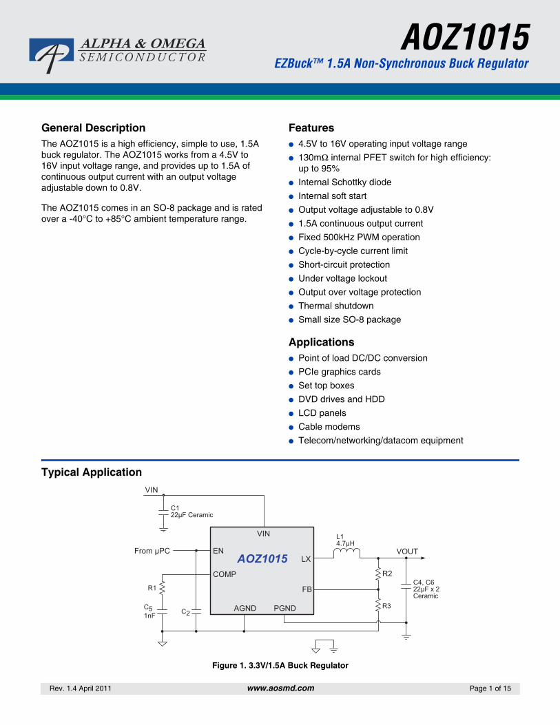
Pin Configuration
Pin Description
Part Number Ambient Temperature Range Package Environmental
AOZ1015AI -40°C to +85°C SO-8 RoHS
LX
LX
EN
COMP
1
2
3
4
PGND
VIN
AGND
FB
SO-8 (Top View)
8
7
6
5
Pin Number Pin Name Pin Function1 PGND Power ground. Electrically needs to be connected to AGND.
2 VIN Supply voltage input. When VIN rises above the UVLO threshold the device starts up.
3 AGND Reference connection for controller section. Also used as thermal connection for controller section. Electrically needs to be connected to PGND.
4 FB The FB pin is used to determine the output voltage via a resistor divider between the output and GND.
5 COMP External loop compensation pin.
6 EN The enable pin is active HIGH. Connect EN pin to VIN if not used. Do not leave the EN pin floating.
7, 8 LX PWM output connection to inductor. Thermal connection for output stage.
AOZ1015
Rev. 1.4 April 2011 www.aosmd.com Page 3 of 15
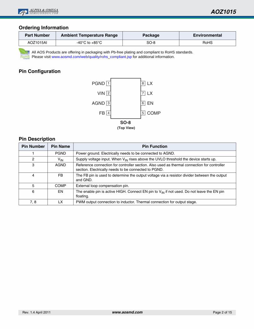
Block Diagram
Absolute Maximum RatingsExceeding the Absolute Maximum ratings may damage the device.
Note:1. Devices are inherently ESD sensitive, handling precautions are
required. Human body model rating: 1.5kΩ in series with 100pF. The machine model is a 200pF capacitor discharged directly into each pin.
Recommend Operating RatingsThe device is not guaranteed to operate beyond the Maximum Operating Ratings.
Note:2. The value of ΘJA is measured with the device mounted on 1-in2 FR-4
board with 2oz. Copper, in a still air environment with TA = 25°C. The value in any given application depends on the user’s specific board design.
500kHz/38kHzOscillator
AGND PGND
VIN
EN
FB
COMP
LX
OTPInternal+5V
ILimit
PWMControlLogic
5V LDORegulator
UVLO& POR
SoftstartReference& Bias
0.8V
Q1
PWMComp
LevelShifter
+FET
Driver
ISen
EAmp
0.2V
+
–
+
–
+
–
+
–
+
0.96V
Frequency Foldback
Comparator
Over VoltageProtection
Comparator+
–
Parameter Rating
Supply Voltage (VIN) 18V
LX to AGND -0.7V to VIN+0.3V
EN to AGND -0.3V to VIN+0.3V
FB to AGND -0.3V to 6V
COMP to AGND -0.3V to 6V
PGND to AGND -0.3V to +0.3V
Junction Temperature (TJ) +150°C
Storage Temperature (TS) -65°C to +150°C
ESD Rating(1)
Human Body ModelMachine Model
2kV200V
Parameter Rating
Supply Voltage (VIN) 4.5V to 16V
Output Voltage Range 0.8V to VIN
Ambient Temperature (TA) -40°C to +85°C
Package Thermal Resistance SO-8(ΘJA)(2)
87°C/W
AOZ1015
Rev. 1.4 April 2011 www.aosmd.com Page 4 of 15
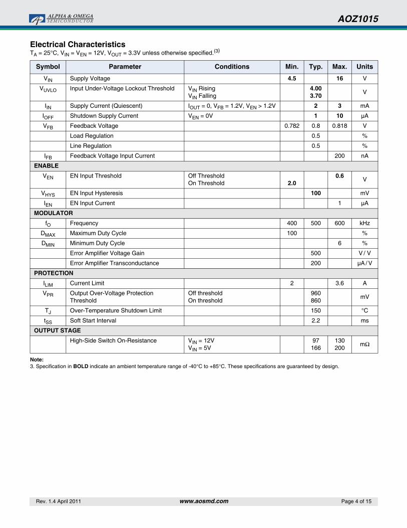
Electrical CharacteristicsTA = 25°C, VIN = VEN = 12V, VOUT = 3.3V unless otherwise specified.(3)
Note:3. Specification in BOLD indicate an ambient temperature range of -40°C to +85°C. These specifications are guaranteed by design.
Symbol Parameter Conditions Min. Typ. Max. Units
VIN Supply Voltage 4.5 16 V
VUVLO Input Under-Voltage Lockout Threshold VIN RisingVIN Falling
4.003.70 V
IIN Supply Current (Quiescent) IOUT = 0, VFB = 1.2V, VEN > 1.2V 2 3 mA
IOFF Shutdown Supply Current VEN = 0V 1 10 µA
VFB Feedback Voltage 0.782 0.8 0.818 V
Load Regulation 0.5 %
Line Regulation 0.5 %
IFB Feedback Voltage Input Current 200 nA
ENABLE
VEN EN Input Threshold Off ThresholdOn Threshold 2.0
0.6 V
VHYS EN Input Hysteresis 100 mV
IEN EN Input Current 1 µA
MODULATOR
fO Frequency 400 500 600 kHz
DMAX Maximum Duty Cycle 100 %
DMIN Minimum Duty Cycle 6 %
Error Amplifier Voltage Gain 500 V / V
Error Amplifier Transconductance 200 µA / V
PROTECTION
ILIM Current Limit 2 3.6 A
VPR Output Over-Voltage Protection Threshold
Off thresholdOn threshold
960860 mV
TJ Over-Temperature Shutdown Limit 150 °C
tSS Soft Start Interval 2.2 ms
OUTPUT STAGE
High-Side Switch On-Resistance VIN = 12VVIN = 5V
97166
130200 mΩ
AOZ1015
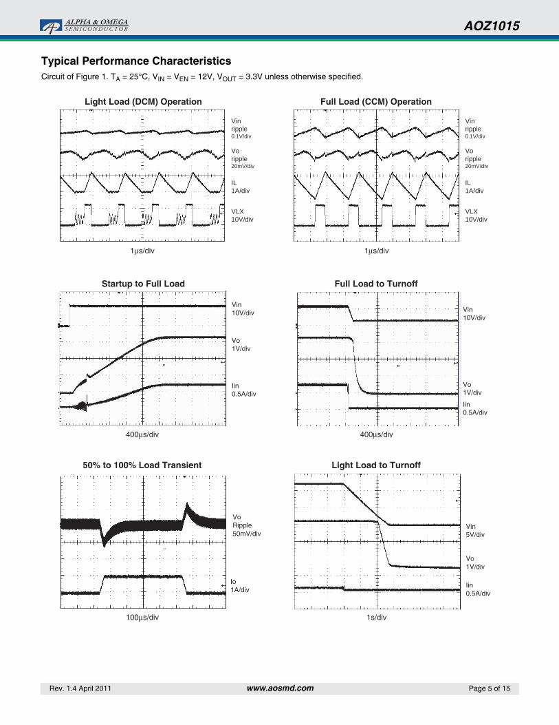
Typical Performance Characteristics Circuit of Figure 1. TA = 25°C, VIN = VEN = 12V, VOUT = 3.3V unless otherwise specified.
Light Load (DCM) Operation Full Load (CCM) Operation
Startup to Full Load Full Load to Turnoff
50% to 100% Load Transient Light Load to Turnoff
1μs/div 1μs/div
400μs/div 400μs/div
100μs/div 1s/div
Vin10V/div
Vo1V/div
Iin0.5A/div
Vo Ripple
Io1A
50mV/div
/div
Vin ripple0.1V/div
Vo ripple20mV/div
IL1A/div
VLX10V/div
Vin ripple0.1V/div
Vo ripple20mV/div
IL1A/div
VLX10V/div
Vin10V/div
Vo1V/div
Iin0.5A/div
Vin5V/div
Vo1V/div
Iin0.5A/div
Rev. 1.4 April 2011 www.aosmd.com Page 5 of 15
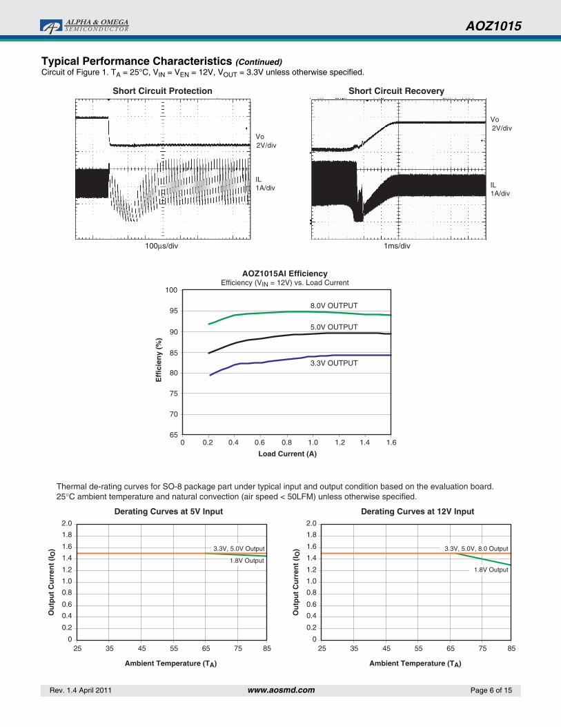
AOZ1015
Typical Performance Characteristics (Continued)Circuit of Figure 1. TA = 25°C, VIN = VEN = 12V, VOUT = 3.3V unless otherwise specified.
Vo2V/div
IL1A/div
Vo2V/div
IL1A/div
Short Circuit Protection Short Circuit Recovery
100μs/div 1ms/div
Derating Curves at 5V Input
AOZ1015AI EfficiencyEfficiency (VIN = 12V) vs. Load Current
3.3V OUTPUT
5.0V OUTPUT
8.0V OUTPUT
0 0.2 0.4 0.6 0.8 1.0 1.2 1.4 1.6
Load Current (A)
Ambient Temperature (TA)
80
75
70
65
85
90
95
100
Eff
icie
ny
(%)
Ou
tpu
t C
urr
ent
(IO
)
Derating Curves at 12V Input
3.3V, 5.0V Output
1.8V Output
Thermal de-rating curves for SO-8 package part under typical input and output condition based on the evaluation board.25°C ambient temperature and natural convection (air speed < 50LFM) unless otherwise specified.
0
0.2
0.4
0.6
0.8
1.0
1.2
1.4
1.6
1.8
2.0
25 35 45 55 65 75 85
Ambient Temperature (TA)
Ou
tpu
t C
urr
ent
(IO
) 3.3V, 5.0V, 8.0 Output
1.8V Output
0
0.2
0.4
0.6
0.8
1.0
1.2
1.4
1.6
1.8
2.0
25 35 45 55 65 75 85
Rev. 1.4 April 2011 www.aosmd.com Page 6 of 15
AOZ1015
Detailed DescriptionThe AOZ1015 is a current-mode step down regulator with integrated high side PMOS switch and a low side freewheeling Schottky diode. It operates from a 4.5V to 16V input voltage range and supplies up to 1.5A of load current. The duty cycle can be adjusted from 6% to 100% allowing a wide range of output voltages. Features include; enable control, Power-On Reset, input under voltage lockout, fixed internal soft-start and thermal shut down.
The AOZ1015 is available in an SO-8 package.
Enable and Soft StartThe AOZ1015 has an internal soft start feature to limit in-rush current and ensure the output voltage ramps up smoothly to regulation voltage. A soft start process begins when the input voltage rises to 4.0V and voltage on EN pin is HIGH. In the soft start process, the output voltage is typically ramped to regulation voltage in 2.2ms. The 2.2ms soft start time is set internally.
The EN pin of the AOZ1015 is active HIGH. Connect the EN pin to VIN if the enable function is not used. Pulling EN to ground will disable the AOZ1015. Do not leave it open. The voltage on the EN pin must be above 2.0V to enable the AOZ1015. When voltage on EN falls below 0.6V, the AOZ1015 is disabled. If an application circuit requires the AOZ1015 to be disabled, an open drain or open collector circuit should be used to interface to EN pin.
Steady-State OperationUnder steady-state conditions, the converter operates in fixed frequency and Continuous-Conduction Mode (CCM).
The AOZ1015 integrates an internal P-MOSFET as the high-side switch. Inductor current is sensed by amplifying the voltage drop across the drain to source of the high side power MOSFET. Output voltage is divided down by the external voltage divider at the FB pin. The difference of the FB pin voltage and reference is amplified by the internal transconductance error amplifier. The error voltage, which shows on the COMP pin, is compared against the current signal, which is the sum of inductor current signal and ramp compensation signal, at PWM comparator input. If the current signal is less than the error voltage, the internal high-side switch is on. The inductor current flows from the input through the inductor to the output. When the current signal exceeds the error voltage, the high-side switch is off. The inductor current is freewheeling through the internal Schottky diode to output.
The AOZ1015 uses a P-Channel MOSFET as the high side switch. It saves the bootstrap capacitor normally seen in a circuit which is using an NMOS switch. It allows 100% turn-on of the upper switch to achieve linear regu-lation mode of operation. The minimum voltage drop from VIN to VO is the load current X DC resistance of MOSFET + DC resistance of the buck inductor. It can be calculated by equation below:
where;
VO_MAX is the maximum output voltage,
VIN is the input voltage from 4.5V to 16V,
IO is the output current from 0A to 1.5A,
RDS(ON) is the on resistance of the internal MOSFET, the value is between 97mΩ and 200mΩ depending on input voltage and junction temperature, and
Rinductor is the inductor DC resistance.
Switching FrequencyThe AOZ1015 switching frequency is fixed and set by an internal oscillator. The actual switching frequency could range from 400kHz to 600kHz due to device variation.
Output Voltage ProgrammingOutput voltage can be set by feeding back the output to the FB pin with a resistor divider network. In the application circuit shown in Figure 1. The resistor divider network includes R2 and R3. Usually, a design is started by picking a fixed R3 value and calculating the required R2 with equation below.
Some standard values of R2, R3 for most commonly used output voltage values are listed in Table 1.
Table 1.
VO (V) R2 (kΩ) R3 (kΩ)
0.8 1.0 Open
1.2 4.99 10
1.5 10 11.5
1.8 12.7 10.2
2.5 21.5 10
3.3 31.6 10
5.0 52.3 10
VO_MAX VIN IO RDS ON( ) Rinductor+( )×–=
VO 0.8 1R2
R3-------+
⎝ ⎠⎜ ⎟⎛ ⎞
×=
Rev. 1.4 April 2011 www.aosmd.com Page 7 of 15
AOZ1015
The combination of R2 and R3 should be large enough to avoid drawing excessive current from the output, which will cause power loss.
Since the switch duty cycle can be as high as 100%, the maximum output voltage can be set as high as the input voltage minus the voltage drop on upper PMOS and inductor.
Protection FeaturesThe AOZ1015 has multiple protection features to prevent system circuit damage under abnormal conditions.
Over Current Protection (OCP)The sensed inductor current signal is also used for over current protection. Since the AOZ1015 employs peak current mode control, the COMP pin voltage is proportional to the peak inductor current. The COMP pin voltage is limited to be between 0.4V and 2.5V internally. The peak inductor current is automatically limited cycle by cycle.
The cycle by cycle current limit threshold is set between 2.5A and 3.6A. When the load current reaches the current limit threshold, the cycle by cycle current limit circuit turns off the high side switch immediately to terminate the current duty cycle. The inductor current stop rising. The cycle by cycle current limit protection directly limits inductor peak current. The average induc-tor current is also limited due to the limitation on peak inductor current. When cycle by cycle current limit circuit is triggered, the output voltage drops as the duty cycle decreases.
The AOZ1015 has internal short circuit protection to protect itself from catastrophic failure under output short circuit conditions. The FB pin voltage is proportional to the output voltage. Whenever FB pin voltage is below 0.2V, the short circuit protection circuit is triggered. As a result, the converter is shut down and hiccups at a frequency equal to 1/8 of normal switching frequency. The converter will start up via a soft start once the short circuit condition is resolved. In short circuit protection mode, the inductor average current is greatly reduced because of the low hiccup frequency.
Output Over Voltage Protection (OVP)The AOZ1015 monitors the feedback voltage. When the feedback voltage is higher than 960mV, it immediately turns-off the PMOS to protect the output voltage overshoot at fault condition. When feedback voltage is lower than 940mV, the PMOS is allowed to turn on in the next cycle.
Power-On Reset (POR)A power-on reset circuit monitors the input voltage. When the input voltage exceeds 4V, the converter starts operation. When input voltage falls below 3.7V, the converter will stop switching.
Thermal ProtectionAn internal temperature sensor monitors the junction temperature. It shuts down the internal control circuit and high side PMOS if the junction temperature exceeds 150°C.
Application InformationThe basic AOZ1015 application circuit is shown in Figure 1. Component selection is explained below.
Input CapacitorThe input capacitor (C1 in Figure 1) must be connected to the VIN pin and PGND pin of the AOZ1015 to maintain steady input voltage and filter out the pulsing input current. A small decoupling capacitor (Cd in Figure 1), usually 1µF, should be connected to the VIN pin and AGND pin for stable operation of the AOZ1015. The voltage rating of input capacitor must be greater than maximum input voltage plus ripple voltage.
The input ripple voltage can be approximated by equa-tion below:
Since the input current is discontinuous in a buck converter, the current stress on the input capacitor is another concern when selecting the capacitor. For a buck circuit, the RMS value of input capacitor current can be calculated by:
If let m equal the conversion ratio:
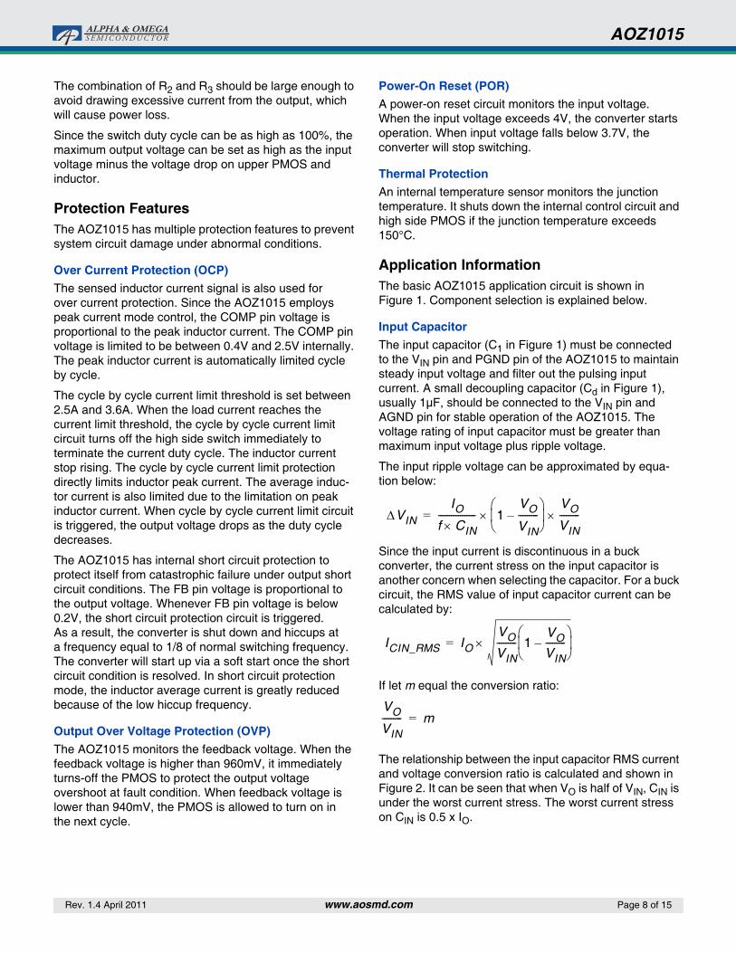
The relationship between the input capacitor RMS current and voltage conversion ratio is calculated and shown in Figure 2. It can be seen that when VO is half of VIN, CIN is under the worst current stress. The worst current stress on CIN is 0.5 x IO.
ΔVINIO
f CIN×----------------- 1
VO
VIN---------–
⎝ ⎠⎜ ⎟⎛ ⎞ VO
VIN---------××=
ICIN_RMS IOVOVIN--------- 1
VOVIN---------–
⎝ ⎠⎜ ⎟⎛ ⎞
×=
VO
VIN--------- m=
Rev. 1.4 April 2011 www.aosmd.com Page 8 of 15
AOZ1015
Figure 2. ICIN vs. Voltage Conversion Ratio
For reliable operation and best performance, the input capacitors must have current rating higher than ICIN_RMS at the worst operating conditions. Ceramic capacitors are preferred for input capacitors because of their low ESR and high ripple current rating. Depending on the application circuits, other low ESR tantalum capacitors or aluminum electrolytic capacitors may also be used. When selecting ceramic capacitors, X5R or X7R type dielectric ceramic capacitors are preferred for their better temperature and voltage characteristics. Note that the ripple current rating from capacitor manufacturers is based on a certain device life time. Further de-rating may be necessary for practical design requirement.
InductorThe inductor is used to supply constant current to output when it is driven by a switching voltage. For a given input and output voltage, inductance and switching frequency together decide the inductor ripple current, which is:
The peak inductor current is:
High inductance gives low inductor ripple current but requires a larger size inductor to avoid saturation. Low ripple current reduces inductor core losses. It also reduces RMS current through the inductor and switches, which results in less conduction loss. Usually, peak to peak ripple current on inductor is designed to be 20% to 30% of output current.
When selecting the inductor, make sure it is able to handle the peak current without saturation even at the highest operating temperature.
The inductor takes the highest current in a buck circuit. The conduction loss on inductor needs to be checked for thermal and efficiency requirements.
Surface mount inductors in different shape and styles are available from Coilcraft, Elytone and Murata. Shielded inductors are small and radiate less EMI noise. They cost more than unshielded inductors. The choice depends on EMI requirement, price and size.
Output CapacitorThe output capacitor is selected based on the DC output voltage rating, output ripple voltage specification and ripple current rating.
The selected output capacitor must have a higher rated voltage specification than the maximum desired output voltage including ripple. De-rating needs to be consid-ered for long term reliability.
Output ripple voltage specification is another important factor for selecting the output capacitor. In a buck converter circuit, output ripple voltage is determined by inductor value, switching frequency, output capacitor value and ESR. It can be calculated by the equation below:
where,
CO is output capacitor value, and
ESRCO is the equivalent series resistance of the output capacitor.
When a low ESR ceramic capacitor is used as an output capacitor, the impedance of the capacitor at the switch-ing frequency dominates. Output ripple is primarily caused by capacitor value and inductor ripple current. The output ripple voltage calculation can be simplified to:
If the impedance of ESR at switching frequency dominates, the output ripple voltage is primarily decided by capacitor ESR and inductor ripple current. The output ripple voltage calculation can be further simplified to:
For lower output ripple voltage across the entire operating temperature range, X5R or X7R dielectric type of ceramic, or other low ESR tantalum are recommended to be used as output capacitors.
0
0.1
0.2
0.3
0.4
0.5
0 0.5 1m
ICIN_RMS(m)
IO
ΔILVO
f L×----------- 1
VOVIN
---------–⎝ ⎠⎜ ⎟⎛ ⎞
×=
ILpeak IOΔIL2--------+=
ΔVO ΔIL ESRCO1
8 f CO××-------------------------+⎝ ⎠
⎛ ⎞×=
ΔVO ΔIL1
8 f CO××-------------------------×=
ΔVO ΔIL ESRCO×=
Rev. 1.4 April 2011 www.aosmd.com Page 9 of 15
AOZ1015
In a buck converter, output capacitor current is continuous. The RMS current of the output capacitor is decided by the peak to peak inductor ripple current. It can be calculated by:
Usually, the ripple current rating of the output capacitor is a smaller issue because of the low current stress. When the buck inductor is selected to be very small and inductor ripple current is high, the output capacitor could be overstressed.
Loop CompensationThe AOZ1015 employs peak current mode control for easy use and fast transient response. Peak current mode control eliminates the double pole effect of the output L&C filter. It greatly simplifies the compensation loop design.
With peak current mode control, the buck power stage can be simplified to be a one-pole and one-zero system in frequency domain. The pole is the dominant pole and can be calculated by:
The zero is a ESR zero due to output capacitor and its ESR. It is can be calculated by:
where;
CO is the output filter capacitor,
RL is load resistor value, and
ESRCO is the equivalent series resistance of output capacitor.
The compensation design is actually to shape the converter close loop transfer function to get the desired gain and phase. Several different types of compensation networks can be used for the AOZ1015. In most cases, a series capacitor and resistor network connected to the COMP pin sets the pole-zero and is adequate for a stable high-bandwidth control loop.
The FB pin and the COMP pin are the inverting input and the output of the internal transconductance error amplifier. A series R and C compensation network connected to COMP provides one pole and one zero. The pole is:
where;
GEA is the error amplifier transconductance, which is 200 x 10-6 A/V,
GVEA is the error amplifier voltage gain, which is 500 V/V, and
CC is compensation capacitor.
The zero given by the external compensation network, capacitor CC (C5 in Figure 1) and resistor RC (R1 in Figure 1), is located at:
To design the compensation circuit, a target crossover frequency fC for close loop must be selected. The system crossover frequency is where the control loop has unity gain. The crossover frequency is also called the converter bandwidth. Generally, a higher bandwidth means faster response to load transient. However, the bandwidth should not be too high due to system stability concern. When designing the compensation loop, converter stability under all line and load conditions must be considered.
Usually, it is recommended to set the bandwidth to be less than 1/10 of the switching frequency. The AOZ1015 operates at a fixed switching frequency range from 350kHz to 600kHz. It is recommended to choose a crossover frequency less than 30kHz.
The strategy for choosing RC and CC is to set the cross over frequency with RC and set the compensator zero with CC. Using selected crossover frequency, fC, to calculate RC:
where;
fC is the desired crossover frequency,
VFB is 0.8V,
GEA is the error amplifier transconductance, which is 200 x 10-6 A/V, and
GCS is the current sense circuit transconductance, which is 5.64 A/V.
The compensation capacitor CC and resistor RC together make a zero. This zero is put somewhere close to the dominate pole fp1 but lower than 1/5 of selected crossover frequency. CC can is selected by:
ICO_RMSΔIL
12----------=
fP11
2π CO RL××-----------------------------------=
fZ11
2π CO ESRCO××------------------------------------------------=
fP2GEA
2π CC GVEA××-------------------------------------------=
fZ21
2π CC RC××-----------------------------------=
fC 30kHz=
RC fCVO
VFB----------
2π CO×
GEA GCS×------------------------------××=
CC1.5
2π RC fP1××-----------------------------------=
Rev. 1.4 April 2011 www.aosmd.com Page 10 of 15
AOZ1015
The previous equation above can also be simplified to:
An easy-to-use application software which helps to design and simulate the compensation loop can be found at www.aosmd.com.
Thermal Management and Layout ConsiderationIn the AOZ1015 buck regulator circuit, high pulsing current flows through two circuit loops. The first loop starts from the input capacitors, to the VIN pin, to the LX pins, to the filter inductor, to the output capacitor and load, and then returns to the input capacitor through ground. Current flows in the first loop when the high side switch is on. The second loop starts from inductor, to the output capacitors and load, to the PGND pin of the AOZ1015, to the LX pins of the AOZ1015. Current flows in the second loop when the low side diode is on.
In PCB layout, minimizing the two loops area reduces the noise of this circuit and improves efficiency. A ground plane is recommended to connect input capacitor, output capacitor, and PGND pin of the AOZ1015.
In the AOZ1015 buck regulator circuit, the two major power dissipating components are the AOZ1015 and the output inductor. The total power dissipation of converter circuit can be measured by input power minus output power.
The power dissipation of the inductor can be approxi-mately calculated by output current and DCR of inductor.
The actual AOZ1015 junction temperature can be calculated with power dissipation in the AOZ1015 and thermal impedance from junction to ambient.
The maximum junction temperature of the AOZ1015 is 150°C, which limits the maximum load current capability. Please see the thermal de-rating curves for the maximum load current of the AOZ1015 under different ambient temperatures.
The thermal performance of the AOZ1015 is strongly affected by the PCB layout. Extra care should be taken by users during the design process to ensure that the IC will operate under the recommended environmental conditions.
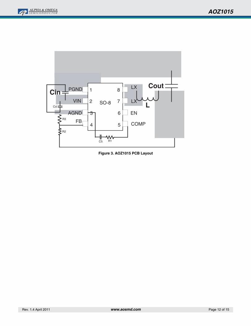
Several layout tips are listed below for the best electronic and thermal performance. Figure 3 illustrates a single layer PCB layout example as reference.
1. Do not use thermal relief connection to the VIN and the PGND pins. Pour a maximized copper area to the PGND pin and the VIN pin to help thermal dissipation.
2. The input capacitors should be connected as close as possible to the VIN and PGND pins.
3. A ground plane is preferred. If a ground plane is not used, separate PGND from AGND and connect them only at one point to avoid the PGND pin noise coupling to the AGND pin. In this case, a decoupling capacitor should be connected between VIN and AGND.
4. Make the current trace from LX pins to L to CO to the PGND as short as possible.
5. Pour copper plane on all unused board area and connect it to stable DC nodes, like VIN, GND or VOUT.
6. The two LX pins are connected to the internal PFET drain. They are low resistance thermal conduction path and a noisy switching node. Connecting a copper plane to the LX pin to help thermal dissipa-tion. This copper plane should not be too large otherwise switching noise may be coupled to other parts of the circuit.
7. Keep sensitive signal traces such as trace connecting FB and COMP away from the LX pins.
CCCO RL×
RC
---------------------=
Ptotal_loss VIN IIN VO IO×–×=
Pinductor_loss IO2 Rinductor 1.1××=
Tjunction Ptotal_loss Pinductor_loss–( ) Θ×=Tambient+ +
Rev. 1.4 April 2011 www.aosmd.com Page 11 of 15
AOZ1015
Figure 3. AOZ1015 PCB Layout
SO-8
1
2
3
4
8
7
6
5
VIN
AGND
COMP
LX
LX
EN
FB
Cout
C5 R1
R3
R2
L
Cin PGND
Cd
Rev. 1.4 April 2011 www.aosmd.com Page 12 of 15
AOZ1015
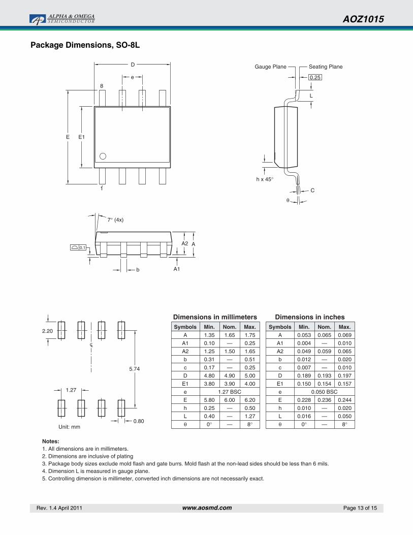
Package Dimensions, SO-8L
Notes:1. All dimensions are in millimeters.2. Dimensions are inclusive of plating3. Package body sizes exclude mold flash and gate burrs. Mold flash at the non-lead sides should be less than 6 mils.4. Dimension L is measured in gauge plane.5. Controlling dimension is millimeter, converted inch dimensions are not necessarily exact.
Symbols
A
A1
A2
b
c
D
E1
e
E
h
L
θ
Dimensions in millimetersMin.
1.35
0.10
1.25
0.31
0.17
4.80
3.80
5.80
0.25
0.40
0°
D
C
L
h x 45°
7° (4x)
b
2.20
5.74
0.80Unit: mm
1.27
A1
A2 A0.1
θ
Gauge Plane Seating Plane
0.25e
8
1
E1E
Nom.
1.65
—
1.50
—
—
4.90
3.90
1.27 BSC
6.00
—
—
—
Max.
1.75
0.25
1.65
0.51
0.25
5.00
4.00
6.20
0.50
1.27
8°
Symbols
A
A1
A2
b
c
D
E1
e
E
h
L
θ
Dimensions in inchesMin.
0.053
0.004
0.049
0.012
0.007
0.189
0.150
0.228
0.010
0.016
0°
Nom.
0.065
—
0.059
—
—
0.193
0.154
0.050 BSC
0.236
—
—
—
Max.
0.069
0.010
0.065
0.020
0.010
0.197
0.157
0.244
0.020
0.050
8°
Rev. 1.4 April 2011 www.aosmd.com Page 13 of 15
AOZ1015
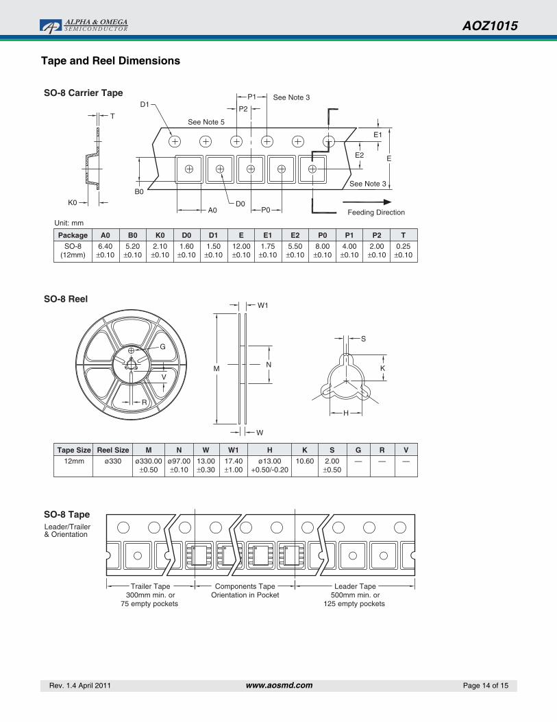
Tape and Reel Dimensions
SO-8 Carrier Tape
SO-8 Reel
SO-8 TapeLeader/Trailer& Orientation
Tape Size
12mm
Reel Size
ø330
M
ø330.00±0.50
Package
SO-8(12mm)
A0
6.40±0.10
B0
5.20±0.10
K0
2.10±0.10
D0
1.60±0.10
D1
1.50±0.10
E
12.00±0.10
E1
1.75±0.10
E2
5.50±0.10
P0
8.00±0.10
P1
4.00±0.10
P2
2.00±0.10
T
0.25±0.10
N
ø97.00±0.10
K0
Unit: mm
B0
G
M
W1
S
K
H
N
W
V
R
Trailer Tape300mm min. or
75 empty pockets
Components TapeOrientation in Pocket
Leader Tape500mm min. or
125 empty pockets
A0
P1
P2
See Note 5
See Note 3
See Note 3
Feeding DirectionP0
E2
E1
E
D0
T
D1
W
13.00±0.30
W1
17.40±1.00
H
ø13.00+0.50/-0.20
K
10.60
S
2.00±0.50
G
—
R
—
V
—
Rev. 1.4 April 2011 www.aosmd.com Page 14 of 15
AOZ1015
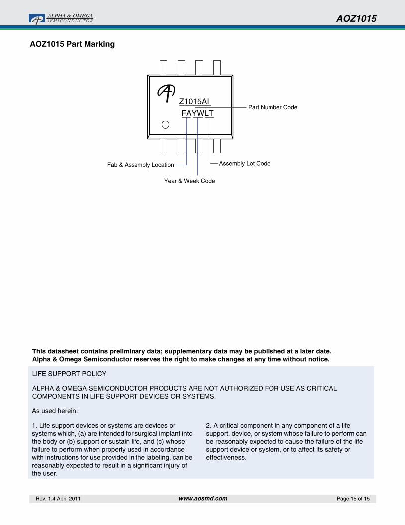
AOZ1015 Part Marking
Z1015AI
FAYPart Number Code
Assembly Lot CodeFab & Assembly Location
Year & Week Code
WLT
As used herein:
1. Life support devices or systems are devices or systems which, (a) are intended for surgical implant into the body or (b) support or sustain life, and (c) whose failure to perform when properly used in accordance with instructions for use provided in the labeling, can be reasonably expected to result in a significant injury of the user.
2. A critical component in any component of a life support, device, or system whose failure to perform can be reasonably expected to cause the failure of the life support device or system, or to affect its safety or effectiveness.
This datasheet contains preliminary data; supplementary data may be published at a later date. Alpha & Omega Semiconductor reserves the right to make changes at any time without notice.
LIFE SUPPORT POLICY
ALPHA & OMEGA SEMICONDUCTOR PRODUCTS ARE NOT AUTHORIZED FOR USE AS CRITICAL COMPONENTS IN LIFE SUPPORT DEVICES OR SYSTEMS.
Rev. 1.4 April 2011 www.aosmd.com Page 15 of 15