Embed Size (px)
Citation preview

10. A. Schirotzek, C.-H. Wu, A. Sommer, M. W. Zwierlein,Phys. Rev. Lett. 102, 230402 (2009).
11. S. Nascimbène et al., Phys. Rev. Lett. 103, 170402(2009).
12. C. Kohstall et al., Nature 485, 615–618 (2012).13. M. Koschorreck et al., Nature 485, 619–622 (2012).14. Y. Zhang, W. Ong, I. Arakelyan, J. E. Thomas, Phys. Rev. Lett.
108, 235302 (2012).15. P. Massignan, M. Zaccanti, G. M. Bruun, Rep. Prog. Phys. 77,
034401 (2014).16. M. Sidler et al., http://arXiv.org/abs/1603.09215 (2016).17. J. Goold, T. Fogarty, N. Lo Gullo, M. Paternostro, T. Busch,
Phys. Rev. A 84, 063632 (2011).18. M. Knap et al., Phys. Rev. X 2, 041020 (2012).19. M. Cetina et al., Phys. Rev. Lett. 115, 135302 (2015).20. See supplementary materials on Science Online.21. D. Naik et al., Eur. Phys. J. D 65, 55–65 (2011).22. J. Loschmidt, Sitzungsber. Akad. Wissenschaften Wien 73,
128 (1876).23. E. L. Hahn, Phys. Rev. 80, 580–594 (1950).
24. P. Nozières, C. T. De Dominicis, Phys. Rev. 178, 1097–1107 (1969).25. R. A. Jalabert, H. M. Pastawski, Adv. Solid State Phys. 41,
483–496 (2001).26. F. Chevy, Phys. Rev. A 74, 063628 (2006).27. X. Cui, H. Zhai, Phys. Rev. A 81, 041602 (2010).28. J. Dubois et al., Nature 502, 659–663 (2013).29. C. Mora, F. Chevy, Phys. Rev. Lett. 104, 230402 (2010).30. Z. Yu, S. Zöllner, C. J. Pethick, Phys. Rev. Lett. 105, 188901
(2010).31. W. Zwerger, Ed., The BCS-BEC Crossover and the Unitary
Fermi Gas (Springer, 2012).32. R. A. Hart et al., Nature 519, 211–214 (2015).33. L. J. LeBlanc, J. H. Thywissen, Phys. Rev. A 75, 053612 (2007).
ACKNOWLEDGMENTS
We thank M. Baranov, F. Schreck, G. Bruun, N. Davidson, andR. Folman for stimulating discussions. Supported by NSF througha grant for ITAMP at Harvard University and the SmithsonianAstrophysical Observatory (R.S.); the Technical University ofMunich-Institute for Advanced Study, funded by the German
Excellence Initiative and the European Union FP7 under grantagreement 291763 (M.K.); the Harvard-MIT Center for UltracoldAtoms, NSF grant DMR-1308435, the Air Force Office of ScientificResearch Quantum Simulation Multidisciplinary UniversityResearch Initiative (MURI), the Army Research Office MURI onAtomtronics, M. Rössler, the Walter Haefner Foundation, the ETHFoundation, and the Simons Foundation (E.D.); and the AustrianScience Fund (FWF) within the SFB FoQuS (F4004-N23) andwithin the DK ALM (W1259-N27).
SUPPLEMENTARY MATERIALS
www.sciencemag.org/content/354/6308/96/suppl/DC1Materials and MethodsSupplementary TextFigs. S1 to S11Table S1References (34–56)
20 February 2016; accepted 6 September 201610.1126/science.aaf5134
DEVICE TECHNOLOGY
MoS2 transistors with 1-nanometergate lengthsSujay B. Desai,1,2,3 Surabhi R. Madhvapathy,1,2 Angada B. Sachid,1,2
Juan Pablo Llinas,1,2 Qingxiao Wang,4 Geun Ho Ahn,1,2 Gregory Pitner,5 Moon J. Kim,4
Jeffrey Bokor,1,2 Chenming Hu,1 H.-S. Philip Wong,5 Ali Javey1,2,3*
Scaling of silicon (Si) transistors is predicted to fail below 5-nanometer (nm) gatelengths because of severe short channel effects. As an alternative to Si, certain layeredsemiconductors are attractive for their atomically uniform thickness down to amonolayer, lower dielectric constants, larger band gaps, and heavier carrier effectivemass. Here, we demonstrate molybdenum disulfide (MoS2) transistors with a 1-nmphysical gate length using a single-walled carbon nanotube as the gate electrode. Theseultrashort devices exhibit excellent switching characteristics with near idealsubthreshold swing of ~65 millivolts per decade and an On/Off current ratio of~106. Simulations show an effective channel length of ~3.9 nm in the Off state and~1 nm in the On state.
As Si transistors rapidly approach their pro-jected scaling limit of ~5-nm gate lengths,exploration of new channel materials anddevice architectures is of utmost interest(1–3). This scaling limit arises from short
channel effects (4). Direct source-to-drain tunnel-ing and the loss of gate electrostatic control on thechannel severely degrade the Off state leakage cur-rents, thus limiting the scaling of Si transistors(5, 6). Certain semiconductor properties dictatethe magnitude of these effects for a given gatelength. Heavier carrier effective mass, largerband gap, and lower in-plane dielectric constantyield lower direct source-to-drain tunneling cur-rents (7). Uniform and atomically thin semicon-
ductors with low in-plane dielectric constantsare desirable for enhanced electrostatic controlof the gate. Thus, investigation and introduc-tion of semiconductors that have more ideal prop-erties than Si could lead to further scaling oftransistor dimensions with lower Off state dis-sipation power.Transition metal dichalcogenides (TMDs) are
layered two-dimensional (2D) semiconductorsthat have been widely explored as a potentialchannel material replacement for Si (8–11), andeach material exhibits different band struc-tures and properties (12–16). The layered natureof TMDs allows uniform thickness control withatomic-level precision down to the monolayerlimit. This thickness scaling feature of TMDsis highly desirable for well-controlled electro-statics in ultrashort transistors (3). For example,monolayer and few-layer MoS2 have been showntheoretically to be superior to Si at the sub-5-nmscaling limit (17, 18).The scaling characteristics of MoS2 and Si tran-
sistors as a function of channel thickness and gatelength are summarized in Fig. 1. We calculated
direct source-to-drain tunneling currents (ISD-LEAK)in the Off state for different channel lengths andthicknesses using a dual-gate device structure (fig.S1) as ameans to compare the twomaterials.MoS2shows more than two orders of magnitude reduc-tion in ISD-LEAK relative to Si mainly because ofits larger electron effective mass along the trans-port direction (m*
n ∼ 0:55m0 for MoS2 versusm*
n ∼ 0:19m0 for Si [100]) (19), with a trade-offresulting in lower ballistic On current. Notably,ISD-LEAK does not limit the scaling of monolayerMoS2 even down to the ~1-nm gate length, pre-senting a major advantage over Si [see more de-tails about calculations in the supplementarymaterials (20)]. Finally, few-layerMoS2 exhibits alower in-plane dielectric constant (~4) comparedwith bulk Si (~11.7), Ge (~16.2), and GaAs (~12.9),resulting in a shorter electrostatic characteristiclength (l) as depicted in fig. S2 (21).The above qualities collectively make MoS2 a
strong candidate for the channel material of fu-ture transistors at the sub-5-nm scaling limit.However, to date, TMD transistors at such smallgate lengths have not been experimentally ex-plored. Here, we demonstrate 1D gated, 2D semi-conductor field-effect transistors (1D2D-FETs) witha single-walled carbon nanotube (SWCNT) gate,aMoS2 channel, and physical gate lengths of ~1 nm.The 1D2D-FETs exhibit near ideal switching char-acteristics, including a subthreshold swing (SS) of~65mV per decade at room temperature and highOn/Off current ratios. The SWCNT diameter d ~1 nm for the gate electrode (22) minimized par-asitic gate to source-drain capacitance, which ischaracteristic of lithographically patterned tallgate structures. The~1-nmgate lengthof theSWCNTalso allowed for the experimental exploration ofthe device physics and properties of MoS2 tran-sistors as a function of semiconductor thickness(i.e., number of layers) at the ultimate gate-lengthscaling limit.The experimental device structure of the 1D2D-
FET (Fig. 2A) consists of a MoS2 channel (numberof layers vary), a ZrO2 gate dielectric, and a SWCNTgate on a 50-nm SiO2/Si substrate with a physi-cal gate length (LG ~ d) of ~1 nm. Long, alignedSWCNTs grown by chemical vapor deposition
SCIENCE sciencemag.org 7 OCTOBER 2016 • VOL 354 ISSUE 6308 99
1Electrical Engineering and Computer Sciences, University ofCalifornia, Berkeley, CA 94720, USA. 2Materials SciencesDivision, Lawrence Berkeley National Laboratory, Berkeley,CA 94720, USA. 3Berkeley Sensor and Actuator Center,University of California, Berkeley, CA 94720, USA.4Department of Materials Science and Engineering,University of Texas at Dallas, Richardson, TX 75080, USA.5Electrical Engineering, Stanford University, Stanford, CA94305, USA.*Corresponding author. Email: [email protected]
RESEARCH | REPORTS
on
Oct
ober
6, 2
016
http
://sc
ienc
e.sc
ienc
emag
.org
/D
ownl
oade
d fr
om

were transferred onto a n+ Si/SiO2 substrate(50-nm-thick SiO2) (23), located with a scanningelectron microscope (SEM), and contacted withpalladium via lithography andmetallization. Thesesteps were followed by atomic layer deposition(ALD) of ZrO2 and pick-and-place dry transfer ofMoS2 onto the SWCNT covered by ZrO2 (14).Nickel source and drain contacts were made toMoS2 to complete the device. The detailed pro-cess flow and discussion about device fabricationis provided in fig. S3.Figure 2B shows the optical image of a repre-
sentative 1D2D-FET capturing theMoS2 flake, thesource and drain contacts to MoS2, and the gatecontacts to the SWCNT. The SWCNTand theMoS2flake can be identified in the false-colored SEMimage of a representative sample (Fig. 2C). The1D2D-FET consists of four electrical terminals;source (S), drain (D), SWCNT gate (G), and the n+
Si substrate back gate (B). The SWCNT gate un-derlaps the S/D contacts. These underlapped re-gions were electrostatically doped by the Si backgate during the electrical measurements, therebyserving as n+ extension contact regions. The de-vice effectively operated like a junctionless tran-sistor (24), where the SWCNT gate locally depletedthe n+ MoS2 channel after applying a negativevoltage, thus turning Off the device.A cross-sectional transmission electron micro-
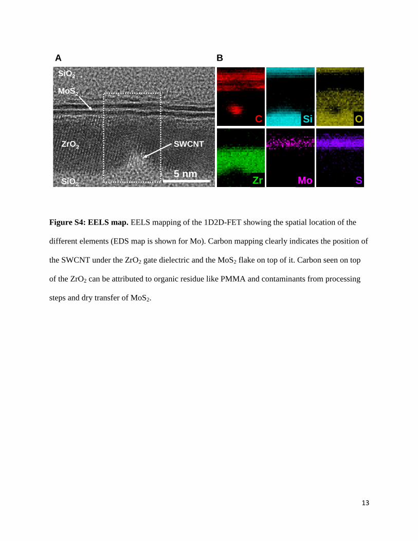
scope (TEM) image of a representative 1D2D-FET (Fig. 2D) shows the SWCNT gate, ZrO2 gatedielectric (thickness TOX~5.8 nm), and the bilayerMoS2 channel. The topography of ZrO2 surround-ing the SWCNT and the MoS2 flake on top of thegate oxide was flat, as seen in the TEM image. Thisgeometry is consistent with ALD nucleation ini-tiating on the SiO2 substrate surrounding theSWCNT and eventually covering it completely asthe thickness of deposited ZrO2 exceeds the SWCNTdiameter d (25). The spatial distribution of carbon,zirconium, and sulfur was observed in the electronenergy-loss spectroscopy (EELS) map of the de-vice region (Fig. 2E), thus confirming the loca-tion of the SWCNT, ZrO2, andMoS2 in the device(fig. S4) (20).The electrical characteristics for a 1D2D-FET
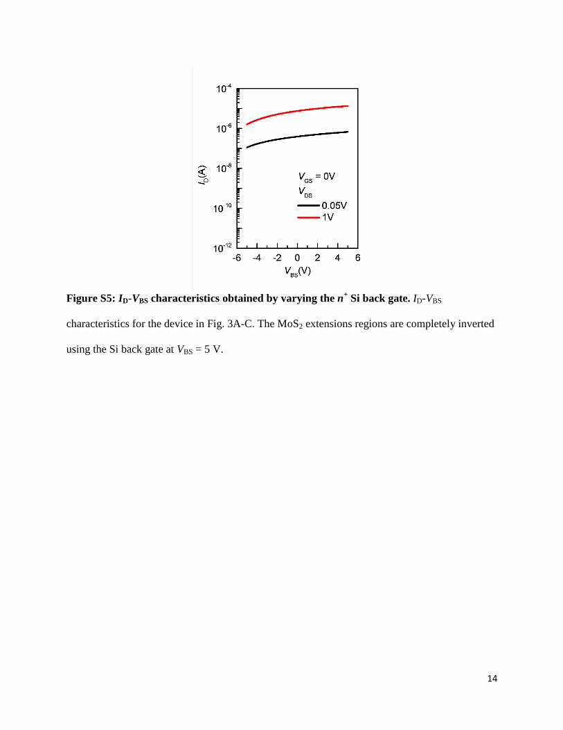
with a bilayerMoS2 channel (Fig. 3) show that theMoS2 extension regions (the underlapped regionsbetween the SWCNT gate and S/D contacts) couldbe heavily inverted (i.e., n+ state) by applying apositive back-gate voltage of VBS = 5 V to the Sisubstrate. The ID-VBS characteristics (fig. S5)indicate that the MoS2 flake was strongly in-verted by the back gate at VBS = 5 V. The ID-VGS
characteristics for the device atVBS = 5V andVDS =50mV and 1 V (Fig. 3A) demonstrate the ability ofthe ~1-nm SWCNT gate to deplete theMoS2 chan-nel and turn Off the device. The 1D2D-FET exhib-ited excellent subthreshold characteristics witha near ideal SS of ~65 mV per decade at roomtemperature and On/Off current ratio of ~106.The drain-induced barrier lowering (DIBL) was~290mV/V. Leakage currents through the SWCNTgate (IG) and the n+ Si back gate (IB) are at themeasurement noise level (Fig. 3A). The interfacetrap density (DIT) of the ZrO2-MoS2 interfaceestimated from SS was ~1.7 × 1012 cm−2 eV−1,
100 7 OCTOBER 2016 • VOL 354 ISSUE 6308 sciencemag.org SCIENCE
1 2 310 -14
10 -12
10 -10
10 -8
10 -6
10 -4
MoS2
I SD
-LE
AK (
A/µ
m)
TCH
(nm)
VGS
- VFB
= 0 V (OFF)
VDS
= 0.43 V
Si
TOX = 0.5 nm
ε OX,y = 3.9 ε0
LG = 4 nm
3 4 5 610 -20
10 -17
10 -14
10 -11
10 -8
10 -5
TCH
(nm)
Si: 2.17, 1.08MoS
2: 1.3, 0.65
I SD
-LE
AK (
A/µ
m)
LG (nm)
Low power technology limit
Fig. 1. Direct source-to-drain tunneling leakage current. (A) Normalized direct source-to-drain tunnel-ing leakage current (ISD-LEAK), calculated using the WKB (Wentzel-Kramers-Brillouin) approximation as afunction of channel thicknessTCH for Si andMoS2 in theOff state.VDS=VDD=0.43V from the InternationalTechnology Roadmap for Semiconductors (ITRS) 2026 technology node. (B) ISD-LEAK as a function of gatelength LG for different thicknesses of Si and MoS2 for the same Off state conditions as Fig. 1A.The dottedline in Fig. 1, A andB represents the lowoperating power limit for the 2026 technology node as specified bythe ITRS.
Fig. 2. 1D2D-FET device structure and characterization. (A) Schematic of 1D2D-FET with a MoS2
channel and SWCNTgate. (B) Optical image of a representative device shows the MoS2 flake, gate (G),source (S), and drain (D) electrodes. (C) False-colored SEM image of the device showing the SWCNT(blue), ZrO2 gate dielectric (green), MoS2 channel (orange), and the Ni source and drain electrodes(yellow). (D) Cross-sectional TEM image of a representative sample showing the SWCNTgate, ZrO2 gatedielectric, and bilayer MoS2 channel. (E) EELS map showing spatial distribution of carbon, zirconium, andsulfur in the device region, confirming the location of the SWCNT, MoS2 flake, and ZrO2 dielectric.
RESEARCH | REPORTS
on
Oct
ober
6, 2
016
http
://sc
ienc
e.sc
ienc
emag
.org
/D
ownl
oade
d fr
om

which is typical for transferred MoS2 flakes(26) because of the absence of surface danglingbonds (20).Figure 3B shows the ID-VDS characteristics at
different VGS values and fixed VBS = 5 V. The ID-VGS characteristics depended strongly on thevalue of VBS, which affects the extension regionresistance. The inversion of the extension regionsincreased with increasing VBS, thus reducing theseries resistance and contact resistance and ledto an increase in the On current and an improve-ment in the SS. At more positive values of VBS, VGShad to be more negative in order to deplete theMoS2 channel, which in turn made the thresholdvoltage (VT) more negative. AboveVBS = 1 V, the SSand IOn did not improve any further, and the ex-tension regionswere strongly inverted (Fig. 3C). Thus,the 1D2D-FET operated as a short-channel device.We performed detailed simulations using Sen-
taurus TCAD to understand the electrostatics ofthe 1D2D-FET. The Off and On state conditionscorrespond to (VGS-VT) of –0.3 V and 1.5 V, re-spectively (which give an On/Off current ratio of~106). The electric field contour plot (Fig. 3D) inthe Off state has a region of low electric field inthe MoS2 channel near the SWCNT, indicatingthat it is depleted. The reduced electron densityin the MoS2 channel (Fig. 3E), and the presenceof an energy barrier to electrons in the conduc-tion band (fig. S6A) are also consistent with theOff state of the device. The extension regions arestill under inversion because of the positive back-gate voltage. The electron density of the MoS2channel in the depletion region can be used todefine the effective channel length (LEFF) of the1D2D-FET, which is the region of channel con-trolled by the SWCNT gate (27–29). The channelis considered to be depleted if the electron den-sity falls below a defined threshold (nthreshold).The Off state LEFF, defined as the region of MoS2with electron density n < nthreshold (nthreshold = 1.3 ×105 cm−2), for this simulated 1D2D-FET is LEFF ~3.9 nm (Fig. 3E). LEFF is dependent on VGS and thevalue of nthreshold (fig. S7).As the device is turnedOff, the fringing electric
fields from the SWCNT (Fig. 3D) deplete fartherregions of the MoS2 channel and thus increaseLEFF. The short height of the naturally definedSWCNT gate prevents large fringing fields fromcontrolling the channel and hence achieves asmaller LEFF compared with lithographically pat-terned gates (fig. S8). The electric field and elec-tron density contours for the device in the Onstate confirm the strong inversion of the channelregion near the SWCNT (Fig. 3, F and G) withLEFF ~ LG = 1 nm. The energy bands in this caseare flat in the entire channel region (fig. S6B),with the On state current being limited by theresistance of the extension regions and mainlythe contacts. Doped S/D contacts along withshorter extension regions will result in increasedOn current.The effect of TOX scaling on short-channel
effects like DIBL was also studied using simu-lations (fig. S9). The electrostatics of the deviceimproves, and the influence of the drain on thechannel reduces, as TOX is scaled down to values
SCIENCE sciencemag.org 7 OCTOBER 2016 • VOL 354 ISSUE 6308 101
-3 -2 -1 0 110-12
10-10
10-8
10-6
10-4
VDS
= 1 V
I D (
A/µ
m)
VGS
(V)
VBS
-5 V -3 V -1 V 1 V 5 V
0.0 0.5 1.0 1.5 2.0 2.5
0
5
10
15
20
25
30 VGS
= -3 V to 0.5 V
Step = 0.5 VV
BS = 5 V
I D (
µA/µ
m)
VDS
(V)-3 -2 -1 0 1
10-12
10-10
10-8
10-6
10-4
IG, I
B
VDS
= 50 mV
VDS
= 1 V
I D (
A/µ
m)
VGS
(V)
VBS
= 5 V
65 mV/decade
e- density (cm-2)
6.5 x 10¹²
2.1 x 10⁹
1.3 x 10⁵SiO2
ZrO2
MoS2 ON
LEFF ~ 3.9 nm
SiO2
ZrO2
MoS2 OFF
(MV/cm)5.7
2.9
0.001SiO2
ZrO2
MoS2 ON
4 nmSiO2
ZrO2
MoS2 OFF
4 nm
4 nm 4 nm
SWCNT SWCNT
Fig. 3. Electrical characterization and TCAD simulations of 1D2D-FET. (A) ID-VGS characteristics of abilayer MoS2 channel SWCNTgated FETat VBS = 5 V and VDS = 50 mV and 1 V. The positive VBS voltageelectrostatically dopes the extension regions n+. (B) ID-VDS characteristic for the device at VBS = 5 V andvarying VGS. (C) ID-VGS characteristics at VDS = 1 Vand varying VBS illustrating the effect of back-gate biason the extension region resistance, SS, On current, and device characteristics. Electric field contour plotsfor a simulated bilayer MoS2 device using TCAD in the (D) Off and (F) On state. Electron density plots forthe simulated device using TCAD in the (E) Off and (G) On state. The electron density in the depletionregion is used to define the LEFF. LEFF ~ d ~ LG in the On state and LEFF > LG in the Off state because of thefringing electric fields from the SWCNTgate.
0 2 4 6 8 10 120
40
80
120
160
200
Simulation Experiment
VDS
= 1 V
VBS
= 5 V
Sub
thre
shol
d S
win
g (m
V/d
ec)
MoS2 thickness (nm)
-2 -1 0 1 210-13
10-11
10-9
10-7
10-5
I D (
A/µ
m)
VGS
-VT (V)
VBS
= 5 V
VDS
= 1 V
MoS2 thickness
1.3 nm 12 nm 31 nm
Fig. 4. MoS2 thickness dependence. (A) Dependence ofMoS2 channel thickness on the performance of1D2D-FET. SS increases with increasing MoS2 channel thickness. (B) Extracted SS from experimentalcurves and TCAD simulations show increasing SS as channel thickness TCH increases.
RESEARCH | REPORTS
on
Oct
ober
6, 2
016
http
://sc
ienc
e.sc
ienc
emag
.org
/D
ownl
oade
d fr
om

commensurate with LG. This effect is seen by thestrong dependence of DIBL on TOX, thus demon-strating the need for TOX scaling and high-k(dielectric constant) 2D dielectrics to furtherenhance the device performance.The effect of MoS2 thickness on the device
characteristics was systematically explored. At thescaling limit of the gate length, the semiconductorchannel thickness must also be scaled down ag-gressively, as described earlier. The electrostaticcontrol of the SWCNT gate on the MoS2 channeldecreasedwith increasing distance from theZrO2-MoS2 interface. Thus, as the MoS2 flake thicknesswas increased, the channel could not be complete-ly depleted by applying a negative VGS. Because ofthis effect, the SS for a 12-nm-thick MoS2 device(~170 mV per decade) was much larger than thatof bilayer MoS2 (~65 mV per decade), and as thethickness of MoS2 was increased to ~31 nm, thedevice could no longer be turned off (Fig. 4A).The experimental SS as a function of MoS2 thick-ness was qualitatively consistent with the TCADsimulations (Fig. 4B and S10), showing an in-creasing trend with increasing channel thickness.The unwanted variations in device performancecaused by channel thickness fluctuations (Fig. 4Band fig. S10), and the need for low Off state cur-rent at short channel lengths (Figs. 1 and 3), thusjustify the need for layered semiconductors likeTMDs at the scaling limit.TMDs offer the ultimate scaling of thickness
with atomic-level control, and the 1D2D-FETstructure enables the study of their physics andelectrostatics at short channel lengths by usingthe natural dimensions of a SWCNT, removingthe need for any lithography or patterning pro-cesses that are challenging at these scale lengths.However, large-scale processing and manufac-turing of TMD devices down to such small gatelengths are existing challenges requiring futureinnovations. For instance, research on develop-ing process-stable, low-resistance ohmic contactsto TMDs, and scaling of the gate dielectric byusing high-k 2D insulators is essential to furtherenhance device performance. Wafer-scale growthof high-quality films (30) is another challengetoward achieving very-large-scale integration ofTMDs in integrated circuits. Finally, fabricationof electrodes at such small scale lengths over largeareas requires considerable advances in litho-graphic techniques. Nevertheless, the work hereprovides new insight into the ultimate scaling ofgate lengths for a FET by surpassing the 5-nmlimit (3–7) often associated with Si technology.
REFERENCES AND NOTES
1. T. N. Theis, P. M. Solomon, Science 327, 1600–1601 (2010).2. R. Chau, B. Doyle, S. Datta, J. Kavalieros, K. Zhang, Nat. Mater.
6, 810–812 (2007).3. A. D. Franklin, Science 349, aab2750 (2015).4. M. Lundstrom, Science 299, 210–211 (2003).5. M. Luisier, M. Lundstrom, D. A. Antoniadis, J. Bokor, in Electron
Devices Meeting (IEDM), 2011 IEEE International (IEEE, 2011),pp. 11.12.11–1.12.14.
6. H. Kawaura, T. Sakamoto, T. Baba, Appl. Phys. Lett. 76,3810–3812 (2000).
7. W. S. Cho, K. Roy, IEEE Electron Device Lett. 36, 427–429 (2015).8. B. Radisavljevic, A. Radenovic, J. Brivio, V. Giacometti, A. Kis,
Nat. Nanotechnol. 6, 147–150 (2011).9. D. Sarkar et al., Nature 526, 91–95 (2015).
10. H. Liu, A. T. Neal, P. D. Ye, ACS Nano 6, 8563–8569 (2012).11. H. Wang et al., Nano Lett. 12, 4674–4680 (2012).12. K. F. Mak, K. L. McGill, J. Park, P. L. McEuen, Science 344,
1489–1492 (2014).13. D. Jariwala, V. K. Sangwan, L. J. Lauhon, T. J. Marks,
M. C. Hersam, ACS Nano 8, 1102–1120 (2014).14. H. Fang et al., Proc. Natl. Acad. Sci. U.S.A. 111, 6198–6202 (2014).15. K. S. Novoselov et al., Proc. Natl. Acad. Sci. U.S.A. 102,
10451–10453 (2005).16. C.-H. Lee et al., Nat. Nanotechnol. 9, 676–681 (2014).17. Y. Yoon, K. Ganapathi, S. Salahuddin,Nano Lett. 11, 3768–3773 (2011).18. L. Liu, Y. Lu, J. Guo, IEEE Trans. Electron. Dev. 60, 4133–4139 (2013).19. D. Wickramaratne, F. Zahid, R. K. Lake, J. Chem. Phys. 140,
124710 (2014).20. Supplementary materials are available on Science Online.21. K. Suzuki, T. Tanaka, Y. Tosaka, H. Horie, Y. Arimoto, IEEE
Trans. Electron. Dev. 40, 2326–2329 (1993).22. J. Svensson et al., Nanotechnology 19, 325201 (2008).23. N. Patil et al., IEEE Trans. NanoTechnol. 8, 498–504 (2009).24. J.-P. Colinge et al., Nat. Nanotechnol. 5, 225–229 (2010).25. A. Javey et al., Nano Lett. 4, 1319–1322 (2004).26. X. Zou et al., Adv. Mater. 26, 6255–6261 (2014).27. Y. Taur, IEEE Trans. Electron. Dev. 47, 160–170 (2000).28. L. Barbut, F. Jazaeri, D. Bouvet, J.-M. Sallese, Int. J.
Microelectron. Comput. Sci. 4, 103–109 (2013).29. S. Hong, K. Lee, IEEE Trans. Electron. Dev. 42, 1461–1466 (1995).30. K. Kang et al., Nature 520, 656–660 (2015).
ACKNOWLEDGMENTS
S.B.D. and A.J. were supported by the Electronics Materialsprogram funded by the Director, Office of Science, Office of Basic
Energy Sciences, Materials Sciences and Engineering Division ofthe U.S. Department of Energy under contract DE-AC02-05CH11231. A.B.S. was funded by Applied Materials, Inc., andEntegris, Inc., under the I-RiCE program. J.P.L. and J.B. weresupported in part by the Office of Naval Research BRC program.J.P.L. acknowledges a Berkeley Fellowship for Graduate Studiesand the NSF Graduate Fellowship Program. Q.W. and M.J.K. weresupported by the NRI SWAN Center and Chinese Academy ofSciences President’s International Fellowship Initiative(2015VTA031). G.P. and H.-S.P.W. were supported in part by theSONIC Research Center, one of six centers supported by theSTARnet phase of the Focus Center Research Program (FCRP) aSemiconductor Research Corporation program sponsored byMARCO and DARPA. A.J., H.-S.P.W., and J.B. acknowledge the NSFCenter for Energy Efficient Electronics Science (E3S). A.J.acknowledges support from Samsung. The authors acknowledgethe Molecular Foundry, Lawrence Berkeley National Laboratory foraccess to the scanning electron microscope. The authors acknowledgeH. Fahad for useful discussions about the analytical modeling. All dataare reported in the main text and supplementary materials.
SUPPLEMENTARY MATERIALS
www.sciencemag.org/content/354/6308/99/suppl/DC1Materials and MethodsSupplementary TextFigs. S1 to S10Table S1References (31–44)
30 June 2016; accepted 7 September 201610.1126/science.aah4698
BIOCATALYSIS
An artificial metalloenzyme with thekinetics of native enzymesP. Dydio,1,2* H. M. Key,1,2* A. Nazarenko,1 J. Y.-E. Rha,1 V. Seyedkazemi,1
D. S. Clark,3,4 J. F. Hartwig1,2†
Natural enzymes contain highly evolved active sites that lead to fast rates and high selectivities.Although artificial metalloenzymes have been developed that catalyze abiologicaltransformations with high stereoselectivity, the activities of these artificial enzymes aremuch lower than those of natural enzymes. Here, we report a reconstituted artificialmetalloenzyme containing an iridium porphyrin that exhibits kinetic parameters similar tothose of natural enzymes. In particular, variants of the P450 enzyme CYP119 containing iridiumin place of iron catalyze insertions of carbenes into C–H bonds with up to 98% enantiomericexcess, 35,000 turnovers, and 2550 hours−1 turnover frequency.This activity leads tointramolecular carbene insertions into unactivated C–H bonds and intermolecular carbeneinsertions into C–H bonds.These results lift the restrictions on merging chemicalcatalysis and biocatalysis to create highly active, productive, and selective metalloenzymesfor abiological reactions.
The catalytic activity of a metalloenzyme isdetermined by both the primary coordina-tion sphere of themetal and the surroundingprotein scaffold. In some cases, laboratoryevolution has been used to develop variants
of native metalloenzymes for selective reactionsof unnatural substrates (1, 2). Yet with few ex-ceptions (3), the classes of reactions that suchenzymes undergo are limited to those of bio-logical transformations. To combine the favorablequalities of enzymeswith the diverse reactivity ofsynthetic transition-metal catalysts, abiologicaltransition-metal centers or cofactors have beenincorporated into native proteins. The resultingartificial metalloenzymes catalyze classes of re-
actions for which there is no known enzyme(abiological transformations) (3, 4).Although the reactivity of these artificial sys-
tems is new for an enzyme, the rates of thesereactions have been much slower and the
102 7 OCTOBER 2016 • VOL 354 ISSUE 6308 sciencemag.org SCIENCE
1Department of Chemistry, University of California, Berkeley,CA 94720, USA. 2Chemical Sciences Division, LawrenceBerkeley National Laboratory, 1 Cyclotron Road, Berkeley, CA94720, USA. 3Department of Chemical and BiomolecularEngineering, University of California, Berkeley, CA 94720,USA. 4Molecular Biophysics and Integrated BioimagingDivision, Lawrence Berkeley National Laboratory, 1 CyclotronRoad, Berkeley, CA 94720, USA.*These authors contributed equally to this work. †Correspondingauthor. Email: [email protected]
RESEARCH | REPORTS
on
Oct
ober
6, 2
016
http
://sc
ienc
e.sc
ienc
emag
.org
/D
ownl
oade
d fr
om

www.sciencemag.org/content/354/6308/99/suppl/DC1
Supplementary Materials for
MoS2 transistors with 1-nanometer gate lengths Sujay B. Desai, Surabhi R. Madhvapathy, Angada B. Sachid, Juan Pablo Llinas,
Qingxiao Wang, Geun Ho Ahn, Gregory Pitner, Moon J. Kim, Jeffrey Bokor, Chenming Hu, H.-S. Philip Wong, Ali Javey*
*Corresponding author. Email: [email protected]
Published 30 September 2016, Science 354, 99 (2016) DOI: 10.1126/science.aah4698
This PDF file includes:
Materials and Methods Supplementary Text Figs. S1 to S10 Table S1 References

2
Materials and methods
(1) SWCNT growth on quartz: Aligned SWCNTs were grown according to a process similar to
(23) modified to deliver a low aligned SWCNT density. 4" ST-cut quartz wafers were purchased
from Hoffman Materials, Inc. then annealed at 900°C for 8.5 hours to repair the surface crystal.
A ≈3.66 Å film of iron (99.95% pure) was evaporated using electron-beam evaporation onto
4µm wide stripes defined using photo-lithography at a rate of 0.33 Å/s. This was followed by
metal liftoff and resist removal. The sample was grown in a 5” diameter FirstNano EasyTube
3000 CNT CVD furnace. The temperature was ramped to 610 °C in O2 for calcination, then to
865 °C in 120 sccm H2 at 315 Torr for reduction of the iron catalyst. After stabilizing
temperature for 10 minutes, 1 SLM of CH4 was introduced to the chamber to begin growth. After
one hour, the sample was cooled in H2 ambient. The SWCNT density as measured by SEM was
1 SWCNT per 15 µm across the wafer.
(2) SEM (scanning electron microscopy) imaging was performed using a Zeiss Gemini Ultra-
55 field emission scanning electron microscope (FESEM). A ~ 1 kV accelerating voltage was
used for imaging the devices and to register the locations of the SWCNTs with respect to pre-
patterned lithography markers.
(3) AFM (atomic force microscopy) was performed using a Digital Instruments Nanoscope
Dimension 3100 AFM. The AFM was done in the tapping mode using ~ 300 kHz resonance
frequency, Budget sensors Tap300-G tapping mode tips.

3
(4) TEM (transmission electron microscopy) / STEM (scanning transmission electron
microscopy): High resolution TEM/STEM imaging was performed using a probe-corrected
JEM-ARM200F (JEOL USA, Inc.) operated at 200 kV. HAADF-STEM imaging was carried out
with a 24 mrad convergence semi-angle electron beam and the collection angle for the ADF
detector was set to 90-370 mrad.
(5) Elemental Mapping: Electron energy loss spectroscopy (EELS) and energy dispersive
spectroscopy (EDS) mapping was performed with a Gatan Enfina spectrometer and X-MaxN
100TLE detector (Oxford Instruments), respectively. The collection angle for the EELS
spectrum was set to be 31 mrad. The spatial resolution of the mapping is 0.27 nm/pixel and the
collection time is 0.4 s/pixel.
(6) Electrical characterization: Electrical measurements were performed under vacuum (~ 10-5
mbar) in Lakeshore vacuum probe station using Agilent Technologies B1500A Semiconductor
Device Analyzer.

4
Supplementary text
(1) Analytical 2D electrostatics model for Dual Gate Metal-Oxide-Semiconductor Field-
Effect Transistor (DGMOS-FET) (21, 31)
A symmetric DGMOS-FET structure is assumed as shown in Fig. S1. An analytical
solution to the 2D Poisson equation is derived assuming a channel material with anisotropic
dielectric constant using the approach taken in reference (21).
… (1)
… (2)
… (3)
Equation 3 is Poisson’s equation in 2D considering an anisotropic dielectric constant. Here the
axes of transport X and Y (Fig. S1) are assumed to coincide with the crystal axes of the material.
Thus the electric permittivity tensor is diagonal. To solve the differential equation 3 and get an
analytical expression for the electric potential, we assume the first term on the left hand side to
be much smaller than the second term (quasi-2D approximation). The 2D electric potential in the
channel region is then computed similar to the procedure in reference (21).
… (4)
Here is the surface potential.

5
Equation 4 is evaluated at the center of the channel to give and is then
expressed in terms of by replacing . which is expressed in terms of
must satisfy equation 3. After substitution into equation 3 and simplification we get,
… (5)
where is the characteristic length of the device.
… (6)
From the above equation we see that the characteristic length depends on the dielectric
constant along both x and y. The larger the dielectric constant along y, the more the influence of
gate voltage and smaller the characteristic length and short channel effects. On the other hand, a
large dielectric constant along x means the influence of drain voltage on the channel increases
and short channel effects such as DIBL become more prominent. The boundary conditions for
solving equation 5 are and . Considering the case of very light
to no doping in the channel i.e. NA ~ 0 (hence ) , and solving equation 5 with the above
boundary conditions we get,
… (7)
Using as found above, the potential at the surfaces and the 2D potential in
the entire channel can also be computed using equation 4. The barrier between the source
and drain in the OFF-state is dependent on Vbi and hence the bandgap (Eg) of the semiconductor.
The larger the bandgap, the larger is the OFF-state barrier between source and drain.
determines the shape of the barrier between source and drain.
6
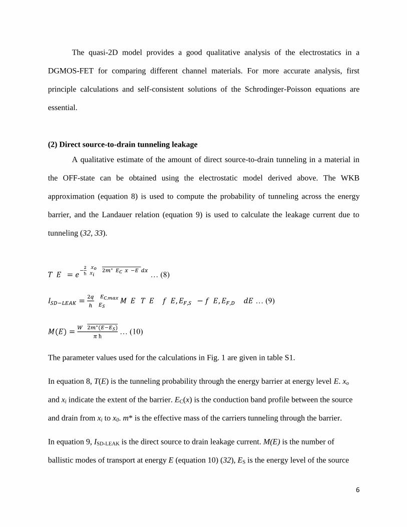
The quasi-2D model provides a good qualitative analysis of the electrostatics in a
DGMOS-FET for comparing different channel materials. For more accurate analysis, first
principle calculations and self-consistent solutions of the Schrodinger-Poisson equations are
essential.
(2) Direct source-to-drain tunneling leakage
A qualitative estimate of the amount of direct source-to-drain tunneling in a material in
the OFF-state can be obtained using the electrostatic model derived above. The WKB
approximation (equation 8) is used to compute the probability of tunneling across the energy
barrier, and the Landauer relation (equation 9) is used to calculate the leakage current due to
tunneling (32, 33).
… (8)
… (9)
… (10)
The parameter values used for the calculations in Fig. 1 are given in table S1.
In equation 8, T(E) is the tunneling probability through the energy barrier at energy level E. xo
and xi indicate the extent of the barrier. EC(x) is the conduction band profile between the source
and drain from xi to x0. m* is the effective mass of the carriers tunneling through the barrier.
In equation 9, ISD-LEAK is the direct source to drain leakage current. M(E) is the number of
ballistic modes of transport at energy E (equation 10) (32), ES is the energy level of the source

7
(reference) and EC,max is the top of the conduction band profile between the source and drain. f(E)
is the Fermi-Dirac distribution and EF,S and EF,D are the Fermi levels in source and drain
respectively.
TMDCs have a higher effective mass along the direction of transport (e.g. ~ 0.55 for
MoS2 versus ~ 0.19 for Si [100]) (19, 34) which reduces the tunneling probability and
therefore ISD-LEAK. Figure 1 discusses the impact of effective mass on transistor scaling using the
example of a symmetric double-gate MOSFET (DGMOS-FET) structure (Fig. S1). Figure 1A
shows normalized ISD-LEAK as a function of channel thickness for Si and MoS2. The channel
conduction band profile required to calculate ISD-LEAK is derived using the analytical 2D
DGMOS-FET electrostatic model proposed in ref (21). The parameter values used in the
calculations (table S1) account for quantum mechanical effects on the bandgap, dielectric
constant and effective mass at ultra-thin channel thicknesses (19, 35-39). MoS2 shows more than
two orders reduction in ISD-LEAK compared to Si due to the larger electron effective mass. Figure
1B plots the dependence of ISD-LEAK on LG. The dotted lines in Fig. 1A and 1B represent the Low
Operating Power (LOP) limit for the 2026 technology node as specified by the international
technology roadmap for semiconductors (ITRS) (40). Figure 1B reveals that for similar channel
thickness, MoS2 transistors can be scaled to shorter gate lengths as compared to Si.
(3) Calculation of DIT
… (11)
Equation 11 relates SS to the interface trap density for the device (41). Here k is the Boltzmann
constant, T is temperature in Kelvin and q is the charge of an electron. For the 1D2D-FET

8
structure, CD (depletion capacitance) ~ 0, CIT (interface trap capacitance) = qDIT and COX (oxide
capacitance) = εOX/TOX. εOX is the permittivity of the gate oxide (ZrO2 dielectric constant ~ 25
(42)) and TOX is the oxide thickness (~ 5.8 nm) measured from TEM in Fig. 2D.
(4) Analytical derivation of parasitic capacitance from fringing electric fields
Figure S8 shows the fringing electric field lines in an underlap transistor. The fringing electric
field lines lead to parasitic capacitance (Cparasitic) and a larger effective channel length (LEFF).
… (12)
… (13)
Equation 12 gives the capacitance COX for the parallel electric field lines from the gate electrode
to the channel. is the electric permittivity of the gate dielectric, W is the width and LG is the
physical gate length. TOX = (TZrO2 – TG) is kept constant for devices of different gate heights (TG).
Equation 13 calculates the parasitic capacitance due to the fringing electric field lines from the
gate electrode and is dependent on TG. Larger the height of the electrode, higher is the parasitic
capacitance. The natural short height of a SWCNT helps achieve small LEFF and small Cparasitic
compared to lithographically patterned tall gate structures. The above simplistic analytical
derivation for Cparasitic assumes the fringing electric field lines to be circular (Fig. S8) and
underestimates the capacitance. For accurate analysis, simulation of the 2D electrostatics in the
device is essential.

9
Figure S1: Schematic of dual-gated metal-oxide-semiconductor-field-effect-transistor.
Schematic of a symmetric dual-gated metal-oxide-semiconductor-field-effect-transistor
(DGMOS-FET) used to study impact of channel material properties on the scaling limit of
transistors in Fig. 1.
G
G
DS
x
TCH
LG
TOX
y

10
Figure S2: Dependence of characteristic length on channel thickness. Device electrostatic
characteristic length (λ) as a function of channel thickness (TCH) for Si and MoS2.
1 2 3
0.6
0.9
1.2
1.5
1.8
Si (
nm
)
TCH
(nm)
MoS2
TOX = 0.5 nm
εOX,y = 3.9 ε0

11
Figure S3: Detailed process flow for SWCNT gated MoS2 FET
B: SEM mapping of
SWCNT
SWCNT
C: Pattern Pd gate contacts to
SWCNTD: IS-VBS measurement to identify
semiconducting and metallic SWCNT
-6 -4 -2 0 2 4 610
-13
10-11
10-9
10-7
10-5
VDS
= -1 V
Semiconducting
I S (
A)
VBS
(V)
Metallic
A: SWCNT transfer process
E: AFM map of device to locate
SWCNT
F: ALD ZrO2, MoS2 transfer G: Pattern Ni source and
drain contacts to MoS2
SWCNT
SWCNT
SWCNT
SWCNT
G
G
G
G
G
G
DS
MoS2

12
Figure S3 shows the detailed process flow for the device fabrication. The first step of the process
involves the transfer of grown SWCNT from the growth substrate (quartz) to the target 50 nm
SiO2 / Si substrate using gold as the transfer layer (23) (Fig. S3A). The target substrate is pre-
patterned with 0.5/30 nm Cr/Pt alignment markers. These alignment markers are used to
relatively locate the transferred SWCNT in a scanning electron microscope (SEM) image (Fig.
S3B). Care is taken to ensure the SWCNTs are not damaged during the SEM by minimizing the
exposure time under the electron-beam. Gate electrodes are then patterned using electron-beam
lithography followed by 30 nm Pd evaporation and liftoff process (Fig. S3C). IS-VBS
measurements of the SWCNT devices help to identify the metallic or semiconducting nature of
the SWCNT (Fig. S3D). After the measurement, the SWCNT devices are mapped with an atomic
force microscope (AFM) to find the relative location of the SWCNT with respect to the gate
electrodes (Fig. S3E). Post the AFM map, ZrO2 gate dielectric is deposited using atomic layer
deposition (ALD) and the MoS2 flake is transferred on top using a dry pick and transfer method
(14) using poly(methyl methacrylate) (PMMA) as the transfer medium (Fig. S3F). The AFM
map taken prior to the ALD is then used as a mask for a second electron-beam lithography step,
to pattern the source and drain electrodes (Ni 40 nm) as shown in Fig. S3G, thus completing the
device fabrication.
13
Figure S4: EELS map. EELS mapping of the 1D2D-FET showing the spatial location of the
different elements (EDS map is shown for Mo). Carbon mapping clearly indicates the position of
the SWCNT under the ZrO2 gate dielectric and the MoS2 flake on top of it. Carbon seen on top
of the ZrO2 can be attributed to organic residue like PMMA and contaminants from processing
steps and dry transfer of MoS2.
C Si O
SZr Mo5 nm
ZrO2
SiO2
SiO2
MoS2
SWCNT
A B
14
Figure S5: ID-VBS characteristics obtained by varying the n
+ Si back gate. ID-VBS
characteristics for the device in Fig. 3A-C. The MoS2 extensions regions are completely inverted
using the Si back gate at VBS = 5 V.

15
Figure S6: Energy band diagrams in ON and OFF-states. Energy band diagrams
corresponding to the TCAD simulations in Fig. 3D-G. VBS = 5 V, VDS = 50 mV, (VGS - VT) = 1.5
V (ON) and (VGS - VT) = -0.3 V (OFF), for the 2L MoS2 device. In the OFF-state the bias applied
to the SWCNT creates a barrier which opposes the flow of carriers from source to drain. In the
ON-state no barrier exists to the flow of electrons from the source to drain and the ON-current is
limited by the series resistance of the extension regions.
ONOFFA B
-30 -20 -10 0 10 20 30
-1.6
-1.2
-0.8
-0.4
0.0
0.4
Energ
y (
eV
)
X (nm)
EV
Fn, F
p
EC
-30 -20 -10 0 10 20 30
-1.6
-1.2
-0.8
-0.4
0.0
0.4
Energ
y (
eV
)
X (nm)
EC
Fn, F
p
EV

16
Figure S7: Electron density contour plots. Dependence of LEFF on the definition of OFF-state
and nthershold (electron density below which the channel is considered depleted) for VBS = 5 V, VDS
= 50 mV (27-29). The OFF-state corresponds to (VGS - VT) = -0.3 V and ON-state corresponds to
(VGS - VT) = 1.5 V (or an ON/OFF current ratio of ~ 106). LEFF is of the order of 5 nm as seen
from the simulations. The 2D electron density is obtained by multiplying the 3D density obtained
from simulations with TCH, by assuming uniform distribution along the thickness of MoS2.
e- density (cm-2)
6.5 x 10¹²
2.1 x 10⁹
1.3 x 10⁵
LEFF ~ 3.9 nm
SiO2
ZrO2
MoS2 OFF
4 nm
SWCNT
e- density (cm-2)
6.5 x 10¹²
2.1 x 10⁹
6.5 x 10⁵
LEFF ~ 8.4 nm
SiO2
ZrO2
MoS2 OFF
4 nm
SWCNT
A: (VGS-VT) = -0.3 V, nthreshold = 1.3 105 cm-2
B: (VGS-VT) = -0.3 V, nthreshold = 6.5 105 cm-2

17
Figure S8: Parasitic capacitance and dependence on gate height. Effective channel length
(LEFF) > physical gate length (LG) due to fringing electric field. LEFF and Cparasitic increase as the
height of the gate (TG) increases, for the same value of TOX (TZrO2 – TG). LEFF and Cparasitic are
small for a SWCNT gate as compared to lithographically defined gates because of the naturally
short height of a SWCNT, and hence less fringing electric field lines coupling to the channel
(43).
SiO2
MoS2
S D
ZrO2
LEFF > LG
LG
TZrO2
TG
COX CparasiticCparasitic

18
Figure S9: Dependence of DIBL on gate oxide thickness. Drain-induced barrier-lowering
(DIBL) as a function of the ZrO2 thickness calculated using simulations. Effective oxide
thickness (EOT) scaling helps improve the electrostatics in the device and reduce DIBL.
2 3 4 5 6 7 80
20
40
60
80
100
120
140
DIB
L (
mV
/V)
TOX
(nm)
VBS = 5 V

19
Figure S10: Thickness dependence of MoS2. IDS-VGS curves for several different channel
thicknesses from TCAD simulations used to calculate SS in Fig. 4B. The TCAD results
qualitatively match the experimental trends. Doping of MoS2 (ND) is assumed to be 1017
cm-3
,
and the dielectric constant of ZrO2 = 25 (42). Electron affinity of MoS2 is assumed to be 4 eV
(44). All other values are as specified in table S1. For more quantitative comparison, the analysis
must involve simulation of the 2D density of states for MoS2, correction for contact resistance,
oxide and interface traps, along with using more accurate values for m*, EG, ND, etc.

20
Table S1: Parameter values used for calculations in Fig. 1 and Fig. S2. Values have been
extracted from references (19, 35-39). The effects of quantum confinement at atomic-scale
channel thicknesses on parameter values like bandgap, dielectric constant and effective mass are
considered for more accurate analysis. The bandgap values for MoS2 correspond to the optical
bandgap from photoluminescence spectra. The bandgap of Si is obtained from optical absorption
spectra.
MoS2 Si
TCH
(nm) ε (relative) (35) EG
(38) me* (19) T
CH (nm) ε (relative) (36) E
G (37) m
e* (39)
0.65 3.93 1.88 ~ 0.55 0.5431 4.39
~ 0.22
1.3 4.71 1.59 ~ 0.55 1.0862 6.62 1.90 ~ 0.22
1.95 4.90 1.47 ~ 0.55 1.6293 7.66 1.46 ~ 0.22
2.6 6.24 1.44 ~ 0.55 2.1724 8.70 1.31 ~ 0.22
3.25 7.71 1.42 ~ 0.55 2.7155 9.73 1.23 ~ 0.22
10.4 ~ 10 ~ 1.3 ~ 0.55 3.2586 10.32 1.19 ~ 0.22
31.2 ~ 10.5 ~ 1.3 ~ 0.55

21
References 1. T. N. Theis, P. M. Solomon, It’s time to reinvent the transistor! Science 327, 1600–1601
(2010). Medline doi:10.1126/science.1187597
2. R. Chau, B. Doyle, S. Datta, J. Kavalieros, K. Zhang, Integrated nanoelectronics for the future. Nat. Mater. 6, 810–812 (2007). Medline doi:10.1038/nmat2014
3. A. D. Franklin, Nanomaterials in transistors: From high-performance to thin-film applications. Science 349, aab2750 (2015). Medline doi:10.1126/science.aab2750
4. M. Lundstrom, Moore’s law forever? Science 299, 210–211 (2003). Medline doi:10.1126/science.1079567
5. M. Luisier, M. Lundstrom, D. A. Antoniadis, J. Bokor, in Electron Devices Meeting (IEDM), 2011 IEEE International (IEEE, 2011), pp. 11.12.11–1.12.14.
6. H. Kawaura, T. Sakamoto, T. Baba, Observation of source-to-drain direct tunneling current in 8 nm gate electrically variable shallow junction metal–oxide–semiconductor field-effect transistors. Appl. Phys. Lett. 76, 3810–3812 (2000). doi:10.1063/1.126789
7. W. S. Cho, K. Roy, The effects of direct source-to-drain tunneling and variation in the body thickness on (100) and (110) sub-10-nm Si double-gate transistors. IEEE Electron Device Lett. 36, 427–429 (2015). doi:10.1109/LED.2015.2413785
8. B. Radisavljevic, A. Radenovic, J. Brivio, V. Giacometti, A. Kis, Single-layer MoS2 transistors. Nat. Nanotechnol. 6, 147–150 (2011). Medline doi:10.1038/nnano.2010.279
9. D. Sarkar, X. Xie, W. Liu, W. Cao, J. Kang, Y. Gong, S. Kraemer, P. M. Ajayan, K. Banerjee, A subthermionic tunnel field-effect transistor with an atomically thin channel. Nature 526, 91–95 (2015). Medline doi:10.1038/nature15387
10. H. Liu, A. T. Neal, P. D. Ye, Channel length scaling of MoS2 MOSFETs. ACS Nano 6, 8563–8569 (2012). Medline doi:10.1021/nn303513c
11. H. Wang, L. Yu, Y.-H. Lee, Y. Shi, A. Hsu, M. L. Chin, L.-J. Li, M. Dubey, J. Kong, T. Palacios, Integrated circuits based on bilayer MoS₂ transistors. Nano Lett. 12, 4674–4680 (2012). Medline doi:10.1021/nl302015v
12. K. F. Mak, K. L. McGill, J. Park, P. L. McEuen, The valley Hall effect in MoS₂ transistors. Science 344, 1489–1492 (2014). Medline doi:10.1126/science.1250140
13. D. Jariwala, V. K. Sangwan, L. J. Lauhon, T. J. Marks, M. C. Hersam, Emerging device applications for semiconducting two-dimensional transition metal dichalcogenides. ACS Nano 8, 1102–1120 (2014). Medline doi:10.1021/nn500064s
14. H. Fang, C. Battaglia, C. Carraro, S. Nemsak, B. Ozdol, J. S. Kang, H. A. Bechtel, S. B. Desai, F. Kronast, A. A. Unal, G. Conti, C. Conlon, G. K. Palsson, M. C. Martin, A. M. Minor, C. S. Fadley, E. Yablonovitch, R. Maboudian, A. Javey, Strong interlayer coupling in van der Waals heterostructures built from single-layer chalcogenides. Proc. Natl. Acad. Sci. U.S.A. 111, 6198–6202 (2014). Medline doi:10.1073/pnas.1405435111
15. K. S. Novoselov, D. Jiang, F. Schedin, T. J. Booth, V. V. Khotkevich, S. V. Morozov, A. K. Geim, Two-dimensional atomic crystals. Proc. Natl. Acad. Sci. U.S.A. 102, 10451–10453 (2005). Medline doi:10.1073/pnas.0502848102
22
16. C.-H. Lee, G.-H. Lee, A. M. van der Zande, W. Chen, Y. Li, M. Han, X. Cui, G. Arefe, C. Nuckolls, T. F. Heinz, J. Guo, J. Hone, P. Kim, Atomically thin p-n junctions with van der Waals heterointerfaces. Nat. Nanotechnol. 9, 676–681 (2014). Medline doi:10.1038/nnano.2014.150
17. Y. Yoon, K. Ganapathi, S. Salahuddin, How good can monolayer MoS₂ transistors be? Nano Lett. 11, 3768–3773 (2011). Medline doi:10.1021/nl2018178
18. L. Liu, Y. Lu, J. Guo, On Monolayer MoS2 field-effect transistors at the scaling limit. IEEE Trans. Electron. Dev. 60, 4133–4139 (2013). doi:10.1109/TED.2013.2284591
19. D. Wickramaratne, F. Zahid, R. K. Lake, Electronic and thermoelectric properties of few-layer transition metal dichalcogenides. J. Chem. Phys. 140, 124710 (2014). Medline doi:10.1063/1.4869142
20. Supplementary materials are available on Science Online.
21. K. Suzuki, T. Tanaka, Y. Tosaka, H. Horie, Y. Arimoto, Scaling theory for double-gate SOI MOSFET's. IEEE Trans. Electron. Dev. 40, 2326–2329 (1993). doi:10.1109/16.249482
22. J. Svensson, Y. Tarakanov, D. S. Lee, J. M. Kinaret, Y. W. Park, E. E. B. Campbell, A carbon nanotube gated carbon nanotube transistor with 5 ps gate delay. Nanotechnology 19, 325201 (2008). Medline doi:10.1088/0957-4484/19/32/325201
23. N. Patil, A. Lin, E. R. Myers, K. Ryu, A. Badmaev, C. Zhou, H.-S. P. Wong, S. Mitra, wafer-scale growth and transfer of aligned single-walled carbon nanotubes. IEEE Trans. NanoTechnol. 8, 498–504 (2009). doi:10.1109/TNANO.2009.2016562
24. J.-P. Colinge, C.-W. Lee, A. Afzalian, N. D. Akhavan, R. Yan, I. Ferain, P. Razavi, B. O’Neill, A. Blake, M. White, A.-M. Kelleher, B. McCarthy, R. Murphy, Nanowire transistors without junctions. Nat. Nanotechnol. 5, 225–229 (2010). Medline doi:10.1038/nnano.2010.15
25. A. Javey, J. Guo, D. B. Farmer, Q. Wang, E. Yenilmez, R. G. Gordon, M. Lundstrom, H. Dai, Self-aligned ballistic molecular transistors and electrically parallel nanotube arrays. Nano Lett. 4, 1319–1322 (2004). doi:10.1021/nl049222b
26. X. Zou, J. Wang, C.-H. Chiu, Y. Wu, X. Xiao, C. Jiang, W.-W. Wu, L. Mai, T. Chen, J. Li, J. C. Ho, L. Liao, Interface engineering for high-performance top-gated MoS2 field-effect transistors. Adv. Mater. 26, 6255–6261 (2014). Medline doi:10.1002/adma.201402008
27. Y. Taur, MOSFET channel length: Extraction and interpretation. IEEE Trans. Electron. Dev. 47, 160–170 (2000). doi:10.1109/16.817582
28. L. Barbut, F. Jazaeri, D. Bouvet, J.-M. Sallese, Downscaling and short channel effects in twin gate junctionless vertical slit FETs. Int. J. Microelectron. Comput. Sci. 4, 103–109 (2013).
29. S. Hong, K. Lee, Extraction of metallurgical effective channel length in LDD MOSFET's. IEEE Trans. Electron. Dev. 42, 1461–1466 (1995). doi:10.1109/16.398660
30. K. Kang, S. Xie, L. Huang, Y. Han, P. Y. Huang, K. F. Mak, C.-J. Kim, D. Muller, J. Park, High-mobility three-atom-thick semiconducting films with wafer-scale homogeneity. Nature 520, 656–660 (2015). Medline doi:10.1038/nature14417

23
31. D. J. Frank, Y. Taur, H. S. P. Wong, Generalized scale length for two-dimensional effects in MOSFETs. IEEE Electron Device Lett. 19, 385–387 (1998). doi:10.1109/55.720194
32. Mark Lundstrom, (2005), “Notes on the Ballistic MOSFET,” https://nanohub.org/resources/489.
33. C. S. Lee, E. Pop, A. D. Franklin, W. Haensch, H. S. P. Wong, A compact virtual-source model for carbon nanotube FETs in the sub-10-nm regime–Part II: Extrinsic elements, performance assessment, and design optimization. IEEE Trans. Electron. Dev. 62, 3070–3078 (2015). doi:10.1109/TED.2015.2457424
34. H. D. Barber, Effective mass and intrinsic concentration in silicon. Solid-State Electron. 10, 1039–1051 (1967). doi:10.1016/0038-1101(67)90122-0
35. X. Chen, Z. Wu, S. Xu, L. Wang, R. Huang, Y. Han, W. Ye, W. Xiong, T. Han, G. Long, Y. Wang, Y. He, Y. Cai, P. Sheng, N. Wang, Probing the electron states and metal-insulator transition mechanisms in molybdenum disulphide vertical heterostructures. Nat. Commun. 6, 6088 (2015). Medline doi:10.1038/ncomms7088
36. G. Zhang, M. B. Yu, C. H. Tung, G. Q. Lo, Quantum size effects on dielectric constants and optical absorption of ultrathin silicon films. IEEE Electron Device Lett. 29, 1302–1305 (2008). doi:10.1109/LED.2008.2005651
37. H. Jang, W. Lee, S. M. Won, S. Y. Ryu, D. Lee, J. B. Koo, S.-D. Ahn, C.-W. Yang, M.-H. Jo, J. H. Cho, J. A. Rogers, J.-H. Ahn, Quantum confinement effects in transferrable silicon nanomembranes and their applications on unusual substrates. Nano Lett. 13, 5600–5607 (2013). Medline doi:10.1021/nl403251e
38. K. F. Mak, C. Lee, J. Hone, J. Shan, T. F. Heinz, Atomically thin MoS₂: A new direct-gap semiconductor. Phys. Rev. Lett. 105, 136805 (2010). Medline doi:10.1103/PhysRevLett.105.136805
39. Y. Liu, N. Neophytou, T. Low, G. Klimeck, M. S. Lundstrom, A tight-binding study of the ballistic injection velocity for ultrathin-body SOI MOSFETs. IEEE Trans. Electron. Dev. 55, 866–871 (2008). doi:10.1109/TED.2007.915056
40. International Technology Roadmap for Semiconductors (ITRS) 2013, http://www.itrs2.net/2013-itrs.html.
41. S. M. Sze, K. K. Ng, Physics of Semiconductor Devices (3rd ed., Wiley, 2006).
42. P. Harrop, J. Wanklyn, The dielectric constant of zirconia. Br. J. Appl. Phys. 18, 739–742 (1967). doi:10.1088/0508-3443/18/6/305
43. H. Zhao, Y. C. Yeo, S. C. Rustagi, G. S. Samudra, Analysis of the effects of fringing electric field on FinFET device performance and structural optimization using 3-D simulation. IEEE Trans. Electron. Dev. 55, 1177–1184 (2008). doi:10.1109/TED.2008.919308
44. S. Das, H.-Y. Chen, A. V. Penumatcha, J. Appenzeller, High performance multilayer MoS2 transistors with scandium contacts. Nano Lett. 13, 100–105 (2013). Medline doi:10.1021/nl303583v