Embed Size (px)
Citation preview

Intrinsic Optoelectronic Characteristics ofMoS2 Phototransistors via a Fully Transparentvan der Waals HeterostructureJinsu Pak,† Ilmin Lee,‡ Kyungjune Cho,† Jae-Keun Kim,† Hyunhak Jeong,† Wang-Taek Hwang,†
Geun Ho Ahn,# Keehoon Kang,† Woo Jong Yu,‡,§ Ali Javey,# Seungjun Chung,*,⊥
and Takhee Lee*,†
†Department of Physics and Astronomy, and Institute of Applied Physics, Seoul National University, Seoul 08826, Korea‡Department of Electrical and Computer Engineering, Sungkyunkwan University, Suwon 16419, Korea#Electrical Engineering and Computer Sciences, University of California, Berkeley, California 94720, United States§Center for Integrated Nanostructure Physics, Institute for Basic Science (IBS), Suwon 16419, Republic of Korea⊥Photo-Electronic Hybrids Research Center, Korea Institute of Science and Technology (KIST), Seoul 02792, Korea
*S Supporting Information
ABSTRACT: In the past decade, intensive studies onmonolayer MoS2-based phototransistors have been carriedout to achieve further enhanced optoelectronic character-istics. However, the intrinsic optoelectronic characteristicsof monolayer MoS2 have still not been explored until nowbecause of unintended interferences, such as multiplereflections of incident light originating from commonlyused opaque substrates. This leads to overestimatedphotoresponsive characteristics inevitably due to theenhanced photogating and photoconductive effects. Here,we reveal the intrinsic photoresponsive characteristics ofmonolayer MoS2, including its internal responsivity and quantum efficiency, in fully transparent monolayer MoS2phototransistors employing a van der Waals heterostructure. Interestingly, as opposed to the previous reports, the internalphotoresponsive characteristics do not significantly depend on the wavelength of the incident light as long as theelectron−hole pairs are generated in the same k-space. This study provides a deeper understanding of thephotoresponsive characteristics of MoS2 and lays the foundation for two-dimensional materials-based transparentphototransistors.KEYWORDS: MoS2, phototransistor, heterostructure, internal quantum efficiency, internal responsivity
Beginning with extensive research on graphene, theemergence of atomically thin two-dimensional (2D)materials has attracted substantial attention in the
fundamental scientific studies and the next generation ofelectronics.1−4 In this group of 2D materials, especiallymolybdenum disulfide (MoS2) has been extensively studiedas a promising candidate for realizing 2D materials-basedflexible photodetectors due to its outstanding optoelectronicproperties, such as intrinsic bandgap, high photodetectioncapability, high carrier mobility, good electrical stability, andmechanical flexibility.5−10 Recently, MoS2-based 2D hetero-structures have been designed to enhance photodetection andphotoswitching abilities, which is attributed to the high-qualityinterfacial properties between 2D materials held together bythe weak van der Waals (vdW) interaction without covalentbonds. For instance, vdW heterostructured MoS2 photodiodes
made with tungsten diselenide (WSe2), molybdenum ditellur-ide (MoTe2), and black phosphorus have been realized toimprove photoresponsive characteristics.11−15 Also, MoS2phototransistors with hexagonal boron nitride (h-BN),graphene, and tin diselenide (SnSe2) in a vertical vdWheterostructure have shown enhanced responsivity or fasterphotoswitching behaviors.16−18 Although numerous results ofthe optoelectronic properties of vdW heterostructured photo-detectors have been reported, to date, the intrinsicoptoelectronic characteristics of atomically thin MoS2 havenot been explored because most previous studies haveemployed opaque substrates, typically heavily doped Si with
Received: June 19, 2019Accepted: July 25, 2019Published: July 25, 2019
Artic
lewww.acsnano.orgCite This: ACS Nano XXXX, XXX, XXX−XXX
© XXXX American Chemical Society A DOI: 10.1021/acsnano.9b04829ACS Nano XXXX, XXX, XXX−XXX
Dow
nloa
ded
via
UN
IV O
F C
AL
IFO
RN
IA B
ER
KE
LE
Y o
n A
ugus
t 14,
201
9 at
16:
03:1
5 (U
TC
).Se
e ht
tps:
//pub
s.ac
s.or
g/sh
arin
ggui
delin
es f
or o
ptio
ns o
n ho
w to
legi
timat
ely
shar
e pu
blis
hed
artic
les.

SiO2, due to the convenience from a manufacturingperspective. The opaque platforms allow multiple reflectionsof incident light, which results in the generation of additionalelectron−hole pairs at the MoS2/SiO2 and SiO2/Si inter-faces.19 Furthermore, this unintended interference causes astrong photogating effect due to the trapping of photo-generated holes at the low-quality interface,20,21 which canoverestimate the ability of the photoresponsivity of MoS2. Fora better understanding of MoS2, in this regard, the systematicinvestigation of the intrinsic optoelectronic characteristics ofmonolayer MoS2 is highly desirable without effects caused byexternal interference such as reflected or refractive light.Here, we report the intrinsic optoelectronic characteristics of
monolayer MoS2 phototransistors via a fully transparent vdWheterostructure with h-BN (as a dielectric layer) and graphene(as a gate electrode). The 2D h-BN dielectric provided a near-ideal interface with MoS2 enabling low-voltage operation. Toinvestigate the intrinsic photoresponsive properties of MoS2,we compared the characteristics of the MoS2 phototransistorsfabricated on transparent polyethylene naphthalate (PEN) andopaque SiO2/Si substrates. From the results, it turned out thatthe MoS2 phototransistors fabricated on the opaque SiO2/Sisubstrate showed higher photoresponsive performances due tothe enhanced photogating and photoconductive effects causedby multiple reflections of the incident light. From the MoS2phototransistors fabricated on the transparent PEN substrate,the intrinsic photoresponsive properties were revealed;specifically, an internal responsivity of 3.2 × 10² A/W andinternal quantum efficiency (IQE) of 7.1 × 10⁵ % wereachieved. Interestingly, unlike the external photoresponsedetermined by the incident photons that shows wavelength-dependent characteristics, the internal photoresponse deter-mined by absorbed photons in the MoS2 channel did notsignificantly depend on the wavelength of the incident light.Furthermore, we found that the intrinsic photoresponsive
characteristics of MoS2 could be dependent on the locationswhere photogeneration occurred in k-space and the conse-quent alteration of the effective mass.
RESULTS AND DISCUSSION
For the realization of transparent MoS2 phototransistors,ready-made MoS2 field-effect transistors (FETs) on a SiO2/Sisubstrate were transferred to a PEN substrate via the transfermethod using potassium hydroxide etching solution (seeMethods and Figure S1 in the Supporting Information formore details of the fabrication process). To enhance thereproducibility of MoS2 phototransistors, chemical vapordeposition (CVD)-grown monolayer MoS2 was used as achannel layer in 2D vdW heterostructured FETs. In addition,by employing CVD-grown monolayer graphene as a gateelectrode and mechanically exfoliated multilayer h-BN (41 nmthick) as a gate dielectric on a transparent PEN substrate (125μm thick), good transparency of over 80% in the visible rangewas achieved. Figure 1a shows a schematic illustrating thevertically stacked vdW heterostructure on a PEN substrate.After the realization of the 2D heterostructure using amicromanipulator system (AP-4200GP, UNITEK), no drasti-cally degraded transparency was observed in the optical image(Figure 1b). The Raman frequency difference (20 cm−1)(upper panel, Figure 1c) and a photoluminescence (PL)mapping image displaying uniform bandgap energy (1.86 eV)(Figure 1d) support the fact that the CVD-grown MoS2 usedfor the channel was a uniform monolayer.22 In addition, theRaman peak observed for the multilayer h-BN at 1364 cm−1 isassigned to the in-plane vibration (E2g mode).23 The largeintensity of the 2D-band relative to the G-band, which can onlybe observed in monolayer graphene due to a triple-resonanceprocess, shows that monolayer graphene film was well grownvia the optimized CVD process (lower panel, Figure 1c).24 All
Figure 1. (a) Schematic of the vdW heterostructure on a PEN substrate. (b) Optical image of a fabricated fully transparent MoS2phototransistor. (c) Raman spectra for the CVD-grown monolayer MoS2 and graphene (denoted as Gr) and mechanically exfoliatedmultilayer h-BN. Scale bar = 5 μm. (d) PL mapping image with a 1.86 eV peak intensity. Scale bar = 5 μm. (e) IDS−VGS and (f) IDS−VDScurves for the fully transparent MoS2 phototransistor. (g) Logarithmic scale plot for IDS−VDS with an average γ value of 1.01.
ACS Nano Article
DOI: 10.1021/acsnano.9b04829ACS Nano XXXX, XXX, XXX−XXX
B

Raman spectra in Figure 1c were measured before transfer to aPEN substrate for observing the distinct spectrum.Figure 1e and f show the transfer curve (drain−source
current versus gate voltage, IDS−VGS) and the output curve(drain−source current versus drain voltage, IDS−VDS) for thetransparent CVD-grown monolayer MoS2 FET measuredunder vacuum (∼10−4 Torr) at room temperature. Arisingfrom the thin h-BN dielectric layer, a low operation voltageranging from −4 to 5 V was achieved. The maximum field-effect mobility (μ) was determined to be 12.2 cm2/V·s(extracted at VGS = 5 V and VDS = 0.25 V), as calculated usingthe formula
ikjjjjj
y{zzzzz
IV
LWC V
1
i
DS
GS DSμ =
∂∂ (1)
with a channel width W = 8.56 μm, channel length L = 5.05μm, and unit capacitance for the h-BN dielectric Ci = 0.756mF/cm2 (thickness of 41 nm and dielectric constant of 3.5 forh-BN were considered25,26). VGS-dependent mobilities27 atdifferent VDS are indicated in Figure S2 in the SupportingInformation. Figure 1g shows the logarithmic scale plot forIDS−VDS measured at VGS ranging from 0 to 5 V. The extractedaverage γ (linearity parameter in the output curve) value of1.01 in the output characteristics indicates ohmic contactsbetween the MoS2 channel layer and Au electrodes.Figure 2a shows the transmittance and reflectance of the
device on stacking the individual layers: transparent substrate(PEN), CVD-grown monolayer graphene (denoted as Gr)/PEN, h-BN/Gr/PEN, and CVD-grown monolayer MoS2/h-BN/Gr/PEN. Negligible absorption in the visible range for Grand multilayer h-BN was verified through the observation ofunchanged transmittance values after stacking the Gr and h-BNlayers onto a PEN substrate. The absorbance of CVD-grownmonolayer MoS2 was determined by subtracting thereflectance of the MoS2 layer from the diminished trans-mittance after stacking the MoS2 layer onto an underlying h-BN/Gr/PEN layer (Figure 2b). The extracted absorbance ofthe MoS2 layer was used as a reference to investigate the
internal optoelectronic characteristics by absorbed photons,not incident photons in the MoS2 channel. In Figure 2b, theresonance peaks A and B correspond to excitonic transitionssplit by spin−orbit coupling at the K point in k-space.22,28 Thestrong resonance peak C is ascribed to the parallel bands in thedensity of states even for excitation energy far exceeding thebandgap of MoS2; this is called the band-nesting effect, whichleads to a divergence in the joint density of states.29,30 Byemploying transparent layers of Gr, MoS2, h-BN, and PEN,fully transparent MoS2 phototransistors were implementedwith high transparency, as shown in Figure 2c. Also, theincident laser light fully penetrated through the fully stackedMoS2 phototransistors without reflection or dispersion (right,Figure 2c).To investigate the effects of the unintended photoresponsive
characteristics, which are attributed to the use of an opaquesubstrate, CVD-grown monolayer MoS2 phototransistors werefabricated with a h-BN dielectric on both a transparent PENsubstrate (MoS2/h-BN/Gr, denoted as MhG) and an opaque100 nm thick SiO2/Si substrate (MoS2/h-BN/heavily dopedsilicon, denoted as MhS), as depicted in Figure 3a and b,respectively. The photoresponsive characteristics for MhG andMhS were investigated under various illumination conditionswith different light intensities ranging from 15 to 1180 nW at afixed wavelength of 450 nm and with different wavelengthsranging from 780 to 450 nm at a fixed light intensity of 3 μWin ambient air at room temperature (Figure 3c−f). Note thatthe diameter of the laser spot was ∼1 μm, smaller than thechannel area dimension, so that the entire laser light wasfocused within the MoS2 channel area. As shown in Figure 3c−f, the photoinduced current steadily increased in both types ofdevices, MhG and MhS, as the illumination intensity becamestronger at a fixed wavelength (Figure 3c and e) and also as thewavelength of the incident light became shorter at a fixedillumination intensity (Figure 3d and f). As shown in Figure 3dand f, the electron−hole pairs could be created by illuminationwith laser photon energy (1.59 and 1.80 eV, corresponding to780 and 688 nm, respectively) smaller than the optical
Figure 2. (a) Transmittances (solid lines) and reflectances (dashed lines) corresponding to each heterostructure. (b) Absorbance of theCVD-grown monolayer MoS2 indicating three resonance peaks: A, B, and C. (c) Photographic images displaying high transparency.
ACS Nano Article
DOI: 10.1021/acsnano.9b04829ACS Nano XXXX, XXX, XXX−XXX
C
bandgap energy of MoS2 (1.9 eV)31 via the excitation ofcarriers localized in band tail states. For a more accuratecomparison, the gate electric field (EGS) instead of VGS wasused as the x-axis in Figure 3c−f because of the differentthicknesses of the dielectric layers in MhG and MhS. Note thatthe contour plots visualizing the photoresponsive character-istics of MhG and MhS are indicated in Figure S4 in theSupporting Information. There were two noticeable distinc-tions in the photoresponsive characteristics for MhG and MhS:(1) the amount of change in the threshold electric field(ΔETH) in MhS due to illumination was larger than that inMhG (Figure 3g), and (2) the responsivity (R) of MhS washigher than that of MhG (Figure 3h). To understand thedifference in the photoresponsive properties between MhGand MhS, the components of the photoinduced current shouldbe classified.To date, various mechanisms for the photoinduced current
in MoS2 have been proposed, such as the photoelectric (PE),photothermoelectric (PTE), photogating (PG), and photo-conductive (PC) effects. Typically, the PE and PTE effectsdominate in the photoresponse in cases without an electricfield; therefore, the PG and PC effects dominantly determinethe photoconductivity in phototransistors when an electricfield is applied.20 The PG effect is attributed to structuraldefects in MoS2 itself or to disorder caused by the imperfectinterface between MoS2 and substrate at which the photo-generated electrons or holes can be trapped, playing the role of
a local gate electric field. In addition, trapped charges in thedielectric layer itself can also contribute to the photogatingeffect. In n-type MoS2-based FETs, a negative shift in thethreshold voltage (VTH) is typically observed due to the PGeffect via the trapped photogenerated holes.20 In contrast, thePC effect corresponds to the contribution of increased channelcurrent due to the photogenerated carriers in the channel,which influence VTH less. So, the total photocurrent (IPh) canbe expressed as
ikjjj
y{zzzI I I g V
WL
VPh Ph,PG Ph,PC m TH DS σ= + = |Δ | + Δ(2)
where g IVm
dd
DS
GS= is the transconductance and Δσ = qμnΔn is
the change in conductivity due to the photogenerated carriers.Although the proportion between the PG and PC effects differsdepending on the device structure, typically, the PG effect ismore dominant in vdW materials.20 If photogeneratedminority carriers are trapped with long lifetime depending onthe nature of the trap state, they can produce an additional gateelectric field until they disappear through recombination.32,33
When the majority carriers pass through the channel forcontributing to the photocurrent, additional majority carriersshould be injected into the channel to preserve chargeneutrality until the trapped photogenerated holes disap-pear.32,33 Therefore, the photoresponsive characteristics invdW materials-based phototransistors can be amplified by
Figure 3. Schematics for (a) MhG and (b) MhS. The thickness for the multilayer h-BN was 41 and 28 nm for MhG and MhS, respectively.The range of EGS (0.6 MV/cm) corresponds to an applied VGS of 2.46 and 7.68 V for MhG and MhS, respectively. (c−f) Photoresponsivecharacteristics of MhG and MhS under various illumination conditions with light intensity ranging from 15 to 1180 nW at a fixed wavelengthof 450 nm and wavelength ranging from 780 to 450 nm at a fixed intensity of 3 μW. (g) ETH variation versus illumination intensity and (h)wavelength-dependent responsivity of MhG and MhS at a fixed VDS of 0.5 V and EGS of 0 MV/cm. The inset figure indicates the responsivityas a function of illumination intensity at a fixed EGS of 0.5 MV/cm.
ACS Nano Article
DOI: 10.1021/acsnano.9b04829ACS Nano XXXX, XXX, XXX−XXX
D
trapping photogenerated minority carriers as well as by appliedelectric fields for accelerating the movement of the majoritycarriers.In this regard, the higher value of |ΔETH| for MhS in the low
illumination intensity regime than that for MhG (blue area inFigure 3g) indicates that the PG effect in MhS was strongerthan that in MhG in the low illumination intensity regime.This behavior is due to the influence of the reflected light fromthe SiO2/Si substrate along with the PG effect. The reflectancespectra of the device fabricated on the SiO2/Si substrate areprovided in Figure S5 in the Supporting Information. In ourstudy, the PG effect arises dominantly from the trapped holesat the intrinsic defects such as sulfur vacancies in MoS2,
34 butnot at the interface trap sites because the underlying inserted h-BN layer provided a near-ideal interface with MoS2. Therefore,the reflected light from the SiO2/Si substrate in MhS cangenerate more trapped photogenerated holes, which leads tothe enhanced PG effect in MhS in the low illuminationintensity regime. However, in the high illumination intensityregime, most trap sites can be occupied by sufficientphotogenerated holes in both MhS and MhG. Thus, thevalues for |ΔETH| for MhS and MhG became comparable in thehigh illumination intensity regime (red area in Figure 3g).Figure 3h shows the responsivity for MhS and MhG as a
function of wavelength measured at a fixed VDS of 0.5 V, EGS of0 MV/cm, and illumination intensity (P) of 3 μW. Note thatthe maximum power for the illumination intensity wasrestricted up to 3 μW to prevent any undesirable physicaldamage to the atomically thin monolayer MoS2 channel. Theresponsivity (R) is an important parameter for evaluating theperformance for photodetector applications, which is definedas
RIP
Ph
Inc=
(3)
where PInc is the incident illumination intensity. We observed ahigher responsivity for MhS than that for MhG under variouswavelengths ranging from 780 to 450 nm at a fixed intensity of3 μW, as shown in Figure 3h. This result is also attributed tothe light reflected from the SiO2/Si substrate along with thePC effect. Because the PG effects in MhS and MhG arecomparable under high-intensity illumination, the reason forthe higher responsivity of MhS is attributed to the stronger PCeffect in MhS, which originates from additional carrier creationby the reflected light from the SiO2/Si substrate (Figure 3h). Itshould be noted that the calculated number of densities-of-state at the interface MoS2/h-BN are 3.41 × 10¹² and 3.07 ×1012 cm−2 eV−1 for the MhS and MhG, respectively (seeSection 6 in the Supporting Information).35,36 This resultsupports that the different responsivities are the effectoriginated from the opaque substrate, not from the interfacialdefects. In addition, the responsivity under the variousillumination intensities ranging from 15 to 1180 nW at afixed wavelength of 450 nm and EGS of 0.5 MV/cm is indicatedin the inset of Figure 3h. Due to the stronger PG effect in MhSin the low illumination intensity regime, a higher responsivitywas observed in MhS than in MhG; then, the responsivityvalues became comparable between MhS and MhG as theillumination intensity was increased (inset of Figure 3h). Asthe illumination intensity increased, the responsivities for bothMhS and MhG were reduced. Note that an opposite result, i.e.,enhanced responsivity with increasing intensity, can beobserved at different EGS (see Figure S6 in the SupportingInformation). These different tendencies of the responsivityversus illumination intensity are primarily determined by theapplied EGS regardless of their different device structures,because the charge carrier dynamics can be changed by thelocations of the Fermi level of MoS2 set by the applied EGS (seeFigures S7 and S8 in the Supporting Information for details).The decline of the responsivity for increasing illuminationintensity can be explained in terms of restricted trap sites. In
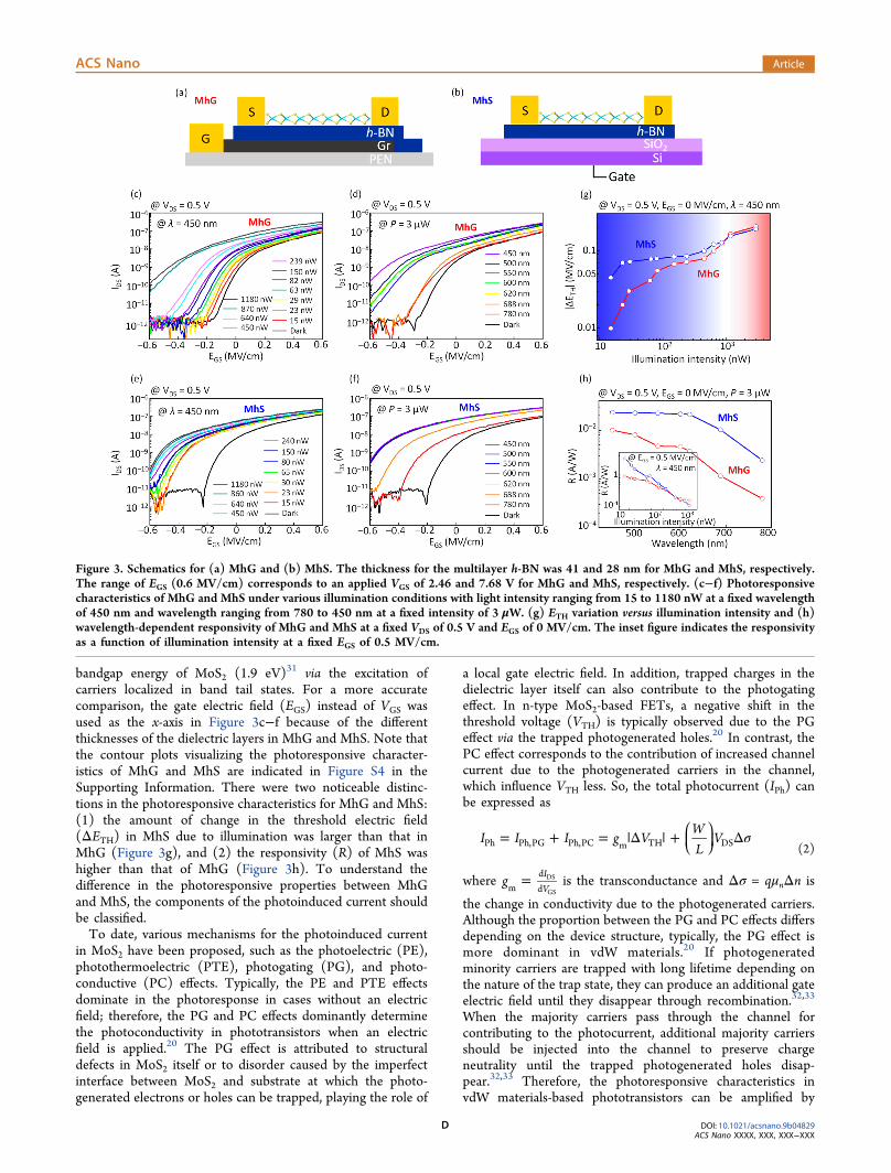
Figure 4. (a) Contour plots indicating external (upper panel) and internal (lower panel) responsivities as a function of VGS and wavelength ata fixed VDS of 0.5 V and illumination intensity of 3 μW. (b) External and internal responsivities at a fixed wavelength of 600 nm. (c) Contourplots comparing EQE (upper panel) and IQE (lower panel) at a fixed VDS of 0.5 V and illumination intensity of 3 μW. The wavelength-dependent (d) EQE and (e) IQE values (colored circle symbols) corresponding to each VGS. Absorbance for a CVD-grown MoS2 monolayeris indicated as a red solid line in (d).
ACS Nano Article
DOI: 10.1021/acsnano.9b04829ACS Nano XXXX, XXX, XXX−XXX
E
the low illumination intensity regime, a substantial portion ofthe photogenerated holes can be trapped and act as a positivegate electric field, leading to increased responsivity. On theother hand, in the high illumination intensity regime, thepossibility that the photogenerated holes can be trappedbecomes lower due to the limited number of trap sitescompared to the increased number of carriers. Therefore, theMoS2 phototransistors exhibit a higher responsivity under thelow illumination intensity.37−39 In addition, the increasedrecombination rate originating from the high density ofphotogenerated carriers can also lead to the reducedresponsivity. For these reasons, the MoS2 phototransistorsexhibit a lower responsivity under a high illumination intensity.Therefore, through a comparative analysis between MhG andMhS, it was observed that the photoresponsive characteristicsof MoS2 phototransistors fabricated on opaque substrates areoverestimated, which cannot be regarded as the intrinsicoptoelectronic characteristics of monolayer MoS2.To explore the intrinsic optoelectronic properties of MoS2,
the dependencies of the optoelectronic characteristics oftransparent MhG on VGS and wavelength were investigated(Figure 4). Note that the intrinsic optoelectronic results underthe various illumination intensities are provided in Figures S7−S9 in the Supporting Information. The contour plots indicatingexternal and internal responsivities as a function of VGS andwavelength measured at a VDS of 0.5 V are displayed in Figure4a. Because the internal responsivity value is defined as thephotocurrent per watt of the absorbed illumination intensity,the internal responsivity is calculated by dividing the external
responsivity by the absorbance of the MoS2 layer (Figure 2b)as follows:
IP
Internal responsivity Ph
Abs=
(4)
where PAbs is defined as absorbed illumination intensity (PInc =PAbs + PTr + PRef, where PTr and PRef are transmitted andreflected illumination intensities, respectively). In other words,the values for the internal responsivity are higher than those forthe external responsivity under the entire range of wavelengths(Figure 4a). To achieve the maximum responsivity inphototransistors, low illumination intensity, high VDS, andhigh VGS are required (for details, see Figure S7 in theSupporting Information). Under optimum measurementconditions, a maximum external responsivity of 16.8 A/Wand maximum internal responsivity of 3.2 × 10² A/W wereachieved (Figure S10 in the Supporting Information). Figure4c exhibits contour plots comparing the external quantumefficiency (EQE) and internal quantum efficiency (IQE) versusVGS and wavelength for a transparent MoS2 phototransistormeasured at a VDS of 0.5 V and illumination intensity of 3 μW.EQE and IQE are defined as the number of carriers detectedper incident photon and absorbed photon, respectively, asdefined by the following formula:
IP
IP
EQE (%) 100 and IQE (%) 100e
hv
e
hv
Ph/
Inc/
Ph/
Abs/= × = ×
(5)
Figure 5. (a) Photoswitching characteristics of a fully transparent MoS2 phototransistor under illumination of the MoS2 channel for 100 s atdifferent VDS conditions of 1.0 V (red open circle symbols) and 0.1 V (blue open circle symbols) at a fixed VGS of −2 V. The solid lines arelines fitted by an exponential decay function. (b) τ1 and τ2 versus VDS ranging from 0.1 to 1.0 V. (c) Photoswitching characteristics atdifferent illumination intensities of 1150 nW (red open circle symbols) and 40 nW (blue open circle symbols) at a fixed VDS of 1 V. (d) τ1and τ2 versus the illumination intensity ranging from 40 to 1150 nW.
ACS Nano Article
DOI: 10.1021/acsnano.9b04829ACS Nano XXXX, XXX, XXX−XXX
F
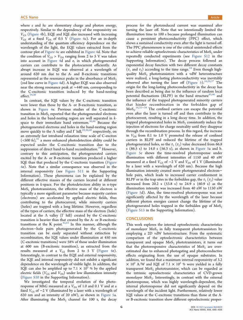
where e and hν are elementary charge and photon energy,respectively. Similar to the dependency of the responsivity onVGS (Figure 4b), EQE and IQE also increased with increasingVGS at a fixed VDS of 0.5 V (Figure 4c). For an in-depthunderstanding of the quantum efficiency dependence on thewavelength of the light, the EQE values extracted from thecontour plot of Figure 4c are exhibited in Figure 4d. Note thatthe condition of VGS > VTH ranging from 2 to 5 V was takeninto account in Figure 4d and e, in which photogeneratedcarriers can contribute to the photocurrent efficiently. Anabrupt increase in EQE was observed at a wavelength ofaround 620 nm due to the A- and B-excitonic transitionsrepresented as the resonance peaks in the absorbance of MoS2(red line curve in Figure 4d). A higher EQE was also observednear the strong resonance peak at ∼440 nm, corresponding tothe C-excitonic transition induced by the band-nestingeffect.29,30
In contrast, the IQE values by the C-excitonic transitionwere lower than those by the A- or B-excitonic transition, asshown in Figure 4e. Previous studies of the C-excitonictransition in MoS2 reported that the photogenerated electronsand holes in the band-nesting region are well separated in k-space to their immediate band extremum.30,40 Because thephotogenerated electrons and holes in the band-nesting regionmove quickly to the Λ valley and Γ hill,29,30,40 respectively, onan extremely fast intraband relaxation time scale of C-exciton(<500 fs),41 a more enhanced photodetection ability could beexpected under the C-excitonic transition due to thesuppression of direct band-to-band recombination.39 However,contrary to this anticipation, the photogenerated carriersexcited by the A- or B-excitonic transition produced a higherIQE than that produced by the C-excitonic transition (Figure4e). Note that a similar consequence was observed in theinternal responsivity (see Figure S11 in the SupportingInformation). These phenomena can be explained by thedifferent effective masses of the carriers located at differentpositions in k-space. For the photodetection ability in n-typeMoS2 phototransistors, the effective mass of the electron istypically a more significant parameter because majority carriers(electrons) are accelerated by applied electric fields, thuscontributing to the photocurrent, while minority carriers(holes) are trapped with a long lifetime. However, regardlessof the types of carriers, the effective mass of the electron (hole)located at the Λ valley (Γ hill) created by the C-excitonictransition is heavier than that created by the A- or B-excitonictransitions at the Κ point.42,43 In this manner, although theelectron−hole pairs photogenerated by the C-excitonictransition can be easily separated without extinction byrecombination, the IQE values under illumination at 450 nm(C-excitonic transitions) were 58% of those under illuminationat 600 nm (B-excitonic transition), as extracted from theresults measured at a VGS from 2 to 5 V (Figure 4e).Interestingly, in contrast to the EQE and external responsivity,the IQE and internal responsivity did not exhibit a significantdependence on the wavelength of visible light. In addition, theIQE can also be amplified up to 7.1 × 10⁵ % by the appliedelectric fields (VGS and VDS) under low illumination intensity(Figure S10 in the Supporting Information).We investigated the temporal evolution of the photo-
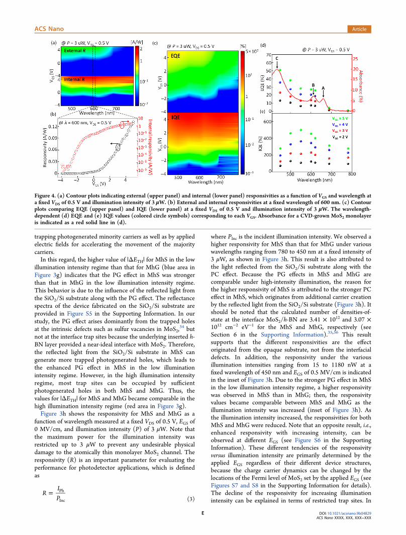
response of MhG measured at a VDS of 1.0 and 0.1 V and at afixed VGS of −2 V (illuminated by a laser with a wavelength of620 nm and an intensity of 20 nW), as shown in Figure 5a.After illuminating the MoS2 channel for 100 s, the decay
process for the photoinduced current was examined afterturning the laser off. Note that we intentionally limited theillumination time to 100 s because prolonged illumination cancause a persistent photoconductivity (PPC) effect, whichshows a sustained conductivity even after the light is turned off.The PPC phenomenon is one of the critical unintended effectsto achieve reliable optoelectronic characteristics of MoS2 underrepeatedly conducted experiments (see Figure S12 in theSupporting Information). The decay process followed anexponential decay function with two different decay constants(τ1 and τ2) according to the time range.44 Even though high-quality MoS2 phototransistors with a vdW heterostructurewere realized, a long-lasting photoconductivity was inevitablyobserved after turning the laser off (Figure 5).16,20,37 Theorigin for the long-lasting photoconductivity in the decay hasbeen described as being due to the influence of random localpotential fluctuations (RLPF) in the band structure45,46 andthe influence of the trapped photogenerated minority carriersthat hinder recombination in the forbidden gap ofMoS2.
16,32−34 The confined carriers can escape the potentialeven after the laser is turned off and then contribute to thephotocurrent, resulting in a long decay time. In addition, thetrapped photogenerated holes in MoS2 consistently induce theinjection of electrons for charge neutrality until they disappearthrough the recombination process. In this regard, the increasein VDS from 0.1 to 1.0 V promoted the release of confinedcarriers in RLPF and reduced the lifetime of the trappedphotogenerated holes, so the τ1 (τ2) value decreased from 66.8s (86.5 s) to 14.0 s (56.3 s), as shown in Figure 5a and b.Figure 5c shows the time-resolved photoresponse underillumination with different intensities of 1150 and 40 nWmeasured at a fixed VGS of −2 V and VDS of 1 V (illuminatedby a laser with a wavelength of 620 nm). Because the highillumination intensity created more photogenerated electron−hole pairs, which leads to increased carrier confinement inRLPF or in the trap sites in the forbidden gap, the τ1 (τ2) valueincreased from 20.2 s (53.8 s) to 24.9 s (60.9 s) as theillumination intensity was increased from 40 nW to 1150 nW(Figure 5d). Also, the time-resolved photoresponse was notsignificantly affected by the wavelength of the laser becausedifferent photon energies cannot change the lifetime of thephotogenerated holes trapped in the forbidden gap of MoS2(Figure S13 in the Supporting Information).
CONCLUSIONSThis work explores the internal optoelectronic characteristicsof monolayer MoS2 in fully transparent phototransistors byemploying a 2D vdW heterostructure. From the systematiccomparison of the optoelectronic characteristics betweentransparent and opaque MoS2 phototransistors, it turns outthat the photoresponsive characteristics of MoS2 are over-estimated due to enhanced photogating and photoconductiveeffects originating from the use of opaque substrates. Inaddition, we found that a maximum internal responsivity of 3.2× 10² A/W and IQE of 7.1 × 10⁵ % were yielded in a fullytransparent MoS2 phototransistor, which can be regarded asthe intrinsic optoelectronic characteristics of CVD-grownmonolayer MoS2. Interestingly, in contrast with the externalphotoresponse, which was highly wavelength-dependent, theinternal photoresponse did not significantly depend on thewavelength of the incident light. Furthermore, relatively lowerIQE values at the C-excitonic transitions than those at the A-or B-excitonic transition show different optoelectronic proper-
ACS Nano Article
DOI: 10.1021/acsnano.9b04829ACS Nano XXXX, XXX, XXX−XXX
G

ties depending on the locations of the photogenerated carriersin k-space due to their different effective masses. Our study willshed light on the understanding of the intrinsic optoelectroniccharacteristics of CVD-grown monolayer MoS2, and it willprovide deep insight into the realization of 2D materials-basedtransparent optoelectronics.
METHODSFabrication of Fully Transparent MoS2 FETs. To fabricate fully
transparent MoS2 FETs, large-area monolayer graphene grown on acopper foil by the CVD method was transferred onto a 270 nm thickSiO2/Si substrate. Next, a mechanically exfoliated multilayer h-BNwas transferred onto the monolayer graphene by a micromanipulatorsystem (AP-4200GP, UNITEK). After transferring the CVD-grownmonolayer MoS2 onto the h-BN, the Au source and drain electrodes(30 nm thick) were formed through processes using electron beamlithography (JSM-6510, JEOL) and an electron beam evaporator(KVE-2004L, Korea Vacuum Tech.). For transfer onto a transparentsubstrate, the vdW heterostructured MoS2 FETs coated withpoly(methyl methacrylate) (PMMA) were immersed into a 50%potassium hydroxide solution with annealing at 70 °C to etch theSiO2/Si substrate. After that, the vdW heterostructure with the sourceand drain electrodes, which was held firmly by PMMA, was scoopedup and transferred onto a 125 μm thick PEN substrate. The fabricatedtransparent MoS2 FETs were annealed at 80 °C in a vacuum for 2 h toeliminate residues on the surface of the MoS2 channels.Electrical and Optical Characterization. The electrical proper-
ties of the transparent MoS2 FETs were measured using asemiconductor parameter analyzer (Keithley 4200-SCS) in a vacuum.Transmittance and reflectance data for the vdW heterostructure wereobtained by using a UV/vis/NIR microspectrometer (CRAIC, QDI-1000). Raman spectra, PL spectra, and PL mapping of vdW materialswere characterized using an XperRam 200 (Nanobase, Inc.)instrument using a 532 nm laser as the excitation source with adiffraction-limited laser spot size (∼1 μm spot radius). In addition, anelectroluminescence measurement system (Nanobase, Inc.) was usedto investigate the optoelectronic characteristics of the transparentMoS2 phototransistors.
ASSOCIATED CONTENT*S Supporting InformationThe Supporting Information is available free of charge on theACS Publications website at DOI: 10.1021/acsnano.9b04829.
Details on the device fabrication of the fully transparentMoS2 phototransistor, electrical characteristics of theopaque MoS2 phototransistor, internal responsivity andinternal detectivity of transparent MoS2 phototransistor,the responsivity depending on illumination intensity,investigation of field-dependent and wavelength-depend-ent optoelectronic characteristics, and time-resolvedphotoresponsive characteristics depending on wave-length of incident light (PDF)
AUTHOR INFORMATIONCorresponding Authors*E-mail: [email protected].*E-mail: [email protected].
ORCIDGeun Ho Ahn: 0000-0002-4761-7804Woo Jong Yu: 0000-0002-7399-307XTakhee Lee: 0000-0001-5988-5219NotesThe authors declare no competing financial interest.
ACKNOWLEDGMENTS
The authors appreciate the financial support from the NationalCreative Research Laboratory program (Grant No.2012026372) through the National Research Foundation ofKorea funded by the Korean Ministry of Science and ICT. S.C.appreciates the support of the National Research Foundationof Korea (NRF) grant funded by the Ministry of Science andICT of Korea (NRF-2017R1C1B2002323). W.J.Y. acknowl-edge the Institute for Basic Science (IBS-R011-D1). G.H.A.and A.J. acknowledge the Electronic Materials Program,funded by the Director, Office of Science, Office of BasicEnergy Sciences, Material Sciences and Engineering Divisionof the U.S. Department of Energy under Contract No. DE-AC02-05CH11231.
REFERENCES(1) Wang, Q. H.; Kalantar-Zadeh, K.; Kis, A.; Coleman, J. N.;Strano, M. S. Electronics and Optoelectronics of Two-DimensionalTransition Metal Dichalcogenides. Nat. Nanotechnol. 2012, 7, 699−712.(2) Manzeli, S.; Ovchinnikov, D.; Pasquier, D.; Yazyev, O. V.; Kis, A.2D Transition Metal Dichalcogenides. Nat. Rev. Mater. 2017, 2,17033.(3) Mak, K. F.; Shan, J. Photonics and Optoelectronics of 2DSemiconductor Transition Metal Dichalcogenides. Nat. Photonics2016, 10, 216−226.(4) Bhimanapati, G. R.; Lin, Z.; Meunier, V.; Jung, Y.; Cha, J.; Das,S.; Xiao, D.; Son, Y.; Strano, M. S.; Cooper, V. R.; Liang, L.; Louie, S.G.; Ringe, E.; Zhou, W.; Kim, S. S.; Naik, R. R.; Sumpter, B. G.;Terrones, H.; Xia, F.; Wang, Y.; et al. Recent Advances in Two-Dimensional Materials Beyond Graphene. ACS Nano 2015, 9, 11509.(5) Zhang, W.; Huang, J.-K.; Chen, C.-H.; Chang, Y.-H.; Cheng, Y.-J.; Li, L.-J. High-Gain Phototransistors Based on a CVD MoS2Monolayer. Adv. Mater. 2013, 25, 3456−3461.(6) Yoon, Y.; Ganapathi, K.; Salahuddin, S. How Good CanMonolayer MoS2 Transistors Be? Nano Lett. 2011, 11, 3768−3773.(7) Yoo, G.; Hong, S.; Heo, J.; Kim, S. Enhanced Photoresponsivityof Multilayer MoS2 Transistors Using High Work Function MoOX
Overlayer. Appl. Phys. Lett. 2017, 110, 053112.(8) Yang, S.; Park, S.; Jang, S.; Kim, H.; Kwon, J.-Y. ElectricalStability of Multilayer MoS2 Field-Effect Transistor under NegativeBias Stress at Various Temperatures. Phys. Status Solidi RRL 2014, 8,714−718.(9) Chang, H.-Y.; Yang, S.; Lee, J.; Tao, L.; Hwang, W.-S.; Jena, D.;Lu, N.; Akinwande, D. High-Performance, Highly Bendable MoS2Transistors with High-K Dielectrics for Flexible Low-Power Systems.ACS Nano 2013, 7, 5446−5452.(10) Seo, J.-W. T.; Zhu, J.; Sangwan, V. K.; Secor, E. B.; Wallace, S.G.; Hersam, M. C. Fully Inkjet-Printed, Mechanically Flexible MoS2Nanosheet Photodetectors. ACS Appl. Mater. Interfaces 2019, 11,5675−5681.(11) Furchi, M. M.; Pospischil, A.; Libisch, F.; Burgdorfer, J.;Mueller, T. Photovoltaic Effect in an Electrically Tunable van derWaals Heterojunction. Nano Lett. 2014, 14, 4785−4797.(12) Lee, C.-H.; Lee, G.-H.; van der Zande, A. M.; Chen, W.; Li, Y.;Han, M.; Cui, X.; Arefe, G.; Nuckolls, C.; Heinz, T. F.; Guo, J.; Hone,J.; Kim, P. Atomically Thin p-n Junctions with van der WaalsHeterointerfaces. Nat. Nanotechnol. 2014, 9, 676−681.(13) Wang, F.; Yin, L.; Wang, Z. X.; Xu, K.; Wang, F. M.; Shifa, T.A.; Huang, Y.; Jiang, C.; He, J. Configuration-Dependent ElectricallyTunable van der Waals Heterostructures Based on MoTe2/MoS2.Adv. Funct. Mater. 2016, 26, 5499−5506.(14) Pezeshki, A.; Shokouh, S. H. H.; Nazari, T.; Oh, K.; Im, S.Electric and Photovoltaic Behavior of a Few-Layer α-MoTe2/MoS2Dichalcogenide Heterojuction. Adv. Mater. 2016, 28, 3216−3222.
ACS Nano Article
DOI: 10.1021/acsnano.9b04829ACS Nano XXXX, XXX, XXX−XXX
H

(15) Ye, L.; Li, H.; Chen, Z.; Xu, J. Near-Infrared PhotodetectorBased on MoS2/black Phosphorus Heterojunction. ACS Photonics2016, 3, 692−699.(16) Tran, M. D.; Kim, J.-H.; Kim, H.; Doan, M. H.; Duong, D. L.;Lee, Y. H. Role of Hole Trap Sites in MoS2 for Inconsistency inOptical and Electrical Phenomena. ACS Appl. Mater. Interfaces 2018,10, 10580−10586.(17) Zhang, W.; Chuu, C.-P.; Huang, J.-K.; Chen, C.-H.; Tsai, M.-L.;Chang, Y.-H.; Liang, C.-T.; Chen, Y.-Z.; Chueh, Y.-L.; He, J.-H.;Chou, M.-Y.; Li, L.-J. Ultrahigh-Gain Photodetectors Based onAtomically Thin Graphene-MoS2 Heterostructures. Sci. Rep. 2015, 4,3826.(18) Zhou, X.; Zhou, N.; Li, C.; Song, H.; Zhang, Q.; Hu, X.; Gan,L.; Li, H.; Lu, J.; Luo, J.; Xiong, J.; Zhai, T. Vertical HeterostructuresBased on SnSe2/MoS2 for High Performance Photodetectors. 2DMater. 2017, 4, 025048.(19) Lien, D.-H.; Kang, J. S.; Amani, M.; Chen, K.; Tosun, M.;Wang, H.-P.; Roy, T.; Eggleston, M. S.; Wu, M. C.; Dubey, M.; Lee,S.-C.; He, J. H.; Javey, A. Engineering Light Outcoupling in 2DMaterials. Nano Lett. 2015, 15, 1356−1361.(20) Furchi, M. M.; Polyushkin, D. K.; Pospischil, A.; Mueller, T.Mechanisms of Photoconductivity in Atomically Thin MoS2. NanoLett. 2014, 14, 6165−6170.(21) Huang, H.; Wang, J.; Hu, W.; Liao, L.; Wang, P.; Wang, X.;Gong, F.; Chen, Y.; Wu, G.; Luo, W.; Shen, H.; Lin, T.; Sun, J.; Meng,X.; Chen, X.; Chu, J. Highly Sensitive Visible to Infrared MoTe2Photodetectors Enhanced by the Photogating Effect. Nanotechnology2016, 27, 445201.(22) Splendiani, A.; Sun, L.; Zhang, Y.; Li, T.; Kim, J.; Chim, C.-Y.;Galli, G.; Wang, F. Emerging Photoluminescence in Monolayer MoS2.Nano Lett. 2010, 10, 1271−1275.(23) Song, L.; Ci, L.; Lu, H.; Sorokin, P. B.; Jin, C.; Ni, J.; Kvashnin,A. G.; Kvashnin, D. G.; Lou, J.; Yakobson, B. I.; Ajayan, P. M. LargeScale Growth and Characterization of Atomic Hexagonal BoronNitride Layers. Nano Lett. 2010, 10, 3209−3215.(24) Calizo, I.; Bejenari, I.; Rahman, M.; Liu, G.; Balandin, A. A.Ultraviolet Raman Microscopy of Single and Multilayer Graphene. J.Appl. Phys. 2009, 106, 043509.(25) Dean, C. R.; Young, A. F.; Meric, I.; Lee, C.; Wang, L.;Sorgenfrei, S.; Watanabe, K.; Taniguchi, T.; Kim, P.; Shepard, K. L.;Hone, J. Boron Nitride Substrates for High-Quality GrapheneElectronics. Nat. Nanotechnol. 2010, 5, 722−726.(26) Kim, K. K.; Hsu, A.; Jia, X.; Kim, S. M.; Shi, Y.; Dresselhaus,M.; Palacios, T.; Kong, J. Synthesis and Characterization of HexagonalBoron Nitride Film as a Dielectric Layer for Graphene Devices. ACSNano 2012, 6, 8583−8590.(27) Di Bartolomeo, A.; Genovese, L.; Giubileo, F.; Lemmo, L.;Luongo, G.; Foller, T.; Schleberger, M. Hysteresis in the TransferCharacteristics of MoS2 Transistors. 2D Mater. 2018, 5, 015014.(28) Zhang, Y.; Li, H.; Wang, H.; Liu, R.; Zhang, S.-L.; Qiu, Z.-J. OnValance-Band Splitting in Layered MoS2. ACS Nano 2015, 9, 8514−8519.(29) Carvalho, A.; Ribeiro, R. M.; Neto, A. H. C. Band Nesting andthe Optical Response of Two-Dimensional Semiconducting Tran-sition Metal Dichalcogenides. Phys. Rev. B: Condens. Matter Mater.Phys. 2013, 88, 115205.(30) Wang, L.; Wang, Z.; Wang, H.-Y.; Grinblat, G.; Huang, Y.-L.;Wang, D.; Ye, X.-H.; Li, X.-B.; Bao, Q.; Wee, A. T.-S.; Maier, S. A.;Caldwell, J. D.; Liberato, S. D. Slow Cooling and Efficient Extractionof C-exciton Hot Carriers in MoS2 Monolayer. Nat. Commun. 2017,8, 13906.(31) Mak, K. F.; Lee, C.; Hone, J.; Shan, J.; Heinz, T. F. AtomicallyThin MoS2: A New Direct-Gap Semiconductor. Phys. Rev. Lett. 2010,105, 136805.(32) Buscema, M.; Island, J. O.; Groenendijk, D. J.; Blanter, S. I.;Steele, G. A.; van der Zant, H. S. J.; Castellanos-Gomez, A.Photocurrent Generation with Two-Dimensional van der WaalsSemiconductors. Chem. Soc. Rev. 2015, 44, 3691−3718.
(33) Fang, H.; Hu, W. Photogating in Low Dimensional Photo-detectors. Adv. Sci. 2017, 4, 1700323.(34) Di Bartolomeo, A.; Genovese, L.; Foller, T.; Giubileo, F.;Luongo, G.; Croin, L.; Liang, S.-J.; Ang, L. K.; Schleberger, M.Electrical Transport and Persistent Photoconductivity in MonolayerMoS2 Phototransistors. Nanotechnology 2017, 28, 214002.(35) Kim, T.-Y.; Ha, J.; Cho, K.; Pak, J.; Seo, J.; Park, J.; Kim, J.-K.;Chung, S.; Hong, Y.; Lee, T. Transparent Large-Area MoS2Phototransistors with Inkjet-Printed Components on Flexible Plat-forms. ACS Nano 2017, 11, 10273.(36) Kim, J.-K.; Song, Y.; Kim, T.-Y.; Cho, K.; Pak, J.; Choi, B. Y.;Shin, J.; Chung, S.; Lee, T. Analysis of Noise Generation and ElectricConduction at Grain Boundaries in CVD-Grown MoS2 Field EffectTransistors. Nanotechnology 2017, 28, 47LT01.(37) Lopez-Sanchez, O.; Lembke, D.; Kayci, M.; Radenovic, A.; Kis,A. Ultrasensitive Photodetectors Based on Monolayer MoS2. Nat.Nanotechnol. 2013, 8, 497−501.(38) Kufer, D.; Konstantatos, G. Highly Sensitive EncapsulatedMoS2 Photodetector with Gate Controllable Gain and Speed. NanoLett. 2015, 15, 7307−7313.(39) Zeng, L.; Tao, L.; Tang, C.; Zhou, B.; Long, H.; Chai, Y.; Lau,S. P.; Tsang, Y. H. High-Responsivity UV-Vis Photodetector Based onTransferable WS2 Film Deposited by Magnetron Sputtering. Sci. Rep.2016, 6, 20343.(40) Kozawa, D.; Kumar, R.; Carvalho, A.; Amara, K. K.; Zhao, W.;Wang, S.; Toh, M.; Ribeiro, R. M.; Neto, A. H. C.; Matsuda, K.; Eda,G. Photocarrier Relaxation Pathway in Two-Dimensional Semi-conducting Transition Metal Dichalcogenides. Nat. Commun. 2014, 5,4543.(41) Shi, H.; Yan, R.; Bertolazzi, S.; Brivio, J.; Gao, B.; Kis, A.; Jena,D.; Xing, H. G.; Huang, L. Exciton Dynamics in SuspendedMonolayer and Few-Layer MoS2 2D Crystals. ACS Nano 2013, 7,1072−1080.(42) Peelaers, H.; Van de Walle, C. G. Effects of Strain on BandStructure and Effective Masses in MoS2. Phys. Rev. B: Condens. MatterMater. Phys. 2012, 86, No. 241401R.(43) Cheiwchanchamnangij, T.; Lambrecht, W. R. L. QuasiparticleBand Structure Calculation of Monolayer, Bilayer, and Bulk MoS2.Phys. Rev. B: Condens. Matter Mater. Phys. 2012, 85, 205302.(44) Chen, C.; Qiao, H.; Lin, S.; Luk, C. M.; Liu, Y.; Xu, Z.; Song, J.;Xue, Y.; Li, D.; Yuan, J.; Yu, W.; Pan, C.; Lau, S. P.; Bao, Q. HghlyResponsive MoS2 Photodetectors Enhanced by Graphene QuantumDots. Sci. Rep. 2015, 5, 11830.(45) Wu, Y.-C.; Liu, C.-H.; Chen, S.-Y.; Shih, F.-Y.; Ho, P.-H.;Chen, C.-W.; Liang, C.-T.; Wang, W.-H. Extrinsic Origin of PersistentPhotoconductivity in Monolayer MoS2 Field Effect Transistors. Sci.Rep. 2015, 5, 11472.(46) Miyamoto, Y.; Yoshikawa, D.; Takei, K.; Arie, T.; Akita, S.Effect of Buffer Layer on Photoresponse of MoS2 Phototransistor. Jpn.J. Appl. Phys. 2018, 57, 06HB01.
ACS Nano Article
DOI: 10.1021/acsnano.9b04829ACS Nano XXXX, XXX, XXX−XXX
I