Embed Size (px)
Citation preview

© CEA 2011. All rights reserved Any reproduction in whole or in part on any medium or use of the information contained herein
is prohibited without the prior written consent of CEA © CEA. All rights reserved
YESS – GaN/Si opportunities and challenges - 03/20/2012 1 CONFIDENTIAL
GaN/Si Power Devices
Addressing Energy Conversion Applications :
Requirements for nanoscale engineering

© CEA 2011. All rights reserved Any reproduction in whole or in part on any medium or use of the information contained herein
is prohibited without the prior written consent of CEA © CEA. All rights reserved
YESS – GaN/Si opportunities and challenges - 03/20/2012 2
Outline
Context
Sustainability Policy and Power Electronics
Power Electronics Requirements
Wide BandGap Technologies
GaN and SiC vs Silicon
GaN technology: a real opportunity?
GaN range of application
Challenges to be addressed

© CEA 2011. All rights reserved Any reproduction in whole or in part on any medium or use of the information contained herein
is prohibited without the prior written consent of CEA © CEA. All rights reserved
YESS – GaN/Si opportunities and challenges - 03/20/2012 3
Outline
Context
Sustainability Policy and Power Electronics
Power Electronics Requirements
Wide BandGap Technologies
GaN and SiC vs Silicon
GaN technology: a real opportunity?
GaN range of application
Challenges to be addressed

© CEA 2011. All rights reserved Any reproduction in whole or in part on any medium or use of the information contained herein
is prohibited without the prior written consent of CEA © CEA. All rights reserved
YESS – GaN/Si opportunities and challenges - 03/20/2012 4
Sustainability Policy and Power electronics
Power Electronics is one of the key solutions for sustainable energy
Renewable energy
Better energy efficiency
Increased awareness concerning
environmental issues and sustainable
energy:
. Transport: -20% Greenhouse gas
emissions by 2020
. Energy: -23% Energy usage by 2020

© CEA 2011. All rights reserved Any reproduction in whole or in part on any medium or use of the information contained herein
is prohibited without the prior written consent of CEA © CEA. All rights reserved
YESS – GaN/Si opportunities and challenges - 03/20/2012 5
Power Electronics Requirements
Improvement in conversion efficiency
Reduced losses (switching and conduction)
Higher Voltage
Higher Current
Higher Frequency
Lighter cooling systems
Higher temperature
Reduced volume and weight
Higher integration
Smaller passive components (higher frequency)
Some of the Silicon limits have been reached!
…an opportunity for wide bandgap technology

© CEA 2011. All rights reserved Any reproduction in whole or in part on any medium or use of the information contained herein
is prohibited without the prior written consent of CEA © CEA. All rights reserved
YESS – GaN/Si opportunities and challenges - 03/20/2012 6
Outline
Context
Sustainability Policy and Power electronics
Power Electronics Requirements
Wide BandGap Technologies
GaN and SiC vs Silicon
GaN technology: a real opportunity?
GaN range of application
Challenges to be addressed
© CEA 2011. All rights reserved Any reproduction in whole or in part on any medium or use of the information contained herein
is prohibited without the prior written consent of CEA © CEA. All rights reserved
YESS – GaN/Si opportunities and challenges - 03/20/2012 7
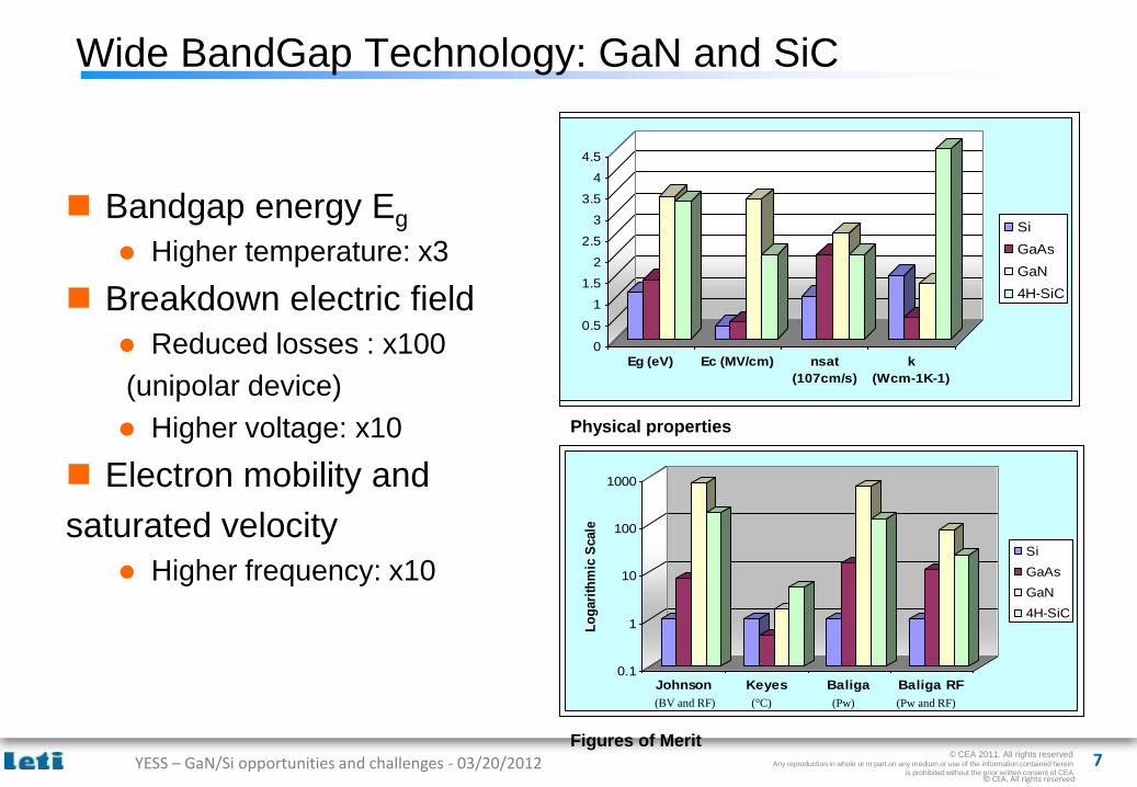
Wide BandGap Technology: GaN and SiC
0.1
1
10
100
1000
Lo
gari
thm
ic S
cale
Johnson Keyes Baliga Baliga RF
Si
GaAs
GaN
4H-SiC
Bandgap energy Eg
Higher temperature: x3
Breakdown electric field
Reduced losses : x100
(unipolar device)
Higher voltage: x10
Electron mobility and
saturated velocity
Higher frequency: x10
Figures of Merit
Physical properties
0
0.5
1
1.5
2
2.5
3
3.5
4
4.5
Eg (eV) Ec (MV/cm) nsat
(107cm/s)
k
(Wcm-1K-1)
Si
GaAs
GaN
4H-SiC
(BV and RF) (°C) (Pw) (Pw and RF)

© CEA 2011. All rights reserved Any reproduction in whole or in part on any medium or use of the information contained herein
is prohibited without the prior written consent of CEA © CEA. All rights reserved
YESS – GaN/Si opportunities and challenges - 03/20/2012 8
Positioning of GaN vs SiC & Si
Characteristics & Maturity of widebandgab materials
Limits of SiC / Si SiC Schottky Diodes commercial availability
Cost is the main issue
Substrate size
Opportunities for GaN Possibilities for substrates > 6 inches
Technology takes advantage of growth
in lighting and RF applications
Process with relaxed Temperature budget

© CEA 2011. All rights reserved Any reproduction in whole or in part on any medium or use of the information contained herein
is prohibited without the prior written consent of CEA © CEA. All rights reserved
YESS – GaN/Si opportunities and challenges - 03/20/2012 9
Positioning of GaN vs SiC & Si
GaN on Si
© CEA 2011. All rights reserved Any reproduction in whole or in part on any medium or use of the information contained herein
is prohibited without the prior written consent of CEA © CEA. All rights reserved
YESS – GaN/Si opportunities and challenges - 03/20/2012 10
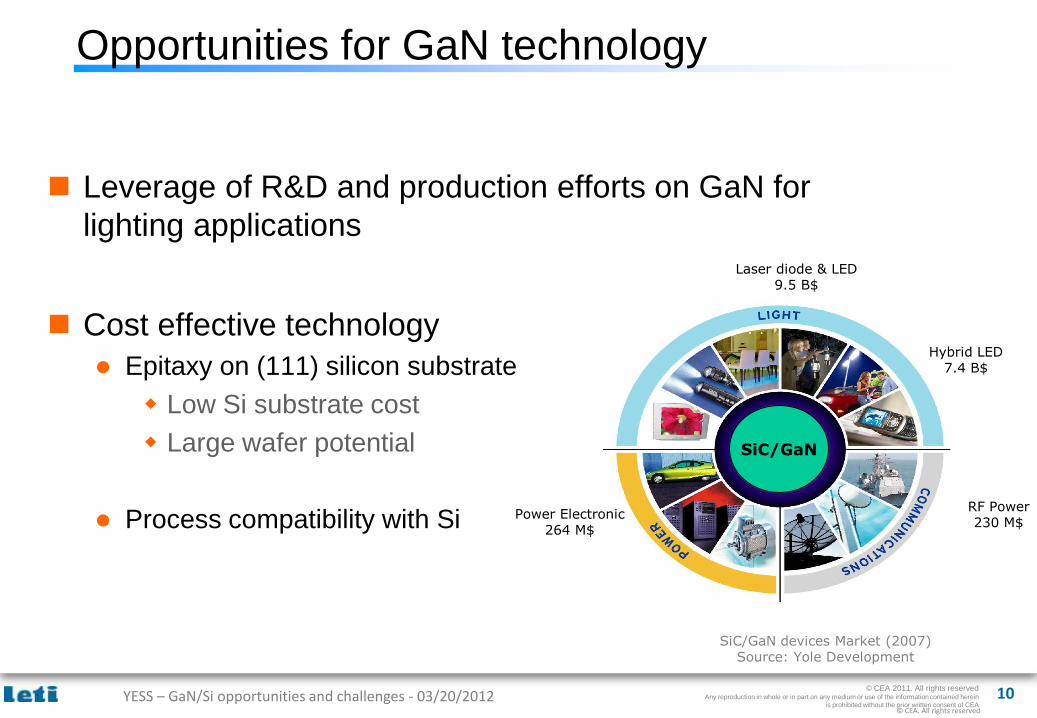
Opportunities for GaN technology
SiC/GaN
Hybrid LED 7.4 B$
Laser diode & LED 9.5 B$
Power Electronic 264 M$
RF Power 230 M$
SiC/GaN devices Market (2007) Source: Yole Development
Leverage of R&D and production efforts on GaN for
lighting applications
Cost effective technology
Epitaxy on (111) silicon substrate
Low Si substrate cost
Large wafer potential
Process compatibility with Si

© CEA 2011. All rights reserved Any reproduction in whole or in part on any medium or use of the information contained herein
is prohibited without the prior written consent of CEA © CEA. All rights reserved
YESS – GaN/Si opportunities and challenges - 03/20/2012 11
100W
1KW
10 KW
100 KW
2010 2012 2014 2016
Applications Roadmap for GaN power devices
Electric
Drive 600V, 10-20A
PV
Converters
Automotive
Hybrid/EV
600V , 30/50A
600V , 200 A
1200V, 100A Si IGBT SiC
Si MOSFET
Si IGBT
Si MOSFET Computing
Network
Com°
15V, 20-30A Servers &
Storage

© CEA 2011. All rights reserved Any reproduction in whole or in part on any medium or use of the information contained herein
is prohibited without the prior written consent of CEA © CEA. All rights reserved
YESS – GaN/Si opportunities and challenges - 03/20/2012 12
Value of GaN in various applications
DC/DC Convertors
Source : IR
Source : IR
Electric Drive
PV Panel Control
(Robustness,
Security)
© CEA 2011. All rights reserved Any reproduction in whole or in part on any medium or use of the information contained herein
is prohibited without the prior written consent of CEA © CEA. All rights reserved
YESS – GaN/Si opportunities and challenges - 03/20/2012 13
Outline
Context
Sustainability Policy and Power electronics
Power Electronics Requirements
Wide BandGap Technologies
GaN and SiC vs Silicon
GaN technology: a real opportunity?
GaN range of application
Challenges to be addressed

© CEA 2011. All rights reserved Any reproduction in whole or in part on any medium or use of the information contained herein
is prohibited without the prior written consent of CEA © CEA. All rights reserved
YESS – GaN/Si opportunities and challenges - 03/20/2012 14
State of the art in GaN transistor is based on RF HEMT
GaN on semi-insulating SiC
Key requirements need to be fulfill « low cost » and « high
voltage - high power - high frequency »
Low cost (silicon substrates) and ...
High breakdown voltage
Low Ron & high current operation
Vertical operation
Thick and high quality GaN epilayers on Silicon
High quality passivation and edge termination
MIS gate
Low Ron heterojunction, optimized bottom contact
Normally-off operation
Specific epilayers to control the conduction
High T° operation – thermal management
Devices transfer on metal (Copper)
Key requirements for GaN power transistors
Substrat résistif
GaN
GaN-AlGaN SiN, SiO2, …
Source Grille Drain
GaN-AlGaN Si3N4, SiO2, …
Source Grille Source
Drain

© CEA 2011. All rights reserved Any reproduction in whole or in part on any medium or use of the information contained herein
is prohibited without the prior written consent of CEA © CEA. All rights reserved
YESS – GaN/Si opportunities and challenges - 03/20/2012 15
Epitaxial layers : GaN on <111> Si substrates
SIMS analysis
Angular XPS in AlGaN
AFM surface analysis
EDX TEM Al in AlGaN
III-V Lab TEM structure
► Advanced characterization (TEM, TEM-EDX, AFM, SIMS, DRX, XPS,...)
• µ = 1650 cm2/V/s - R□ = 350 - 400 W
Plane view TEM
ToPoGaN1

© CEA 2011. All rights reserved Any reproduction in whole or in part on any medium or use of the information contained herein
is prohibited without the prior written consent of CEA © CEA. All rights reserved
YESS – GaN/Si opportunities and challenges - 03/20/2012 16
► Dielectric for passivation and MIS gate
MIS and passivation layers
2nm
2nm
2nm
2nm
2nm
2nm
2nm
2nm
2nm
2nm
AlGaN
Al2O3
HfO2
Al2O3
HfO2
Al2O3
HfO2
Al2O3
HfO2
Al2O3
HfO2
Grille
GaN
30nm
Si substrate
GaN active layer
Source Drain
Gate
AlN/GaN buffer
ToPoGaN1
1,0E-09
1,0E-08
1,0E-07
1,0E-06
1,0E-05
1,0E-04
1,0E-03
1,0E-02
1,0E-01
1,0E+00
-12 -10 -8 -6 -4 -2 0 2 4
ID (A
/mm
)
VG (V)
Schottky (Ni/Pt/Ti)
High-K MIS • Strong know-how in sub 32nm HighK
metal gate, reused for GaN devices
• ALD HfO2/Al2O3 multi-stack dielectric
• Mixed with SiN passivation
n xHfO2/Al2O3
© CEA 2011. All rights reserved Any reproduction in whole or in part on any medium or use of the information contained herein
is prohibited without the prior written consent of CEA © CEA. All rights reserved
YESS – GaN/Si opportunities and challenges - 03/20/2012 17
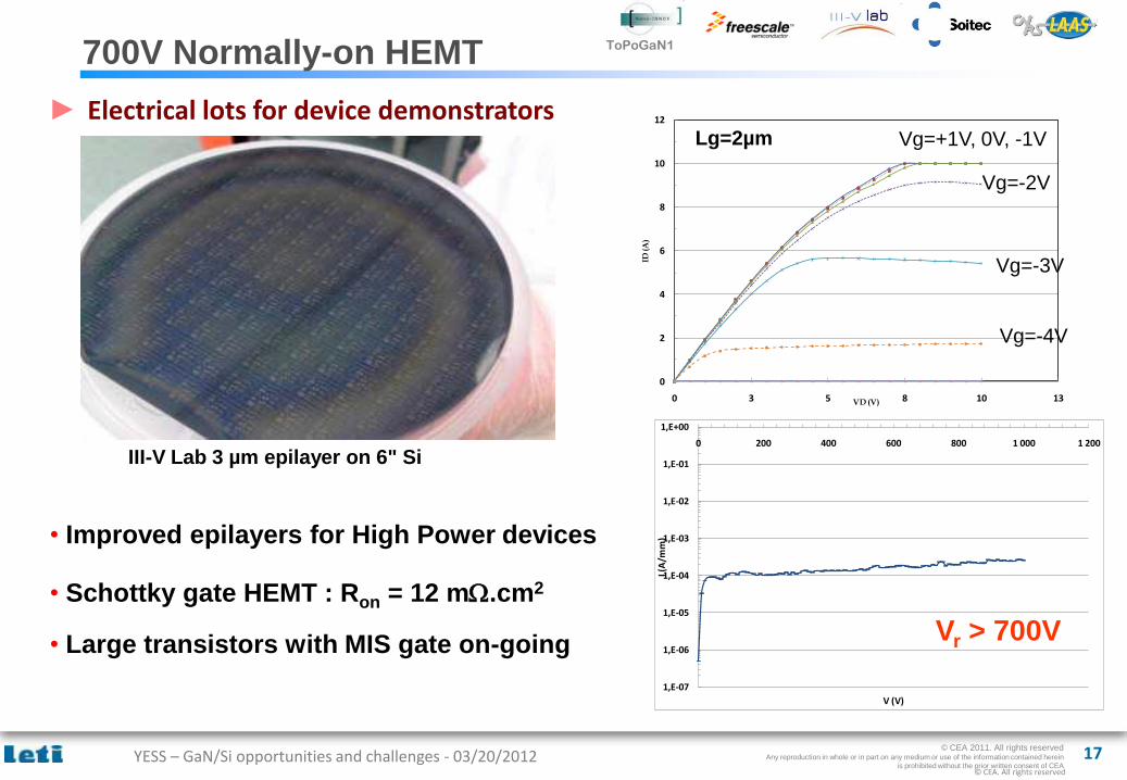
• Improved epilayers for High Power devices
• Schottky gate HEMT : Ron = 12 mW.cm2
• Large transistors with MIS gate on-going
700V Normally-on HEMT
1,E-07
1,E-06
1,E-05
1,E-04
1,E-03
1,E-02
1,E-01
1,E+00
0 200 400 600 800 1 000 1 200
I (A
/mm
)
V (V)
Vr > 700V
III-V Lab 3 µm epilayer on 6" Si
0
2
4
6
8
10
12
0 3 5 8 10 13
ID (A
)
VD (V)
Vg=+1V, 0V, -1V
Vg=-2V
Vg=-3V
Vg=-4V
Lg=2µm
► Electrical lots for device demonstrators
ToPoGaN1

© CEA 2011. All rights reserved Any reproduction in whole or in part on any medium or use of the information contained herein
is prohibited without the prior written consent of CEA © CEA. All rights reserved
YESS – GaN/Si opportunities and challenges - 03/20/2012 18
Packaging
► Packaging technology for High Temperature operating conditions
Qualification of low T sinterable Ag
High T polymer (LCP) and Metal Matrix Composites
From DBC to moulded multi-layer substrate using Powder Injection Moulding (PIM)
Chip on metal by direct bonding, for improved Rth
3D package Metal direct bonding

© CEA 2011. All rights reserved Any reproduction in whole or in part on any medium or use of the information contained herein
is prohibited without the prior written consent of CEA © CEA. All rights reserved
YESS – GaN/Si opportunities and challenges - 03/20/2012 19
Conclusions
GaN on Silicon Devices offers a wide range of
opportunities for new research topics
Engineering at the nanoscale is of the
essence
Many opportunities for cooperation between
French and US engineers and scientists

© CEA 2011. All rights reserved Any reproduction in whole or in part on any medium or use of the information contained herein
is prohibited without the prior written consent of CEA © CEA. All rights reserved
YESS – GaN/Si opportunities and challenges - 03/20/2012 20
Thanks for your attention