Embed Size (px)
Citation preview
GA - 5486AL
USER'S MANUAL
1. Please enable " EDO, 60ns DRAM or 40MHz CLK " in chipsetfeature setup, if EDO DRAM or 60ns FP DRAM or DX2-80 orDX4-120 is installed for the best performance.
2. To get top performance,you may set" DRAM Read Timing " to Fastest¡ B
" DRAM Write Timing " to Fastest¡ B
" SRAM Read Timing " to 2-1-1-1¡ Aif your CPU is DX4-100 or AMD5x86-P75 133MHz or Cx5x86-100/133 and your DRAM speed is 60ns.
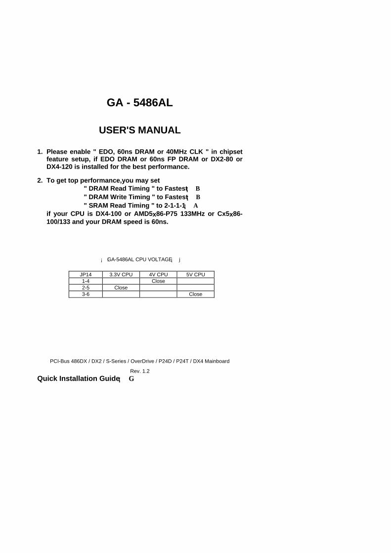
¡ iGA-5486AL CPU VOLTAGE¡ j
JP14 3.3V CPU 4V CPU 5V CPU1-4 Close2-5 Close3-6 Close
PCI-Bus 486DX / DX2 / S-Series / OverDrive / P24D / P24T / DX4 Mainboard
Rev. 1.2
Quick Installation Guide¡ G
GA-5486AL
2
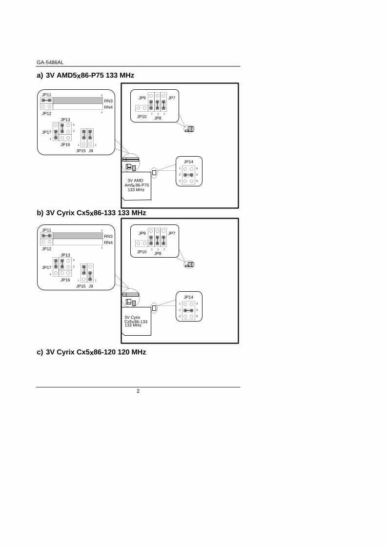
a) 3V AMD5x86-P75 133 MHz
JP11
JP12
RN3
RN4
JP16
JP14
JP13
J9JP15
JP17
1
2
3
4
5
6
1
3
4
1
1
1 1
111
JP8
JP7JP9
JP10
3V AMDAm5x 86-P75
133 MHz
b) 3V Cyrix Cx5x86-133 133 MHz
JP11
JP12
RN3
RN4
JP16
JP14
JP13
J9JP15
JP17
1
2
3
4
5
6
1
3
4
1
1
1 1
111
JP8
JP7JP9
JP10
3V CyrixCx5x86-133133 MHz
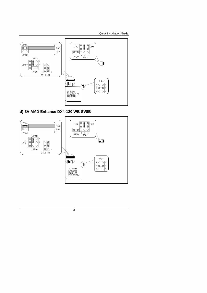
c) 3V Cyrix Cx5x86-120 120 MHz
Quick Installation Guide
3
JP11
JP12
RN3
RN4
JP16
JP14
JP13
J9JP15
JP17
1
2
3
4
5
6
1
3
4
1
1
1 1
111
JP8
JP7JP9
JP10
3V CyrixCx5x86-120120 MHz
d) 3V AMD Enhance DX4-120 WB SV8B
JP11
JP12
RN3
RN4
JP16
JP14
JP13
J9JP15
JP17
1
2
3
4
5
6
1
3
4
1
1
1 1
111
JP8
JP7JP9
JP10
3V AMDEnhanceDX4-120WB SV8B
GA-5486AL
4
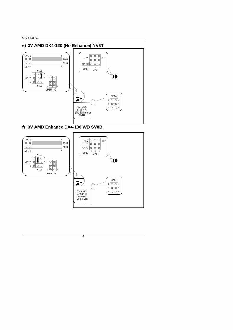
e) 3V AMD DX4-120 (No Enhance) NV8T
JP11
JP12
RN3
RN4
JP16
JP14
JP13
J9JP15
JP17
1
2
3
4
5
6
1
3
4
1
1
1 1
111
JP8
JP7JP9
JP10
3V AMD DX4-120(No Enhance) NV8T
f) 3V AMD Enhance DX4-100 WB SV8B
JP11
JP12
RN3
RN4
JP16
JP14
JP13
J9JP15
JP17
1
2
3
4
5
6
1
3
4
1
1
1 1
111
JP8
JP7JP9
JP10
3V AMDEnhanceDX4-100WB SV8B
Quick Installation Guide
5
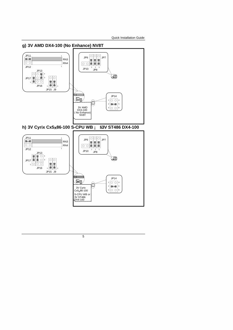
g) 3V AMD DX4-100 (No Enhance) NV8T
JP11
JP12
RN3
RN4
JP16
JP14
JP13
J9JP15
JP17
1
2
3
4
5
6
1
3
4
1
1
1 1
111
JP8
JP7JP9
JP10
3V AMD DX4-100( No Enhance) NV8T
h) 3V Cyrix Cx5x86-100 S-CPU WB ¡ ® 3V ST486 DX4-100
JP11
JP12
RN3
RN4
JP16
JP14
JP13
J9JP15
JP17
1
2
3
4
5
6
1
3
4
1
1
1 1
111
JP8
JP7JP9
JP10
3V Cyrixx
S-CPU WB or3V ST486 DX4-100
Cx5 86-100
GA-5486AL
6
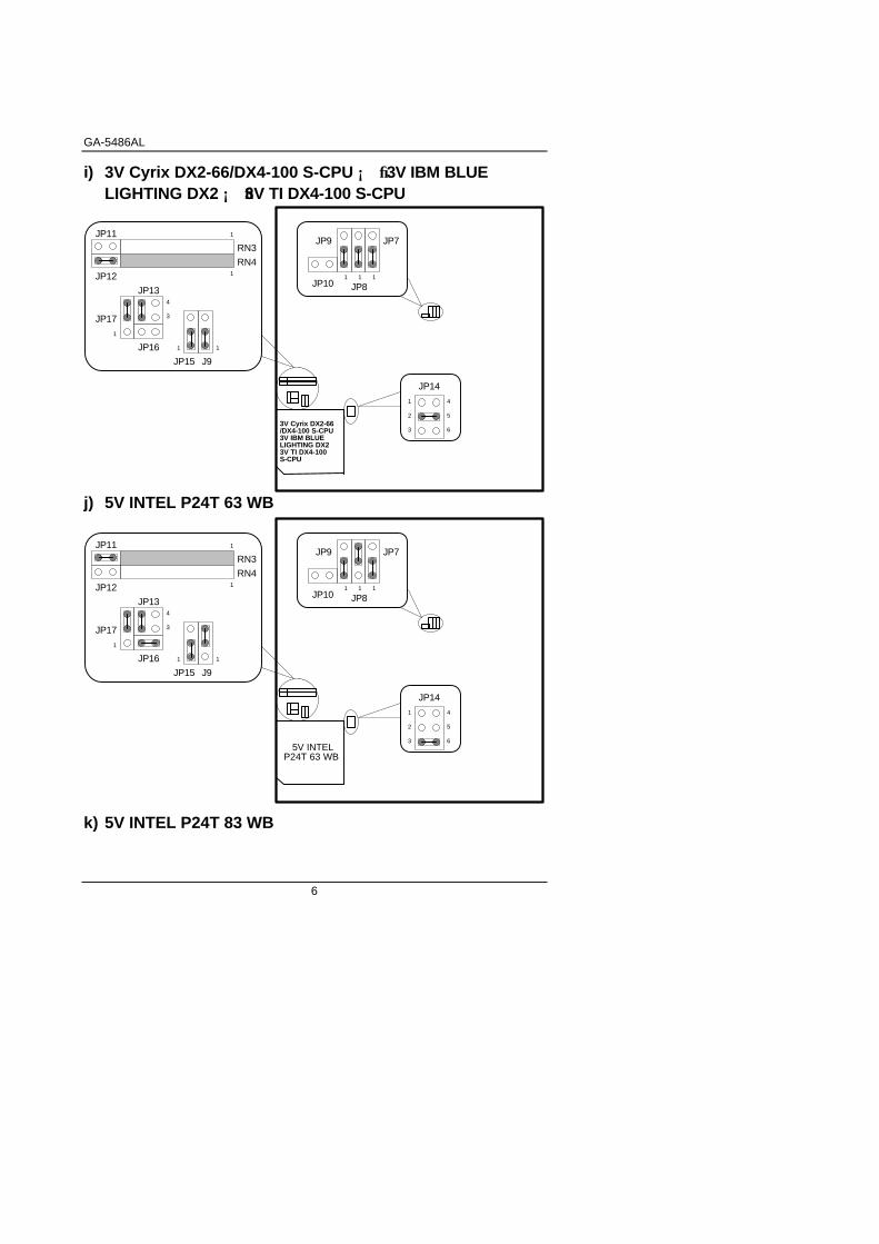
i) 3V Cyrix DX2-66/DX4-100 S-CPU ¡ ® 3V IBM BLUELIGHTING DX2 ¡ ®3V TI DX4-100 S-CPU
JP11
JP12
RN3
RN4
JP16
JP14
JP13
J9JP15
JP17
1
2
3
4
5
6
1
3
4
1
1
1 1
111
JP8
JP7JP9
JP10
3V Cyrix DX2-66 /DX4-100 S-CPU3V IBM BLUE LIGHTING DX23V TI DX4-100S-CPU
j) 5V INTEL P24T 63 WB
JP11
JP12
RN3
RN4
JP16
JP14
JP13
J9JP15
JP17
1
2
3
4
5
6
1
3
4
1
1
1 1
111
JP8
JP7JP9
JP10
5V INTELP24T 63 WB
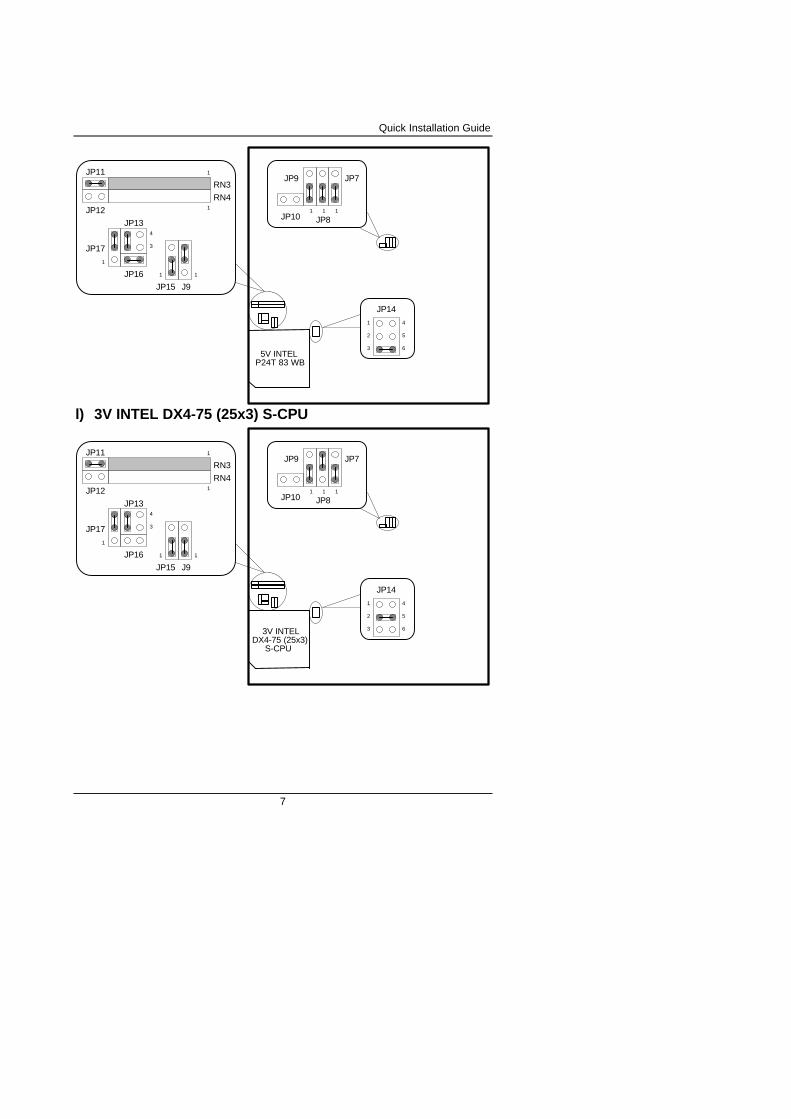
k) 5V INTEL P24T 83 WB
Quick Installation Guide
7
JP11
JP12
RN3
RN4
JP16
JP14
JP13
J9JP15
JP17
1
2
3
4
5
6
1
3
4
1
1
1 1
111
JP8
JP7JP9
JP10
5V INTELP24T 83 WB
l) 3V INTEL DX4-75 (25x3) S-CPU
JP11
JP12
RN3
RN4
JP16
JP14
JP13
J9JP15
JP17
1
2
3
4
5
6
1
3
4
1
1
1 1
111
JP8
JP7JP9
JP10
3V INTELDX4-75 (25x3) S-CPU
GA-5486AL
8
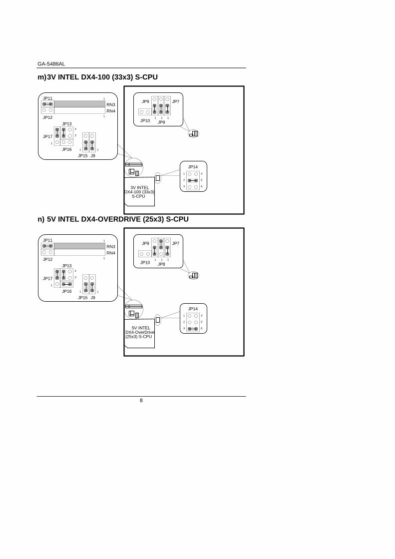
m)3V INTEL DX4-100 (33x3) S-CPU
JP11
JP12
RN3
RN4
JP16
JP14
JP13
J9JP15
JP17
1
2
3
4
5
6
1
3
4
1
1
1 1
111
JP8
JP7JP9
JP10
3V INTELDX4-100 (33x3) S-CPU
n) 5V INTEL DX4-OVERDRIVE (25x3) S-CPU
JP11
JP12
RN3
RN4
JP16
JP14
JP13
J9JP15
JP17
1
2
3
4
5
6
1
3
4
1
1
1 1
111
JP8
JP7JP9
JP10
5V INTEL DX4-OverDrive (25x3) S-CPU
Quick Installation Guide
9
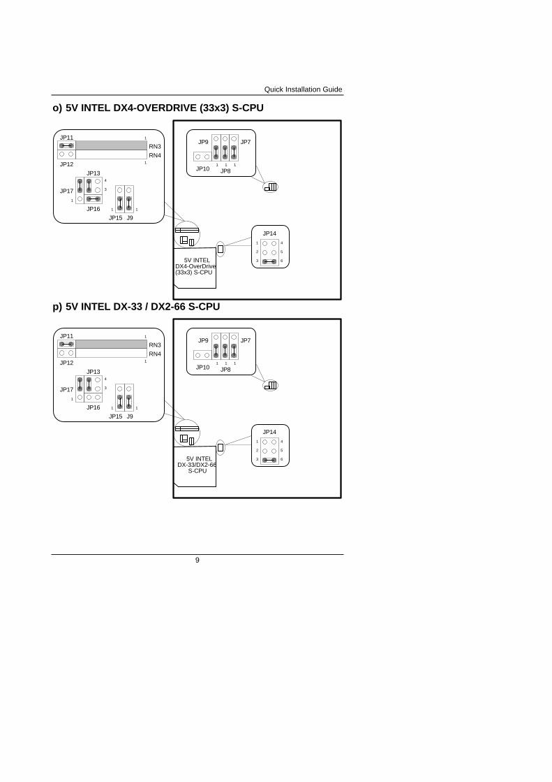
o) 5V INTEL DX4-OVERDRIVE (33x3) S-CPU
JP11
JP12
RN3
RN4
JP16
JP14
JP13
J9JP15
JP17
1
2
3
4
5
6
1
3
4
1
1
1 1
111
JP8
JP7JP9
JP10
5V INTEL DX4-OverDrive (33x3) S-CPU
p) 5V INTEL DX-33 / DX2-66 S-CPU
JP11
JP12
RN3
RN4
JP16
JP14
JP13
J9JP15
JP17
1
2
3
4
5
6
1
3
4
1
1
1 1
111
JP8
JP7JP9
JP10
5V INTEL DX-33/DX2-66 S-CPU
GA-5486AL
10
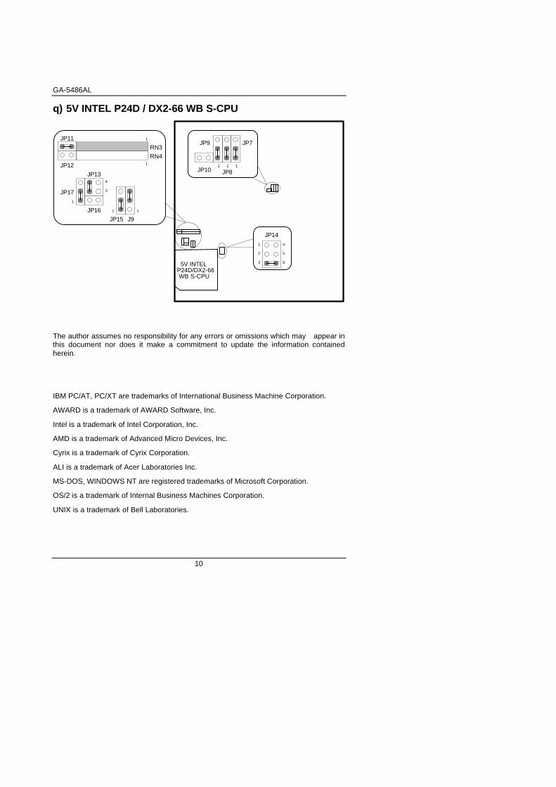
q) 5V INTEL P24D / DX2-66 WB S-CPU
JP11
JP12
RN3
RN4
JP16
JP14
JP13
J9JP15
JP17
1
2
3
4
5
6
1
3
4
1
1
1 1
111
JP8
JP7JP9
JP10
5V INTELP24D/DX2-66 WB S-CPU
The author assumes no responsibility for any errors or omissions which may appear inthis document nor does it make a commitment to update the information containedherein.
IBM PC/AT, PC/XT are trademarks of International Business Machine Corporation.
AWARD is a trademark of AWARD Software, Inc.
Intel is a trademark of Intel Corporation, Inc.
AMD is a trademark of Advanced Micro Devices, Inc.
Cyrix is a trademark of Cyrix Corporation.
ALI is a trademark of Acer Laboratories Inc.
MS-DOS, WINDOWS NT are registered trademarks of Microsoft Corporation.
OS/2 is a trademark of Internal Business Machines Corporation.
UNIX is a trademark of Bell Laboratories.
Table of Contents
1
Table of Contents
1.INTRODUCTION ......................................................................................................... 1-1
1.1.PREFACE ............................................................................................................. 1-1
1.2.KEY FEATURES................................................................................................... 1-1
1.3.PERFORMANCE LIST ......................................................................................... 1-2
1.4.BLOCK DIAGRAM................................................................................................ 1-3
1.5. INTRODUCE THE PCI-BUS ................................................................................ 1-4
2.SPECIFICATION......................................................................................................... 2-1
2.1.HARDWARE ......................................................................................................... 2-1
2.2.SOFTWARE.......................................................................................................... 2-2
2.3.ENVIRONMENT ................................................................................................... 2-2
3.HARDWARE INSTALLATION .................................................................................... 3-1
3.1.UNPACKING......................................................................................................... 3-1
3.2.MAINBOARD LAYOUT......................................................................................... 3-2
3.3.JUMPERS AND CONNECTORS SETTING........................................................ 3-2
3.4.SRAM INSTALLATION AND JUMPERS SETUP................................................ 3-3
3.5.CPU INSTALLATION AND JUMPERS SETUP................................................... 3-4
3.6.DRAM INSTALLATION......................................................................................... 3-6
3.7.SPEAKER CONNECTOR INSTALLATION ......................................................... 3-6
3.8.POWER LED & KEY LOCK CONNECTOR INSTALLATION ............................. 3-6
3.9.TURBO SWITCH CONNECTOR INSTALLATION.............................................. 3-7
3.10.TURBO LED FLASH GREEN LED CONNECTOR INSTALLATION ................ 3-7
3.11.HARDWARE RESET SWITCH CONNECTOR INSTALLATION ...................... 3-7
3.12.GREEN FUNCTION INSTALLATION ................................................................ 3-8
3.13.PERIPHERAL DEVICE INSTALLATION............................................................ 3-8
4.BIOS CONFIGURATION ............................................................................................ 4-1
4.1.ENTERING SETUP .............................................................................................. 4-1
4.2.CONTROL KEYS.................................................................................................. 4-1
4.3.GETTING HELP.................................................................................................... 4-2
4.3.1.Main Menu ................................................................................................... 4-2
4.3.2.Status Page Setup Menu / Option Page Setup Menu................................ 4-2
GA-5486AL
2
4.4.THE MAIN MENU ................................................................................................. 4-2
4.5.STANDARD CMOS SETUP MENU ..................................................................... 4-4
4.6.BIOS FEATURES SETUP.................................................................................... 4-7
4.7.CHIPSET FEATURES SETUP............................................................................. 4-9
4.8.POWER MANAGEMENT SETUP........................................................................ 4-12
4.9.PCI CONFIGURATION SETUP ........................................................................... 4-14
4.10.LOAD BIOS DEFAULTS..................................................................................... 4-16
4.11.LOAD SETUP DEFAULTS ................................................................................. 4-17
4.12.SUPERVISOR PASSWORD .............................................................................. 4-18
4.13.USER PASSWORD ............................................................................................ 4-19
4.14.IDE HDD AUTO DETECTION ............................................................................ 4-20
4.15.HDD LOW LEVEL FORMAT .............................................................................. 4-20
4.16.SAVE & EXIT SETUP ......................................................................................... 4-21
4.17.EXIT WITHOUT SAVING.................................................................................... 4-22
4.18.KEYBOARD SETTING FUNCTION ................................................................... 4-22
5.AT TECHNICAL INFORMATION................................................................................ 5-1
5.1.BUS CONNECTOR PIN OUT .............................................................................. 5-1
5.1.1.ISA BUS SLOT PIN OUT ............................................................................ 5-1
5.1.2.PCI BUS SLOT PIN OUT............................................................................ 5-2
5.2. I/O & MEMORY MAP............................................................................................ 5-3
5.3.TIMER & DMA CHANNELS MAP ........................................................................ 5-3
5.4. INTERRUPT MAP................................................................................................. 5-4
5.5.RTC & CMOS RAM MAP ..................................................................................... 5-4
APPENDIX A: POST MESSAGE ................................................................................... A-1
APPENDIX B: POST CODES ........................................................................................ B-1
APPENDIX C: BIOS DEFAULT DRIVE TABLE ............................................................ C-1
APPENDIX D: PROBLEM SHEET................................................................................. D-1
Introduction
1-1
1INTRODUCTION
1.1 PREFACE
Welcome to use the GA-5486AL motherboard. The motherboard is a 128 KB - 512 KBCACHE 5x86 & 486DX series PC/AT compatible system with ISA bus, PCI (PeripheralComponent Interconnect) bus and has been designed to be the fastest 5x86 & 486PC/AT system and the GREEN FUNCTION (Power-Down Mode) had been added.There are some new features allowing you to operate the system with just theperformance you want.
This manual also explains how to install the motherboard for operation, and how to setup your CMOS CONFIGURATION with BIOS SETUP program.
1.2 KEY FEATURES
• 5x86 & 80486 based PC/AT compatible mainboard with ISA and PCI Bus.
• Supports 3 Master PCI bus slots .
• Supports AMD5x86 / Cx5x86 / 486DX / DX2 / S-Series / OverDrive / P24D / P24T /DX4 running at 25 - 133 MHz.
• Supports True Green Function.
• Supports Intel, AMD, Cyrix, TI, IBM CPU.
• Supports 237 pin (Socket 3) ZIF White socket / LIF socket on board.
• Supports 128 / 256 / 512 KB 2nd cache memory operated in BURST mode.
• Write-Back cache operation.
• Supports 2 - 128 MB DRAM memory on board.
• Supports 2 channels Enhance PCI IDE ports for 4 IDE Devices.
• Supports 2xCOM (16550) ports, 1xLPT (EPP / ECP) port, 1 Floppy port.
• Supports shadow RAM for BIOS & VIDEO BIOS.
• Supports shadow RAM cacheable function to improve performance.
• Supports Hardware & Software speed change function.
• Licensed AWARD BIOS.
• 2/3 Baby AT size (22 cm x 21 cm) with 4 AT slots and 3 PCI slots .
1.3 PERFORMANCE LIST
GA-5486AL
1-2
The following performance data list is the testing results with some popular benchmarktesting programs. These data are just reference for users and there is no responsibilityfor different testing data values gotten by users.( The different H/W & S/W configurationwill result in different benchmark testing results.)
System Benchmarks At DOS Environment with IDE Controller
• CPU : AMD5x86-133/ Cx5x86-100/ DX4-100 OVER/ Cx5x86-133/ AMD DX4-100 WB/ Cyrix DX4-100/ P24T-63
• DRAM : 8 MB / 60ns 2pcs. Total memory 16MB
• CACHE : 256KB
• VGA : ATi mach 64V
• H.D. : Quantum ( 1GB )
• O.S. : MS DOS V6.22
• Autoexec.bat: • Config.sys:
C:\DOS\SMARTDRV.EXE/X
device = c:\alihdd\alihdd.sys /t /s33 /bios:yyyy /drive:hnnn /PIO:aaaa /bkm:yyyy /
@ECHO OFF DEVICE = C:\DOS\SETVER.EXE
PROMPT $p$g DEVICE = \WINDOWS\HIMEM.SYS
PATH C:\;C:\DOS DOS = HIGH
SET TEMP = C:\DOS FILES = 30
DEVICE = C:\WINDOWS\IFSHLP.SYS
STACK = 9,256
×256KØ
Software Item Unit Cx5x86-133 AMD5x86-133 Cx5x86-100 DX4-100 OVER
LandMark Speed CPU MHz 565.13 447.09 423.85 364.11V2.0 FPU MHz 1415.36 1092.82 1061.50 820.42Norton SI V8.0 CPU index 352.7 288.7 264.5 198.5Power Meter V1.81 MIPS Mips 65.0 57.3 48.7 40.6PC Bench mark DOS Mark index 761.97 701.37 678.32 632.94V9.0 CPU mark 16 index 150.09 129.85 126.30 119.19Winstone 95 640 X 480 X 256 155.2 145.5 136.7 129
Software Item Unit P24T-63 AMD DX4-100 WB Cyrix DX4-100
LandMark Speed CPU MHz 361.42 335.30 330.63V2.0 FPU MHz 1040.46 819.60 868.54Norton SI V8.0 CPU index 198.5 216.5 170.1Power Meter V1.81 MIPS Mips 39.8 43.8 39.4PC Bench mark DOS Mark index 586.49 582.47 574.98V9.0 CPU mark 16 index 116.37 105.01 103.25Winstone 95 640 X 480 X 256 122.3 118.6 111.4
Introduction
1-3
×EDO RAM NON-CACHEØ
Software Item Unit Cx5x86-133 AMD5x86-133 Cx5x86-100 DX4-100 OVER
LandMark Speed CPU MHz 565.16 447.11 423.86 363.92V2.0 FPU MHz 1415.48 1092.90 1061.85 818.52Norton SI V8.0 CPU index 352.7 288.7 264.6 198.5Power Meter V1.81 MIPS Mips 65.0 58.2 48.7 34.5PC Bench mark DOS Mark index 726.90 677.56 645.49 553.44V9.0 CPU mark 16 index 129.17 118.86 111.41 90.83Winstone 95 640 X 480 X 256 149.3 141.9 132.8 116.4
Software Item Unit P24T-63 AMD DX4-100 WB Cyrix DX4-100
LandMark Speed CPU MHz 361.48 335.32 330.63V2.0 FPU MHz 1040.64 819.64 868.58Norton SI V8.0 CPU index 198.5 216.5 170.1Power Meter V1.81 MIPS Mips 41.0 44.3 39.4PC Bench mark DOS Mark index 603.5 554.12 548.18V9.0 CPU mark 16 index 116.01 97.21 93.32Winstone 95 640 X 480 X 256 122.1 111.9 105.1
1.4 BLOCK DIAGRAM
SRAMX4
ROM
RTC
KBC
optional
optional
IDE
TAGSRAM
TAG
DRAM4
BANK
CPU
GA[26:2]
GA31
CMP
M1489
LINK_BUS
PCI
IBCM1487
ISASD SA
XDGA[9:2]
GA[17:2]
GD GAHOST
×Figure 1.1Ø
GA-5486AL
1-4
1.5 INTRODUCE THE PCI-BUS
Connecting devices to a local bus of CPU can dramatically increase the speed of I/O-bound peripherals with only a slight increase in cost over traditional systems. Thisprice/performance point has created a vast market potential for local bus products. Themain barrier to this market has been the lack of an accepted standard for local busperipherals.
The PCI-bus standard, under development since Jun. 1992, which is designed to bringworkstation-level performance to standard PC platform. The PCI-bus removes many ofthe bottlenecks that have hampered PC for several years. On the PCI-bus, peripheralsoperate at the native speed of the computer system, thus enabling data transferbetween peripherals and the system at maximum speed. This performance is critical forbandwidth-constrained devices such as video, multimedia, mass storage andnetworking adapters.
PCI-bus standard provide end-users with a low-cost, extendible and portable local busdesign, which will allow systems and peripherals from different manufacturers to worktogether.
Specification
2-1
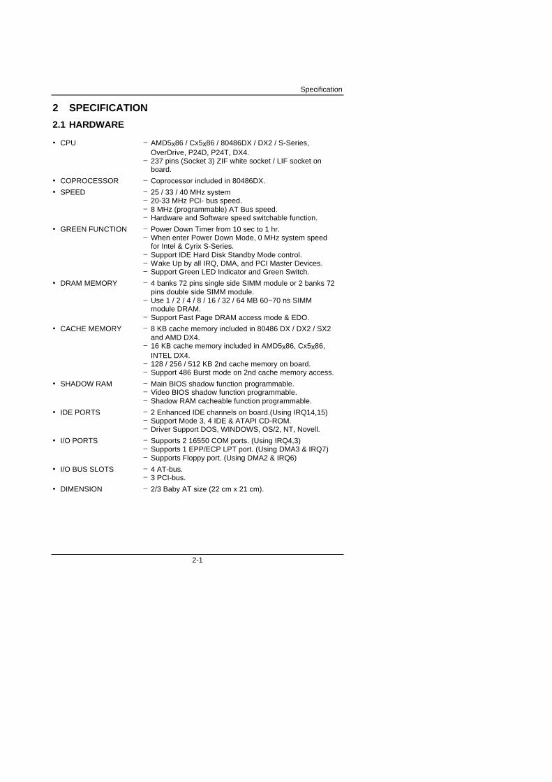
2 SPECIFICATION
2.1 HARDWARE
• CPU − AMD5x86 / Cx5x86 / 80486DX / DX2 / S-Series,OverDrive, P24D, P24T, DX4.
− 237 pins (Socket 3) ZIF white socket / LIF socket onboard.
• COPROCESSOR − Coprocessor included in 80486DX.
• SPEED − 25 / 33 / 40 MHz system− 20-33 MHz PCI- bus speed.− 8 MHz (programmable) AT Bus speed.− Hardware and Software speed switchable function.
• GREEN FUNCTION − Power Down Timer from 10 sec to 1 hr.− When enter Power Down Mode, 0 MHz system speed
for Intel & Cyrix S-Series.− Support IDE Hard Disk Standby Mode control.− Wake Up by all IRQ, DMA, and PCI Master Devices.− Support Green LED Indicator and Green Switch.
• DRAM MEMORY − 4 banks 72 pins single side SIMM module or 2 banks 72pins double side SIMM module.
− Use 1 / 2 / 4 / 8 / 16 / 32 / 64 MB 60~70 ns SIMMmodule DRAM.
− Support Fast Page DRAM access mode & EDO.
• CACHE MEMORY − 8 KB cache memory included in 80486 DX / DX2 / SX2and AMD DX4.
− 16 KB cache memory included in AMD5x86, Cx5x86,INTEL DX4.
− 128 / 256 / 512 KB 2nd cache memory on board.− Support 486 Burst mode on 2nd cache memory access.
• SHADOW RAM − Main BIOS shadow function programmable.− Video BIOS shadow function programmable.− Shadow RAM cacheable function programmable.
• IDE PORTS − 2 Enhanced IDE channels on board.(Using IRQ14,15)− Support Mode 3, 4 IDE & ATAPI CD-ROM.− Driver Support DOS, WINDOWS, OS/2, NT, Novell.
• I/O PORTS − Supports 2 16550 COM ports. (Using IRQ4,3)− Supports 1 EPP/ECP LPT port. (Using DMA3 & IRQ7)− Supports Floppy port. (Using DMA2 & IRQ6)
• I/O BUS SLOTS − 4 AT-bus.− 3 PCI-bus.
• DIMENSION − 2/3 Baby AT size (22 cm x 21 cm).
GA-5486AL
2-2
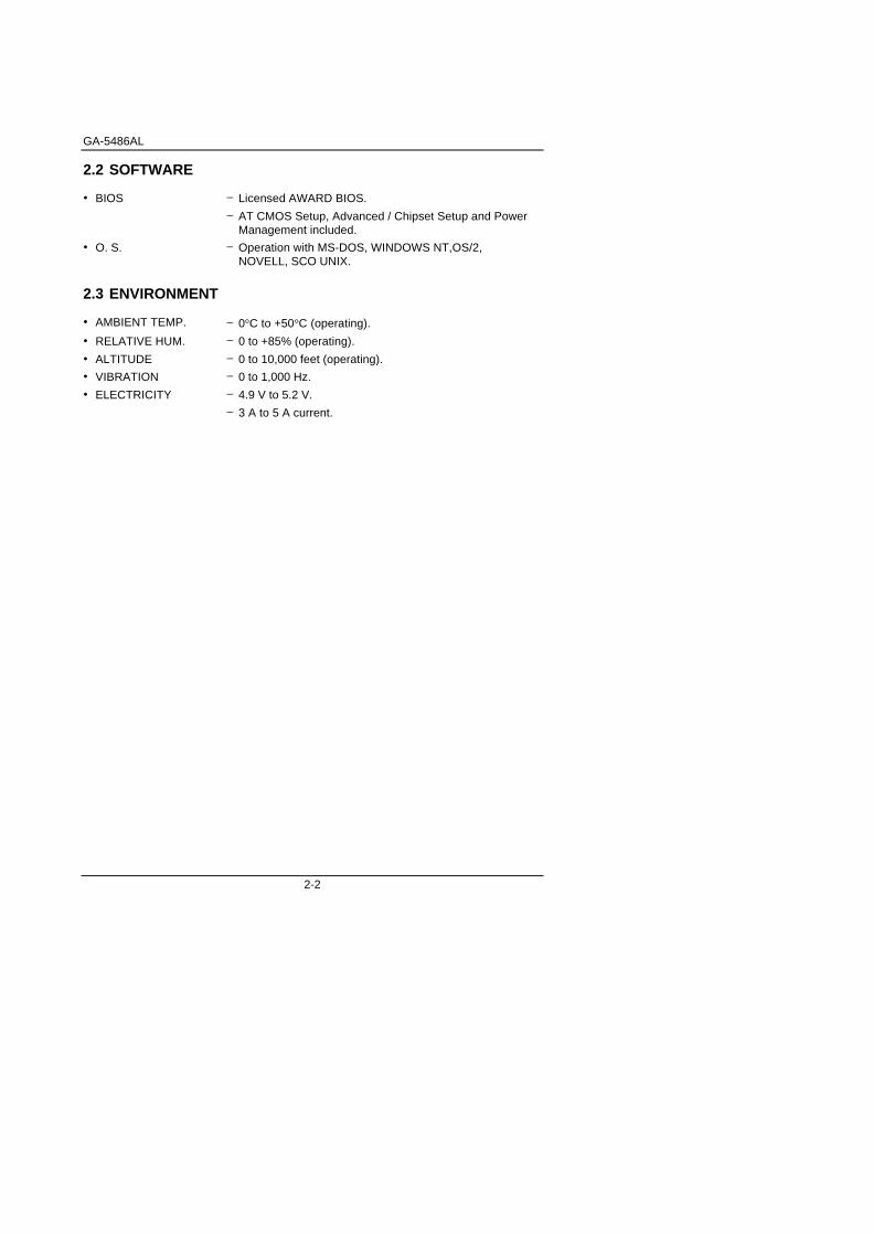
2.2 SOFTWARE
• BIOS − Licensed AWARD BIOS.
− AT CMOS Setup, Advanced / Chipset Setup and PowerManagement included.
• O. S. − Operation with MS-DOS, WINDOWS NT,OS/2,NOVELL, SCO UNIX.
2.3 ENVIRONMENT
• AMBIENT TEMP. − 0°C to +50°C (operating).
• RELATIVE HUM. − 0 to +85% (operating).
• ALTITUDE − 0 to 10,000 feet (operating).
• VIBRATION − 0 to 1,000 Hz.
• ELECTRICITY − 4.9 V to 5.2 V.
− 3 A to 5 A current.
Hardware Installation
3-1
3 HARDWARE INSTALLATION
3.1 UNPACKING
The ainboard ackage hould ontain he ollowing:
• The A-5486AL ainboard
• User's manual
• A Driver Diskette
The mainboard contains sensitive electric components which can be easily damaged bystatic electricity, so the mainboard should be left in its original packing until it is installed.
Unpacking and installation should be done on a grounded anti-static mat. The operatorshould be wearing an anti static wristband, grounded at the same point as the anti-staticmat.
Inspect the mainboard carton for obvious damage. Shipping and handling may causedamage to your board. Be sure there are no shipping and handling damages on theboard before proceeding.
After opening the mainboard carton, extract the system board and place it only on agrounded anti-static surface component side up. Again inspect the board for damage.Press down on all of the socket IC's to make sure that they are properly seated. Do thisonly on with the board placed on a firm flat surface.
M Do not apply power to the board if it has been damaged..
You are now ready to install your mainboard. The mounting hole pattern on themainboard matches the IBM-XT system board. It is assumed that the chassis isdesigned for a standard IBM XT/AT mainboard mounting.
Place the chassis on the anti-static mat and remove the cover. Take the plastic clips,Nylon stand-off and screws for mounting the system board, and keep them separate.
GA-5486AL
3-2
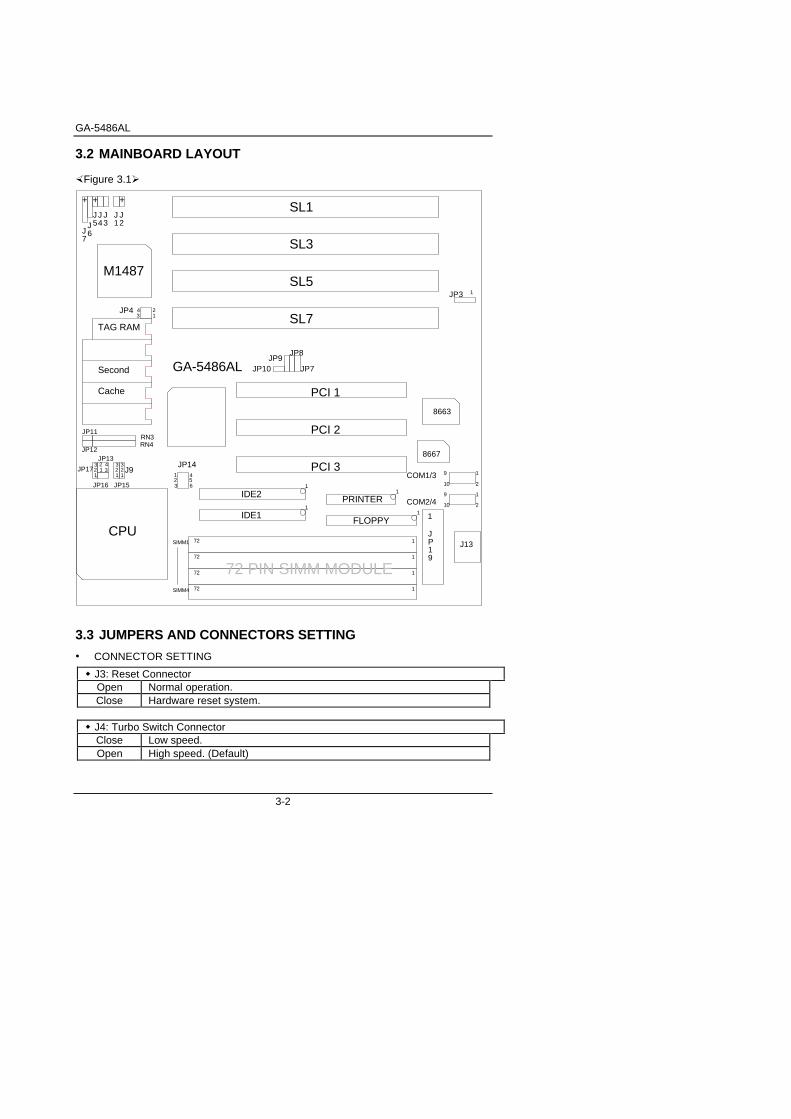
3.2 MAINBOARD LAYOUT
×Figure 3.1Ø
+ + +
J7
J6
J5
J4
J3
J2
J1
M1487
TAG RAM
Second
Cache
JP11
JP12
JP17
JP13
JP16
J9
CPU
SL1
SL7
SL5
SL3
JP10JP9
JP8
JP7
PCI 1
PCI 3
PCI 2
JP14
8663
8667
COM1/3
COM2/4
1
2
9
10
1
2
9
10
IDE2
IDE1
PRINTER
FLOPPYJP19
J13SIMM1
SIMM4
1JP3
GA-5486AL
12
34JP4
RN3RN4
123
12
34
123
123
JP15
123
456
1
1
1
1
1
72 PIN SIMM MODULE
72
72
72
72
1
1
1
1
3.3 JUMPERS AND CONNECTORS SETTING
• CONNECTOR SETTING
w J3: Reset ConnectorOpen Normal operation.Close Hardware reset system.
w J4: Turbo Switch ConnectorClose Low speed.Open High speed. (Default)
Hardware Installation
3-3
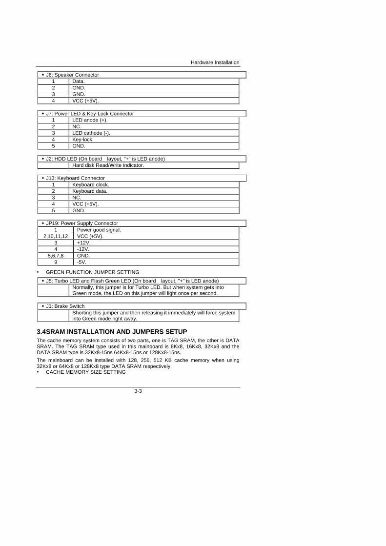
w J6: Speaker Connector1 Data.2 GND.3 GND.4 VCC (+5V).
w J7: Power LED & Key-Lock Connector1 LED anode (+).2 NC.3 LED cathode (-).4 Key-lock.5 GND.
w J2: HDD LED (On board layout, "+" is LED anode)Hard disk Read/Write indicator.
w J13: Keyboard Connector1 Keyboard clock.2 Keyboard data.3 NC.4 VCC (+5V).5 GND.
w JP19: Power Supply Connector1 Power good signal.
2,10,11,12 VCC (+5V).3 +12V.4 -12V.
5,6,7,8 GND.9 -5V.
• GREEN FUNCTION JUMPER SETTING
w J5: Turbo LED and Flash Green LED (On board layout, "+" is LED anode)Normally, this jumper is for Turbo LED. But when system gets intoGreen mode, the LED on this jumper will light once per second.
w J1: Brake SwitchShorting this jumper and then releasing it immediately will force systeminto Green mode right away.
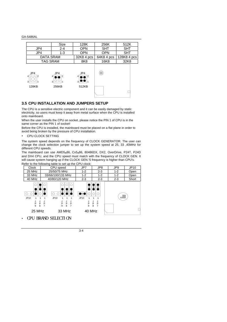
3.4SRAM INSTALLATION AND JUMPERS SETUPThe cache memory system consists of two parts, one is TAG SRAM, the other is DATASRAM. The TAG SRAM type used in this mainboard is 8Kx8, 16Kx8, 32Kx8 and theDATA SRAM type is 32Kx8-15ns 64Kx8-15ns or 128Kx8-15ns.
The mainboard can be installed with 128, 256, 512 KB cache memory when using32Kx8 or 64Kx8 or 128Kx8 type DATA SRAM respectively.• CACHE MEMORY SIZE SETTING
GA-5486AL
3-4
Size 128K 256K 512KJP4 2-4 OPN SHT SHTJP4 1-3 OPN OPN SHT
DATA SRAM 32K8 4 pcs 64K8 4 pcs 128K8 4 pcsTAG SRAM 8K8 16K8 32K8
JP4
1
2
3
4JP4
1
2
3
4JP4
1
2
3
4
128KB 512KB256KB
3.5 CPU INSTALLATION AND JUMPERS SETUPThe CPU is a sensitive electric component and it can be easily damaged by staticelectricity, so users must keep it away from metal surface when the CPU is installedonto mainboard.When the user installs the CPU on socket, please notice the PIN 1 of CPU is in thesame corner as the PIN 1 of socket!Before the CPU is installed, the mainboard must be placed on a flat plane in order toavoid being broken by the pressure of CPU installation.
• CPU CLOCK SETTING
The system speed depends on the frequency of CLOCK GENERATOR. The user canchange the clock selection jumper to set up the system speed at 25, 33 ,40MHz fordifferent CPU speeds.The mainboard can use AMD5x86, Cx5x86, 80486DX, DX2, OverDrive, P24T, P24Dand DX4 CPU, and the CPU speed must match with the frequency of CLOCK GEN. Itwill cause system hanging up if the CLOCK GEN.'S frequency is higher than CPU's.Refer to the following table to set up the CPU clock:
Clock CPU speed JP7 JP8 JP9 JP1025 MHz 25/50/75 MHz 1-2 2-3 1-2 Open33 MHz 33/66/100/133 MHz 1-2 1-2 1-2 Open40 MHz 40/80/120 MHz 2-3 2-3 2-3 Short
JP7
JP8
JP9
JP10
JP7
JP8
JP9
JP10
JP7
JP8
JP9
JP10
25 MHz 33 MHz 40 MHz
1 1 1 1 1 1 1 1 1
• CPU BRAND SELECTION
Hardware Installation
3-5
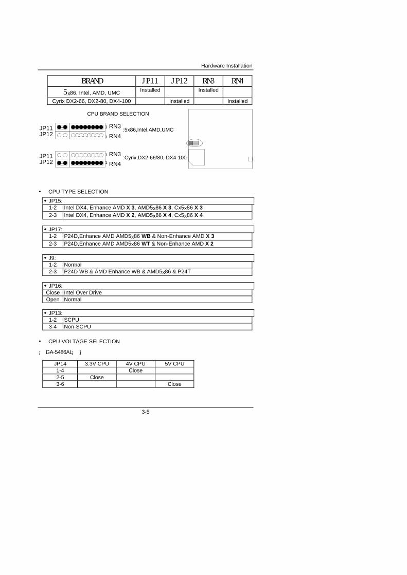
BRAND JP11 JP12 RN3 RN4
5x86, Intel, AMD, UMC Installed Installed
Cyrix DX2-66, DX2-80, DX4-100 Installed Installed
1
1
RN3
RN4
CPU BRAND SELECTION
:5x86,Intel,AMD,UMC
1
1
RN3
RN4
:Cyrix,DX2-66/80, DX4-100
JP11JP12
JP11JP12
• CPU TYPE SELECTION
w JP15:1-2 Intel DX4, Enhance AMD X 3, AMD5x86 X 3, Cx5x86 X 32-3 Intel DX4, Enhance AMD X 2, AMD5x86 X 4, Cx5x86 X 4
w JP17:1-2 P24D,Enhance AMD AMD5x86 WB & Non-Enhance AMD X 32-3 P24D,Enhance AMD AMD5x86 WT & Non-Enhance AMD X 2
w J9:1-2 Normal2-3 P24D WB & AMD Enhance WB & AMD5x86 & P24T
w JP16:Close Intel Over DriveOpen Normal
w JP13:1-2 SCPU3-4 Non-SCPU
• CPU VOLTAGE SELECTION
¡ iGA-5486AL¡ j
JP14 3.3V CPU 4V CPU 5V CPU1-4 Close2-5 Close3-6 Close
GA-5486AL
3-6
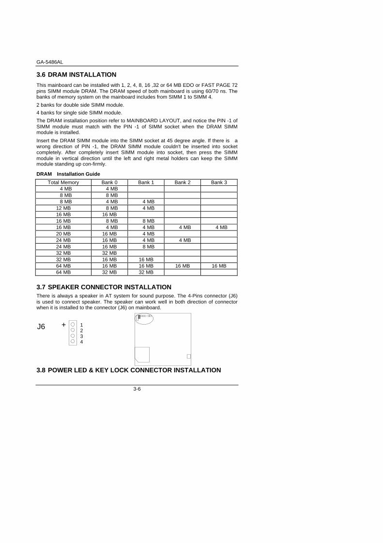
3.6 DRAM INSTALLATION
This mainboard can be installed with 1, 2, 4, 8, 16 ,32 or 64 MB EDO or FAST PAGE 72pins SIMM module DRAM. The DRAM speed of both mainboard is using 60/70 ns. Thebanks of memory system on the mainboard includes from SIMM 1 to SIMM 4.
2 banks for double side SIMM module.
4 banks for single side SIMM module.
The DRAM installation position refer to MAINBOARD LAYOUT, and notice the PIN -1 ofSIMM module must match with the PIN -1 of SIMM socket when the DRAM SIMMmodule is installed.
Insert the DRAM SIMM module into the SIMM socket at 45 degree angle. If there is awrong direction of PIN -1, the DRAM SIMM module couldn't be inserted into socketcompletely. After completely insert SIMM module into socket, then press the SIMMmodule in vertical direction until the left and right metal holders can keep the SIMMmodule standing up con-firmly.
DRAM Installation Guide
Total Memory Bank 0 Bank 1 Bank 2 Bank 3 4 MB 4 MB 8 MB 8 MB 8 MB 4 MB 4 MB12 MB 8 MB 4 MB16 MB 16 MB16 MB 8 MB 8 MB16 MB 4 MB 4 MB 4 MB 4 MB20 MB 16 MB 4 MB24 MB 16 MB 4 MB 4 MB24 MB 16 MB 8 MB32 MB 32 MB32 MB 16 MB 16 MB64 MB 16 MB 16 MB 16 MB 16 MB64 MB 32 MB 32 MB
3.7 SPEAKER CONNECTOR INSTALLATIONThere is always a speaker in AT system for sound purpose. The 4-Pins connector (J6)is used to connect speaker. The speaker can work well in both direction of connectorwhen it is installed to the connector (J6) on mainboard.
J6 + 1234
3.8 POWER LED & KEY LOCK CONNECTOR INSTALLATION
Hardware Installation
3-7
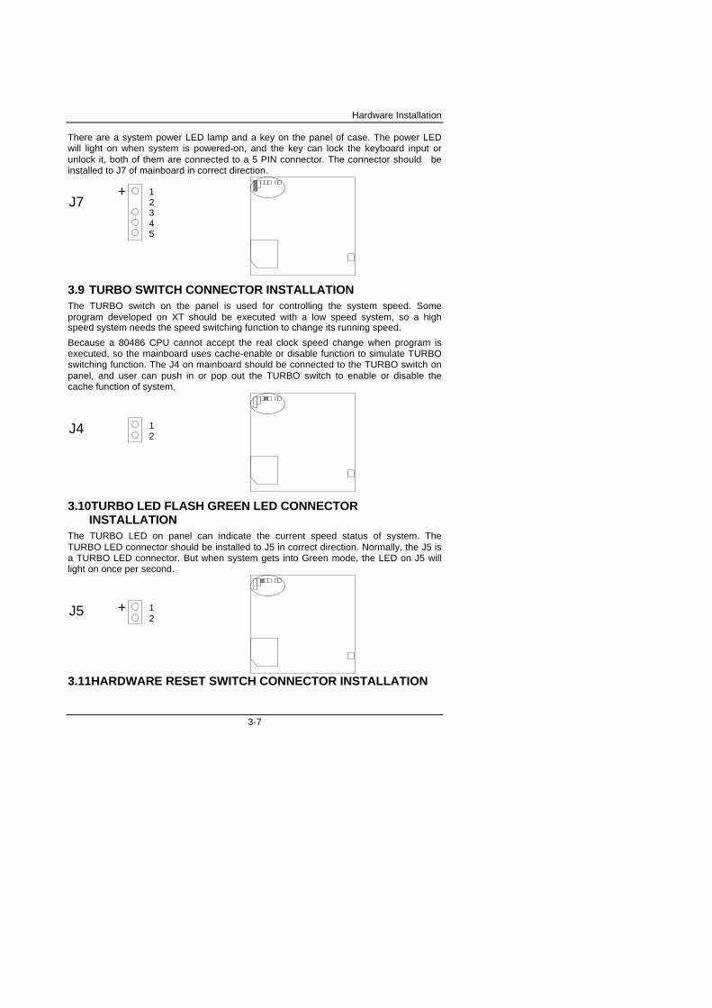
There are a system power LED lamp and a key on the panel of case. The power LEDwill light on when system is powered-on, and the key can lock the keyboard input orunlock it, both of them are connected to a 5 PIN connector. The connector should beinstalled to J7 of mainboard in correct direction.
J7+ 1
2345
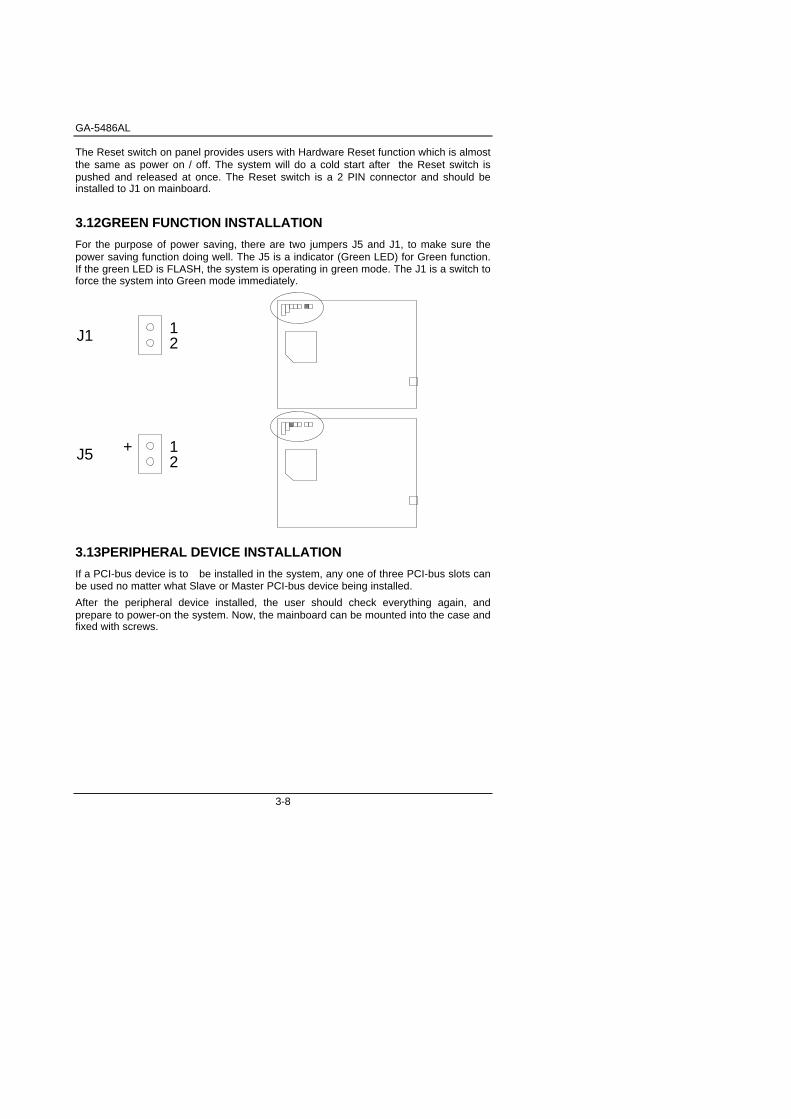
3.9 TURBO SWITCH CONNECTOR INSTALLATIONThe TURBO switch on the panel is used for controlling the system speed. Someprogram developed on XT should be executed with a low speed system, so a highspeed system needs the speed switching function to change its running speed.
Because a 80486 CPU cannot accept the real clock speed change when program isexecuted, so the mainboard uses cache-enable or disable function to simulate TURBOswitching function. The J4 on mainboard should be connected to the TURBO switch onpanel, and user can push in or pop out the TURBO switch to enable or disable thecache function of system.
J4 12
3.10TURBO LED FLASH GREEN LED CONNECTORINSTALLATION
The TURBO LED on panel can indicate the current speed status of system. TheTURBO LED connector should be installed to J5 in correct direction. Normally, the J5 isa TURBO LED connector. But when system gets into Green mode, the LED on J5 willlight on once per second.
J5 12
+
3.11HARDWARE RESET SWITCH CONNECTOR INSTALLATION
GA-5486AL
3-8
The Reset switch on panel provides users with Hardware Reset function which is almostthe same as power on / off. The system will do a cold start after the Reset switch ispushed and released at once. The Reset switch is a 2 PIN connector and should beinstalled to J1 on mainboard.
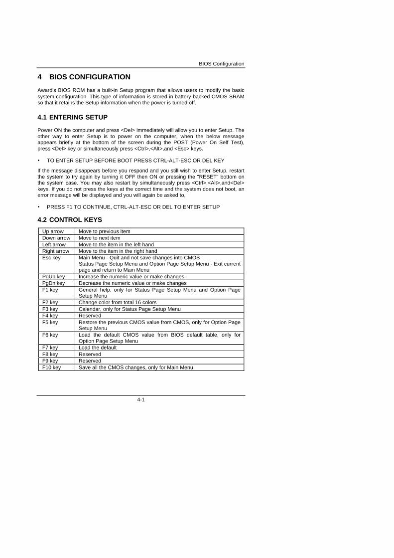
3.12GREEN FUNCTION INSTALLATION
For the purpose of power saving, there are two jumpers J5 and J1, to make sure thepower saving function doing well. The J5 is a indicator (Green LED) for Green function.If the green LED is FLASH, the system is operating in green mode. The J1 is a switch toforce the system into Green mode immediately.
J1 12
J5 12
+
3.13PERIPHERAL DEVICE INSTALLATION
If a PCI-bus device is to be installed in the system, any one of three PCI-bus slots canbe used no matter what Slave or Master PCI-bus device being installed.
After the peripheral device installed, the user should check everything again, andprepare to power-on the system. Now, the mainboard can be mounted into the case andfixed with screws.
BIOS Configuration
4-1
4 BIOS CONFIGURATION
Award's BIOS ROM has a built-in Setup program that allows users to modify the basicsystem configuration. This type of information is stored in battery-backed CMOS SRAMso that it retains the Setup information when the power is turned off.
4.1 ENTERING SETUP
Power ON the computer and press <Del> immediately will allow you to enter Setup. Theother way to enter Setup is to power on the computer, when the below messageappears briefly at the bottom of the screen during the POST (Power On Self Test),press <Del> key or simultaneously press <Ctrl>,<Alt>,and <Esc> keys.
• TO ENTER SETUP BEFORE BOOT PRESS CTRL-ALT-ESC OR DEL KEY
If the message disappears before you respond and you still wish to enter Setup, restartthe system to try again by turning it OFF then ON or pressing the "RESET" bottom onthe system case. You may also restart by simultaneously press <Ctrl>,<Alt>,and<Del>keys. If you do not press the keys at the correct time and the system does not boot, anerror message will be displayed and you will again be asked to,
• PRESS F1 TO CONTINUE, CTRL-ALT-ESC OR DEL TO ENTER SETUP
4.2 CONTROL KEYS
Up arrow Move to previous itemDown arrow Move to next itemLeft arrow Move to the item in the left handRight arrow Move to the item in the right handEsc key Main Menu - Quit and not save changes into CMOS
Status Page Setup Menu and Option Page Setup Menu - Exit currentpage and return to Main Menu
PgUp key Increase the numeric value or make changesPgDn key Decrease the numeric value or make changesF1 key General help, only for Status Page Setup Menu and Option Page
Setup MenuF2 key Change color from total 16 colorsF3 key Calendar, only for Status Page Setup MenuF4 key ReservedF5 key Restore the previous CMOS value from CMOS, only for Option Page
Setup MenuF6 key Load the default CMOS value from BIOS default table, only for
Option Page Setup MenuF7 key Load the defaultF8 key ReservedF9 key ReservedF10 key Save all the CMOS changes, only for Main Menu
GA-5486AL
4-2
4.3 GETTING HELP
4.3.1Main Menu
The on-line description of the highlighted setup function is displayed at the bottom of thescreen.
4.3.2Status Page Setup Menu / Option Page Setup Menu
Press F1 to pop up a small help window that describes the appropriate keys to use andthe possible selections for the highlight item. To exit the Help Window press <Esc>.
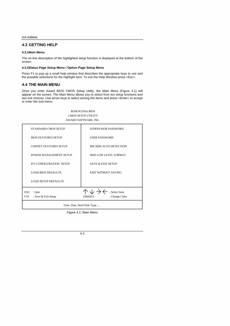
4.4 THE MAIN MENU
Once you enter Award BIOS CMOS Setup Utility, the Main Menu (Figure 4.1) willappear on the screen. The Main Menu allows you to select from ten setup functions andtwo exit choices. Use arrow keys to select among the items and press <Enter> to acceptor enter the sub-menu.
ROM PCI/ISA BIOS
CMOS SETUP UTILITY
AWARD SOFTWARE, INC.
STANDARD CMOS SETUP
BIOS FEATURES SETUP
CHIPSET FEATURES SETUP
POWER MANAGEMENT SETUP
USER PASSWORD
IDE HDD AUTO DETECTION
SAVE & EXIT SETUP
EXIT WITHOUT SAVING
ESC
F10
: Quit
: Save & Exit Setup (Shift)F2
: Select Item
: Change Color
Time, Date, Hard Disk Type ...
LOAD BIOS DEFAULTS
PCI CONFIGURATION SETUP
LOAD SETUP DEFAULTS
SUPERVISOR PASSWORD
HDD LOW LEVEL FORMAT
Figure 4.1: Main Menu
BIOS Configuration
4-3
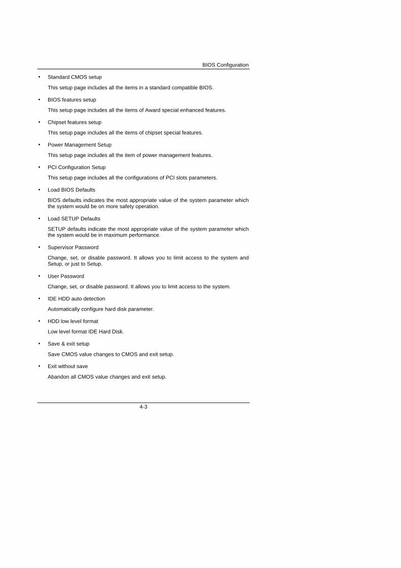
• Standard CMOS setup
This setup page includes all the items in a standard compatible BIOS.
• BIOS features setup
This setup page includes all the items of Award special enhanced features.
• Chipset features setup
This setup page includes all the items of chipset special features.
• Power Management Setup
This setup page includes all the item of power management features.
• PCI Configuration Setup
This setup page includes all the configurations of PCI slots parameters.
• Load BIOS Defaults
BIOS defaults indicates the most appropriate value of the system parameter whichthe system would be on more safety operation.
• Load SETUP Defaults
SETUP defaults indicate the most appropriate value of the system parameter whichthe system would be in maximum performance.
• Supervisor Password
Change, set, or disable password. It allows you to limit access to the system andSetup, or just to Setup.
• User Password
Change, set, or disable password. It allows you to limit access to the system.
• IDE HDD auto detection
Automatically configure hard disk parameter.
• HDD low level format
Low level format IDE Hard Disk.
• Save & exit setup
Save CMOS value changes to CMOS and exit setup.
• Exit without save
Abandon all CMOS value changes and exit setup.
GA-5486AL
4-4
4.5 STANDARD CMOS SETUP MENU
The items in Standard CMOS Setup Menu (Figure 4.2) are divided into 11 categories.Each category includes none, one or more than one setup items. Use the arrows tohighlight the item and then use the <PgUp> or <PgDn> keys to select the value youwant in each item.
ROM PCI/ ISA BIOS
STANDARD CMOS SETUP
AWARD SOFTWARE, INC.
ESC
F1
: Quit
: Help (Shift)F2
: Select Item
: Change Color
Date (mm:dd:yy)
Time (hh:mm:ss)
Primary Master
Drive A
Drive B
Video
Halt On : No Errors
: EGA/VGA
: 1.44 M, 3.5 in.
: NonePrimary Slave
CYLS HEAD PRECOMP LANDZ SECTOR
Base Memory:
Other Memory:
Extended Memory:
Total Memory:
7168 K
640 K
384 K
8192 K
PU/PD/+/- : Modify
: Fri,
: 16 : 12 : 00
MODE
------------- 0
Oct 20 1995
HARD DISKS TYPE SIZE
Second Master
Second Slave
------------- 0
------------- 0
0
0
0
0
0 0
0
0
0
------------- 0
0
0
0
0
0
0
0
0
0
0
0
: None
: None
: None
: None
Figure 4.2: STANDARD CMOS SETUP
• Date
The date format is <day>, <date> <month> <year>.
Press <F3> to show the calendar.
day The day, from Sun to Sat, determined by
the BIOS and is display-only
dat
e
The date, from 1 to 31 (or the maximum
allowed in the month)
mon
th
The month, Jan. through Dec.

BIOS Configuration
4-5
yea
r
The year, from 1900 through 2099
• Time
The time format in <hour> <minute> <second>. The
time is calculated base on the 24-hour military-
time clock. For example, 1 p.m. is 13:00:00.

GA-5486AL
4-6
• Primary Master / Slave, Secondary Master / Salve
The category identify the types of hard disk
drive C or drive F 4 devices that has been
installed in the computer. There are 46 pre-
defined types and a user definable type. Type 1
to Type 46 are pre-defined. Type User is user-
definable.
Press PgUp or PgDn to select a numbered hard disk
type or type the number and press <Enter>. Note
that the specifications of your drive must match
with the drive table. The hard disk will not work
properly if you enter improper information for
this category. If your hard disk drive type is
not matched or listed, you can use Type User to
define your own drive type manually.
If you select Type User, related information is
asked to be entered to the following items. Enter
the information directly from the keyboard and
press <Enter>. Those information should be
provided in the documentation form your hard disk
vendor or the system manufacturer.
CYLS. number of cylinders
HEADS number of heads
PRECOMP write precom
LANDZON
E
landing zone
SECTORS number of sectors
BIOS Configuration
4-7
If a hard disk has not been installed select NONE
and press <Enter>.
• Drive A type / Drive B type
The category identify the types of floppy disk
drive A or drive B that has been installed in the
computer.
None No floppy drive installed
360K,
5.25 in.
5-1/4 inch PC-type double-sided
drive; 360 kilobyte capacity
1.2M,
5.25 in.
5-1/4 inch AT-type double-sided and
high-density drive; 1.2 megabyte
capacity
720K,
3.5 in.
3-1/2 inch double-sided drive; 720
kilobyte capacity
1.44M,
3.5 in.
3-1/2 inch double-sided and high-
density drive; 1.44 megabyte capacity
2.88M,
3.5 in.
3-1/2 inch double-sided drive; 2.88
megabyte capacity
• Video
The category detects the type of adapter used for
the primary system monitor that must match your
video display card and monitor. Although
secondary monitors are supported, you do not have
to select the type in setup.
EGA/VG
A
Enhanced Graphics Adapter/Video
Graphics Array. For EGA, VGA, SVGA, or
PGA monitor adapters

GA-5486AL
4-8
CGA 40 Color Graphics Adapter, power up in 40
column mode
CGA 80 Color Graphics Adapter, power up in 80
column mode
MONO Monochrome adapter, includes high
resolution monochrome adapters
BIOS Configuration
4-9
• Halt on
The category determines whether the computer will
stop if an error is detected during power up.
No errors Whenever the BIOS detects a non-
fatal error the system will not
stop and you will be prompted
All errors The system boot will stop for any
error that may be detected
All, But
Keyboard
The system boot will not stop for
a keyboard error; it will stop for
all other errors
All, But
Diskette
The system boot will not stop for
a disk error; it will stop for all
other errors
All, But
Disk/Key
The system boot will not stop for
a keyboard or disk error; it will
stop for all other errors
• Memory
The category is display-only which is determined
by POST (Power On Self Test) of the BIOS.
Base Memory
The POST of the BIOS will determine the amount
of base (or conventional) memory installed in
the system. The value of the base memory is
typically 512 K for systems with 512 K memory
installed on the motherboard, or 640 K for
GA-5486AL
4-10
systems with 640 K or more memory installed on
the motherboard.
Extended Memory
The BIOS determines how much extended memory is
presented during the POST. This is the amount
of memory located above 1 MB in the CPU's
memory address map.
Expanded Memory
Expanded Memory in memory defined by the
Lotus/Intel/Microsoft (LIM) standard as EMS.
Many standard DOS applications can not utilize
memory above 64KB, the Expanded Memory
Specification (EMS) swaps memory which is not
utilized by DOS with a section, or frame, so
these applications can access to all of the
system memory. Memory can be swapped by EMS is
usually 64KB within 1 MB or memory above 1 MB,
depending on the chipset design.
Expanded memory device driver is required to
use memory as Expanded Memory.
Other Memory
This refers to the memory located in the 640KB
to 1024KB address space. This is the memory
that can be used for different applications.
DOS uses this area to load device drivers to
keep as much base memory free for application
programs. Most use for this area is Shadow RAM.
BIOS Configuration
4-11
4.6 BIOS FEATURES SETUPROM PCI/ISA BIOS
BIOS FEATURES SETUP
AWARD SOFTWARE, INC.
: Select Item
Virus Warning
External Cache
Boot Sequence
Boot Up Floppy Seek
Boot Up NumLock Status
Security Option
Video BIOS Shadow
D0000 - D7FFF Shadow
: Off
: Setup
: Disabled
: Enabled
: Enabled
: Enabled
: A, C
: Enabled
: Disabled
: Disabled
: Disabled
ESC
F1
F5
F6
F7 : Load Setup Defaults
: Quit
: Help
: Old Values
: Load BIOS Defaults
PU/PD/+/-
(Shift)F2
: Modify
: Color
Quick Power On Self Test : Enabled
Swap Floppy Drive : Disabled
PCI/VGA & ISA/MPEG INSTALL
C8000 - CFFFF Shadow
D8000 - DFFFF Shadow
: Disabled
Boot Up System Speed : High
CPU Internal Cache
Figure 4.3: BIOS FEATURES SETUP
• Virus Warning
This category flashes on the screen. During and after the system boots up, anyattempt to write to the boot sector or partition table of the hard disk drive will halt thesystem and the following error message will appear, in the mean time, you can runanti-virus program to locate the problem. The default value is Disabled.
Enabled Activate automatically when the system boots up and causes awarning message to appear when anything attempts to access tothe boot sector or hard disk partition table.
Disabled No warning message to appear when anything attempts to accessto the boot sector or hard disk partition table.
• CPU Internal Cache / External Cache
These two categories speed up memory access. However, it depends on CPU /chipset design. The default value is Enabled.
Enabled Enable cache.Disabled Disable cache.
GA-5486AL
4-12
• Quick Power On Self Test
This category speeds up Power On Self Test (POST) after you power on thecomputer. If it is set to Enable, BIOS will shorten or skip some check items duringPOST. The default value is Enabled.
Enabled Enable quick POST.Disabled Normal POST.
• Boot Sequence
This category determines which drive computer searches first for the disk operatingsystem (i.e., DOS). The default value is A,C.
A,C System will first search for floppy disk drive and then hard disk drive.C,A System will first search for hard disk drive and then floppy disk drive.
• Swap Floppy Drive
The default value is Disabled.
Enabled Floppy A & B will be swapped under DOS.Disabled Floppy A & B will be normal definition.
• Boot Up Floppy Seek
During POST, BIOS will determine if the floppy disk drive installed is 40 or 80 tracks.360 type is 40 tracks while 720,1.2 and 1.44 are all 80 tracks.The default value is Enabled.
Enabled BIOS searches for floppy disk drive to determine if it is 40 or 80tracks, Note that BIOS cannot tell from 720, 1.2 or 1.44 drive typeas they are all 80 tracks.
Disabled BIOS will not search for the type of floppy disk drive by tracknumber. Note that there will not be any warning message if thedriver installed is 360.
• Boot Up NumLock Status
The default value is Off.
On Keypad is number keys.Off Keypad is arrow keys.
• Boot Up System Speed
The default value is High.
High CPU input clock depends on the setting of JP7 (CPU input clockjumper).
Low CPU input clock is fixed on 33 MHz.
• Security Option
The default value is Setup.
Setup Asking password when enter CMOS Setup.System Asking password when enter CMOS Setup and boot system.
• PCI/VGA & ISA/MPEG Install
BIOS Configuration
4-13
The default value is Disabled.
Enabled Enable PCI/VGA & ISA/MPEG Install.Disabled Disable PCI/VGA & ISA/MPEG Install.
• C8000 - CFFFF Shadow / D0000 - DFFFF Shadow
These categories determine whether optional ROM will be copied to RAM by 16Kbyte. The default value are Disabled.
Enabled Optional shadow is enabled.Disabled Optional shadow is disabled.
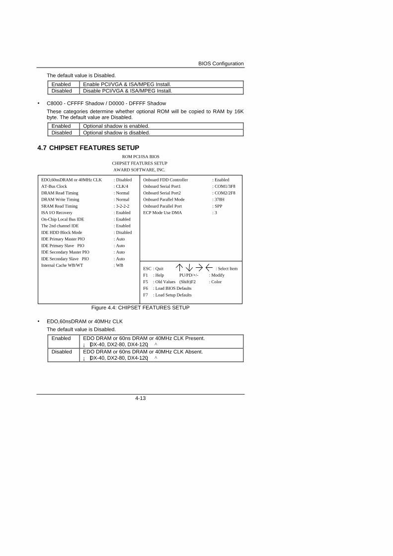
4.7 CHIPSET FEATURES SETUPROM PCI/ISA BIOS
CHIPSET FEATURES SETUP
AWARD SOFTWARE, INC.
: Select Item
EDO,60nsDRAM or 40MHz CLK : Disabled
: Disabled
ESC
F1
F5
F6
F7 : Load Setup Defaults
: Quit
: Help
: Old Values
: Load BIOS Defaults
PU/PD/+/-
(Shift)F2
: Modify
: Color
: Normal
AT-Bus Clock
DRAM Read Timing
ISA I/O Recovery
IDE HDD Block Mode
: 3-2-2-2
The 2nd channel IDE
DRAM Write Timing
On-Chip Local Bus IDE : Enabled
: Auto
Onboard FDD Controller
Onboard Parallel Mode
Onboard Parallel Port
Onboard Serial Port1
Onboard Serial Port2
: Enabled
: SPP
: 378H
: COM1/3F8
: COM2/2F8
SRAM Read Timing
IDE Primary Master PIO
IDE Primary Slave PIO
IDE Secondary Master PIO
IDE Secondary Slave PIO
: Normal
: Enabled
: Enabled
: Auto
: Auto
: Auto
Internal Cache WB/WT : WB
ECP Mode Use DMA : 3
: CLK/4
Figure 4.4: CHIPSET FEATURES SETUP
• EDO,60nsDRAM or 40MHz CLK
The default value is Disabled.
Enabled EDO DRAM or 60ns DRAM or 40MHz CLK Present.¡ ]DX-40, DX2-80, DX4-120¡ ^
Disabled EDO DRAM or 60ns DRAM or 40MHz CLK Absent.¡ ]DX-40, DX2-80, DX4-120¡ ^
GA-5486AL
4-14
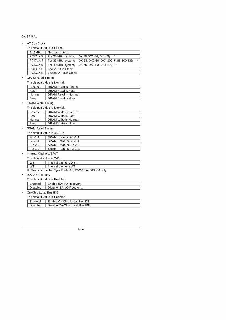
• AT Bus Clock
The default value is CLK/4.
7.19MHz Normal setting.PCICLK/3 For 25 MHz system.¡ ]DX-25,DX2-50, DX4-75¡ ^
PCICLK/4 For 33 MHz system.¡ ]DX-33, DX2-66, DX4-100, 5x86-100/133¡ ^
PCICLK/5 For 40 MHz system.¡ ]DX-40, DX2-80, DX4-120¡ ^
PCICLK/6 Low AT Bus Clock.PCICLK/8 Lowest AT Bus Clock.
• DRAM Read Timing
The default value is Normal.
Fastest DRAM Read is Fastest.Fast DRAM Read is Fast.Normal DRAM Read is Normal.Slow DRAM Read is slow.
• DRAM Write Timing
The default value is Normal.
Fastest DRAM Write is Fastest.Fast DRAM Write is Fast.Normal DRAM Write is Normal.Slow DRAM Write is slow.
• SRAM Read Timing
The default value is 3-2-2-2.
2-1-1-1 SRAM read is 2-1-1-1.3-1-1-1 SRAM read is 3-1-1-1.3-2-2-2 SRAM read is 3-2-2-2.4-2-2-2 SRAM read is 4-2-2-2.
• Internal Cache WB/WT
The default value is WB.
WB Internal cache is WB.WT Internal cache is WT.¯ This option is for Cyrix DX4-100, DX2-80 or DX2-66 only.
• ISA I/O Recovery
The default value is Enabled.
Enabled Enable ISA I/O Recovery.Disabled Disable ISA I/O Recovery.
• On-Chip Local Bus IDE
The default value is Enabled.
Enabled Enable On-Chip Local Bus IDE.Disabled Disable On-Chip Local Bus IDE.
BIOS Configuration
4-15
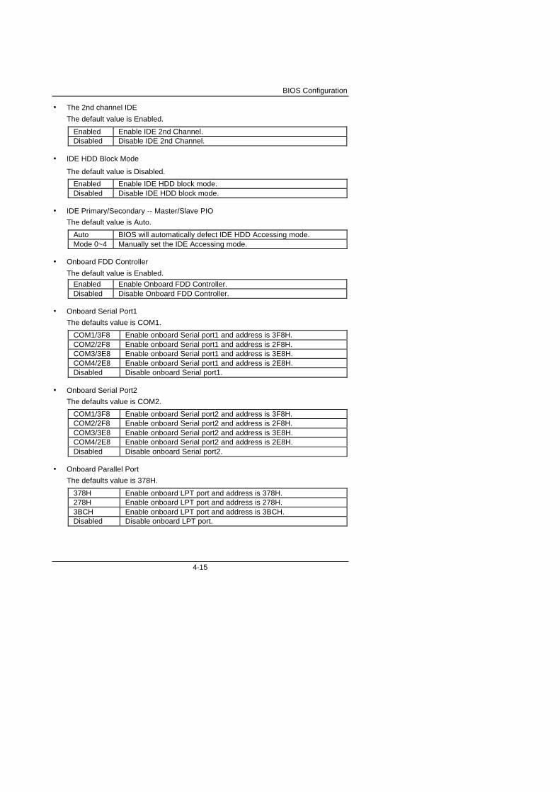
• The 2nd channel IDE
The default value is Enabled.
Enabled Enable IDE 2nd Channel.Disabled Disable IDE 2nd Channel.
• IDE HDD Block Mode
The default value is Disabled.
Enabled Enable IDE HDD block mode.Disabled Disable IDE HDD block mode.
• IDE Primary/Secondary -- Master/Slave PIO
The default value is Auto.
Auto BIOS will automatically defect IDE HDD Accessing mode.Mode 0~4 Manually set the IDE Accessing mode.
• Onboard FDD Controller
The default value is Enabled.
Enabled Enable Onboard FDD Controller.Disabled Disable Onboard FDD Controller.
• Onboard Serial Port1
The defaults value is COM1.
COM1/3F8 Enable onboard Serial port1 and address is 3F8H.COM2/2F8 Enable onboard Serial port1 and address is 2F8H.COM3/3E8 Enable onboard Serial port1 and address is 3E8H.COM4/2E8 Enable onboard Serial port1 and address is 2E8H.Disabled Disable onboard Serial port1.
• Onboard Serial Port2
The defaults value is COM2.
COM1/3F8 Enable onboard Serial port2 and address is 3F8H.COM2/2F8 Enable onboard Serial port2 and address is 2F8H.COM3/3E8 Enable onboard Serial port2 and address is 3E8H.COM4/2E8 Enable onboard Serial port2 and address is 2E8H.Disabled Disable onboard Serial port2.
• Onboard Parallel Port
The defaults value is 378H.
378H Enable onboard LPT port and address is 378H.278H Enable onboard LPT port and address is 278H.3BCH Enable onboard LPT port and address is 3BCH.Disabled Disable onboard LPT port.
GA-5486AL
4-16
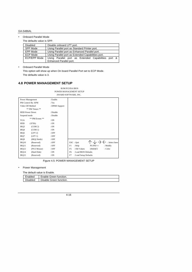
• Onboard Parallel Mode
The defaults value is SPP.
Disabled Disable onboard LPT port.SPP Mode Using Parallel port as Standard Printer port.EPP Mode Using Parallel port as Enhanced Parallel port.ECP Mode Using Parallel port as Extended Capabilities port.ECP/EPP Mode Using Parallel port as Extended Capabilities port &
Enhanced Parallel port.
• Onboard Parallel Mode
This option will show up when On board Parallel Port set to ECP Mode.
The defaults value is 3.
4.8 POWER MANAGEMENT SETUPROM PCI/ISA BIOS
POWER MANAGEMENT SETUP
AWARD SOFTWARE, INC.
: Select ItemESC
F1
F5
F6
F7 : Load Setup Defaults
: Quit
: Help
: Old Values
: Load BIOS Defaults
PU/PD/+/-
(Shift)F2
: Modify
: Color
Power Management : Enable
: Disable
Video Off Method
HDD Power Down
** PM Timers **
: Yes
** PM Events **: ONVGA
IRQ3
PM Control By APM
Suspend mode
: DPMS Support
IRQ4
IRQ5
IRQ7
IRQ9
IRQ10
IRQ11
IRQ12
IRQ14
IRQ15
(1FXh)
(COM 2)
(COM 1)
(IRQ2 Redir)
(Reserved)
(Hard Disk)
(LPT 2)
(LPT 1)
(Reserved)
HDD
(PS/2 Mouse)
(Reserved)
: ON
: ON
: ON
: OFF
: ON
: ON
: OFF
: OFF
: OFF
: OFF
: OFF
: Disable
Figure 4.5: POWER MANAGEMENT SETUP
• Power Management
The default value is Enable.
Enabled Enable Green function.Disabled Disable Green function.
BIOS Configuration
4-17
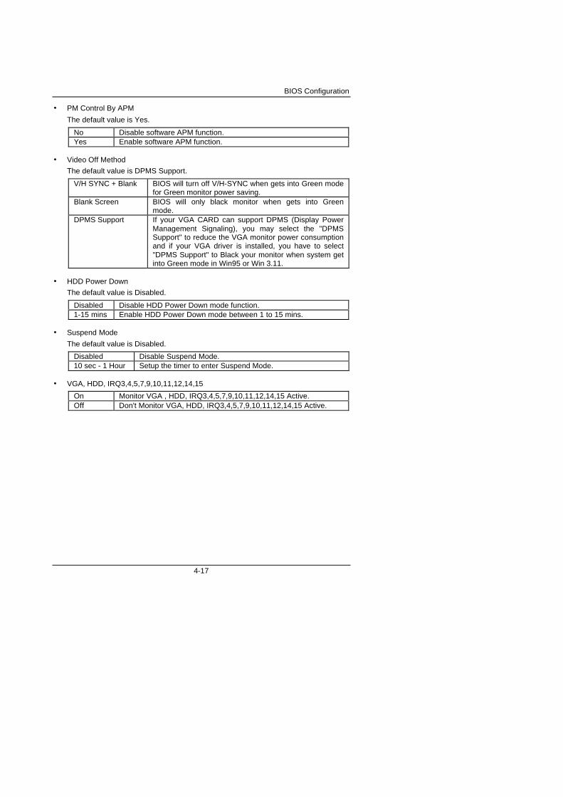
• PM Control By APM
The default value is Yes.
No Disable software APM function.Yes Enable software APM function.
• Video Off Method
The default value is DPMS Support.
V/H SYNC + Blank BIOS will turn off V/H-SYNC when gets into Green modefor Green monitor power saving.
Blank Screen BIOS will only black monitor when gets into Greenmode.
DPMS Support If your VGA CARD can support DPMS (Display PowerManagement Signaling), you may select the "DPMSSupport" to reduce the VGA monitor power consumptionand if your VGA driver is installed, you have to select"DPMS Support" to Black your monitor when system getinto Green mode in Win95 or Win 3.11.
• HDD Power Down
The default value is Disabled.
Disabled Disable HDD Power Down mode function.1-15 mins Enable HDD Power Down mode between 1 to 15 mins.
• Suspend Mode
The default value is Disabled.
Disabled Disable Suspend Mode.10 sec - 1 Hour Setup the timer to enter Suspend Mode.
• VGA, HDD, IRQ3,4,5,7,9,10,11,12,14,15
On Monitor VGA , HDD, IRQ3,4,5,7,9,10,11,12,14,15 Active.Off Don't Monitor VGA, HDD, IRQ3,4,5,7,9,10,11,12,14,15 Active.
GA-5486AL
4-18
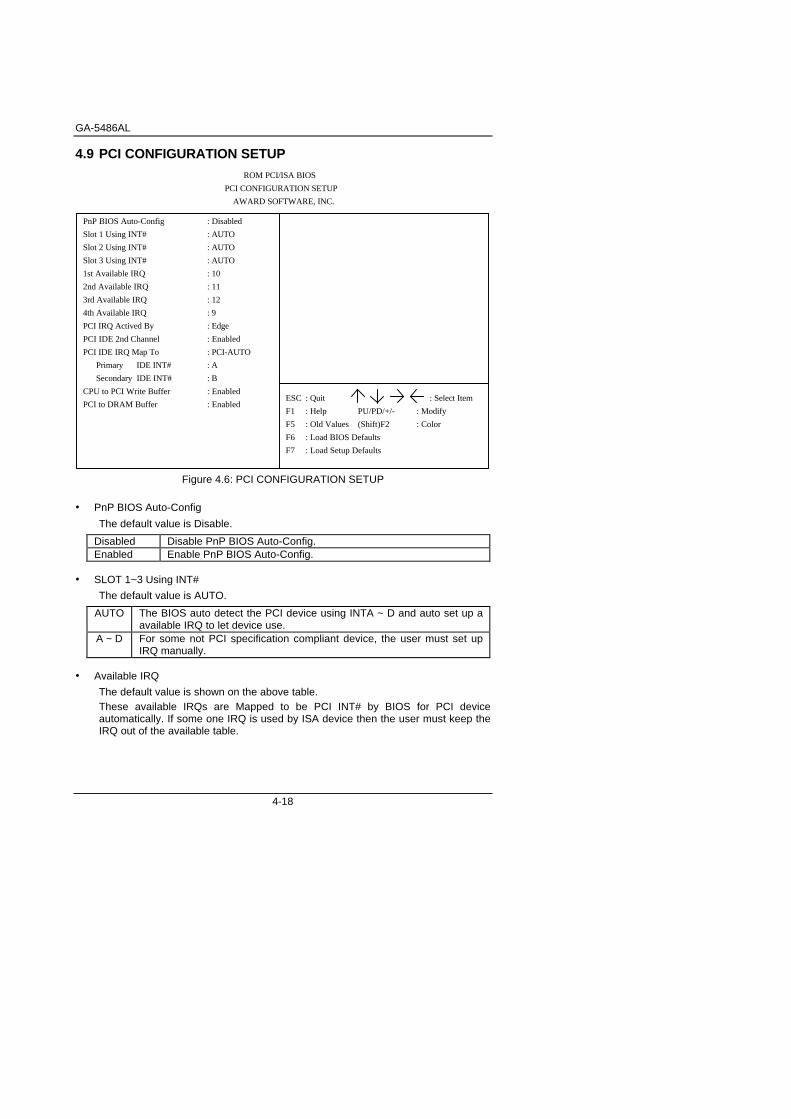
4.9 PCI CONFIGURATION SETUPROM PCI/ISA BIOS
PCI CONFIGURATION SETUP
AWARD SOFTWARE, INC.
: Select ItemESC
F1
F5
F6
F7 : Load Setup Defaults
: Quit
: Help
: Old Values
: Load BIOS Defaults
PU/PD/+/-
(Shift)F2
: Modify
: Color
Slot 1 Using INT# : AUTO
: 9
Slot 2 Using INT#
Slot 3 Using INT#
1st Available IRQ
: 11
: 12
: 10
: AUTO
: AUTO
2nd Available IRQ
3rd Available IRQ
4th Available IRQ
PCI IDE 2nd Channel : Enabled
PCI IRQ Actived By : Edge
: DisabledPnP BIOS Auto-Config
: PCI-AUTOPCI IDE IRQ Map To
Secondary IDE INT# : B
Primary IDE INT# : A
CPU to PCI Write Buffer
PCI to DRAM Buffer : Enabled
: Enabled
Figure 4.6: PCI CONFIGURATION SETUP
• PnP BIOS Auto-Config
The default value is Disable.
Disabled Disable PnP BIOS Auto-Config.Enabled Enable PnP BIOS Auto-Config.
• SLOT 1~3 Using INT#
The default value is AUTO.
AUTO The BIOS auto detect the PCI device using INTA ~ D and auto set up aavailable IRQ to let device use.
A ~ D For some not PCI specification compliant device, the user must set upIRQ manually.
• Available IRQ
The default value is shown on the above table.These available IRQs are Mapped to be PCI INT# by BIOS for PCI deviceautomatically. If some one IRQ is used by ISA device then the user must keep theIRQ out of the available table.
BIOS Configuration
4-19
• PCI IRQ Actived By
The default value is Edge.
Edge Normal Operation.Level For some PCI SCSI or Lan device using same PCI INT.
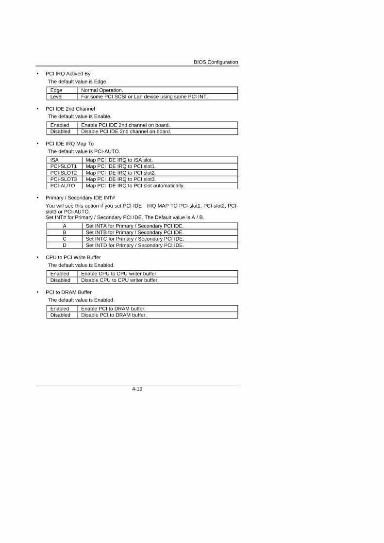
• PCI IDE 2nd Channel
The default value is Enable.
Enabled Enable PCI IDE 2nd channel on board.Disabled Disable PCI IDE 2nd channel on board.
• PCI IDE IRQ Map To
The default value is PCI-AUTO.
ISA Map PCI IDE IRQ to ISA slot.PCI-SLOT1 Map PCI IDE IRQ to PCI slot1.PCI-SLOT2 Map PCI IDE IRQ to PCI slot2.PCI-SLOT3 Map PCI IDE IRQ to PCI slot3.PCI-AUTO Map PCI IDE IRQ to PCI slot automatically.
• Primary / Secondary IDE INT#
You will see this option if you set PCI IDE IRQ MAP TO PCI-slot1, PCI-slot2, PCI-slot3 or PCI-AUTO.Set INT# for Primary / Secondary PCI IDE. The Default value is A / B.
A Set INTA for Primary / Secondary PCI IDE.B Set INTB for Primary / Secondary PCI IDE.C Set INTC for Primary / Secondary PCI IDE.D Set INTD for Primary / Secondary PCI IDE.
• CPU to PCI Write Buffer
The default value is Enabled.
Enabled Enable CPU to CPU writer buffer.Disabled Disable CPU to CPU writer buffer.
• PCI to DRAM Buffer
The default value is Enabled.
Enabled Enable PCI to DRAM buffer.Disabled Disable PCI to DRAM buffer.
GA-5486AL
4-20
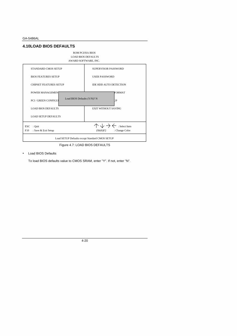
4.10LOAD BIOS DEFAULTS
HDD LOW LEVEL FORMAT
SAVE & EXIT SETUP
POWER MANAGEMENT
LOAD BIOS DEFAULTS
PCI / GREEN CONFIGURATION SETUP
ROM PCI/ISA BIOS
LOAD BIOS DEFAULTS
AWARD SOFTWARE, INC.
STANDARD CMOS SETUP
BIOS FEATURES SETUP
CHIPSET FEATURES SETUP
USER PASSWORD
IDE HDD AUTO DETECTION
EXIT WITHOUT SAVING
ESC
F10
: Quit
: Save & Exit Setup (Shift)F2
: Select Item
: Change Color
Load BIOS Defaults (Y/N)? N
Load SETUP Defaults except Standard CMOS SETUP
LOAD SETUP DEFAULTS
SUPERVISOR PASSWORD
Figure 4.7: LOAD BIOS DEFAULTS
• Load BIOS Defaults
To load BIOS defaults value to CMOS SRAM, enter "Y". If not, enter "N".
BIOS Configuration
4-21
4.11LOAD SETUP DEFAULTS
HDD LOW LEVEL FORMAT
PCI CONFIGURATION SETUP
ROM PCI/ISA BIOS
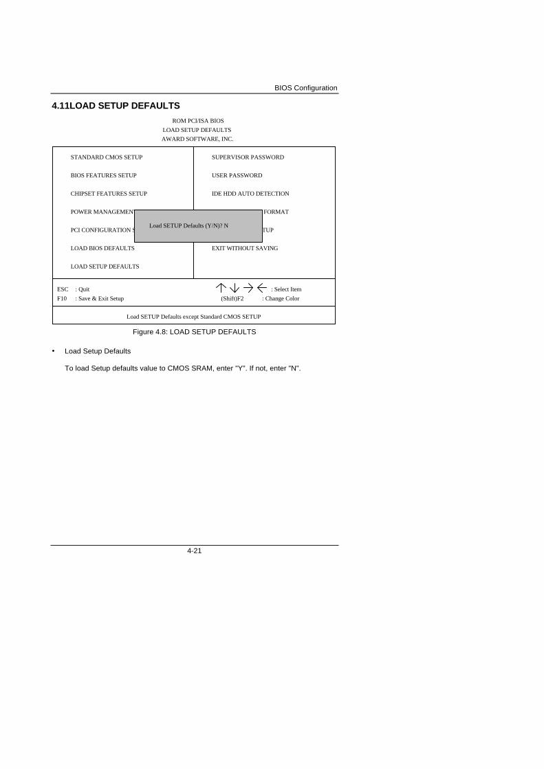
LOAD SETUP DEFAULTS
AWARD SOFTWARE, INC.
STANDARD CMOS SETUP
BIOS FEATURES SETUP
CHIPSET FEATURES SETUP
POWER MANAGEMENT
SUPERVISOR PASSWORD
IDE HDD AUTO DETECTION
SAVE & EXIT SETUP
EXIT WITHOUT SAVING
ESC
F10
: Quit
: Save & Exit Setup (Shift)F2
: Select Item
: Change Color
Load SETUP Defaults (Y/N)? N
Load SETUP Defaults except Standard CMOS SETUP
LOAD BIOS DEFAULTS
LOAD SETUP DEFAULTS
USER PASSWORD
Figure 4.8: LOAD SETUP DEFAULTS
• Load Setup Defaults
To load Setup defaults value to CMOS SRAM, enter "Y". If not, enter "N".
GA-5486AL
4-22
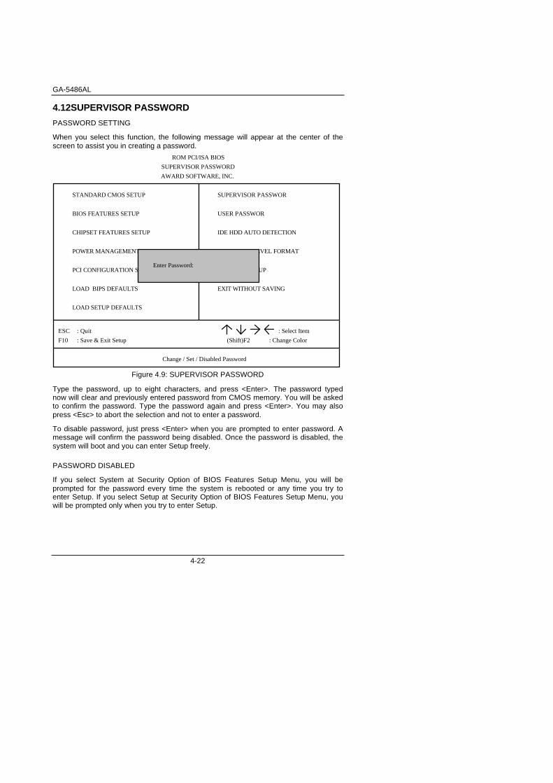
4.12SUPERVISOR PASSWORD
PASSWORD SETTING
When you select this function, the following message will appear at the center of thescreen to assist you in creating a password.
HDD LOW LEVEL FORMAT
PCI CONFIGURATION SETUP
ROM PCI/ISA BIOS
AWARD SOFTWARE, INC.
STANDARD CMOS SETUP
BIOS FEATURES SETUP
CHIPSET FEATURES SETUP
POWER MANAGEMENT
SUPERVISOR PASSWOR
IDE HDD AUTO DETECTION
SAVE & EXIT SETUP
EXIT WITHOUT SAVING
ESC
F10
: Quit
: Save & Exit Setup (Shift)F2
: Select Item
: Change Color
Enter Password:
Change / Set / Disabled Password
LOAD BIPS DEFAULTS
LOAD SETUP DEFAULTS
SUPERVISOR PASSWORD
USER PASSWOR
Figure 4.9: SUPERVISOR PASSWORD
Type the password, up to eight characters, and press <Enter>. The password typednow will clear and previously entered password from CMOS memory. You will be askedto confirm the password. Type the password again and press <Enter>. You may alsopress <Esc> to abort the selection and not to enter a password.
To disable password, just press <Enter> when you are prompted to enter password. Amessage will confirm the password being disabled. Once the password is disabled, thesystem will boot and you can enter Setup freely.
PASSWORD DISABLED
If you select System at Security Option of BIOS Features Setup Menu, you will beprompted for the password every time the system is rebooted or any time you try toenter Setup. If you select Setup at Security Option of BIOS Features Setup Menu, youwill be prompted only when you try to enter Setup.
BIOS Configuration
4-23
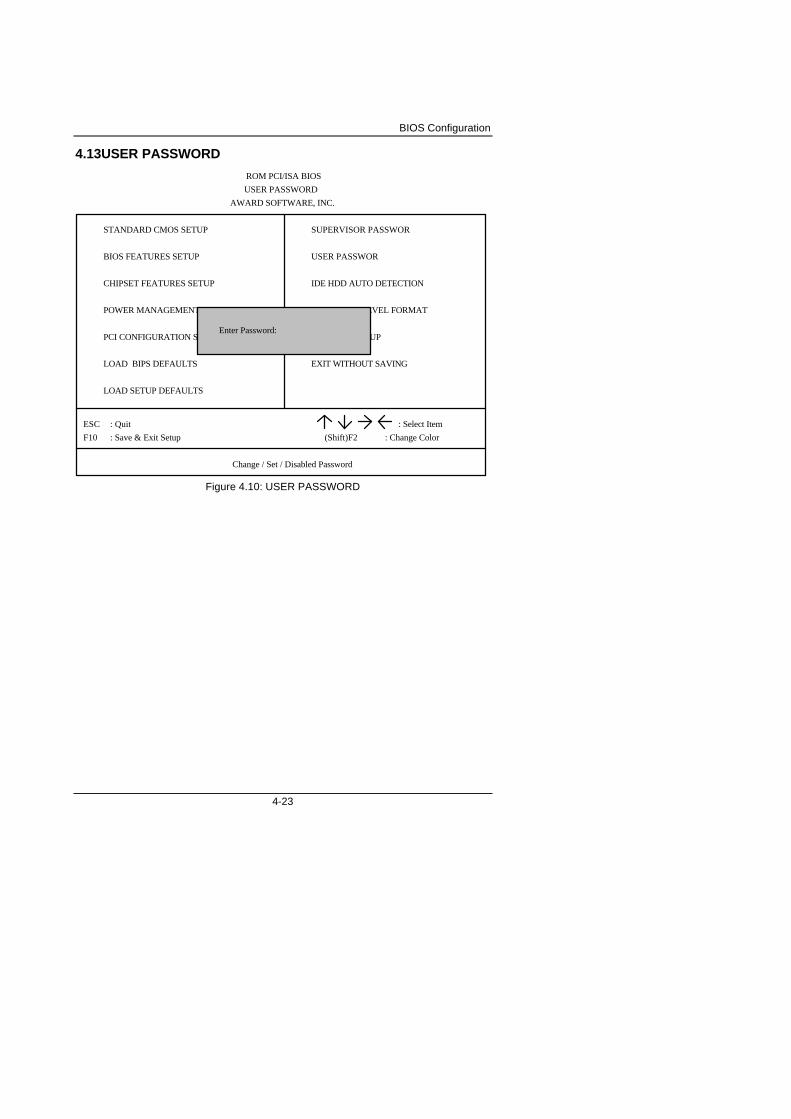
4.13USER PASSWORD
HDD LOW LEVEL FORMAT
PCI CONFIGURATION SETUP
ROM PCI/ISA BIOS
AWARD SOFTWARE, INC.
STANDARD CMOS SETUP
BIOS FEATURES SETUP
CHIPSET FEATURES SETUP
POWER MANAGEMENT
SUPERVISOR PASSWOR
IDE HDD AUTO DETECTION
SAVE & EXIT SETUP
EXIT WITHOUT SAVING
ESC
F10
: Quit
: Save & Exit Setup (Shift)F2
: Select Item
: Change Color
Enter Password:
Change / Set / Disabled Password
LOAD BIPS DEFAULTS
LOAD SETUP DEFAULTS
USER PASSWORD
USER PASSWOR
Figure 4.10: USER PASSWORD
GA-5486AL
4-24
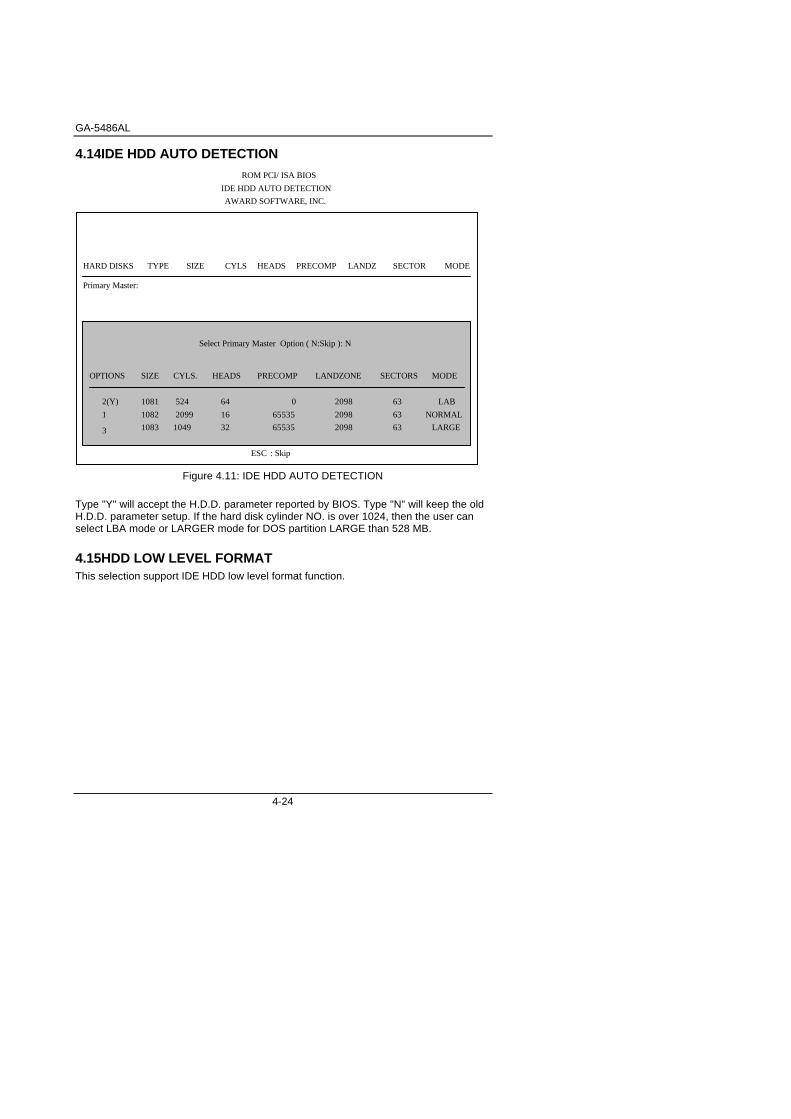
4.14IDE HDD AUTO DETECTIONROM PCI/ ISA BIOS
IDE HDD AUTO DETECTION
AWARD SOFTWARE, INC.
ESC : Skip
Primary Master::
CYLS HEADS PRECOMP LANDZ SECTOR MODE
Select Primary Master Option ( N:Skip ): N
OPTIONS SIZE CYLS. HEADS PRECOMP LANDZONE SECTORS MODE
2(Y)
3
1081
1082
1083
524
2099 16
64
32 2098
65535
65535
0 63
63
63
NORMAL
LAB
LARGE
HARD DISKS TYPE SIZE
1
1049
2098
2098
Figure 4.11: IDE HDD AUTO DETECTION
Type "Y" will accept the H.D.D. parameter reported by BIOS. Type "N" will keep the oldH.D.D. parameter setup. If the hard disk cylinder NO. is over 1024, then the user canselect LBA mode or LARGER mode for DOS partition LARGE than 528 MB.
4.15HDD LOW LEVEL FORMATThis selection support IDE HDD low level format function.
BIOS Configuration
4-25
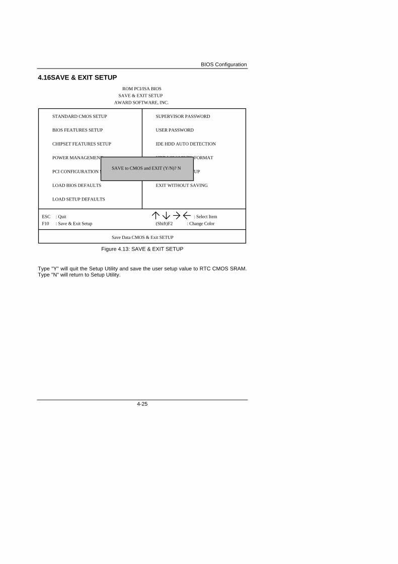
4.16SAVE & EXIT SETUP
HDD LOW LEVEL FORMAT
PCI CONFIGURATION SETUP
ROM PCI/ISA BIOS
SAVE & EXIT SETUP
AWARD SOFTWARE, INC.
STANDARD CMOS SETUP
BIOS FEATURES SETUP
CHIPSET FEATURES SETUP
POWER MANAGEMENT
IDE HDD AUTO DETECTION
SAVE & EXIT SETUP
EXIT WITHOUT SAVING
ESC
F10
: Quit
: Save & Exit Setup (Shift)F2
: Select Item
: Change Color
SAVE to CMOS and EXIT (Y/N)? N
Save Data CMOS & Exit SETUP
LOAD BIOS DEFAULTS
LOAD SETUP DEFAULTS
SUPERVISOR PASSWORD
USER PASSWORD
Figure 4.13: SAVE & EXIT SETUP
Type "Y" will quit the Setup Utility and save the user setup value to RTC CMOS SRAM.Type "N" will return to Setup Utility.
GA-5486AL
4-26
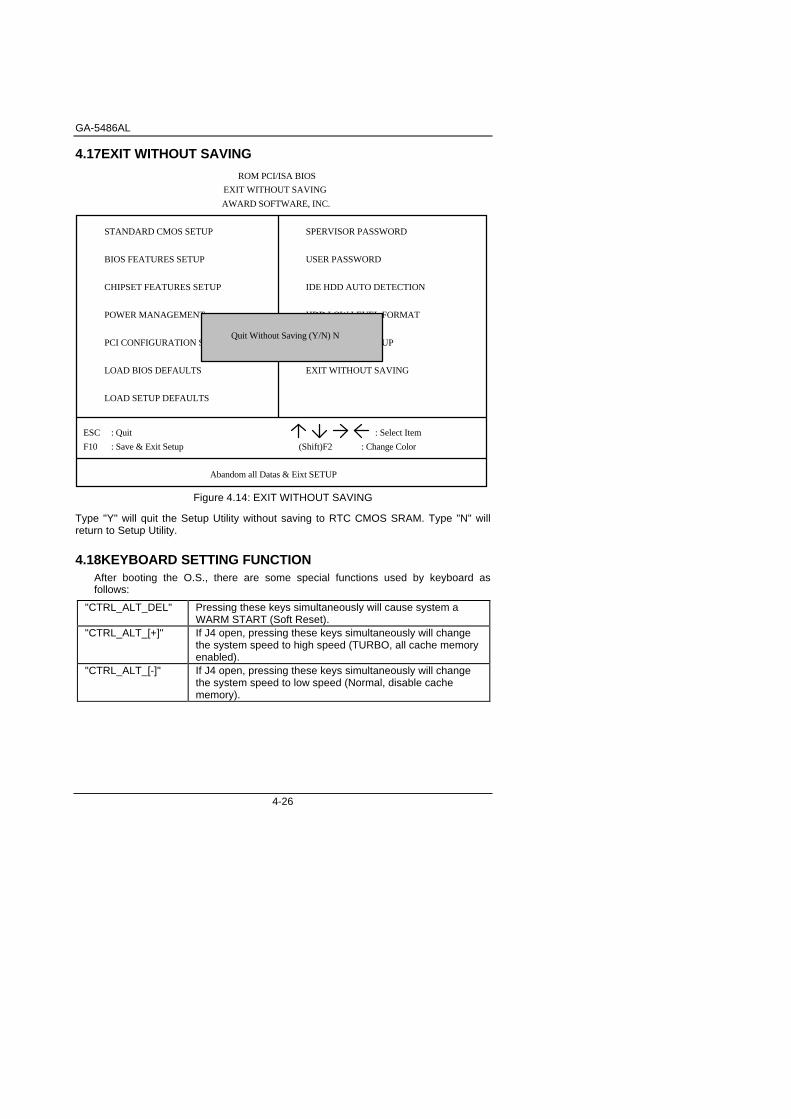
4.17EXIT WITHOUT SAVING
HDD LOW LEVEL FORMAT
PCI CONFIGURATION SETUP
ROM PCI/ISA BIOS
EXIT WITHOUT SAVING
AWARD SOFTWARE, INC.
STANDARD CMOS SETUP
BIOS FEATURES SETUP
CHIPSET FEATURES SETUP
POWER MANAGEMENT
SPERVISOR PASSWORD
IDE HDD AUTO DETECTION
SAVE & EXIT SETUP
EXIT WITHOUT SAVING
ESC
F10
: Quit
: Save & Exit Setup (Shift)F2
: Select Item
: Change Color
Quit Without Saving (Y/N) N
Abandom all Datas & Eixt SETUP
LOAD BIOS DEFAULTS
LOAD SETUP DEFAULTS
USER PASSWORD
Figure 4.14: EXIT WITHOUT SAVING
Type "Y" will quit the Setup Utility without saving to RTC CMOS SRAM. Type "N" willreturn to Setup Utility.
4.18KEYBOARD SETTING FUNCTIONAfter booting the O.S., there are some special functions used by keyboard asfollows:
"CTRL_ALT_DEL" Pressing these keys simultaneously will cause system aWARM START (Soft Reset).
"CTRL_ALT_[+]" If J4 open, pressing these keys simultaneously will changethe system speed to high speed (TURBO, all cache memoryenabled).
"CTRL_ALT_[-]" If J4 open, pressing these keys simultaneously will changethe system speed to low speed (Normal, disable cachememory).
AT Technical Information
5-1
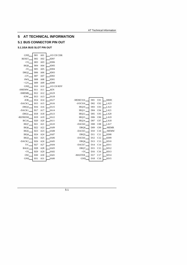
5 AT TECHNICAL INFORMATION
5.1 BUS CONNECTOR PIN OUT
5.1.1ISA BUS SLOT PIN OUT
B23
B24
B31
B05
B07
B10
B13
B15
B19
B21
B25
B29
B02
B04
B08
B11
B14
B17
B20
B26
B27
B01
B03
B06
B09
B12
B16
B18
B22
B28
B30
-REFRESH
A05
A07
A10
A13
A15
A19
A21
A02
A04
A08
A11
A14
A17
A20
A01
A03
A06
A09
A12
A16
A18
A22
A23
A24
A31
A25
A29
A26
A27
A28
A30
D05
D07
D10
D13
D15
D02
D04
D08
D11
D14
D17
D01
D03
D06
D09
D12
D16
D18
C05
C07
C10
C13
C15
C02
C04
C08
C11
C14
C17
C01
C03
C06
C09
C12
C16
C18
SA19
SA18
SA17
SA16
SA15
SA14
SA13
SA12
SA11
SA10
SA09
SA08
SA07
SA06
SA05
SA04
SA03
SA02
SA01
SA00
SD07
SD06
SD04
SD03
SD02
SD05
SD00
SD01
-I/O CH RDY
AEN
-I/O CH CHKGND
RESET
+5V
IRQ9
-5V
DRQ2
-12V
0WS
+12V
GND
-SMEMW
-SMEMR
-IOW
-IOR
-DACK3
-DRQ3
-DACK1
-DRQ1
BCLK
IRQ7
IRQ6
IRQ5
IRQ4
IRQ3
-DACK2
T/C
BALE
+5V
OSC
GND
-MEMCS16
-I/OCS16
IRQ10
IRQ11
IRQ12
IRQ15
IRQ14
-DACK0
DRQ0
-DACK5
DRQ5
-DACK6
DRQ6
-DACK7
DRQ7
+5V
-MASTER
GND
SBHE
LA23
LA22
LA21
LA20
LA19
LA18
LA17
-MEMR
-MEMW
SD08
SD09
SD10
SD11
SD12
SD13
SD14
SD15
GA-5486AL
5-2
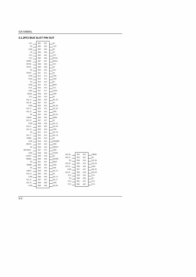
5.1.2PCI BUS SLOT PIN OUT
B23
B24
B31
B05
B07
B10
B13
B15
B19
B21
B25
B29
B02
B04
B08
B11
B14
B17
B20
B26
B27
B01
B03
B06
B09
B12
B16
B18
B22
B28
B30
A05
A07
A10
A13
A15
A19
A21
A02
A04
A08
A11
A14
A17
A20
A01
A03
A06
A09
A12
A16
A18
A22
A23
A24
A31
A25
A29
A26
A27
A28
A30
B33
B34
B41
B35
B39
B36
B37
B32
B38
B40
A32
A33
A34
A41
A35
A39
A36
A37
A38
A40
B43
B44
B45
B49
B46
B47
B42
B48
A42
A43
A44
A45
A49
A46
A47
A48
B53
B54
B61
B55
B59
B56
B57
B52
B58
B60
A52
A53
A54
A61
A55
A59
A56
A57
A58
A60
B62 A62
NC
+12V
NC
NC
VCC
INTA#
INTC#
VCC
NC
VCC
NC
GND
GND
NC
NC
NC
NC
NC
NC
RST#
VCC
GNT#
GND
AD_30
AD_28
AD_26
GND
AD_24
IDSEL
NC
AD_22
AD_20
GND
AD_18
AD_16
FRAME#
GND
TRDY#
GND
STOP#
SDONE
SBO#
GND
PAR
AD_15
AD_13
AD_11
GND
AD_09
CBE#0
NC
AD_06
AD_04
GND
AD_02
AD_00
VCC
NC
VCC
VCC
NC
SERR#
NC
CBE#1
AD_14
GND
AD_12
AD_10
GND
AD_08
AD_07
NC
AD_05
AD_03
GND
AD_01
VCC
NC
VCC
VCC
AD_25
NC
CBE#3
AD_23
GND
AD_21
AD_19
NC
AD_17
CEB#2
GND
IRDY#
NC
DEVSEL#
GND
LOCK#
PERR#
VCC
INTB#
INTD#
PST#1
NC
PST#2
GND
GND
NC
GND
CLK
GND
REQ#
VCC
AD_31
AD_29
GND
AD_27
-12V
NC
GND
NC
VCC
AT Technical Information
5-3
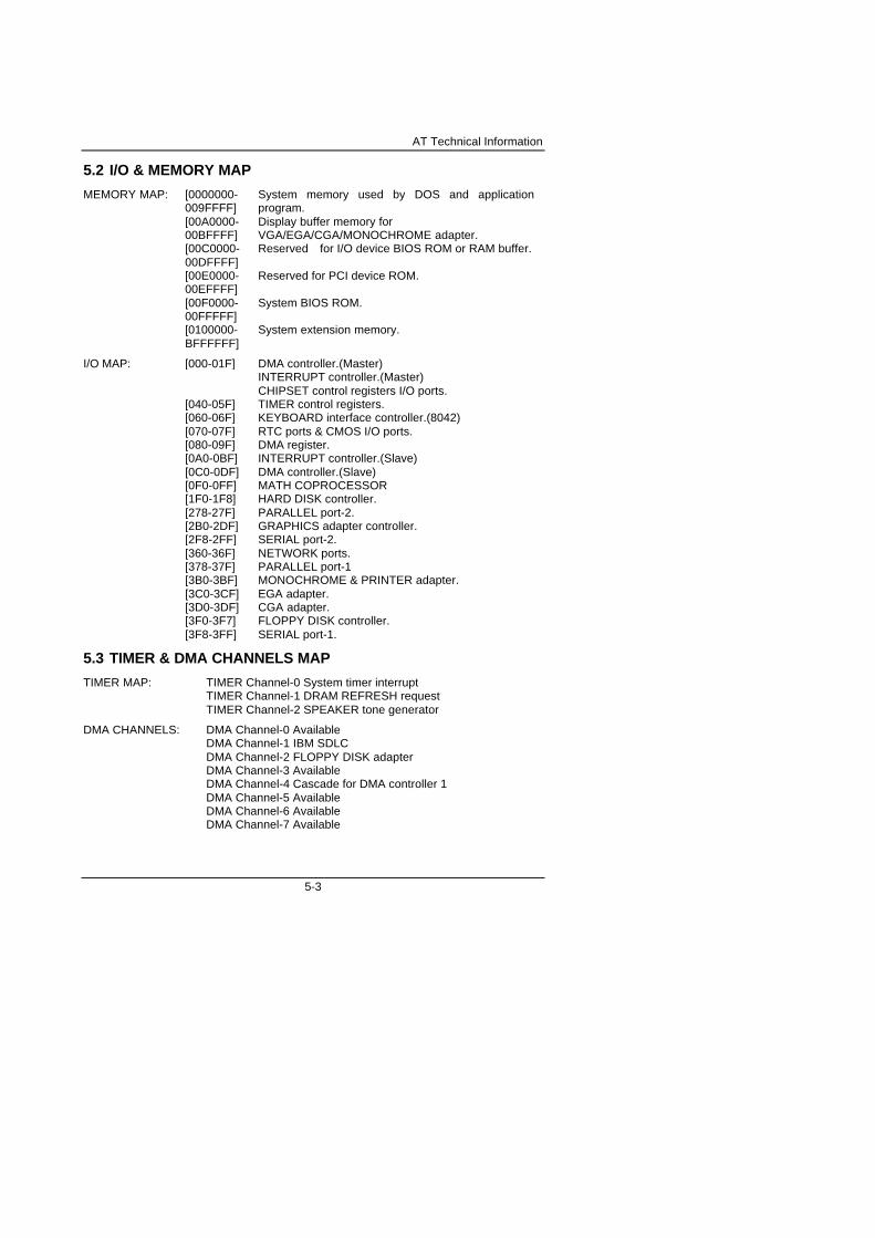
5.2 I/O & MEMORY MAP
MEMORY MAP: [0000000-009FFFF]
System memory used by DOS and applicationprogram.
[00A0000-00BFFFF]
Display buffer memory forVGA/EGA/CGA/MONOCHROME adapter.
[00C0000-00DFFFF]
Reserved for I/O device BIOS ROM or RAM buffer.
[00E0000-00EFFFF]
Reserved for PCI device ROM.
[00F0000-00FFFFF]
System BIOS ROM.
[0100000-BFFFFFF]
System extension memory.
I/O MAP: [000-01F] DMA controller.(Master)INTERRUPT controller.(Master)CHIPSET control registers I/O ports.
[040-05F] TIMER control registers.[060-06F] KEYBOARD interface controller.(8042)[070-07F] RTC ports & CMOS I/O ports.[080-09F] DMA register.[0A0-0BF] INTERRUPT controller.(Slave)[0C0-0DF] DMA controller.(Slave)[0F0-0FF] MATH COPROCESSOR[1F0-1F8] HARD DISK controller.[278-27F] PARALLEL port-2.[2B0-2DF] GRAPHICS adapter controller.[2F8-2FF] SERIAL port-2.[360-36F] NETWORK ports.[378-37F] PARALLEL port-1[3B0-3BF] MONOCHROME & PRINTER adapter.[3C0-3CF] EGA adapter.[3D0-3DF] CGA adapter.[3F0-3F7] FLOPPY DISK controller.[3F8-3FF] SERIAL port-1.
5.3 TIMER & DMA CHANNELS MAP
TIMER MAP: TIMER Channel-0 System timer interruptTIMER Channel-1 DRAM REFRESH requestTIMER Channel-2 SPEAKER tone generator
DMA CHANNELS: DMA Channel-0 AvailableDMA Channel-1 IBM SDLCDMA Channel-2 FLOPPY DISK adapterDMA Channel-3 AvailableDMA Channel-4 Cascade for DMA controller 1DMA Channel-5 AvailableDMA Channel-6 AvailableDMA Channel-7 Available
GA-5486AL
5-4
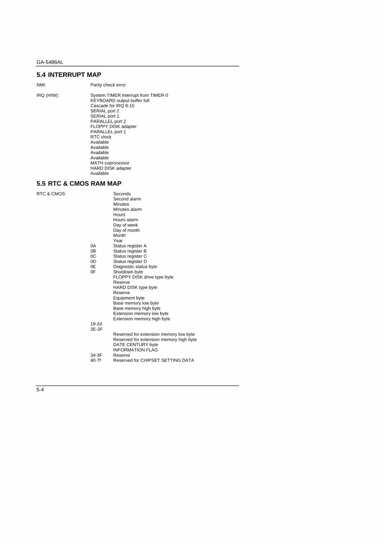
5.4 INTERRUPT MAPNMI: Parity check error
IRQ (H/W): System TIMER interrupt from TIMER-0KEYBOARD output buffer fullCascade for IRQ 8-15SERIAL port 2SERIAL port 1PARALLEL port 2FLOPPY DISK adapterPARALLEL port 1RTC clockAvailableAvailableAvailableAvailableMATH coprocessorHARD DISK adapterAvailable
5.5 RTC & CMOS RAM MAPRTC & CMOS: Seconds
Second alarmMinutesMinutes alarmHoursHours alarmDay of weekDay of monthMonthYear
0A Status register A0B Status register B0C Status register C0D Status register D0E Diagnostic status byte0F Shutdown byte
FLOPPY DISK drive type byteReserveHARD DISK type byteReserveEquipment byteBase memory low byteBase memory high byteExtension memory low byteExtension memory high byte
19-2d2E-2F
Reserved for extension memory low byteReserved for extension memory high byteDATE CENTURY byteINFORMATION FLAG
34-3F Reserve40-7f Reserved for CHIPSET SETTING DATA
Appendix A: Post Message
A-1
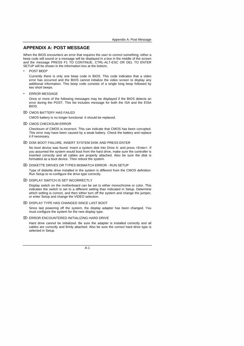
APPENDIX A: POST MESSAGEWhen the BIOS encounters an error that requires the user to correct something, either abeep code will sound or a message will be displayed in a box in the middle of the screenand the message PRESS F1 TO CONTINUE, CTRL-ALT-ESC OR DEL TO ENTERSETUP will be shown in the information box at the bottom.
• POST BEEP
Currently there is only one beep code in BIOS. This code indicates that a videoerror has occurred and the BIOS cannot initialize the video screen to display anyadditional information. This beep code consists of a single long beep followed bytwo short beeps.
• ERROR MESSAGE
Once or more of the following messages may be displayed if the BIOS detects anerror during the POST. This list includes message for both the ISA and the EISABIOS.
⌦ CMOS BATTERY HAS FAILED
CMOS battery is no longer functional. It should be replaced.
⌦ CMOS CHECKSUM ERROR
Checksum of CMOS is incorrect. This can indicate that CMOS has been corrupted.This error may have been caused by a weak battery. Check the battery and replaceit if necessary.
⌦ DISK BOOT FAILURE, INSERT SYSTEM DISK AND PRESS ENTER
No boot device was found. Insert a system disk into Drive A: and press <Enter>. Ifyou assumed the system would boot from the hard drive, make sure the controller isinserted correctly and all cables are properly attached. Also be sure the disk isformatted as a boot device. Then reboot the system.
⌦ DISKETTE DRIVES OR TYPES MISMATCH ERROR - RUN SETUP
Type of diskette drive installed in the system is different from the CMOS definition.Run Setup to re-configure the drive type correctly.
⌦ DISPLAY SWITCH IS SET INCORRECTLY
Display switch on the motherboard can be set to either monochrome or color. Thisindicates the switch is set to a different setting than indicated in Setup. Determinewhich setting is correct, and then either turn off the system and change the jumper,or enter Setup and change the VIDEO selection.
⌦ DISPLAY TYPE HAS CHANGED SINCE LAST BOOT
Since last powering off the system, the display adapter has been changed. Youmust configure the system for the new display type.
⌦ ERROR ENCOUNTERED INITIALIZING HARD DRIVE
Hard drive cannot be initialized. Be sure the adapter is installed correctly and allcables are correctly and firmly attached. Also be sure the correct hard drive type isselected in Setup.
GA-5486AL
A-2
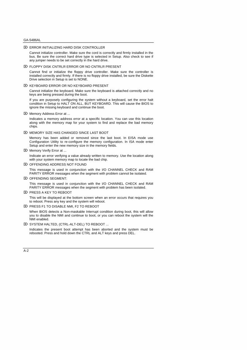
⌦ ERROR INITIALIZING HARD DISK CONTROLLER
Cannot initialize controller. Make sure the cord is correctly and firmly installed in thebus. Be sure the correct hard drive type is selected in Setup. Also check to see ifany jumper needs to be set correctly in the hard drive.
⌦ FLOPPY DISK CNTRLR ERROR OR NO CNTRLR PRESENT
Cannot find or initialize the floppy drive controller. Make sure the controller isinstalled correctly and firmly. If there is no floppy drive installed, be sure the DisketteDrive selection in Setup is set to NONE.
⌦ KEYBOARD ERROR OR NO KEYBOARD PRESENT
Cannot initialize the keyboard. Make sure the keyboard is attached correctly and nokeys are being pressed during the boot.
If you are purposely configuring the system without a keyboard, set the error haltcondition in Setup to HALT ON ALL, BUT KEYBOARD. This will cause the BIOS toignore the missing keyboard and continue the boot.
⌦ Memory Address Error at ...
Indicates a memory address error at a specific location. You can use this locationalong with the memory map for your system to find and replace the bad memorychips.
⌦ MEMORY SIZE HAS CHANGED SINCE LAST BOOT
Memory has been added or removed since the last boot. In EISA mode useConfiguration Utility to re-configure the memory configuration. In ISA mode enterSetup and enter the new memory size in the memory fields.
⌦ Memory Verify Error at ...
Indicate an error verifying a value already written to memory. Use the location alongwith your system memory map to locate the bad chip.
⌦ OFFENDING ADDRESS NOT FOUND
This message is used in conjunction with the I/O CHANNEL CHECK and RAMPARITY ERROR messages when the segment with problem cannot be isolated.
⌦ OFFENDING SEGMENT:
This message is used in conjunction with the I/O CHANNEL CHECK and RAMPARITY ERROR messages when the segment with problem has been isolated.
⌦ PRESS A KEY TO REBOOT
This will be displayed at the bottom screen when an error occurs that requires youto reboot. Press any key and the system will reboot.
⌦ PRESS F1 TO DISABLE NMI, F2 TO REBOOT
When BIOS detects a Non-maskable Interrupt condition during boot, this will allowyou to disable the NMI and continue to boot, or you can reboot the system will theNMI enabled.
⌦ SYSTEM HALTED, (CTRL-ALT-DEL) TO REBOOT ...
Indicates the present boot attempt has been aborted and the system must berebooted. Press and hold down the CTRL and ALT keys and press DEL.
Appendix B: Post Codes
B-1
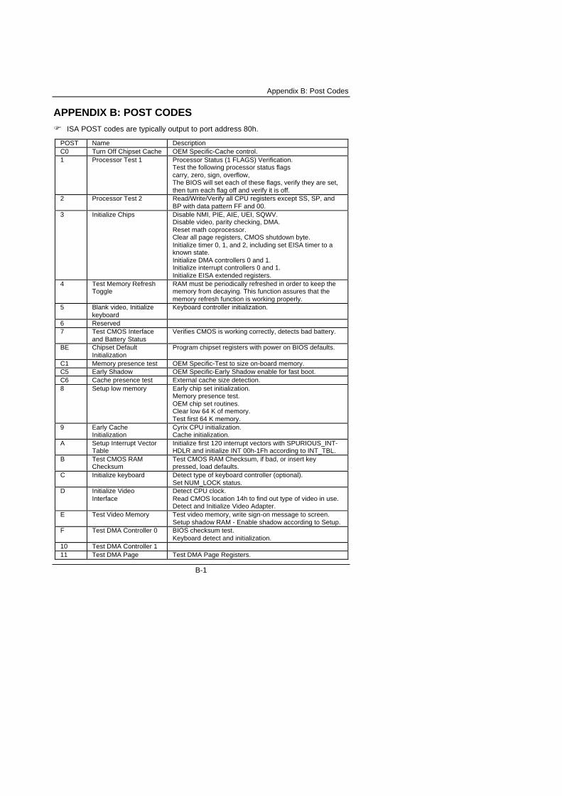
APPENDIX B: POST CODESF ISA POST codes are typically output to port address 80h.
POST Name DescriptionC0 Turn Off Chipset Cache OEM Specific-Cache control.1 Processor Test 1 Processor Status (1 FLAGS) Verification.
Test the following processor status flagscarry, zero, sign, overflow,The BIOS will set each of these flags, verify they are set,then turn each flag off and verify it is off.
2 Processor Test 2 Read/Write/Verify all CPU registers except SS, SP, andBP with data pattern FF and 00.
3 Initialize Chips Disable NMI, PIE, AIE, UEI, SQWV.Disable video, parity checking, DMA.Reset math coprocessor.Clear all page registers, CMOS shutdown byte.Initialize timer 0, 1, and 2, including set EISA timer to aknown state.Initialize DMA controllers 0 and 1.Initialize interrupt controllers 0 and 1.Initialize EISA extended registers.
4 Test Memory RefreshToggle
RAM must be periodically refreshed in order to keep thememory from decaying. This function assures that thememory refresh function is working properly.
5 Blank video, Initializekeyboard
Keyboard controller initialization.
6 Reserved7 Test CMOS Interface
and Battery StatusVerifies CMOS is working correctly, detects bad battery.
BE Chipset DefaultInitialization
Program chipset registers with power on BIOS defaults.
C1 Memory presence test OEM Specific-Test to size on-board memory.C5 Early Shadow OEM Specific-Early Shadow enable for fast boot.C6 Cache presence test External cache size detection.8 Setup low memory Early chip set initialization.
Memory presence test.OEM chip set routines.Clear low 64 K of memory.Test first 64 K memory.
9 Early CacheInitialization
Cyrix CPU initialization.Cache initialization.
A Setup Interrupt VectorTable
Initialize first 120 interrupt vectors with SPURIOUS_INT-HDLR and initialize INT 00h-1Fh according to INT_TBL.
B Test CMOS RAMChecksum
Test CMOS RAM Checksum, if bad, or insert keypressed, load defaults.
C Initialize keyboard Detect type of keyboard controller (optional).Set NUM_LOCK status.
D Initialize VideoInterface
Detect CPU clock.Read CMOS location 14h to find out type of video in use.Detect and Initialize Video Adapter.
E Test Video Memory Test video memory, write sign-on message to screen.Setup shadow RAM - Enable shadow according to Setup.
F Test DMA Controller 0 BIOS checksum test.Keyboard detect and initialization.
10 Test DMA Controller 111 Test DMA Page Test DMA Page Registers.
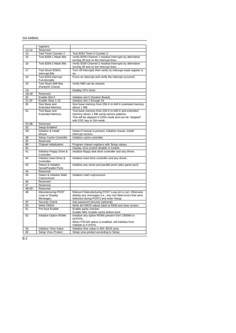
GA-5486AL
B-2
registers12-13 Reserved14 Test Timer Counter 2 Test 8254 Timer 0 Counter 2.15 Test 8259-1 Mask Bits Verify 8259 Channel 1 masked interrupts by alternative
turning off and on the interrupt lines.16 Test 8259-2 Mask Bits Verify 8259 Channel 2 masked interrupts by alternative
turning off and on the interrupt lines.17 Test Stuck 8259's
Interrupt BitsTurn off interrupts then verify no interrupt mask register ison.
18 Test 8259 InterruptFunctionality
Force an interrupt and verify the interrupt occurred.
19 Test Stuck NMI Bits(Parity/IO Check)
Verify NMI can be cleared.
1A Display CPU clock.1B-1E Reserved20 Enable Slot 0 Initialize slot 0 (System Board).21-2F Enable Slots 1-15 Initialize slot 1 through 15.30 Size Base and
Extended MemorySize base memory from 256 K to 640 K extended memoryabove 1 MB.
31 Test Base andExtended Memory
Test base memory from 256 K to 640 K and extendedmemory above 1 MB using various patterns.This will be skipped in EISA mode and can be "skipped"with ESC key in ISA mode.
33-3B Reserved3C Setup Enabled3D Initialize & Install
MouseDetect if mouse is present, initialize mouse, installinterrupt vectors.
3E Setup Cache Controller Initialize cache controller.3F ReservedBF Chipset Initialization Program chipset registers with Setup values.40 Display virus protest disable or enable.41 Initialize Floppy Drive &
ControllerInitialize floppy disk drive controller and any drives.
42 Initialize Hard Drive &Controller
Initialize hard drive controller and any drives.
43 Detect & InitializeSerial/Parallel Ports
Initialize any serial and parallel ports (also game port).
44 Reserved45 Detect & Initialize Math
CoprocessorInitialize math coprocessor.
46 Reserved47 Reserved48-4D Reserved4E Manufacturing POST
Loop or DisplayMessages
Reboot if Manufacturing POST Loop pin is set. Otherwisedisplay any messages (i.e., any non-fatal errors that weredetected during POST) and enter Setup.
4F Security Check Ask password security (optional).50 Write CMOS Write all CMOS values back to RAM and clear screen.51 Pre-boot Enable Enable parity checker.
Enable NMI, Enable cache before boot.52 Initialize Option ROMs Initialize any option ROMs present from C8000h to
EFFFFh.When FSCAN option is enabled, will initialize fromC8000h to F7FFFh.
53 Initialize Time Value Initialize time value in 40h: BIOS area.60 Setup Virus Protect Setup virus protect according to Setup

Appendix B: Post Codes
B-3
61 Set Boot Speed Set system speed for boot62 Setup NumLock Setup NumLock status according to Setup63 Boot Attempt Set low stack.
Boot via INT 19h.B0 Spurious If interrupt occurs in protected mode.B1 Unclaimed NMI If unmasked NMI occurs, display
Press F1 to disable NMI, F2 reboot.E1-EF Setup Pages E1 - Page 1, E2 - Page 2, etc.FF Boot

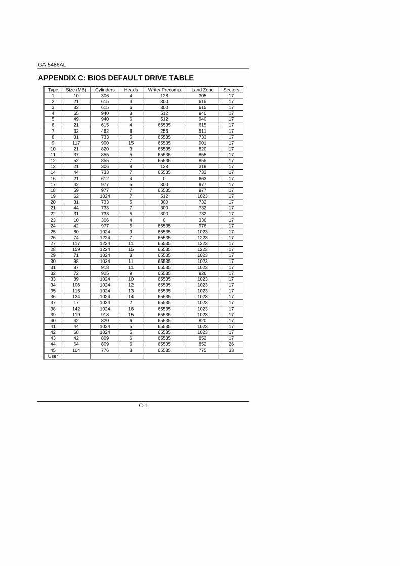
GA-5486AL
C-1
APPENDIX C: BIOS DEFAULT DRIVE TABLEType Size (MB) Cylinders Heads Write/ Precomp Land Zone Sectors
1 10 306 4 128 305 172 21 615 4 300 615 173 32 615 6 300 615 174 65 940 8 512 940 175 49 940 6 512 940 176 21 615 4 65535 615 177 32 462 8 256 511 178 31 733 5 65535 733 179 117 900 15 65535 901 1710 21 820 3 65535 820 1711 37 855 5 65535 855 1712 52 855 7 65535 855 1713 21 306 8 128 319 1714 44 733 7 65535 733 1716 21 612 4 0 663 1717 42 977 5 300 977 1718 59 977 7 65535 977 1719 62 1024 7 512 1023 1720 31 733 5 300 732 1721 44 733 7 300 732 1722 31 733 5 300 732 1723 10 306 4 0 336 1724 42 977 5 65535 976 1725 80 1024 9 65535 1023 1726 74 1224 7 65535 1223 1727 117 1224 11 65535 1223 1728 159 1224 15 65535 1223 1729 71 1024 8 65535 1023 1730 98 1024 11 65535 1023 1731 87 918 11 65535 1023 1732 72 925 9 65535 926 1733 89 1024 10 65535 1023 1734 106 1024 12 65535 1023 1735 115 1024 13 65535 1023 1736 124 1024 14 65535 1023 1737 17 1024 2 65535 1023 1738 142 1024 16 65535 1023 1739 119 918 15 65535 1023 1740 42 820 6 65535 820 1741 44 1024 5 65535 1023 1742 68 1024 5 65535 1023 1743 42 809 6 65535 852 1744 64 809 6 65535 852 2645 104 776 8 65535 775 33
User

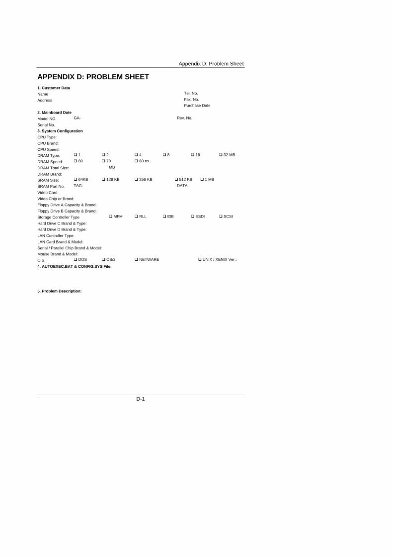
Appendix D: Problem Sheet
D-1
APPENDIX D: PROBLEM SHEET1. Customer Data
Name Tel. No.
Address Fax. No.
Purchase Date
2. Mainboard Date
Model NO. GA- Rev. No.
Serial No.
3. System Configuration
CPU Type:
CPU Brand:
CPU Speed:
DRAM Type: q 1 q 2 q 4 q 8 q 16 q 32 MB
DRAM Speed: q 80 q 70 q 60 ns
DRAM Total Size: MB
DRAM Brand:
SRAM Size: q 64KB q 128 KB q 256 KB q 512 KB q 1 MB
SRAM Part No. TAG: DATA:
Video Card:
Video Chip or Brand:
Floppy Drive A Capacity & Brand:
Floppy Drive B Capacity & Brand:
Storage Controller Type q MFM q RLL q IDE q ESDI q SCSI
Hard Drive C Brand & Type:
Hard Drive D Brand & Type:
LAN Controller Type:
LAN Card Brand & Model:
Serial / Parallel Chip Brand & Model:
Mouse Brand & Model:
O.S. q DOS q OS/2 q NETWARE q UNIX / XENIX Ver.:
4. AUTOEXEC.BAT & CONFIG.SYS File:
5. Problem Description: