Embed Size (px)
Citation preview
FYS4260/FYS9260: Microsystems and
Electronics Packaging and Interconnect
Metallization and
Interconnects
Learning objectives
• Metal heros
• Significance of selecting right metallization systems and examples of failure modes
• Flip-chip bonding
• Stud bumping
• Die attach
• Conductive adhesives
• Background literature: – Halbo & Ohlckers Chapter 6 and 7
– The HDI handbook
– Malestroem: The printed circuit handbook 6th ed.
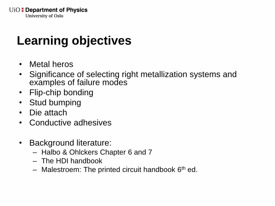
The electronics metallisation super-heros
We want low resistivity!
The best conductors in nature are
1. Silver (1.60 µΩ−cm)
2. Copper (1.67 µΩ−cm)
3. Gold (2.3 µΩ−cm)
4. Aluminum (2.69 µΩ−cm)
… Tin (11.0 µΩ−cm)
Silver is widely used in electronics, but still does not
make the heros list because…
FYS4260/FYS9260 Frode Strisland 3
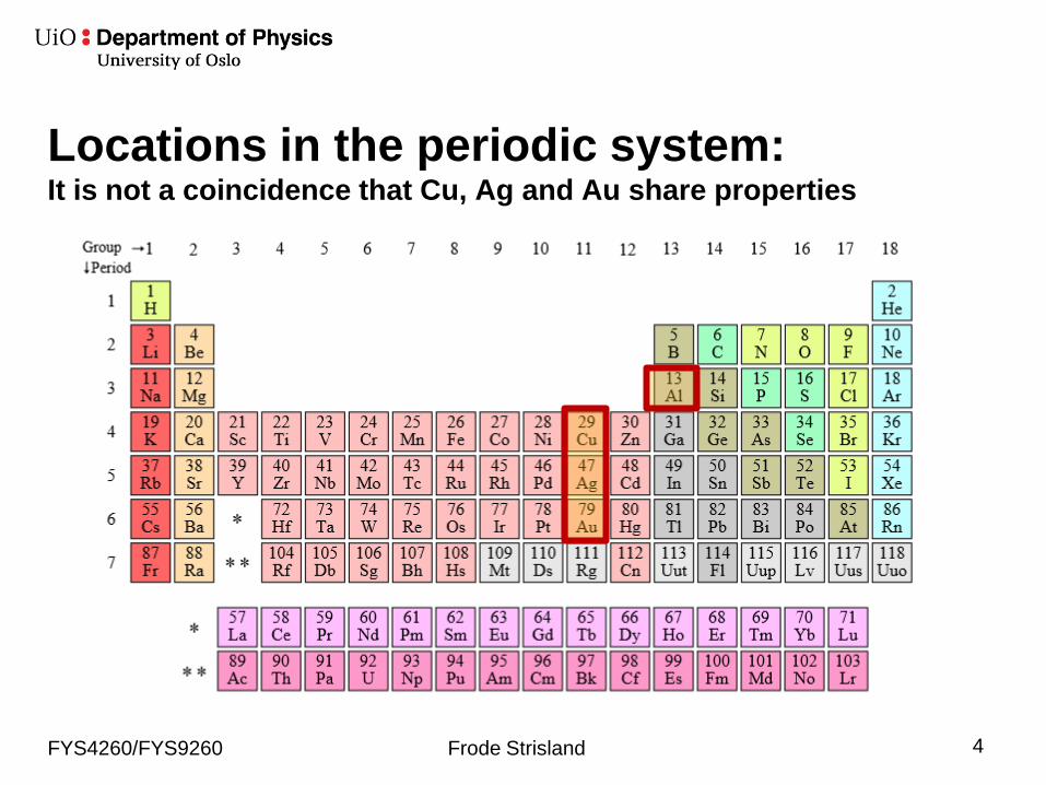
Locations in the periodic system: It is not a coincidence that Cu, Ag and Au share properties
FYS4260/FYS9260 Frode Strisland 4
Silver in metallisation
Excellent electrical conductivity (the best you can buy). Frequently used in glass and adhesive mixtures as conductive ingredient.
Ag is a VERY fast diffuser in dielectrics, especially when driven by an electric field. The rapid diffusion is because diffusion happens as an Ag+ ion which is much smaller in size than the neutral Ag atom, and thus moves easily. Susceptible for electromigration.
Pure Ag also quickly forms oxides. Ag is also relatively expensive in value-for-money terms.
FYS4260/FYS9260 Frode Strisland 5
The metallization heros:
Aluminium (Al)
The final metal layer of most IC bond pads is
sputter deposited aluminum, providing a
satisfactory surface for conventional wire bonding.
Al can be shaped into fine wires applied for wedge-
wedge Al bonding. Al immediately forms oxides in
air. Aluminum is not a readily solderable surface,
neither wettable nor bondable by most solders.
Aluminum may corrode over time when not
protected from the environment.
Low melting temperature (660°C), limiting its use in
ceramic hybrids. FYS4260/FYS9260 Frode Strisland 6
The metallization heros:
Gold (Au)
Gold is the metallization superhero; highly
conductive and ductile. It does not corrode and is
frequently used as a protective layer. Diffuses
easily, for example into tin, as well as into
unprotected silicon in which it can destroy
semiconducting band-gaps. Gold is therefore
strictly forbidden in several IC and microsystems
processing facilities.
FYS4260/FYS9260 Frode Strisland 7
The metallization heros:
Tin (Sn)
Tin is a soft, ductile, low melting point metal that wets
and blends in whereever it can! The electrical
conductivity of Sn is not comparable to Al,Au, and
Cu, but the material is still valuable in solder
applications in particular. Sn is responsible for the
reduced soldering temperature in most (bi-/multi-
metal) soldering compositions. Tin has a reasonable
resistance towards the environment, making it an
acceptable surface finish for printed circuit boards.
Can create whiskers that causes reliability concerns.
FYS4260/FYS9260 Frode Strisland 8
The metallization heros:
Copper (Cu)
Copper is the PCB metallization workhorse.
Conductivity comparable to silver. Cu can be
electro- and electroless plated on many surfaces.
Excellent electrical and thermal conductivity and
ductile. Oxidises in air so flux treatment is needed
prior to soldering. Cu is also increasingly applied as
IC metallization.
FYS4260/FYS9260 Frode Strisland 9
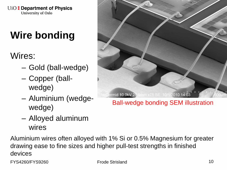
Wire bonding
Wires:
– Gold (ball-wedge)
– Copper (ball-
wedge)
– Aluminium (wedge-
wedge)
– Alloyed aluminum
wires
FYS4260/FYS9260 Frode Strisland 10
Ball-wedge bonding SEM illustration
Aluminium wires often alloyed with 1% Si or 0.5% Magnesium for greater
drawing ease to fine sizes and higher pull-test strengths in finished
devices
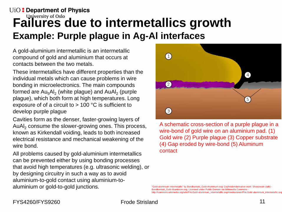
Failures due to intermetallics growth Example: Purple plague in Ag-Al interfaces
A gold-aluminium intermetallic is an intermetallic
compound of gold and aluminium that occurs at
contacts between the two metals.
These intermetallics have different properties than the
individual metals which can cause problems in wire
bonding in microelectronics. The main compounds
formed are Au5Al2 (white plague) and AuAl2 (purple
plague), which both form at high temperatures. Long
exposure of of a circuit to > 100 °C is sufficient to
develop purple plague
Cavities form as the denser, faster-growing layers of
AuAl2 consume the slower-growing ones. This process,
known as Kirkendall voiding, leads to both increased
electrical resistance and mechanical weakening of the
wire bond.
All problems caused by gold-aluminium intermetallics
can be prevented either by using bonding processes
that avoid high temperatures (e.g. ultrasonic welding), or
by designing circuitry in such a way as to avoid
aluminium-to-gold contact using aluminium-to-
aluminium or gold-to-gold junctions.
FYS4260/FYS9260 Frode Strisland 11
"Gold-aluminium intermetallic" by Bondkontakt_Gold-Aluminium.svg: Cepheidenderivative work: Shoecream (talk) -
Bondkontakt_Gold-Aluminium.svg. Licensed under Public Domain via Wikimedia Commons -
http://commons.wikimedia.org/wiki/File:Gold-aluminium_intermetallic.svg#mediaviewer/File:Gold-aluminium_intermetallic.svg
A schematic cross-section of a purple plague in a
wire-bond of gold wire on an aluminium pad. (1)
Gold wire (2) Purple plague (3) Copper substrate
(4) Gap eroded by wire-bond (5) Aluminum
contact
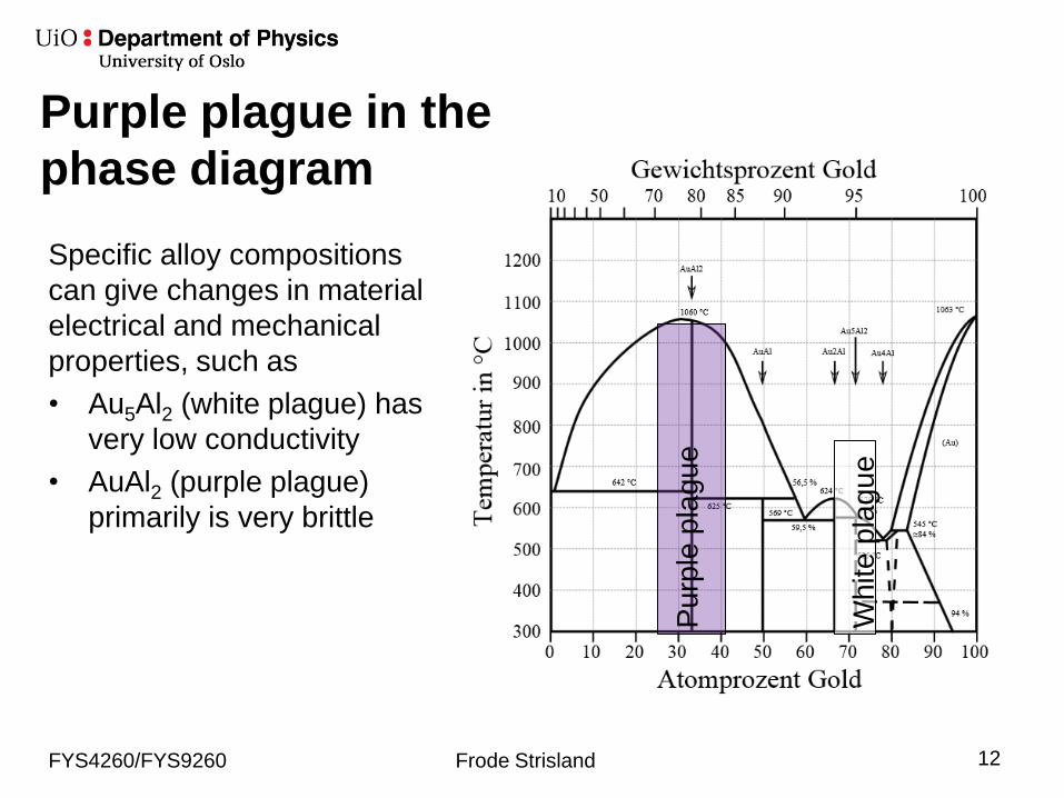
Purple plague in the
phase diagram
Specific alloy compositions
can give changes in material
electrical and mechanical
properties, such as
• Au5Al2 (white plague) has
very low conductivity
• AuAl2 (purple plague)
primarily is very brittle
FYS4260/FYS9260 Frode Strisland 12
Pu
rple
pla
gu
e
Wh
ite
pla
gu
e
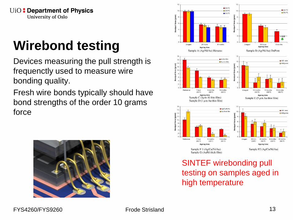
Wirebond testing Devices measuring the pull strength is
frequenctly used to measure wire
bonding quality.
Fresh wire bonds typically should have
bond strengths of the order 10 grams
force
FYS4260/FYS9260 Frode Strisland 13
SINTEF wirebonding pull
testing on samples aged in
high temperature
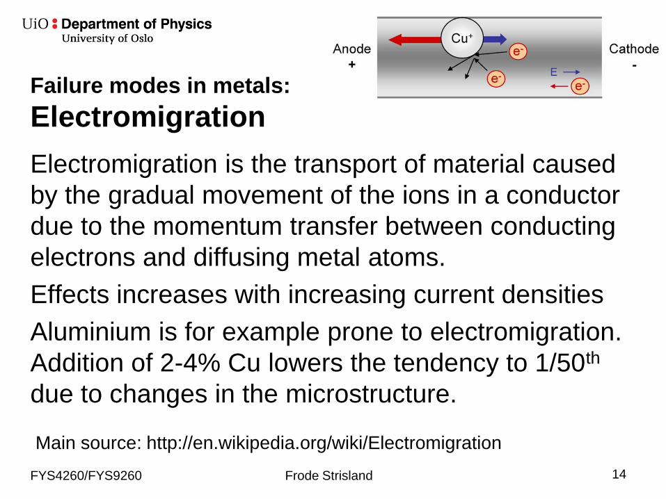
Failure modes in metals:
Electromigration
Electromigration is the transport of material caused
by the gradual movement of the ions in a conductor
due to the momentum transfer between conducting
electrons and diffusing metal atoms.
Effects increases with increasing current densities
Aluminium is for example prone to electromigration.
Addition of 2-4% Cu lowers the tendency to 1/50th
due to changes in the microstructure.
FYS4260/FYS9260 Frode Strisland 14
Main source: http://en.wikipedia.org/wiki/Electromigration
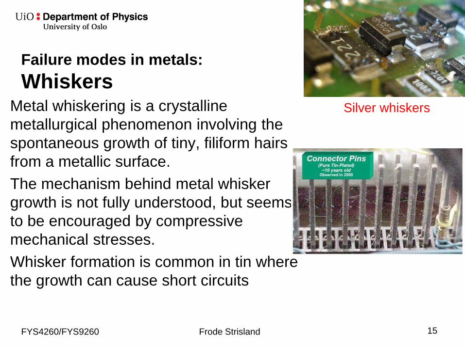
Failure modes in metals:
Whiskers Metal whiskering is a crystalline
metallurgical phenomenon involving the
spontaneous growth of tiny, filiform hairs
from a metallic surface.
The mechanism behind metal whisker
growth is not fully understood, but seems
to be encouraged by compressive
mechanical stresses.
Whisker formation is common in tin where
the growth can cause short circuits
FYS4260/FYS9260 Frode Strisland 15
Silver whiskers
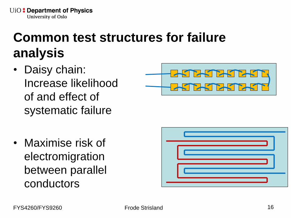
Common test structures for failure
analysis
• Daisy chain:
Increase likelihood
of and effect of
systematic failure
• Maximise risk of
electromigration
between parallel
conductors
FYS4260/FYS9260 Frode Strisland 16
Pad metallization
Depending on the application and materials used, a
number of functions must be impelemented on a
electrical pad. This is usually implemented in a
layer-by-layer approach.
FYS4260/FYS9260 Frode Strisland 17
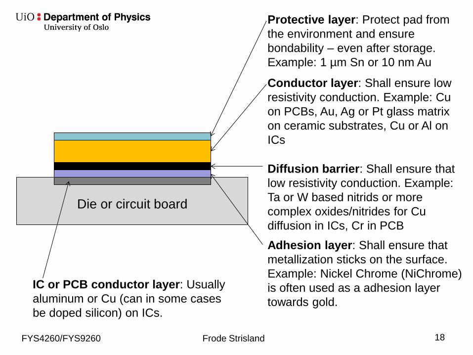
Die or circuit board
• Protective layer
• Conductor layer
• Diffusion barrier
• Adhesive layer
• Conductor integrated
FYS4260/FYS9260 Frode Strisland 18
Die or circuit board
Protective layer: Protect pad from
the environment and ensure
bondability – even after storage.
Example: 1 µm Sn or 10 nm Au
Conductor layer: Shall ensure low
resistivity conduction. Example: Cu
on PCBs, Au, Ag or Pt glass matrix
on ceramic substrates, Cu or Al on
ICs
Diffusion barrier: Shall ensure that
low resistivity conduction. Example:
Ta or W based nitrids or more
complex oxides/nitrides for Cu
diffusion in ICs, Cr in PCB
Adhesion layer: Shall ensure that
metallization sticks on the surface.
Example: Nickel Chrome (NiChrome)
is often used as a adhesion layer
towards gold.
IC or PCB conductor layer: Usually
aluminum or Cu (can in some cases
be doped silicon) on ICs.
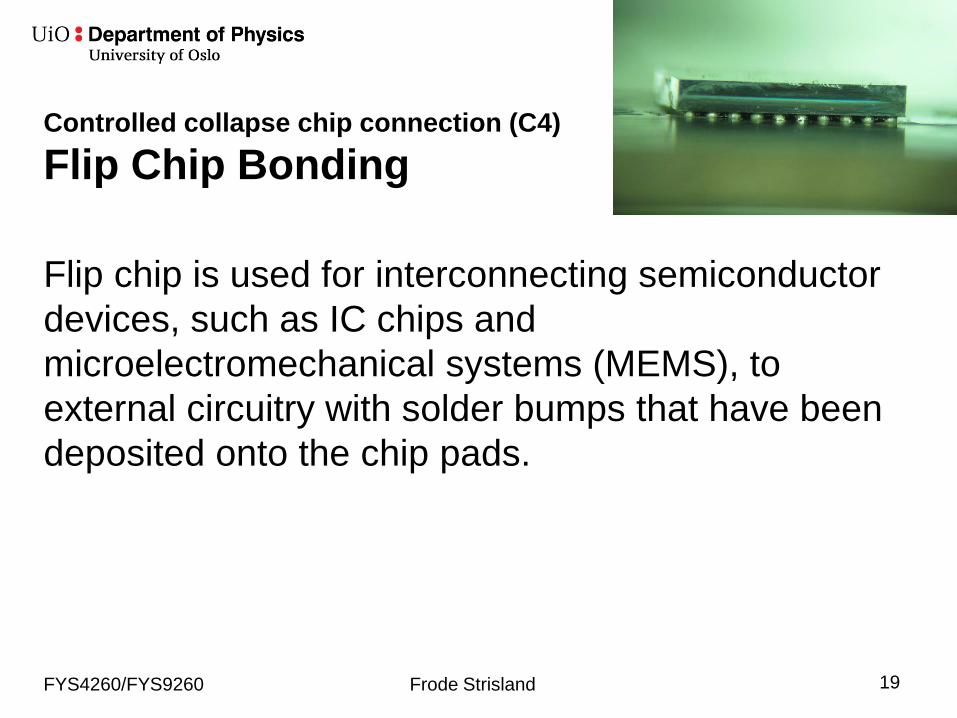
Controlled collapse chip connection (C4)
Flip Chip Bonding
Flip chip is used for interconnecting semiconductor
devices, such as IC chips and
microelectromechanical systems (MEMS), to
external circuitry with solder bumps that have been
deposited onto the chip pads.
FYS4260/FYS9260 Frode Strisland 19

Under-Bump Metallization in FlipChip
bonding1)
It is not possible to solder directly to Al (oxide) pads. An under-bump metallization (UBM) is therefore needed:
• It must provide a strong, stable, low resistance electrical connection to the aluminum.
• It must adhere well both to the underlying aluminum and to the surrounding IC passivation layer, hermetically sealing the aluminum from the environment.
• The UBM must provide a strong barrier to prevent the diffusion of other bump metals into the IC.
• The UBM must be readily wettable by the bump metals, for solder reflow
FYS4260/FYS9260 Frode Strisland 20
1) This and subsequent UBM slide are based on material from
http://flipchips.com/tutorial/process/under-bump-metallization-ubm/
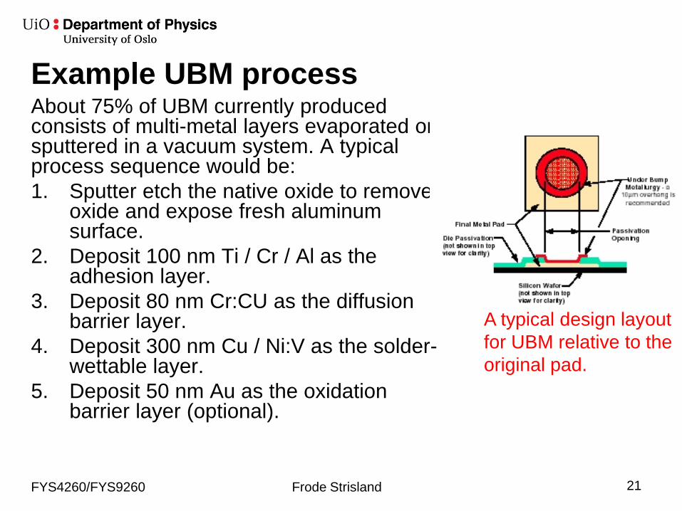
Example UBM process About 75% of UBM currently produced consists of multi-metal layers evaporated or sputtered in a vacuum system. A typical process sequence would be:
1. Sputter etch the native oxide to remove oxide and expose fresh aluminum surface.
2. Deposit 100 nm Ti / Cr / Al as the adhesion layer.
3. Deposit 80 nm Cr:CU as the diffusion barrier layer.
4. Deposit 300 nm Cu / Ni:V as the solder-wettable layer.
5. Deposit 50 nm Au as the oxidation barrier layer (optional).
FYS4260/FYS9260 Frode Strisland 21
A typical design layout
for UBM relative to the
original pad.
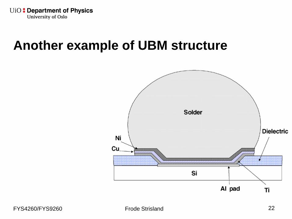
Another example of UBM structure
FYS4260/FYS9260 Frode Strisland 22
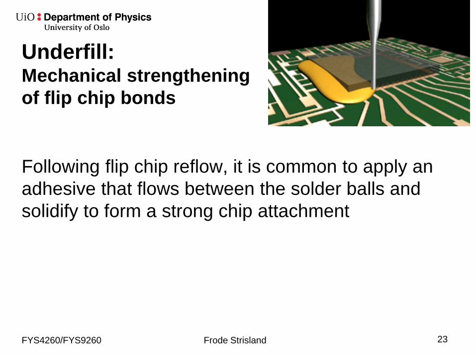
Underfill: Mechanical strengthening
of flip chip bonds
Following flip chip reflow, it is common to apply an
adhesive that flows between the solder balls and
solidify to form a strong chip attachment
FYS4260/FYS9260 Frode Strisland 23
Administrativ info
• Neste forelesning: Tykk- og tynnfilmhybrider
• Husk hard frist for utlegg: 23. mars kl 2395 til
• Øvinger: Sender ut løsningsforslag en av de
nærmeste dagene.
FYS4260/FYS9260 Frode Strisland 24
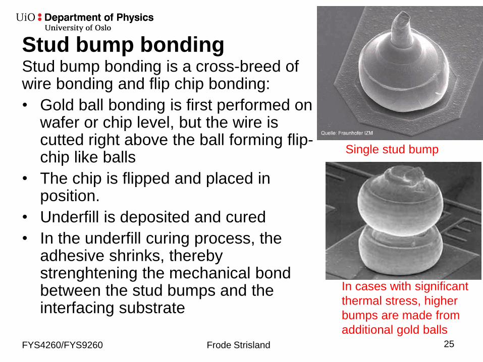
Stud bump bonding Stud bump bonding is a cross-breed of wire bonding and flip chip bonding:
• Gold ball bonding is first performed on wafer or chip level, but the wire is cutted right above the ball forming flip-chip like balls
• The chip is flipped and placed in position.
• Underfill is deposited and cured
• In the underfill curing process, the adhesive shrinks, thereby strenghtening the mechanical bond between the stud bumps and the interfacing substrate
FYS4260/FYS9260 Frode Strisland 25
Single stud bump
In cases with significant
thermal stress, higher
bumps are made from
additional gold balls
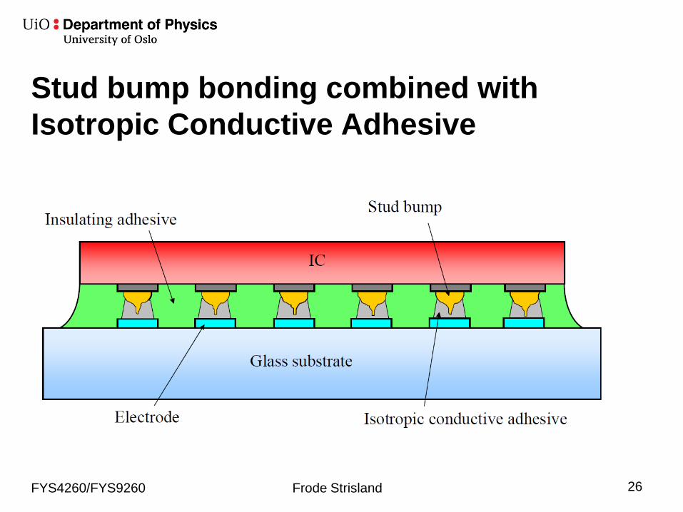
Stud bump bonding combined with
Isotropic Conductive Adhesive
FYS4260/FYS9260 Frode Strisland 26
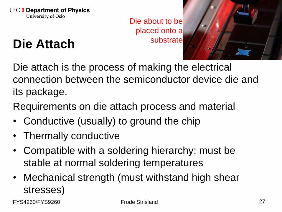
Die Attach
Die attach is the process of making the electrical
connection between the semiconductor device die and
its package.
Requirements on die attach process and material
• Conductive (usually) to ground the chip
• Thermally conductive
• Compatible with a soldering hierarchy; must be
stable at normal soldering temperatures
• Mechanical strength (must withstand high shear
stresses)
FYS4260/FYS9260 Frode Strisland 27
Die about to be
placed onto a
substrate
Die Attach
Common approaches
• High temperature soldering (hard solders, good
thermal conductivity)
– AuSi (420°C) and AuSn (350°C)
– High lead, e.g. Pb90Sn10 (300°C)
• Adhesives (high tensile stresses from curing,
moderate thermal conductivity)
– Silver filled adhesives: Epoxy resin that has been
highly loaded with silver metal flakes
FYS4260/FYS9260 Frode Strisland 28
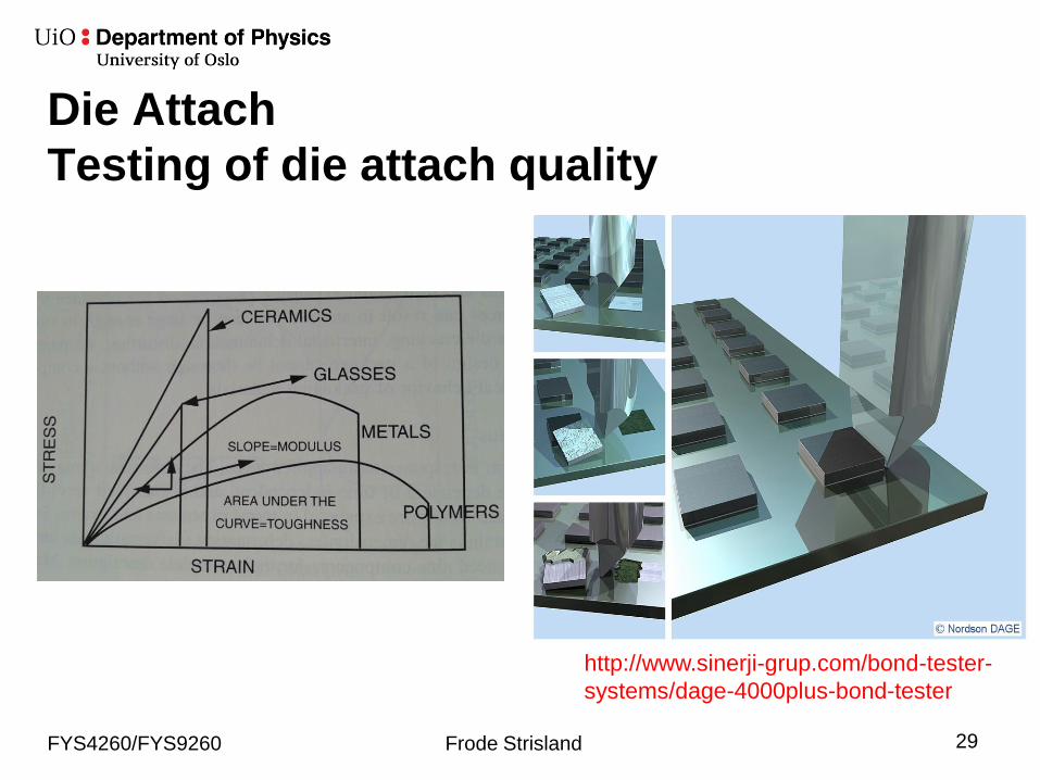
Die Attach
Testing of die attach quality
FYS4260/FYS9260 Frode Strisland 29
http://www.sinerji-grup.com/bond-tester-
systems/dage-4000plus-bond-tester
Adhesives in Electronics
• Adhesives categorized into
– Non-conductive adhesives
– Isotropic Conductive Adhesives
– Anisotropic Conductive Adhesives
FYS4260/FYS9260 Frode Strisland 30
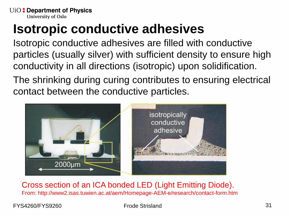
Isotropic conductive adhesives Isotropic conductive adhesives are filled with conductive
particles (usually silver) with sufficient density to ensure high
conductivity in all directions (isotropic) upon solidification.
The shrinking during curing contributes to ensuring electrical
contact between the conductive particles.
FYS4260/FYS9260 Frode Strisland 31
Cross section of an ICA bonded LED (Light Emitting Diode). From: http://www2.isas.tuwien.ac.at/aem/Homepage-AEM-e/research/contact-form.htm
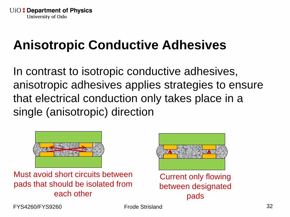
Anisotropic Conductive Adhesives
In contrast to isotropic conductive adhesives,
anisotropic adhesives applies strategies to ensure
that electrical conduction only takes place in a
single (anisotropic) direction
FYS4260/FYS9260 Frode Strisland 32
Must avoid short circuits between
pads that should be isolated from
each other
Current only flowing
between designated
pads
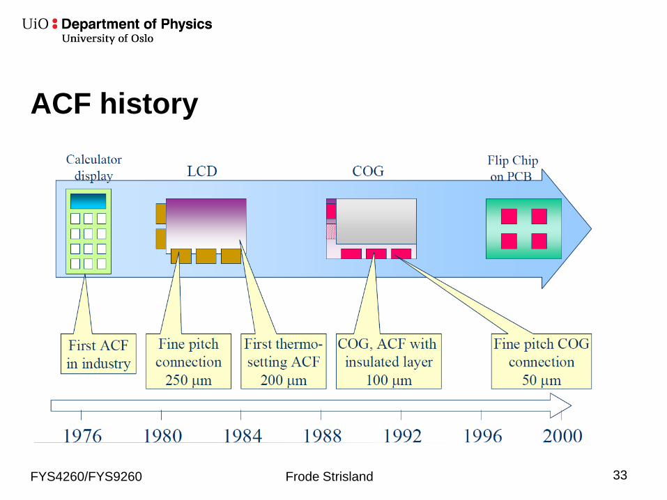
ACF history
FYS4260/FYS9260 Frode Strisland 33
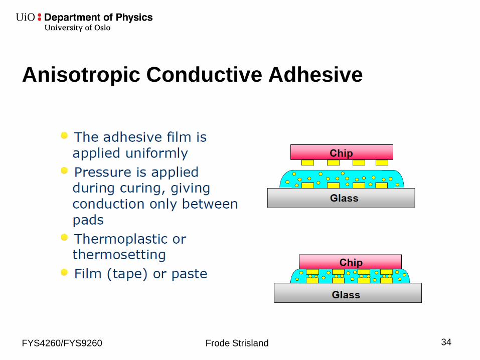
Anisotropic Conductive Adhesive
FYS4260/FYS9260 Frode Strisland 34
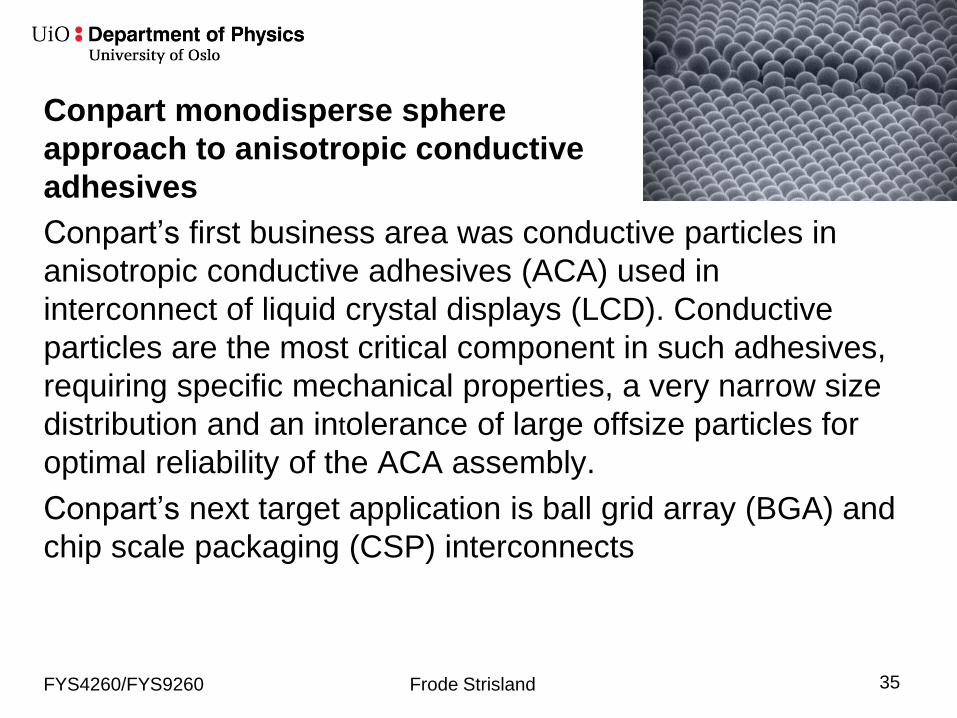
Conpart monodisperse sphere
approach to anisotropic conductive
adhesives
Conpart’s first business area was conductive particles in
anisotropic conductive adhesives (ACA) used in
interconnect of liquid crystal displays (LCD). Conductive
particles are the most critical component in such adhesives,
requiring specific mechanical properties, a very narrow size
distribution and an intolerance of large offsize particles for
optimal reliability of the ACA assembly.
Conpart’s next target application is ball grid array (BGA) and
chip scale packaging (CSP) interconnects
FYS4260/FYS9260 Frode Strisland 35
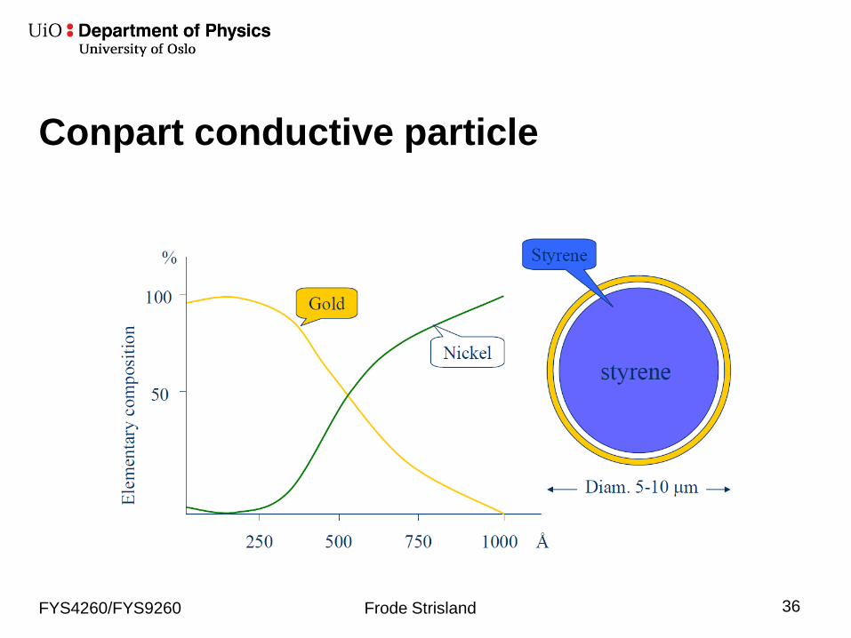
Conpart conductive particle
FYS4260/FYS9260 Frode Strisland 36
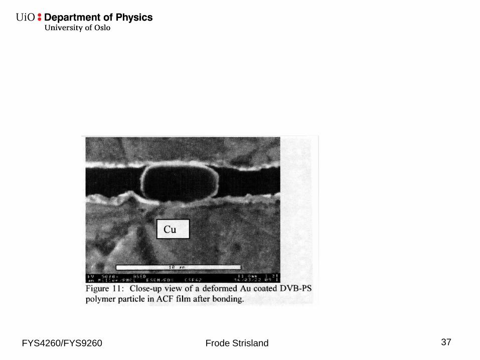
FYS4260/FYS9260 Frode Strisland 37
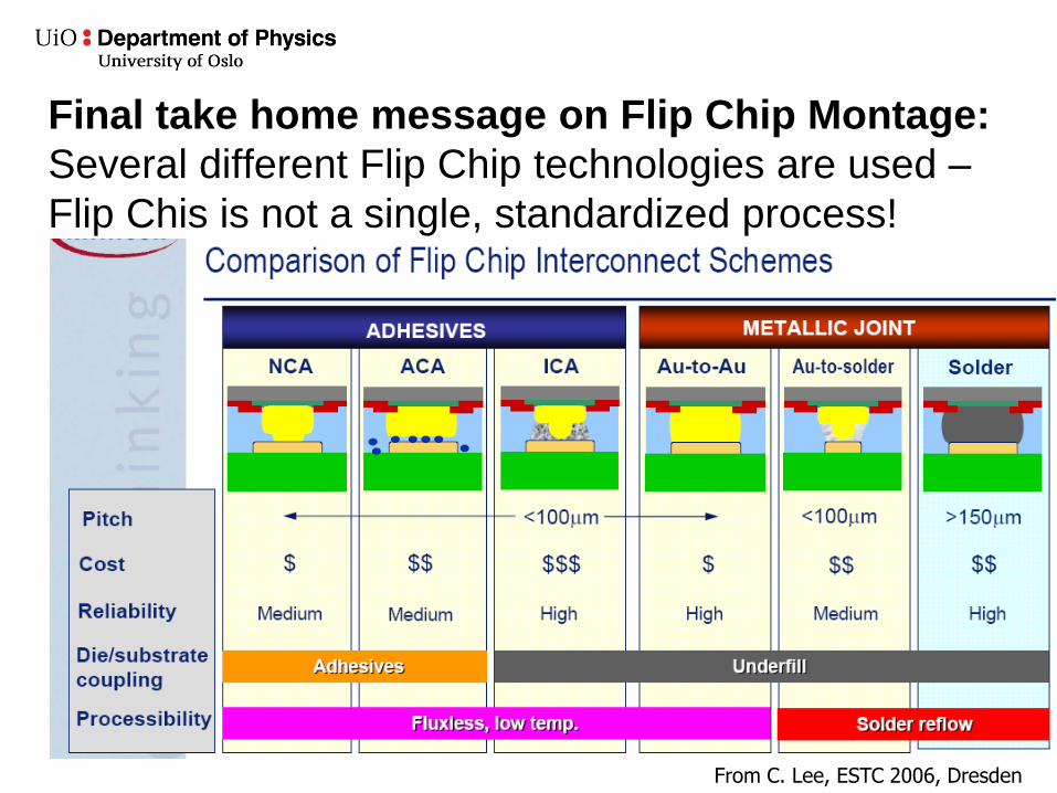
Final take home message on Flip Chip Montage:
Several different Flip Chip technologies are used –
Flip Chis is not a single, standardized process!
From C. Lee, ESTC 2006, Dresden
End of lecture:
Metallization and Interconnections
• Important issues:
– Metals are different, and a lot of things takes place
on the atomic scale
– You should be able to explain the various ways to
electrically connect a die to a circuit board or
package