Embed Size (px)
Citation preview

Fuzzy Control Design for Quasi-Z-Source
Three Phase Inverter
نوع من طوارأ ةلدائرة تحويل ذات ثالثكم ضبابي تحم تصميم
Quasi-Z-Source
Nouh A. Qaoud
Supervised by
Dr.Basil Hamed
Associate prof. of Control Systems
A thesis submitted in partial fulfilment
of the requirements for the degree of
Master of Electrical Engineering
June/2016
غــزة – اإلســـــالميــة الجـامعــــــــــة
االبحث العلمي والدراسات العلي شئون
ةـــــــــــــدســـنـــهــال ةــــــيـــــــلــــك
ائيةـربـهـكـال ةـدسـنـاله رـيـتـسـاجــم
مـــكـــــحــــتأنـــظــمة ةــــدســنــــه
The Islamic University–Gaza
Research and Postgraduate Affairs
Faculty of Engineering
Master of Electrical Engineering
Control Systems Engineering

إقــــــــــــــرار
أنا الموقع أدناه مقدم الرسالة التي تحمل العنوان:
Fuzzy Control Design for Quasi-Z-Source Three Phase
Inverter
من نوعتصميم متحكم ضبابي لدائرة تحويل ذات ثالثة أطوار
Quasi-Z-Source
أقر بأن ما اشتملت عليه هذه الرسالة إنما هو نتاج جهدي الخاص، باستثناء ما تمت اإلشارة إليه حيثما ورد، وأن هذه
لنيل درجة أو لقب علمي أو بحثي لدى أي مؤسسة تعليمية أو االخرين الرسالة ككل أو أي جزء منها لم يقدم من قبل
بحثية أخرى.
Declaration
I understand the nature of plagiarism, and I am aware of the University’s policy on
this.
The work provided in this thesis, unless otherwise referenced, is the researcher's own work,
and has not been submitted by others elsewhere for any other degree or qualification.
:Student's name نوح علي قاعود اسم الطالب:
:Signature التوقيع:
:Date 15/6/2016 التاريخ:


I
DEDICATION
I dedicate this thesis to my father, my wife and my little kid Ali in recognition of their
endless help and support; I also dedicate this work to my lovely brothers and sisters.

II
ACKNOWLEDGEMENT
From the first to the End, I thank ALLAH for giving me the ability to let this thesis finished
perfectly. I thank my supervisor Dr. Eng. Basil Hamed for his hard work, helpful suggestions,
perfect ideas and advice during this thesis.
I also thank all the team in PCIT for technical experience I get with them, which enable me to
complete this thesis in academic field.
Words will not be enough to thank my father and wife for their patience and encouragement
during my thesis.

III
Abstract
Inverters are used widely nowadays because of many of renewable energy source available.
These energy source can provide DC voltage like solar panels and the real need of storage
energy devices as batteries which also provide DC voltage.
Traditional DC-AC inverters have main limitation, this limitation is that AC output voltage is
limited below and cannot exceed the DC-rail voltage. To overcome this limitation and usage
of transformer for boosting; in this thesis I explained briefly the Z-source network technique
in inverters which can work buck/boost and inverting in one stage without needing to boost
DC firstly and then invert or use the same DC to invert and then use transformer to boost.
Later Quasi-Z-Source network was developed, to operate better than Z-Source inverter by
lower component ratings, reduced voltage stress, reduced component count and simplified
control strategies.
It is common that the M (Modulation index) plays the unique effector in controlling Quasi-Z-
Source inverters and Do (Shoot through duty cycle) is related to M ; this thesis separates M &
Do as each of them is output control signal of controller .This step added more limitation to
component rating because of reducing the current in inductors to half.
Fuzzy Logic control used as a controller for the inverter .This thesis used mamdani method
with 3 VDC ,IDC and Vc1 input and 2 outputs M and Do ,and centroid method of
defuzzification was used .The designed inverter in this thesis could keep the output voltage 208
AC rms 60 Hz with wide range of variable DC input (200-400) v DC.

IV
الدراسة ملخص
لمصادر مكنوي. المتاحة المتجددة الطاقة مصادر تعدد بسبب واسع نطاق على الحاضر الوقت في الكهربائية العواكس تستخدم
لبطارياتا مثل طاقة تخزين ألجهزة حقيقية حاجة في هي التي الشمسية األلواح مثل مستمر كهربائي تيار توفير هذه الطاقة
.مستمرا كهربائيا تيارا أيضا توفر التي
أن له يمكن ال عنها الخارج المتردد التيار ان منها الرئيسية المحددات و العيوب بعض التقليدية الكهربائي التيار لعواكس و
رحاش األطروحة هذه في فإنني للتقوية المحوالت استخدام على و القيد، هذا على للتغلب و. رييل-سي دي جهد يتجاوز
دون واحدة آن في الجهد لفرق عكسي كمحول تعمل أن يمكن التي الكهربائية العواكس في Z مصادر شبكة تقنية بإيجاز
.للتقوية محول استخدام ثم أوال المستمر التيار نفس عكس أو عكسه ثم أوال المستمر التيار تعزيز إلى الحاجة
حيث من الكهربائية العواكس في Z مصادر شبكة تقنية من افضل بشكل لتعمل Z مصادر شبكة شبيه تطوير تم ان وبعد
. ابسط تحكم استراتيجيات المكونات عدد في وانخفاض التيار، إجهاد وانخفاض المقننة، الفلطية في انخفاض
ان و Z مصادر شبكة بشبيهات التحكم في مؤثرا دورا يلعب( Modulation index) الضمنية دليل ان المعروف من
ينالطريقت بين األطروحة هذه تفصل. الضمنية بدليل مرتبطة( سايكل ديوتي ثرو شوت) DO ب المعروفة التحكم طريقة
.تحكم وحدة من مراقبة إشارة هو منهما كل أن حيث( سايكل ديوتي ثرو شوت و الضمنية دليل)
األطروحة هذه تستخدم. الكهربائية للعواكس تحكم كوحدة( Fuzzy Logic control) المشوش المنطق تحكم طريقة تستخدم
استخدام تم و( سايكل ديوتي ثرو شوت و الضمنية دليل) خرجين و VDC ,IDC and Vcl 3 إدخال بقيم ممداني طريقة
نتجي أن له يمكن األطروحة هذه في المصمم الكهربائي العاكس. التشويش إزالة عملية( الوسطي المركز) سنترويد طريقة
لإلدخال المستمر التيار من واسع نطاق مع هيرتز 60 تردد و 802 المربعات لمتوسط التربيعى الجذر قيمة الكهربائي تيار
(022-022 )D .

V
List of Contents
DEDICATION ..................................................................................................................... I
ACKNOWLEDGEMENT ................................................................................................. II
Abstract ............................................................................................................................. III
الدراسة ملخص ........................................................................................................................ IV
List of Figures.................................................................................................................. VII
List of Tables ..................................................................................................................... IX
List of Appendices .............................................................................................................. X
Chapter 1 Introduction ..................................................................................................... 2
1.1 Background ............................................................................................................... 2
1.2 Motivation ................................................................................................................. 2
1.3 Contribution .............................................................................................................. 2
1.4 Literature Review ...................................................................................................... 3
5.5 Methodology ......................................................................................................... 5
5.6 Outline................................................................................................................... 5
Chapter 2 Z-Source Inverter ............................................................................................ 7
2.1 Introduction ............................................................................................................... 7
2.2 Circuit Analysis and Obtainable Output Voltage ...................................................... 12
2.3 Third-Harmonic Injection Pulse Width Modulation ................................................. 14
2.3.1 Overview ......................................................................................................... 14
8.3.8 Calculation of Optimum Distortion .................................................................. 14
2.4 Control Methods for Z-Source Inverter .................................................................... 15
2.4.1 Simple Control ................................................................................................. 15
2.4.2 Maximum Boost Control.................................................................................. 16
2.4.3 Maximum Constant Boost Control ................................................................... 17
2.5 Voltage Stress Comparison of the Control Methods ................................................. 18
2.6 Maximum Constant Boost Control ........................................................................... 19
Chapter 3 Quasi-Z-Source Inverter................................................................................ 24
3.1 Introduction ............................................................................................................. 24
3.2 Quasi-Z-Source Inverter Design .............................................................................. 28
Chapter 4 Quasi-Z-Source Inverter Controller Design ................................................. 31
4.1 Calculations of M and Do ........................................................................................ 31
4.2 Fuzzy Controller Memberships ................................................................................ 32
4.2.1 Introduction ..................................................................................................... 32
4.2.2 VDC Input ....................................................................................................... 33

VI
4.2.3 IDC Input......................................................................................................... 34
4.2.4 Vc1 Input ......................................................................................................... 35
4.2.5 M output .......................................................................................................... 36
4.2.6 Do Output ........................................................................................................ 37
4.3 Surfaces ................................................................................................................... 39
4.4 Simulink Model ....................................................................................................... 40
4.5 Results ..................................................................................................................... 43
Chapter 5 Conclusion and Future Research .................................................................. 46
5.1 Conclusions ............................................................................................................. 46
5.2 Future Work ............................................................................................................ 46
References.......................................................................................................................... 47
Appendices ........................................................................................................................ 49
Appendix A ..................................................................................................................... 49

VII
List of Figures
Figure 2.1 Traditional Voltage-Source Inverter .................................................................... 7
Figure 2.2 Z-source inverter .................................................................................................. 8
Figure 2.3 Traditional signals for square wave. ..................................................................... 9
Figure 2.4 PWM Signals for sine wave................................................................................ 10
Figure 2.6Equivalent circuit of Z-Source at one of eight traditional vectors, with I equal zero
at two zero states. ................................................................................................................ 11
Figure 2.5Equivalent circuit of the Z-source inverter viewed from the DC link. .................. 11
Figure 2.5 Equivalent circuit of Z-Source at ninth state or shoot throw state ........................ 12
Figure 2.6 Modulation Signal with third Harmonic Injection ............................................... 14
Figure 2.7 Sketch map of simple control ............................................................................. 16
Figure 2.8 Maximum boost control...................................................................................... 16
Figure 2.9 Maximum boost control with third harmonic injection ........................................ 17
Figure 2.13 Maximum constant boost control with third harmonic injection ........................ 17
Figure 2.12 Maximum constant boost .................................................................................. 17
Figure 2.10 Voltage stress comparison ................................................................................ 18
Figure 2.11 Voltage gain (MB) versus M ............................................................................ 20
Figure 2.12 Voltage gain (MB) verses M in third harmonic injection .................................. 22
Figure 3.1 Voltage Fed qZSI with Continuous Input Current ............................................... 24
Figure 3.2 Voltage Fed qZSI with Discontinuous Input Current .......................................... 24
Figure 3.3 Equivalent circuit of the qZSI in non-shoot-through states .................................. 25
Figure 3.4 Equivalent circuit of the qZSI in shoot-through states ......................................... 26
Figure 4.1 Memberships Functions of VDC Input ............................................................... 34
Figure 4.2 Memberships Functions of IDC Input ................................................................. 35
Figure 4.3 Memberships Functions of Vc1 Input ................................................................. 36
Figure 4.4 Memberships Functions of M Output ................................................................. 37
Figure 4.5 Memberships Functions of Do Output ................................................................ 38
Figure 4.6 Surface for M Output ......................................................................................... 39
Figure 4.7 Surface for Do Output ........................................................................................ 39
Figure 4.8 Simulink Model of all system ............................................................................. 41
Figure 4.9 Pulses Block ....................................................................................................... 42
Figure 4.10 Results of Variable VDC Input (200-400)......................................................... 43

VIII
Figure 4.11 Result of Fixed Input 200 V DC with fuzzy controller. ..................................... 44
Figure 4.12 Result of Fixed Input 200 V DC without controller........................................... 44

IX
List of Tables
Table 3.1 Voltage and average current of the qZSI and ZSI network ................................... 27
Table 3.2The main parameters of inverter ........................................................................... 28
Table 3.3The parameters of qZSI network ........................................................................... 29
Table 4.1Samples of VDC ................................................................................................... 32
Table 4.2Memberships of VDC Input .................................................................................. 33
Table 4.3Memberships of IDC Input ................................................................................... 34
Table 4.4Memberships of Vc1 Input ................................................................................... 35
Table 4.5Memberships of M Output .................................................................................... 36
Table 4.6Memberships of Do Output................................................................................... 37
Table Appendix. 1 Fuzzy Rules ........................................................................................... 49

X
List of Appendices
Appendix 1 ………………………………………..…………………………………49

1
Chapter 1
Introduction

2
Chapter 1 Introduction
1.1 Background
Converting electrical energy from type to type becomes very important and necessary
day by day due to many new renewable energy sources.
One of the most important converting devices is DC-AC inverter. Before 2003, the
traditional inverter was the most common, then in 2003, Prof.Fang Zheng Peng
published a paper (Peng, MARCH/APRIL 2003) with new technique for inverting
named Z-source network (described in chapter 2).
Controlling Z-Source inverter has three methods: simple boost, maximum simple boost
and maximum constant boost .each of them has its advantages and disadvantages but
in this thesis maximum constant boost was used because of its optimum behaviour for
voltage stress and harmonics in output wave.
Then new techniques become improved to achieve the quasi-Z-source with its four
methods as described in chapter 3 with Quasi-Z-Source inverter ripple in inductor
current was minimized and voltage stress over switches was minimized also.
Fuzzy control system established by Prof Zadeh in 1965 can convert linguistic
variables to crisp values. In this thesis fuzzy logic controlled applied to quasi-Z-source
inverter and the desired result with variable input DC voltage and fixed output AC
voltage was achieved.
1.2 Motivation
Regular electrical energy cconversion devices use transformer as main element in
device and this costs more money, weight and volume. This point leads researchers to
develop new methods to overcome that problem and reduce the number of circuits in
one device to one circuit can boost and buck together as z-source and quasi-Z-source
networks.
With this new circuit, it was necessary to develop suitable control method, so I used
fuzzy controller and simulated the result to get the desired values.
1.3 Contribution
In this thesis a new Fuzzy controller was designed to control Z-source network and its
analysis, besides to all effective techniques for improving the output wave shape.
To avoid some of the problems of Z-source inverter like variable current in inductor
and high voltage stress, quasi-Z-source was described briefly.
Controlling the inverter was done by fuzzy controller with mamdani method and
centroid deffuzification .
3
1.4 Literature Review
In 2003 Fang Zheng Peng published a paper presents an impedance-source power
converter (abbreviated as Z-source converter) and its control method for implementing
DC-to-AC, AC-to-DC, AC-to-AC, and DC-to-DC power conversion. The Z-source
converter employs a unique impedance network (or circuit) to couple the converter
main circuit to the power source, thus providing unique features that cannot be
obtained in the traditional converters where a capacitor and inductor are used,
respectively. The Z-source converter overcomes the conceptual and theoretical barriers
and limitations of the traditional converters and provides a novel power conversion
concept. (Peng, MARCH/APRIL 2003)
In 2004 Miaosen Shen, Jin Wang, Alan Joseph, Fang Z. Peng, Leon M. Tolbert, and
Donald J. Adams. published a paper called” Maximum Constant Boost Control of the
Z-Source Inverter”. In this paper Adams. proposes two maximum constant boost
control methods for the Z-source inverter, which can obtain maximum voltage gain at
any given modulation index without producing any low-frequency ripple that is related
to the output frequency. Thus the Z-network requirement will be independent of the
output frequency and determined only by the switching frequency. (Shen, et al., 2004)
In 2005 Oak Ridge National Laboratory prepared a project called “Z-Source Inverter
for Fuel Cell Vehicles”. In this project all the features of Z-Source inverter were
discussed especially control methods of Z-source inverter with comparison of
advantages and disadvantages of each method. (Ride & Olszewski, 2005)
In 2006 Miaosen Shen, Jin Wang, Fang Zheng Peng, Leon M. Tolbert and Donald J.
Adams. Published a paper called “Constant Boost Control of the Z-Source Inverter to
Minimize Current Ripple and Voltage Stress”. This paper proposes two constant boost-
control methods for the Z-source inverter, which can obtain maximum voltage gain at
any given modulation index without producing any low-frequency ripple that is related
to the output frequency and minimize the voltage stress at the same time. Thus, the Z-
network requirement will be independent of the output frequency and determined only
by the switching frequency. (Shen, Wang, Peng, Tolbert, & Adams, 2006)
In 2008 J. Anderson, F.Z. Peng, published a paper called “Four Quasi-Z-Source
Inverters”. In this paper, theoretical results are shown for several novel inverters. These
inverters are similar to the Z-source inverters presented in previous works, but have
several advantages, including in some combination; lower component ratings, reduced
source stress, reduced component count and simplified control strategies. Like the Z-
Source inverter, these inverters are particularly suited for applications which require a
large range of gain, such as in motor controllers or renewable energy. (Anderson &
Peng, 2008)

4
In 2009 Y. Li, J. Anderson, F. Z. Peng, and D. C. Liu. published a paper called “Quasi-
Z-source inverter for photovoltaic power generation systems” . This paper presents a
quasi-Z-source inverter (qZSI) that is a new topology derived from the traditional Z-
source inverter (ZSI). The qZSI inherits all the advantages of the ZSI, which can realize
buck/boost, inversion and power conditioning in a single stage with improved
reliability. In addition, the proposed qZSI has the unique advantages of lower
component ratings and constant DC current from the source. All of the boost control
methods that have been developed for the ZSI can be used by the qZSI. (Li, Anderson,
Peng, & Liu, 2009)
In 2012 Pranay S.Shete,Rohit G. Kanojiya and Nirajkumer S.Maurya published a
paper called “Performance of Sinusoidal Pulse Width Modulation based Three Phase
Inverter”. In this paper a new sinusoidal PWM inverter suitable for use with power
MOSFETs is described. . The output waveforms in the proposed PWM inverter are
investigated both theoretically and experimentally. The fundamental component of the
three-phase line-to-line voltage is increased by about 15 percent above than that of the
conventional sine-wave inverter. (Shete, Kanojiya, & Maurya, 2012)
In 2012 Penchalababu.V, Chandrakala.B and Gopal Krishna published a paper called
“A Survey on Modified PWM Techniques for Z-Source Inverter”. In this proposed
work presents controlling the shoot-through duty cycle of IGBTs in inverter system,
reducing the line harmonics, improving power factor, and extending output voltage
range. This Paper presents different switching techniques such as Simple boost pwm,
Constant boost pwm, Maximum boost pwm, Sine carrier pwm and Modified SVPWM.
(Penchalababu, Chandarakala, & Karismna, 2012)
In 2013 Prachi S.Dharmadhikar published a paper which was comparative analysis of
the carrier based pulse width with third harmonic injection and Digital pulse Width
used in the inverter control is presented. The placement of the modulating components
within the carrier interval determines the harmonic performance of the modulation
strategy. The third harmonic injected modulated inverter and the digital pulse width
modulation technique gives higher value of line to line voltage as compared with the
conventional sine pulse width modulated (SPWM) inverter. The optimized third-
harmonic injection controls the blanking time and minimum pulse width of an
operating inverter switch. (Dharmadhikari, 2013)
In 2013 Budi Yanto Husodo, Shahrin Md. Ayob and Makbul Anwari, Taufik.
Puplished a paper called ” Simulation of Modified Simple Boost Control for Z‐Source
Inverter” In this paper, a simple boost control with independence relation between
modulation index and shoot‐through duty ratio (modified simple boost) for z‐source
inverter is simulated and analysed using MATLAB/Simulink, as well as the simple
boost and the maximum boost control methods. (Husodo, Ayoub, Anwari, & Taufik,
2013)

5
In 2013 S.Sathya, C.karthikeyan. published a paper called” Fuzzy Logic Based Z-
Source Inverter for Hybrid Energy Resources” This paper proposes a fuzzy logic based
voltage controller for hybrid energy resources using Z-source inverter. (Sathya &
Karthikeyan, 2013)
In 2013 Yuan Li, Shuai Jiang, Jorge G. Cintron-Rivera, and Fang Zheng Peng,
polished a paper called “Modelling and Control of Quasi-Z-Source Inverter for
Distributed Generation Applications” This paper further addresses detailed modelling
and control issues of the qZSI used for distributed generation (DG), such as PV or
fuel cell power conditioning. The dynamical characteristics of the qZSI network are
first investigated by small-signal analysis. Based on the dynamic model, stand-alone
operation and grid-connected operation with closed-loop control methods are carried
out, which are the two necessary operation modes of DG in distributed power grids.
Due to the mutual limitation between the modulation index and shoot-through duty
ratio of qZSI, constant capacitor voltage control method is proposed in a two-stage
control manner. Minimum switching stress on devices can be achieved by choosing a
proper capacitor voltage reference. (Li, Jiang, Cintron-Rivera, & Peng, 2013)
In 2013 Baoming Ge, Haitham Abu-Rub, Fang Zheng Peng, Qin Lei, Aníbal T. de
Almeida, Fernando J. T. E. Ferreira, Dongsen Sunand Yushan Liu, published a paper
called “ An Energy-Stored Quasi-Z-Source Inverter for Application to Photovoltaic
Power System” in this paper discussed The quasi-Z-source inverter (qZSI) with
battery operation and its ability to balance the stochastic fluctuations of photovoltaic
(PV) power injected to the grid/load, but its existing topology has a power limitation
due to the wide range of discontinuous conduction mode during battery discharge. This
paper proposes a new topology of the energy-stored qZSI to overcome this
disadvantage. (Ge, et al., 2013)
1.5 Methodology
To reach this aim, inverters will be studied perfectly to decide which technique is the
best for my application, then parameters for the inverter will be chosen. Finally a
fuzzy controller will be designed to finish the inverter.
1.6 Outline
This thesis is organized into five chapters. Chapter 1 introduce this thesis and
Chapter 2 handles principles of 3 phase regular inverters and the analysis of z-source
inverter .Chapter 3 handles briefly quasi-Z-source and system design. Chapter 4
presents the design of fuzzy controller and the results. The last chapter concludes the
design and implementation and proposes some future work.

6
Chapter 2
Z-Source Inverter
7
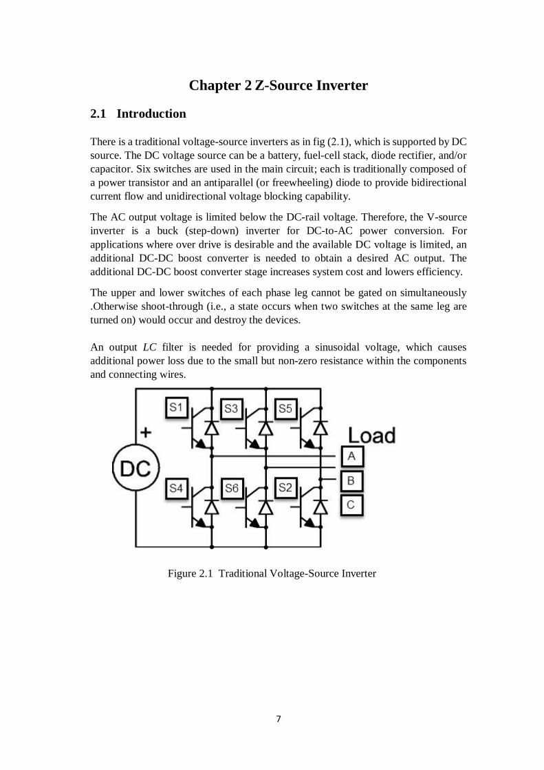
Chapter 2 Z-Source Inverter
2.1 Introduction
There is a traditional voltage-source inverters as in fig ( .8 1), which is supported by DC
source. The DC voltage source can be a battery, fuel-cell stack, diode rectifier, and/or
capacitor. Six switches are used in the main circuit; each is traditionally composed of
a power transistor and an antiparallel (or freewheeling) diode to provide bidirectional
current flow and unidirectional voltage blocking capability.
The AC output voltage is limited below the DC-rail voltage. Therefore, the V-source
inverter is a buck (step-down) inverter for DC-to-AC power conversion. For
applications where over drive is desirable and the available DC voltage is limited, an
additional DC-DC boost converter is needed to obtain a desired AC output. The
additional DC-DC boost converter stage increases system cost and lowers efficiency.
The upper and lower switches of each phase leg cannot be gated on simultaneously
.Otherwise shoot-through (i.e., a state occurs when two switches at the same leg are
turned on) would occur and destroy the devices.
An output LC filter is needed for providing a sinusoidal voltage, which causes
additional power loss due to the small but non-zero resistance within the components
and connecting wires.
Figure 2.1 Traditional Voltage-Source Inverter

8
To overcome the previous problems of the traditional V-source inverters, an
impedance-source power converter (abbreviated as Z-source inverter) was developed
as in Fig. 2.2 which shows the general Z-source inverter structure. It employs a unique
impedance network (or circuit) to couple the inverter main circuit to the power source,
load, or other converter to provide unique features that cannot be observed in the
traditional V- source inverters where a capacitor and inductor are used respectively.
The Z-source inverter overcomes the above-mentioned concept and theoretical barriers
and limitations of the traditional V-source inverter and also provides a novel power
conversion concept.
In Fig. 2.2, a diode is located between a DC source and a two-port network to prevent
DC source from the high network voltage. The two-port network that consists of a
split-inductor L1 and L2 and capacitors C1and C2 connected in X shape is employed
to provide an impedance source (Z-source) coupling the converter (or inverter) to the
DC source, load, or another converter. The DC source/or load can be either a voltage
or a current source/or load. Therefore, the DC source can be a battery, diode rectifier,
thyristor converter, fuel cell, an inductor, a capacitor, or a combination of those.
Switches used in the converter can be a combination of switching devices and diodes
such as the antiparallel combination as shown in Fig. 2.1, the Z-source concept can be
applied to all DC-to-AC, AC-to-DC, AC-to-AC, and DC-to-DC power conversion.
The unique feature of the Z-source inverter is that the output AC voltage can be any
value between zero and infinity regardless of the fuel-cell voltage. That is, the Z-source
inverter is a Buck–Boost inverter that has a wide range of obtainable voltage. The
traditional V- inverters cannot provide such feature.
To describe the operating principle and control of the Z-source inverter in Fig. 2.2, let
us briefly examine the Z-source inverter structure. In Fig. 2.2, the three-phase Z-source
inverter bridge has nine permissible switching states (vectors) unlike the traditional
three-phase V-source inverter that has eight. The traditional three-phase V-source
inverter has six active vectors, when the DC voltage is impressed across the load and
two zero vectors when the load terminals are shorted through either the lower or upper
three devices, respectively. However, the three-phase Z-source inverter bridge has one
extra zero state.
Figure 2.2 Z-source inverter

9
This new extra zero state occurs when the load terminals are shorted through both the
upper and lower devices of any one phase leg (i.e., both devices are gated on), any two
phase legs, or all three phase legs. This shoot-through zero state (or vector) is forbidden
in the traditional V-source inverter, because it would cause a shoot-through. We call
this third zero state (vector) the shoot-through zero state (or vector), which can be
generated by seven different ways: shoot-through via any one phase leg, combinations
of any two phase legs, and all three phase legs. The Z-source network makes the shoot-
through zero state possible. This shoot-through zero state provides the unique buck-
boost feature to the inverter. (Peng, MARCH/APRIL 2003)
The six active vectors for traditional inverter are described in Fig2.3 and Fig2.4 for
square wave and sine wave respectively.
The new extra zero state have 7 statuses could occur with, all these statues and
traditional eight are described in table .2.1
The equivalent circuit of the Z-source inverter as shown in Fig. 2.2 will be as Fig 2.5
when viewed from the DC link. The inverter bridge is equivalent to a short circuit
when the inverter bridge is in the shoot-through zero state, as shown in Fig. 2.7,
whereas the inverter bridge becomes an equivalent current source as shown in Fig. 2.6
when in one of the six active states. Note that the inverter bridge can be also
represented by a current source with zero value (i.e., an open circuit) when it is in one
of the two traditional zero states.
0-60 62-102 102-182 182-002 002-322 322-362 0-60 62-102 102-182 182-002 002-322 322-362
ON S1,S6,S2 S1,S3,S2 S4,S3,S2 S4,S3,S5 S4,S6,S5 S1,S6,S5 S1,S6,S2 S1,S3,S2 S4,S3,S2 S4,S3,S5 S4,S6,S5 S1,S6,S5
OFF S4,S3,S5 S4,S6,S5 S1,S6,S5 S1,S6,S2 S1,S3,S2 S4,S3,S2 S4,S3,S5 S4,S6,S5 S1,S6,S5 S1,S6,S2 S1,S3,S2 S4,S3,S2
VDC+
Vab
VDC-
VDC+
Vbc
VDC-
VDC+
Vca
VDC-
Figure 2.3 Traditional signals for square wave.

10
Table 2.1 Statuses and switches conditions
Active
Vectors On Off
E S1,S6,S2 S4,S3,S5
G S1,S3,S2 S4,S6,S5
C S4,S3,S2 S1,S6,S5
D S4,S3,S5 S1,S6,S2
B S4,S6,S5 S1,S3,S2
F S1,S6,S5 S4,S3,S2
Zero
Vectors On Off
A S4,S6,S2 S1,S3,S5
H S1,S3,S5 S4,S6,S2
Extra
Zero
Vectors
On
Regardless
of which
of other
switches
are off
Z S1,S4 I
Z S3,S6 II
Z S5,S2 III
Z S1,S4,S3,S6 IV
Z S1,S4,S5,S2 V
Z S3,S6,S5,S2 VI
Z S1,S4,S3,S6,S5,S2 VII
Figure 2.4 PWM Signals for sine wave

11
Figure 2.5Equivalent circuit of the Z-source inverter viewed from the DC link.
Figure 2.6Equivalent circuit of Z-Source at one of eight traditional vectors, with I
equal zero at two zero states.

12
2.2 Circuit Analysis and Obtainable Output Voltage
Assuming that the inductors L1 and L2 and capacitors C1 and C2 have the same
inductance and capacitance, respectively, the Z-source network becomes symmetrical.
From the symmetry and the equivalent circuits, we have
VcVcVc 21 VlVlVl 21 (2.1)
Given that the inverter bridge is in the shoot-through zero state for an interval of To ,
during a switching cycle T , and from the equivalent circuit, Fig. 2.7
VcVl VlVcVD VcVD 2 0Vi (2.2)
Now consider that the inverter bridge is in one of the eight nonshoot- through states
for an interval of T1, during the switching cycle T, from the equivalent circuit, Fig. 2.6,
VcVoVl VoVD VoVcVlVcVi 2 (2.3)
Where VO is the DC source voltage and T=TO+T1.
The average voltage of the inductors over one switching period T should be zero in
steady state, from (2.2) and (2.3), thus, we have
Figure 2.5 Equivalent circuit of Z-Source at ninth state or shoot throw state

13
T
VcVoTVcToVl
)(*1* (2.4)
Or ToT
T
Vo
Vc
1
1 (2.5)
Similarly, the average DC-link voltage across the inverter bridge can be found as
follows:
VcVoToT
T
T
VoVcTToviVi
1
1)2(*10* (2.6)
The peak DC-link voltage across the inverter bridge is expressed in (2.3) and can be
rewritten as:
VoBVoToT
TVoVcvlVcvi *
12
(2.7)
Where: 1
21
1
1
T
ToToT
TB (2.8)
B is the boost factor resulting from the shoot-through zero state. The maximum B
(infinity) occurs when To equals 1T ,but the minimum value of B (1) occurs when
To equals Zero.
The peak DC-link voltage vi is the equivalent DC-link voltage of the inverter. On the
other side, the output peak phase voltage from the inverter can be expressed as:
2*
Vi
MacV (2.9)
Where M is the modulation index:
The maximum value of M equals 1 which means the peak of AC output equals half of
DC. The lower the value of M is, the lower the value of the peak of AC is.
Using (2.7), (2.9) can be further expressed as:
2
**Vo
BMacV
(2.10)
The buck–boost factor M.B is determined by the modulation index M and the boost
factor B. The boost factor B as expressed in (2.8) can be controlled by duty cycle of
the shoot-through zero state over the nonshoot-through states of the inverter PWM.
Notice that the shoot-through zero state does not affect the PWM control of the
inverter, because it equivalently produce the same zero voltage to the load terminal.
The available shoot-through period is limited by the zero-state period that is
determined by the modulation index. (Peng, MARCH/APRIL 2003)

14
2.3 Third-Harmonic Injection Pulse Width Modulation
2.3.1 Overview
The third – harmonic PWM is similar to the selected harmonic injection method & it
is implemented in the same manner as sinusoidal PWM. The difference is that the
reference AC waveform is not sinusoidal but consists of both a fundamental
component and a third-harmonic component. As a result, the peak-to-peak amplitude
of the resulting reference function does not exceed the DC supply voltage Vs, but the
fundamental component is higher than the available supply Vs. The reference voltage
Vref is added with signal having frequency three times of fundamental frequency and
the magnitude is 1/6th of the fundamental amplitude. The resultant is then passed
through comparator which compares the modified signal with the carrier.
The presence of exactly the same third-harmonic component in each phase results in
an effective cancellation of the third harmonic component in the neutral terminal, and
the line-to-neutral phase voltages are all sinusoidal with the peak amplitude. By
injecting the third harmonic into the reference voltage signal, the fundamental of the
phase voltage can be increased. The voltage can be increased by harmonic suppression
for the rectifiers as well as inverters. This can be mainly done by injecting the third
harmonic.
2.3.2 Calculation of Optimum Distortion
The generation of the phase voltage waveform having no third harmonics can be
generated by addition of the third harmonics in the sinusoidal reference waveform.
These additions of the various amounts of third, ninth, fifteenth etc. harmonics is used
to produce flat-topped phase waveforms which improves the efficiency of the
inverters. The optimal amount of third harmonic should extend the ratings of all PWM
inverters. The best modification that can be made to the inverter phase output
Figure 2.6 Modulation Signal with third Harmonic Injection

15
waveform is assumed a priori to be the addition of a measure of third harmonics. The
desired waveform of the type
tAty 3sinsin (2.11)
Where A is to be determined for the optimal of Y. The optimal injection is obtained by
differentiating (2.11)
03coscos tAtdt
dy (2.12)
The maxima and minima of the waveform therefore occur at
0cos t and
2/1
12
19cos
A
At (2.13)
0sin t and
2/1
12
31sin
A
At
(2.14)
Manipulating the (11) using identity, we get
3sin4sin31 AAy (2.15)
Substituting the values of sinƟ obtained, we get
Ay
1 and
2/3
12
318
A
AAy
(2.16)
The optimum value of A is that value which minimizes yˆ and can be found by
differentiating the expression for yˆ and equating it to zero. Thus the values of A are
3
1A
and 6
1A
The value of yˆ cannot be greater than unity for this reason the value A= -1/3 is
discarded. The required value of A is therefore 1/6, and the required waveform is
3sin6
1sin u
(2.17)
So the relation 2.17 describes the third harmonic injection. (Dharmadhikari, 2013)
2.4 Control Methods for Z-Source Inverter
2.4.1 Simple Control
The simple control uses two straight lines to control the shoot-through states, as shown
in Fig. 2.9. When the triangular waveform is greater than the upper envelope, Vp, or
lower than the bottom envelope, Vn, the circuit turns into shoot-through state.
Otherwise it operates just as traditional carrier-based PWM. This method is very

16
straightforward; however, the resulting voltage stress across the device is relatively
high because some traditional zero states are not utilized.
2.4.2 Maximum Boost Control
To fully utilize the zero states so as to minimize the voltage stress across the device,
maximum boost control turns all traditional zero states into shoot-through state, as
shown in Fig. 2.10 Third harmonic injection can also be used to extend the modulation
index range Indeed, turning all zero states into shoot-through state can minimize the
voltage stress; however, doing so also causes a shoot-through duty ratio varying in a
line cycle, which causes inductor current ripple. This will require high inductance for
low-frequency or variable-frequency applications
Figure 2.7 Sketch map of simple control
Figure 2.8 Maximum boost control

17
2.4.3 Maximum Constant Boost Control
The sketch map of maximum constant boost control is shown in Fig. 2.12, this method
achieves maximum boost while keeping the shoot-through duty ratio always constant;
thus it results in no line frequency current ripple through the inductors. The sketch map
of maximum constant boost control with third harmonic injection is shown in Fig.2.13.
With this method, the inverter can buck and boost the voltage from zero to any desired
value smoothly within the limit of the device voltage. (Ride & Olszewski, 2005)
Figure 2.9 Maximum boost control with third harmonic injection
Figure 2.12 Maximum constant boost
Figure 2.13 Maximum constant boost control with third harmonic injection

18
2.5 Voltage Stress Comparison of the Control Methods
To examine the voltage stress across the switching devices, an equivalent DC voltage
is introduced. The equivalent DC voltage is defined as the minimum DC voltage
needed for the traditional voltage-source inverter to produce the same output voltage.
The ratio of the voltage stress to the equivalent DC voltage represents the cost that Z-
source inverter has to pay to achieve voltage boost.
The ratios of the voltage stress to the equivalent DC voltage, kstress, for the simple
control, maximum boost control, and maximum constant boost control are summarized
as follows:
Kstress =2-G
1 for simple control (2.18)
Kstress =
33-
G
1 for maximum boost (2.19)
Kstress = 3 -G
1 for maximum constant boost (2.20)
where G is the voltage gain defined as
2/dc
AC
V
VBMG (2.21)
Where ACV is the peak output phase voltage and VDC is the input voltage to the Z-
source inverter. The comparison is shown in Fig.2. 14. In the figure, the voltage stress
of simple control is highest among the three, and the maximum boost achieves the
minimum voltage stress. However, the maximum boost suffers from the six time load
frequency current ripple through the inductor;
Therefore, the maximum constant boost control is the most suitable method for our
application. Also, the maximum constant boost with third harmonic injection seems to
be the better one because it can achieve continuous output voltage variation from zero
to infinity. (Ride & Olszewski, 2005)
Figure 2.10 Voltage stress comparison

19
2.6 Maximum Constant Boost Control
In order to reduce the volume and cost of the Z-source network, we need to eliminate
the low-frequency current ripple by using a constant shoot-through duty ratio. At the
same time, a greater voltage boost for any given modulation index is desired to reduce
the voltage stress across the switches. Fig11.a shows the sketch map of the maximum
constant boost control method, which achieves the maximum voltage gain while
always keeping the shoot-through duty ratio constant. There are five modulation curves
in this control method: three reference signals Va,Vb and Vc and two shoot-through
envelope signals Vp and Vn When the carrier triangle wave is higher than the upper
shoot-through envelope Vp or lower than the bottom shoot-through envelope Vn the
inverter is turned to a shoot-through zero state. In between, the inverter switches in the
same way as in the traditional carrier based PWM control. Because the boost factor is
determined by the shoot-though duty cycle, the shoot-through duty cycle must be kept
the same from switching cycle to switching cycle in order to maintain a constant boost.
The basic point is to get the maximum B while keeping it constant all the time. The
upper and lower envelope curves are periodical and are three times the output
frequency. There are two half-periods for both curves in a cycle.
For the first half-period, [0, π/3] in Fig12, the upper and lower envelope curves can be
expressed by (2.22) and (2.23), respectively
MMVp )3
2sin(31
30
(2.22)
MVn )3
2sin(1
30
(2.23)
For the second half-period [π/3, 2π/3], the envelope curves are expressed by (2.24) and
(2.25), respectively
MVp )sin(2 3
2
3
(2.24)
MMVn 3)sin(2 3
2
3
(2.25)
Obviously, the distance between these two curves determining the shoot-through duty
ratio is always constant for a given modulation index M, that is, M3 . Therefore, the
shoot through duty ratio is constant and can be expressed as :
2
31
2
32 MM
T
To
(2.26)
The boost factor B and the voltage gain G can be calculated as follows
13
1
21
1
M
T
TB
o
(2.27)

20
132/
M
MMB
V
vG
dc
o
(2.28)
The curve of voltage gain versus modulation index is shown in Fig. 2.15. The voltage
gain approaches infinity when M decreases to 3
3
From Fig2.12, we can see that the upper shoot-through envelope is always equal to or
higher than the maximum value of the reference signals, and the lower shoot-through
envelope is always equal to or lower than the minimum value of the reference signals.
Therefore, the shoot-though states only occur during the traditional zero states from
the traditional carrier based PWM control. As a result, this control maintains the output
waveform. It can be easily seen from the above analysis that the shoot-through duty
ratio is always constant. This can be reconfirmed from a different perspective below.
For modulation index M, the maximum active-state duty ratio Da max can be
expressed as
M
tMtM
Da
2
3
2
3
2sinsin
maxmax
(2.29)
Figure 2.11 Voltage gain (MB) versus M

21
Where Da max is the maximum duty ratio of the active states combined in a switching
cycle. In order to keep the active states unchanged while making the shoot-through
duty ratio always constant, the maximum shoot-through duty ratio that can be achieved
is
MDD ao
2
31max1max (2.30)
This is exactly the same as the results shown in (2.26). To summarize, this control
method produces the maximum constant boost while minimizing the voltage stress.
The above-proposed maximum constant boost control (Fig. 2.12) can be implemented
alternatively by using third harmonic injection, A sketch map of the third-harmonic
injection control method is shown in Fig.2.13. A third-harmonic component with 1/6
of the fundamental component is injected to the three phase-voltage references. As
shown in Fig. 2.13, Va reaches its peak value M2
3 while Vb is at its minimum value
M2
3 at
3
. Therefore, a unique feature can be obtained: only two straight lines,
Vp and Vn, are needed to control the shoot-through time with the 6
1 (16%) third
harmonic injection.
From Fig. 2.13, the shoot-through duty ratio can be calculated (2.26)
2
31
2
32 MM
T
To
(2.26)
which is identical to the previously proposed maximum constant boost-control method
shown in Fig. 2.12 Therefore, the voltage gain can also be calculated by the same
equations (2.27) and (2.28). The difference is that the third-harmonic-injection control
method has a larger modulation index M, which increased from 1 to 3
32. The voltage
gain versus M is shown in Fig. 2.8 for the third-harmonic-injection method. The
voltage gain can be varied from infinity to zero smoothly by increasing M from 3
3
to 3
32with shoot through, as shown in the
solid curve, and then decreasing M from 3
32 to zero without shoot through, as shown
in the small dashed curve in Fig. 2.16 (Shen, et al., 2004)

22
Figure 2.12 Voltage gain (MB) verses M in third
harmonic injection

23
Chapter 3
Quasi-Z-Source Inverter

24
Chapter 3 Quasi-Z-Source Inverter
3.1 Introduction
The voltage fed ZSI has some significant drawbacks; namely that the input current is
discontinuous in the boost mode and that the capacitors must sustain a high voltage.
The main drawback of the current fed ZSI is that the inductors must sustain high
currents. Also, control complexity is an issue when the ZSI is used in a back-to-back
configuration due to the coupling of the inverter switching functions. To improve on
the traditional ZSIs, four new quasi-Zsource inverters, qZSIs, have been developed
which feature several improvements and no disadvantages when compared to the
traditional ZSIs. The voltage fed ZSI as well as the two novel voltage fed inverters,
with similar properties to the ZSI, are shown in Figs. 2.2, 3.1, and 3.2, The novel qZSI
topologies shown in Figs. 3.1 and 3.2 The qZSI, shown in Fig. 3.1, when compared to
the ZSI shown in Fig.2.2, features lower DC voltage on capacitor C2 as well as
continuous input current, while the qZSI topology, shown in Fig. 3.2, features lower
DC voltage on capacitors C1 and C2, however, the input current is discontinuous. Also,
due to the input inductor, L1, the qZSI shown in Fig. 3.1 does not require input
capacitance, unlike the ZSI and the qZSI shown in figure 3.2 . (Anderson & Peng,
2008)
Figure 3.1 Voltage Fed qZSI with Continuous Input Current
Figure 3.2 Voltage Fed qZSI with Discontinuous Input Current

25
By using the new quasi-Zsource topology in Fig 3.1, the inverter draws a constant
current from the PV array and is capable of handling a wide input voltage range. It also
features lower component ratings and reduced source stress compared to the traditional
ZSI.
The traditional ZSI, and the qZSI has two types of operational states at the DC side:
the nonshoot-through states (i.e. the six active states and two conventional zero states
of the traditional VSI) and the shoot-through state (i.e. both switches in at least one
phase conduct simultaneously).
In the non-shoot-through states, the inverter bridge viewed from the DC side is
equivalent to a current source. The equivalent circuits of the two states are as shown
in Figs. 3.3 and 3.4 the shoot-through state is forbidden in the traditional VSI, because
it will cause a short circuit of the voltage source and damage the devices. With the
qZSI and ZSI, the unique LC and diode network connected to the inverter bridge
modify the operation of the circuit, allowing the shoot-through state. This network will
effectively protect the circuit from damage when the shoot-through occurs and by
using the shoot-though state, the (quasi-) Z-source network boosts the DC-link voltage.
The major differences between the ZSI and qZSI are:
The qZSI draws a continuous constant DC current from the source while the ZSI draws
a discontinuous current.
The voltage on capacitor C2 is greatly reduced. The continuous and constant DC
current drawn from the source with this qZSI make this system especially well-suited
for PV power conditioning systems.
Figure 3.3 Equivalent circuit of the qZSI in non-shoot-through states

26
Regards to the two fig 3.3&3.4 with Assuming that during one switching cycle, T , the
interval of the shoot through state is To ; the interval of non-shoot-through states is T1
; thus one has T = To + T1 and the shoot through duty ratio, Do= T0 /T . From Fig 3.3
which is a representation of the inverter during the interval of the non-shoot-through
states, T1, one can get
VL1 =Vin −VC1 , VL2 = −VC2 (3.1)
VPN =VC1 − VL2 =VC1 +VC2 Vdiode = 0 . (3.2)
From Fig 3.4 which is a representation of the system during the interval of the shoot-
through states, To , one can get
VL1 =VC2 + Vin , VL2 =VC1 , (3.3)
VPN = 0 Vdiode =VC1 + VC2 . (3.4)
At steady state, the average voltage of the inductors over one switching cycle is zero.
From (3.1), (3.2), one has
0)()( 112
11
T
VVTVVTvV
CininCOLL
Thus
in
O
OC V
TT
TV
1
2
(3.5)
From (3.2), (3.4) and (3.5), the peak DC-link voltage across the inverter bridge is
0)()( 211
22
T
VTVTvV
CCOLL
in
O
C VTT
TV
1
11
Figure 3.4 Equivalent circuit of the qZSI in shoot-through states

27
ininO
in
O
OCCPN BVV
TT
VTT
TVVv
21
1
1
21 (3.6)
Where B is the boost factor of the qZSI. This is also the peak voltage across the diode.
The average current of the inductors L1, L2 can be calculated by the system power
rating P
I L1 = I L2 = I in = P /Vin (3.7)
According to Kirchhoff’s current law and (3.7), we also can get that
IC1 = IC2 = I PN − I L1 I D = 2I L1 − I PN (3.8)
In summary, the voltage and current stress of the qZSI are shown in Table 1. The
stress on the ZSI is shown as well for comparison, where M is the modulation index;
inv is the AC peak phase voltage; P is the system power rating;
m = ToT
T
1
1 ; n =ToT
To
1 ; thus m >1 ;m − n =1;
B = ToT
T
1
1 , thus m + n = B , 1< m < B .
From Table 3.1 we can find that the qZSI inherits all the advantages of the ZSI. It can
buck or boost a voltage with a given boost factor. It is able to handle a shoot through
state, and therefore it is more reliable than the traditional VSI. It is unnecessary to add
a dead band into control schemes, which reduces the output distortion. In addition,
there are some unique merits of the qZSI when compared to the ZSI:
The two capacitors in ZSI sustain the same high voltage; while the voltage on capacitor
C2 in qZSI is lower, which requires lower capacitor rating;
The ZSI has discontinuous input current in the boost mode; while the input current of
the qZSI is continuous due to the input inductor L1, which will significantly reduce
input stress;For the qZSI, there is a common DC rail between the source and inverter,
which is easier to assemble and causes less EMI problems
Table 3.1 Voltage and average current of the qZSI and ZSI network
vL1=vL2 vPN vdiode
T0 T1 T0 T1 T0 T1
ZSI mVin −nVin 0 BVin BVin 0
qZSI mVin −nVin 0 BVin BVin 0
VC1 VC2 inv
ZSI mVin mVin MBVin / 2
qZSI mVin mVin MBVin / 2
Iin =I L1 =IL2 IC1 =IC2 I D
ZSI P /Vin I PN −I L1 2I L1 −I PN
qZSI P /Vin I PN −I L1 2I L1 −I PN

28
If the inverter is operated entirely in the non-shoot-through states (Fig. 3.3) the diode
will conduct and the voltage on capacitor C1 will be equal to the input voltage while
the voltage on capacitor C2 will be zero. Therefore, in vPN=Vin and the qZSI acts as a
traditional VSI:
MV
MV
vinPN
In 22
(3.9)
For SPWM 0≤ M≤1 . Thus when D = 0, Inv is always less than Vin/2 and this is called
the buck conversion mode of the qZSI. By keeping the six active states unchanged
and replacing part or all of the two conventional zero states with shoot-through states,
one can boost VPN by a factor of B , the value of which is related to the shoot-through
duty ratio, as shown in (3.7). This is called the boost conversion mode of the qZSI. (Li,
Anderson, Peng, & Liu, 2009)
The peak AC voltage becomes MBV
MV
vinPN
In 22
(3.10)
3.2 Quasi-Z-Source Inverter Design
The inverter which will be designed here is 10KW rated power with 60Hz 208 V
VL-L (rms). (Li, Anderson, Peng, & Liu, 2009)
This inverter is supplied by DC Voltage source (200-400)VDC , the inverter
parameters are described in table 3.8
Table 3.2The main parameters of inverter
Rated Power 10KW
DC input 200-400 VDC
Output AC Voltage 208V VL-L (rms)
Frequency 60Hz
Carrier Frequency 10 kHz
The maximum voltage gain G will be with 200v DC:
698.1
2
200
2*3
208
2/max
Vdc
VG
AC
.
To get the maximum voltage gain we have to apply the minimum modulation index
M which will be calculated by:
875.1698.1*3
698.1
1max*3
maxmin
G
GM

29
With the same maximum voltage gain G and minimum modulation index M we get
the maximum boost factor B can be calculated by:
939.11875.*3
1
1min*3
1max
MB
The maximum voltage stress on the inverter bridge can be calculated by:
8.387200*939.1max* VdcBVstress
The maximum current in inductor can be calculated by:
AVdc
PIIIin LL 50
200
1000021
The frequency of carrier is 10 KHz so the shoot-through frequency is doubled to 20
kHz so the maximum To can be calculated by:
sec0000242.020000
2
min*31
*2max_
M
To
The inductors in the qZSI network limit the ripples of current during boost conversion
mode, choosing the acceptable peak to peak current ripple rc% to be 20% can be
calculated by:
1050*2.% rc
468.10000242.0000758.
0000758.
1
1
ToT
Tm
468.0000242.0000758.
0000242.
1
ToT
Ton
Hrc
ToVdcmL 355000355.
2*%
max**
These two capacitors absorb the current ripple and limit the voltage ripple on the
inverter bridge and to keep the output voltage sinusoidal. Choosing the acceptable
voltage ripple rv% to be 1% can be calculated by:
2200*01.% rv
FrvB
ToIinC 3110000311.
2*%*
max**2
A model of the qZSI as fig 3.3&3.4 was tested with these parameters in table 3.3:
Table 3.3The parameters of qZSI network
Parameter Value
L 500µH
C 400µF
r 0.235Ω
R 0.07Ω
Lf 1000µH
Cf 100µF
Rload 10Ω

30
Chapter 4
Quasi-Z-Source Inverter
Controller Design

31
Chapter 4 Quasi-Z-Source Inverter Controller Design
4.1 Calculations of M and Do
The controller in this thesis will work in two different methods, the first method is
boosting the DC input voltage less than 294208*2 and the second method will
be bucking when the input voltage above 294208*2 .
The method used in this controller was mamdani with 115 rules as described in
appendix A.
According to these relationships for Boost:
2/Vdc
VG
AC
1*3
G
GM
2
*31
MDo
ToT
Tm
1
1
ToT
Ton
1
mVdcVc 1
nVdcVc 2
1*3
1
MB
VdcBVstress *
According to these relationships for Buck:
3*
2*208*2
VdcMG
0Do
VdcVc 1
02 Vc

32
And choosing samples of VDC ; values below than 294208*2 the inverter must
work in boost and values which above 294 must work in buck with these values in
table 4.1:
Table 4.1Samples of VDC
VDC M Do Mode
200 0.875 0.242 Boost
220 0.922 0.201 Boost
240 0.953 0.174 Boost
260 1.016 0.120 Boost
280 1.102 0.046 Boost
292 1.146 0.007 Boost
294 1.150 0 Buck
296 1.148 0 Buck
312 1.089 0 Buck
332 1.023 0 Buck
352 0.965 0 Buck
372 0.913 0 Buck
392 0.866 0 Buck
For boosting seven samples of vDC from 200 to 292 v and the values of modulation
Index M and Duty ratio Do was calculated.
For Bucking the only values must calculated is only modulation index M and fixed
zero value for duty ratio Do; another seven samples was chosen from 294 to 392.
4.2 Fuzzy Controller Memberships
4.2.1 Introduction
In this thesis the controller have three inputs and two outputs, the three inputs was
chosen as below:
VDC: This input take care of the statues of source voltage, so that the controller must
take the decision for work as boost or buck and the values of M and Do.
IDC: This input take care of the statues of current in inductor in quasi-Z-source
network, so the controller give the value of Do to limit the current as possible.
Vc1: The value of Vc1 give the reached value of boosting voltage, so the controller
give values of M and Do to keep it 294 if input VDC is below the 294,and if its above
this input is not considered.
The two outputs of controller are used in this thesis separately to control the output
voltage and current in inductor, these two outputs are:
33
M: modulation index M can be 3
3 to
3
32 in boosting; the less M in boosting give
the max boost and an be from 0 to 1 in bucking; the maximum M in buck give the
minimum buck. (Shen, et al., 2004)
Do: duty ratio Do have a job just in boosting and can control the current in inductor
but must keep the relation )1(3
2DoM to avoid distortion of output signal. (Li,
Jiang, Cintron-Rivera, & Peng, 2013)
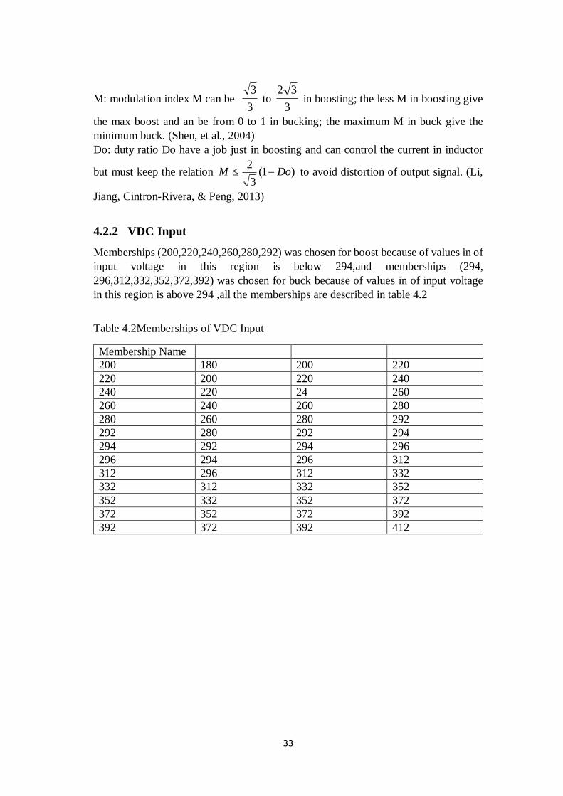
4.2.2 VDC Input
Memberships (200,220,240,260,280,292) was chosen for boost because of values in of
input voltage in this region is below 294,and memberships (294,
296,312,332,352,372,392) was chosen for buck because of values in of input voltage
in this region is above 294 ,all the memberships are described in table 4.2
Table 4.2Memberships of VDC Input
Membership Name
200 180 200 220
220 200 220 240
240 220 24 260
260 240 260 280
280 260 280 292
292 280 292 294
294 292 294 296
296 294 296 312
312 296 312 332
332 312 332 352
352 332 352 372
372 352 372 392
392 372 392 412

34
All the memberships are trimf, the narrowest membership is 294 because the centre
of this membership is 294 the critical point in this input as described in fig 4.1.
4.2.3 IDC Input
The aim of choosing this input is keeping the current in inductor the minimum as
possible as I can to reduce the radius of inductor wire, the memberships as described
in table 4.3.
Table 4.3Memberships of IDC Input
Membership Name
292(34.25) -5 0 34.25 35.71
280(35.714) 34.25 35.71 38.46
260(38.462) 35.71 38.46 41.67
240(41.667) 38.46 41.67 45.45
220(45.455) 41.67 45.45 50
200(50) 45.45 50 80 85
The memberships ( 292(34.25) and 200(50)) are trampf because the lowest current
value of 10kw load is at 292 volt with 34.5 amp and the highest current value of 10kw
load is at 200 volt with 50 amp.
Figure 4.1 Memberships Functions of VDC Input

35
The other memberships are rtimf as fig 4.2.
4.2.4 Vc1 Input
The aim of choosing this input is keeping the output voltage constant to 294 volt
whatever the input voltage within the boost range of (200-294) ,the memberships are
described in table 4.4.
Table 4.4Memberships of Vc1 Input
Membership Name
290 96 100 290 294
294 290 294 298
298 294 298 396 400
The memberships ( 290 and 298) are trampf because the input value of rang of 290
membership make the controller work in boosting and the input value of range of 298
membership make the controller work in bucking.
The other membership 294 is rtimf because this is the critical membership as fig 4.3.
Figure 4.2 Memberships Functions of IDC Input

36
4.2.5 M output
The aim of choosing this input is keeping the output voltage constant to 294 volt
whatever the input voltage within the boost range of (200-400).
The memberships (2,4,5,7,10) in table 4.5 are used in boosting and memberships
(1,3,6,8,9,12) in table 4.5 are used in bucking .
Table 4.5Memberships of M Output
# Membership
Name
1 392(0.866) 0.857 0.866 0.875
2 200(0.875) 0.866 0.875 0.913
3 372(0.913) 0.875 0.913 0.922
4 220(0.922) 0.913 0.922 0.954
5 240(0.953) 0.922 0.954 0.965
6 352(0.965) 0.954 0.965 1.016
Figure 4.3 Memberships Functions of Vc1 Input

37
7 260(1.016) 0.965 1.016 1.023
8 332(1.023) 1.016 1.023 1.089
9 312(1.089) 1.023 1.089 1.102
10 280(1.102) 1.089 1.102 1.146
11 292(1.146) 1.102 1.146 1.148
12 296(1.148) 1.146 1.148 1.150
13 294(1.150) 1.148 1.150 1.152
All the memberships in table 4.5 are trimf, described in fig 4.4.
4.2.6 Do Output
The aim of choosing this output is keeping the current in inductor to the minimum as
possible as I can to reduce the radius of inductor wire, the memberships as described
in table 4.6.
Table 4.6Memberships of Do Output
Membership Name
0 -0.007 0 0.007
292(0.007) 0 0.007 0.046
280(0.046) 0.007 0.046 0.120
260(0.120) 0.046 0.120 0.174
240(0.174) 0.120 0.174 0.201
220(0.201) 0.174 0.201 0.242
200(0.242) 0.201 0.242 0.283
Figure 4.4 Memberships Functions of M Output
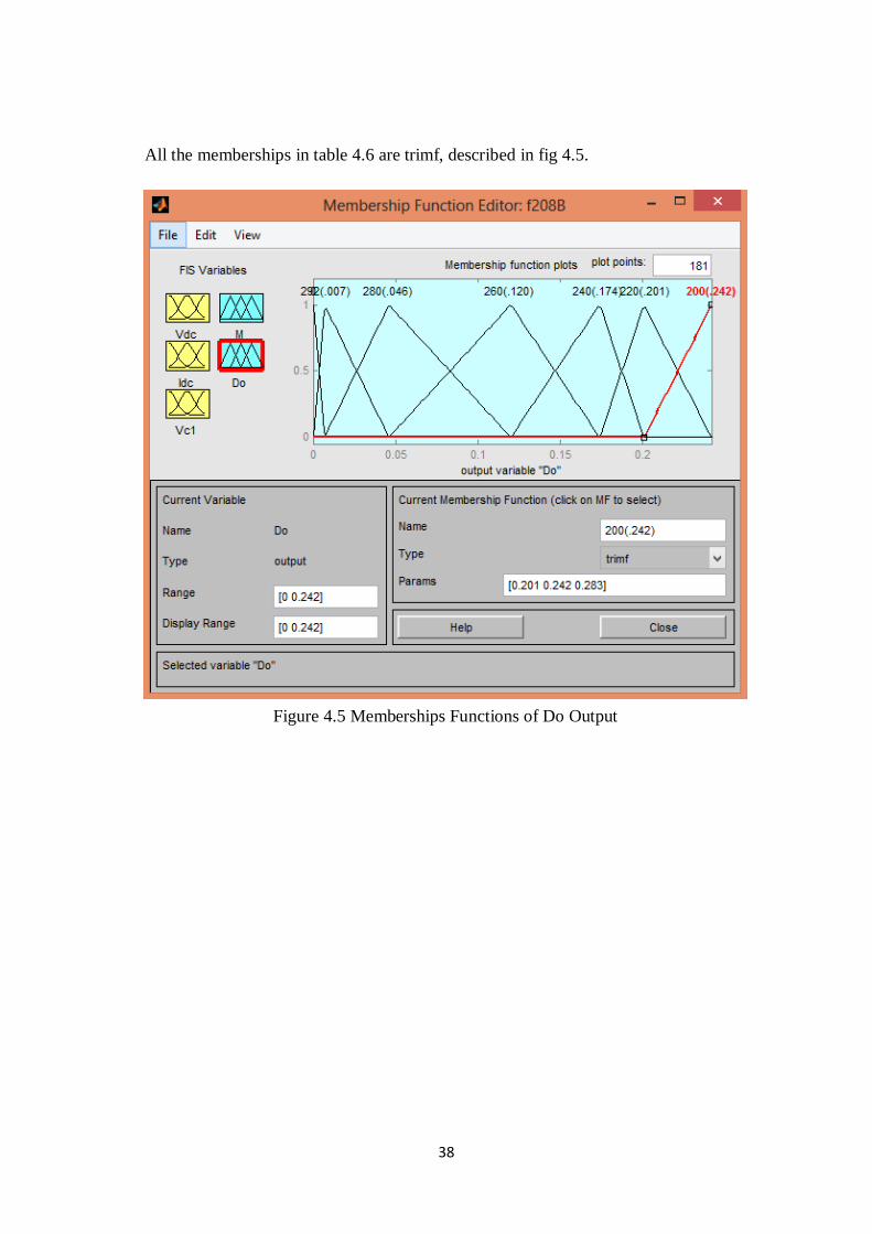
38
All the memberships in table 4.6 are trimf, described in fig 4.5.
Figure 4.5 Memberships Functions of Do Output

39
4.3 Surfaces
M Output
Do Output
Figure 4.6 Surface for M Output
Figure 4.7 Surface for Do Output

40
4.4 Simulink Model
In this thesis Matlab Simulink used for simulation because of its wide element exist in
Simulink libraries; the Simulink model as shown in fig 4.8 consist of:
Variable DC Block :is a sin wave source shifted 200 in x axis and peak to peak 200
also with 5 Hz frequency connected to (controlled voltage source) to give variable DC
source [200-400].
Quasi Z Source: this block contain quasi-Z-Source network as in fig 3.1 with values
of L,C,r,R and Rload as in table 3.3.
Universal Bridge: this is 3 bridge arms of IGBT to work as switches for three phase
inverter switches.
Filter: This filter is LC filter with values of Lf and Cf as in table 3.3.
Fuzzy Logic Controller: This Fuzzy controller contain the fuzzy system described in
section 4.2.
Scope: this Scope consist of 6 axis
DC Input
DC Input Current.
Three-phase voltage waves.
Three-phase current waves.
Voltage stress cross switches.
Output voltage line-line rms.
Pulses: This block is described in fig4.9 and contain.
Three sine wave with third harmonic injection reference signals, the phase shift
between each other is 120 degree and the peak value changes as M change, the peak
of third harmonic injected signal is M2
3 as mentioned in page 21 ,so if the
M=1.15 the peak of reference will be 1.
Triangular wave generator with 10KHz frequency as carrier signal and fixed peak
value of 1.
Comparators to choose the system will operate in boosting or bucking.

41
Figure 4.8 Simulink Model of all system

42
Figure 4.9 Pulses Block

43
4.5 Results
The simulation for the designed Fuzzy Controller described in section 4.2 in the system
designed in table 3.3 with applying variable DC input (200-400)v is shown in fig 4.10
.It is clear that the output voltage rms is in range of (206-209)rms L-Line.
In fig 4.10 the system simulated for 0.2 second as one period of the DC source block,
the voltage in 0 s is 200 v and in 0.1 sec is 400 and go back to 200 by 0.2sec.
Changing in DC input keep the rms value of output rms (206-209) volt with fixed load
10 KW.
Value of current is inversely proportional to input DC voltage except in the first of
operating the energy absorbed from source is more than 10KW it about 15KW.
The output signal is pure sine wave in voltage and current.
The voltage stress is about 400 and the calculated in page 28 was 387 v
I tried the same system with fixed input DC voltage to 200 v for 0.025 sec with fuzzy
controller in fig 4.11 ,and no controller in fig 4.12 with fixed values of M and Do as
calculated in page 28 and 31 M= 0.875 and Do =0.242.
The result of fuzzy controlled system was in fig 4.11 and the maximum DC current
was 75 A which mean the system with load 10KW absorbs 15Kw for for a little while,
but the no fuzzy controlled system the maximum DC current was 145 A absorbs 29Kw,
these advantage accrued by controlling M and Do indecently.
The another point I noticed is voltage stress ,in non-controlled system with 200 v DC
input the maximum voltage stress was 500 v but in fuzzy controlled one was 400v.
Figure 4.10 Results of Variable VDC Input (200-400)

44
By the designed fuzzy controller the reduced current in inductor mean reducing the
cross section in inductor wire and reducing weight and volume of device, and of course
increasing the efficiency of inverter in solar systems.
Reducing voltage stress mean cheaper switches and less heat in device.
Figure 4.11 Result of Fixed Input 200 V DC with fuzzy controller.
Figure 4.12 Result of Fixed Input 200 V DC without controller

45
Chapter 5
Conclusion and Future
Research

46
Chapter 5 Conclusion and Future Research
5.1 Conclusions
Nowadays electrical energy converting plays an important role in industries and daily
life, especially DC-AC inverters, because of existing many DC sources like batteries,
solar panels and super capacitors; besides to motor inverters applications.
Z-source inverter discussed briefly in this thesis with its ability to work buck & boost
and overcome regular inverter limitations.
To overcome Z-Source inverter disadvantages quasi-Z-source inverter described and
analysed.
Related on previous background 10KW quasi-Z-Source designed and controlled by
fuzzy controller.
In this research I applied Fuzzy controller with three inputs (VDC,IDC and Vc1) and
two outputs (M and Do) ,this fuzzy controller contain 115 rule with mamdani method.
Fuzzy controller controlled the main input parameters of quasi-z-source M&Do
separately, with this technique I could control the input current DC and the output
voltage AC separately, in the simulation result it clear that the output voltage was
constant to 208 VL-L rms with wide range of input DC voltage (200-400)v, and I could
minimize the current in inductor to half which minimize the size and weight of device.
5.2 Future Work
In this thesis mamdani method was used in fuzzy controller, it will be very important
and helpful to compare it with sugeno method.
The load here in this thesis was resistive load, it can be changed to variable power
factor load and improve controller and filter design to achieve the perfect results.

47
References
Anderson, J., & Peng, F. Z. (2008, June). Four Quasi-Z-Source Inverters. IEEE
PESC, 2743-2749.
Dharmadhikari, P. S. (2013). Comparison of Full Bridge Voltage Source Inverter
with Diffrent PWM Techniques. National Confrence on Innovative
Paradigms in Engineering & Technology, 25-30.
Ge, B., Abu-Rub, H., Peng, F. Z., Lei, Q., Almeida, A. T., Ferreira, F. J., . . . Liu, Y.
(2013, October). An Energy-Stored Quasi-Z-Source Inverter for Application
to Photovoltaic Power System. IEEE Transactions on Industrial Electronics,
60(10), 4468-4481.
Husodo, B. Y., Ayoub, S. M., Anwari, M., & Taufik. (2013, May). Simulation of
Modified Simple Boost Control for Z-Source Inverter. Intrnational Journal of
Automation and Power Engineering, 2(4), 57-64.
Laxmi, G. J., & Ro, J. R. (2013, November). Multi Switching Techniques of Z-
Source Inverter based PMSM Drive. International Journal of Engineering
Research & Technology, 2(11), 4215-4223.
Li, X., Yan, Z., Pan, K., Ma, C., & Qi, H. (2013). The Control Technology Research
of the Z-Source Three Phase Four Bridge Arm Inverter. Energy and Power
Engineering, 733-739.
Li, Y., Anderson, J., Peng, F. Z., & Liu, D. (2009). Quasi-Z-Source Inverter for
Photvoltaic Power Generation Systems. 24th IEEE APEC, 918-924.
Li, Y., Jiang, S., Cintron-Rivera, J. G., & Peng, F. Z. (2013, April). Modeling and
Control of Quasi-Z-Source Inverter for Distributed Generation Applications.
IEEE Transactions on Industrial Electronics, 60(4), 1532-1541.
Liu, Y., Gel, B., & Abu-Rub, H. (2013). Modelling and Controller Design of Quasi-
Z-Source Cascaded Multilevel Inverter-Based Three Phase Grid Tie
Photovoltaic Power System. Rewable Power Generation, 8(8), 925-936.
Neeraj, M. K., Kumar, C. L., & J, S. H. (2015). Three Phase Voltage Source Inverter
for Front End Rectifier Fed to AC-Motor Drive Using Matlab. Intrnational
Journal of Engineering Sience and Innovative Technology, 4(3), 221-226.
Penchalababu, V., Chandarakala, B., & Karismna, G. (2012, June). A survey on
Modified Simple Boost Control for Z-Source Inverter. International Journal
of Engineering and Advanced Technology, 1(5), 556-562.
Peng, F. Z. (MARCH/APRIL 2003). Z-Source Inverter. IEEE TRANSACTIONS ON
INDUSTRY APPLICATIONS, VOL. 39, NO. 2, 39(2), 504-510.
Ride, O., & Olszewski, M. (2005). Shoot-Through PWM Control. In Z-Source
Inverter for Fuel Vechicles (pp. 39-45).

48
Sathya, S., & Karthikeyan, C. (2013, July). Fuzzy Logic Based Z-Source Inverter for
Hybrid Energy Resources. Intternational Journal of Engineering Science and
Innovative Technology, 2(4), 57-63.
Shen, A. W., Pham, C.-T., Dzung, P. Q., Anh, N. B., & Viet, L. H. (2012, August).
Using Fuzzy Logic Self-Tuning PI Gain Controller Z-Source Inverter in
Hubrid Electric Vechicles. Irternational Journal of Engineering and
Technolgy, 4(4), 382-387.
Shen, M., Wang, J., Joseph, A., Peng, F. Z., Tolbert, L. M., & Adams, D. J. (2004).
Maximum Constant Boost Control of the Z-Source Inverter. IAS IEEE, 142-
147.
Shen, M., Wang, J., Peng, F. Z., Tolbert, L. M., & Adams, D. J. (2006, May/June).
Constant Boost Control of the Z-Source Inverter to Minmize Current Ripple
and Voltage Stress. IEEE Transaction on Industry Applications, 42(3), 770-
778.
Shete, P. S., Kanojiya, R. G., & Maurya, N. S. (2012). Performance of Sinusoidal
Pulse Width Modulation based Three Phase Inverter. International Confrance
on Emerging Frotiers in Technology for Rural Area, 22-26.
Siwakoti, Y. P., Peng, F. Z., Blaabjerg, F., Loh, P. C., & Town, G. E. (2015,
February). Impedance-Source Networks for Electric Power Conversion Part
I:Review of Control and Modulation Techniques. IEEE Transaction on
Power Electronics, 30(2), 699-716.
Siwakoti, Y. P., Peng, F. Z., Blaabjerg, F., Loh, P. C., Town, G. E., & Yang, S.
(2015, April). Impedance-Source Networks for Electric Power Conversion
Part II:Review of Control and Modulation Techniques. IEEE Transactions on
Power Electronics, 30(4), 1887-1906.
Suresh, L., Kumar, G. N., & Sudarsan, M. V. (2012). Modulation and Simulation of
Z-Source Inverter. Vadlamudi: Selected Works of suresh l.
Vijayabalan, R., & Ravivarman, S. (2012, December). Z-Source Inverter for
Photovoltaic System with Fuzzy Logic Controller. International Journal of
Power Electronics and Drive System, 2(4), 371-379.

49
Appendices
Appendix A
Table Appendix. 1 Fuzzy Rules
VDC IDC Vc1 M Do
1 200 292(34.25) 290 200(0.875) 200(0.242)
2 200 292(34.25) 294 200(0.875) 200(0.242)
3 200 292(34.25) 298 220(0.922) 200(0.242) 4 200 280(35.714) 290 200(0.875) 200(0.242)
5 200 280(35.714) 294 200(0.875) 200(0.242) 6 200 280(35.714) 298 220(0.922) 200(0.242)
7 200 260(38.462) 290 200(0.875) 200(0.242)
8 200 260(38.462) 294 200(0.875) 200(0.242) 9 200 260(38.462) 298 220(0.922) 200(0.242)
10 200 240(41.667) 290 200(0.875) 200(0.242) 11 200 240(41.667) 294 200(0.875) 200(0.242)
12 200 240(41.667) 298 220(0.922) 200(0.242) 13 200 220(45.455) 290 200(0.875) 200(0.242)
14 200 220(45.455) 294 200(0.875) 200(0.242)
15 200 220(45.455) 298 220(0.922) 200(0.242) 16 200 200(50) 290 200(0.875) 0
17 200 200(50) 294 200(0.875) 200(0.242) 18 200 200(50) 298 220(0.922) 200(0.242)
19 220 292(34.25) 290 220(0.922) 220(0.201) 20 220 292(34.25) 294 220(0.922) 220(0.201)
21 220 292(34.25) 298 240(0.953) 220(0.201)
22 220 280(35.714) 290 220(0.922) 220(0.201) 23 220 280(35.714) 294 220(0.922) 220(0.201)
24 220 280(35.714) 298 240(0.953) 220(0.201) 25 220 260(38.462) 290 220(0.922) 0
26 220 260(38.462) 294 220(0.922) 220(0.201)
27 220 260(38.462) 298 240(0.953) 220(0.201) 28 220 240(41.667) 290 220(0.922) 0
29 220 240(41.667) 294 220(0.922) 220(0.201) 30 220 240(41.667) 298 240(0.953) 220(0.201)
31 220 220(45.455) 290 220(0.922) 0
32 220 220(45.455) 294 220(0.922) 0
33 220 220(45.455) 298 240(0.953) 0
34 220 200(50) 290 220(0.922) 0
35 220 200(50) 294 220(0.922) 0
36 220 200(50) 298 240(0.953) 0
37 240 292(34.25) 290 240(0.953) 240(0.174)
38 240 292(34.25) 294 240(0.953) 240(0.174)
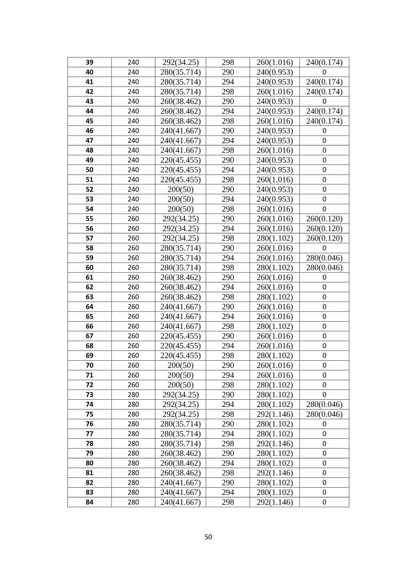
50
39 240 292(34.25) 298 260(1.016) 240(0.174)
40 240 280(35.714) 290 240(0.953) 0
41 240 280(35.714) 294 240(0.953) 240(0.174)
42 240 280(35.714) 298 260(1.016) 240(0.174) 43 240 260(38.462) 290 240(0.953) 0
44 240 260(38.462) 294 240(0.953) 240(0.174)
45 240 260(38.462) 298 260(1.016) 240(0.174) 46 240 240(41.667) 290 240(0.953) 0
47 240 240(41.667) 294 240(0.953) 0
48 240 240(41.667) 298 260(1.016) 0
49 240 220(45.455) 290 240(0.953) 0
50 240 220(45.455) 294 240(0.953) 0
51 240 220(45.455) 298 260(1.016) 0
52 240 200(50) 290 240(0.953) 0
53 240 200(50) 294 240(0.953) 0
54 240 200(50) 298 260(1.016) 0
55 260 292(34.25) 290 260(1.016) 260(0.120)
56 260 292(34.25) 294 260(1.016) 260(0.120) 57 260 292(34.25) 298 280(1.102) 260(0.120)
58 260 280(35.714) 290 260(1.016) 0
59 260 280(35.714) 294 260(1.016) 280(0.046) 60 260 280(35.714) 298 280(1.102) 280(0.046)
61 260 260(38.462) 290 260(1.016) 0
62 260 260(38.462) 294 260(1.016) 0
63 260 260(38.462) 298 280(1.102) 0
64 260 240(41.667) 290 260(1.016) 0
65 260 240(41.667) 294 260(1.016) 0
66 260 240(41.667) 298 280(1.102) 0
67 260 220(45.455) 290 260(1.016) 0
68 260 220(45.455) 294 260(1.016) 0
69 260 220(45.455) 298 280(1.102) 0
70 260 200(50) 290 260(1.016) 0
71 260 200(50) 294 260(1.016) 0
72 260 200(50) 298 280(1.102) 0
73 280 292(34.25) 290 280(1.102) 0
74 280 292(34.25) 294 280(1.102) 280(0.046)
75 280 292(34.25) 298 292(1.146) 280(0.046) 76 280 280(35.714) 290 280(1.102) 0
77 280 280(35.714) 294 280(1.102) 0
78 280 280(35.714) 298 292(1.146) 0
79 280 260(38.462) 290 280(1.102) 0
80 280 260(38.462) 294 280(1.102) 0
81 280 260(38.462) 298 292(1.146) 0
82 280 240(41.667) 290 280(1.102) 0
83 280 240(41.667) 294 280(1.102) 0
84 280 240(41.667) 298 292(1.146) 0

51
85 280 220(45.455) 290 280(1.102) 0
86 280 220(45.455) 294 280(1.102) 0
87 280 220(45.455) 298 292(1.146) 0
88 280 200(50) 290 280(1.102) 0
89 280 200(50) 294 280(1.102) 0
90 280 200(50) 298 292(1.146) 0
91 292 292(34.25) 290 292(1.146) 0
92 292 292(34.25) 294 292(1.146) 292(0.007)
93 292 292(34.25) 298 292(1.146) 292(0.007) 94 292 280(35.714) 290 292(1.146) 0
95 292 280(35.714) 294 292(1.146) 0
96 292 280(35.714) 298 292(1.146) 0
97 292 260(38.462) 290 292(1.146) 0
98 292 260(38.462) 294 292(1.146) 0
99 292 260(38.462) 298 292(1.146) 0
100 292 240(41.667) 290 292(1.146) 0
101 292 240(41.667) 294 292(1.146) 0
102 292 240(41.667) 298 292(1.146) 0
103 292 220(45.455) 290 292(1.146) 0
104 292 220(45.455) 294 292(1.146) 0
105 292 220(45.455) 298 292(1.146) 0
106 292 200(50) 290 292(1.146) 0
107 292 200(50) 294 292(1.146) 0
108 292 200(50) 298 292(1.146) 0
109 294 - - 294(1.150) 0
110 296 - - 296(1.148) 0
111 312 - - 312(1.089) 0
112 332 - - 332(1.023) 0
113 352 - - 352(0.965) 0
114 372 - - 372(0.913) 0
115 392 - - 392(0.866) 0


![Chapter 3: Fuzzy Rules & Fuzzy Reasoning513].pdf · CH. 3: Fuzzy rules & fuzzy reasoning 1 Chapter 3: Fuzzy Rules & Fuzzy Reasoning ... Application of the extension principle to fuzzy](https://img.pdfslide.us/doc/110x75/5b3ed7b37f8b9a3a138b5aa0/chapter-3-fuzzy-rules-fuzzy-513pdf-ch-3-fuzzy-rules-fuzzy-reasoning.jpg)


![QUASI-BIGEBRES DE LIE ET ALGEBRES QUASI-BATALIN ...streaming.ictp.it/preprints/P/99/174.pdf3 Quasi-bigebres de Lie Les quasi-bigebres de Lie [6] (appelees quasi-bigebres jacobiennes](https://img.pdfslide.us/doc/110x75/60aa5fd4a787df4f051abfc1/quasi-bigebres-de-lie-et-algebres-quasi-batalin-3-quasi-bigebres-de-lie-les.jpg)