Embed Size (px)
Citation preview
www.furuno.com
FURUNO GNSS Receiver
Model GT-87
Hardware Specifications
(Document No. SE16-410-013-01)
GT-87 Hardware Specifications
SE16-410-013-01
IMPORTANT NOTICE No part of this manual may be reproduced or transmitted in any form or by any means, electronic or mechanical, including photocopying and recording, for any purpose without the express written permission of the publisher, FURUNO ELECTRIC CO., LTD. FURUNO ELECTRIC CO., LTD. All rights reserved.
Any information of this documentation shall not be disclosed to any third party without permission of the publisher, FURUNO ELECTRIC CO., LTD.
FURUNO ELECTRIC CO., LTD. reserves the right to make changes to its products and specifications without notice. All brand and product names are registered trademarks, trademarks or service marks of their respective holders. The following satellite systems are operated and controlled by the authorities of each government.
- GPS(USA) - GLONASS (Russia) - Galileo(Europe) - QZSS(Japan) - SBAS(USA: WAAS, Europe: EGNOS, Japan: MSAS)
Thus FURUNO is not liable for the degradation of the above systems so therefore FURUNO cannot guarantee specification based on their conditions. User is expected to be familiar with the System and make full use of it with their own responsibility.
GT-87 Hardware Specifications
SE16-410-013-01
Revision History
Version Changed contents Date
0
Changed document number from G13-000-10-015-3
2016.12.13
Table 2.1—Corrected the operational limit of altitude.
Table 3.1—Corrected the condition.
Table 6.2—Added Notes for rising slew rate of VCC and VBK. Updated the VCC current consumption.
Updated Figure 6.1
Table 6.3—Added Notes for equivalent pull-up/pull-down resistor
Added Section 6.3.2
Table 6.3, Table 6.4—Remove the condition “TA=25°C, unless otherwise stated”
Updated Figure 6.3 and Table 6.5
Table 6.6, Table 6.7—Corrected the symbols
Table 6.8—Added signs for deviation error
Table 6.9—Changed Amplifier gain 1 spec and Amplifier NF spec.
Table 8.1—Added RESERVED pins. Corrected the equivalent circuit for VCC_RF.
Section 9.1—Added the height Y
Figure 10.1—Corrected the recommended land pattern
Section 10.2.1—Corrected the example of connection with active antenna
Chapter 11—Added descriptions for marking specification
Table 13.1—Corrected the specified classification temperature
1 Chapter 4—Corrected the GCLK frequency. 2017.08.23
GT-87 Hardware Specifications
SE16-410-013-01
Table of Contents
1 Outline ······················································································································ 1
2 GNSS General Specifications ······················································································· 1
3 GNSS General Performance ························································································· 2
4 Functional Overview ··································································································· 3
5 I/O Signal Description ·································································································· 4
6 Electrical Characteristics ····························································································· 5 Absolute Maximum Rating ····························································································· 5 6.1 Power Supply ··············································································································· 6 6.2 Interface ······················································································································ 7 6.3
6.3.1 Interface Signal ······································································································· 7 6.3.2 Precaution on Using the Input Pin with Pull-up Resistor ·············································· 7 Reset ··························································································································· 7 6.4
6.4.1 Internal Power-on Reset ··························································································· 7 6.4.2 External Reset ········································································································ 8 UART Wake-up Timing after Reset ·················································································· 9 6.5
6.5.1 Without External Reset ···························································································· 9 6.5.2 With External Reset ································································································· 9 6.5.3 Baud Rate Setting ································································································· 10 Recommended GNSS Antenna ······················································································ 10 6.6
6.6.1 Active Antenna ····································································································· 10 6.6.2 Passive Antenna ··································································································· 10
7 Environmental Specifications ····················································································· 11
8 Equivalent Circuit ····································································································· 11
9 Mechanical Specifications ·························································································· 13 Package Dimension ····································································································· 13 9.1 Electrode ···················································································································· 13 9.2 Weight ························································································································ 13 9.3 Pin Position List ·········································································································· 14 9.4
10 Reference Design ··································································································· 14 Recommended Land Pattern ························································································· 14 10.1 Example of Connection ································································································ 15 10.2
10.2.1 With Active Antenna ······························································································ 15 10.2.2 With Passive Antenna ···························································································· 16
11 Marking ················································································································ 17
12 Handling Precaution ······························································································· 18
13 Solder Profile ········································································································ 19 Reflow Profile ·············································································································· 19 13.1 Precaution about Partial Heating with the Way except Reflow ··········································· 20 13.2
14 Special Instruction ································································································· 20 Electronic Component ·································································································· 20 14.1 ESD Damage ··············································································································· 20 14.2 RoHS ·························································································································· 20 14.3
15 Reference Documents ···························································································· 20
GT-87 Hardware Specifications
SE16-410-013-01
1
1 Outline
GT-87 is a stand-alone, complete GNSS timing receiver module. It is designed to provide accurate timing pulse (PPS) to customers’ various applications that are required to be synchronized to UTC time. Main features are as follows: Supports GPS, GLONASS, SBAS, QZSS and Galileo
1) with the latest eRideOPUS 7 monolithic GNSS
receiver chip. Provides highly accurate PPS signal for various synchronization application with outputting PVT (Position,
Velocity and Time) information through serial communication channel. Supports firmware update through serial communication channel. Fully integrated GNSS firmware executes acquisition, tracking, navigation and data output for multiple
constellations. Active Anti-jamming technology removes up to 8 CW jammers efficiently. Multi path mitigation technology maintains high accuracy even in an urban canyon. Works in both Autonomous mode and Assisted mode. GNSS high sensitivity enables to use at deep indoor environment. Both active and passive antenna usable. Low profile, small SMT package reducing foot print on PCB and assembly cost. Notes: 1) For Galileo reception, firmware update is required.
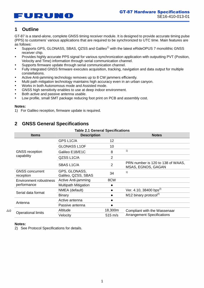
2 GNSS General Specifications
Table 2.1 General Specifications
Items Description Notes
GNSS reception capability
GPS L1C/A 12
GLONASS L1OF
10
Galileo E1B/E1C 8 1)
QZSS L1C/A
2
SBAS L1C/A 2 PRN number is 120 to 138 of WAAS, MSAS, EGNOS, GAGAN
GNSS concurrent reception
GPS, GLONASS, Galileo, QZSS, SBAS
34 1)
Environment robustness performance
Active Anti-jamming 8CW
Multipath Mitigation ●
Serial data format NMEA (default)
● Ver. 4.10, 38400 bps
2)
Binary ● M12 binary protocol2)
Antenna Active antenna ●
Passive antenna ●
Operational limits Altitude 18,300m Compliant with the Wassenaar
Arrangement Specifications Velocity 515 m/s
Notes: 2) See Protocol Specifications for details.
△0
GT-87 Hardware Specifications
SE16-410-013-01
2
3 GNSS General Performance
Table 3.1 General Performance TA=25°C
Items Description Notes
TTFF
Hot Outdoor
<5 s These are specified with the measurement platform shown in Figure 3.1. Simulator output level is set to -130 dBm.
Warm Outdoor 35 s
Cold Outdoor 35 s
GPS sensitivity
Tracking -161 dBm
These are specified with the measurement platform shown in Figure 3.1.
Hot Acquisition -161 dBm
Cold Acquisition -147 dBm
Reacquisition -161 dBm
GLONASS sensitivity
Tracking -157 dBm
Hot Acquisition -157 dBm
Cold Acquisition -143 dBm
Reacquisition -157 dBm
Position accuracy Horizontal Outdoor
2.5m CEP GPS only Open sky 24 hours with recommended antenna
2.0m CEP GPS, GLONASS and SBAS Open sky 24 hours with recommended antenna
PPS accuracy 1σ 15 ns Open sky, static with recommended antenna
Multi-GNSS Simulator
GSS6700
External LNA
Gain: 30.4dB
NF: 0.6dB
Including Cable
Loss
GT-87
Evaluation Board
LNA Setting:
Low Gain
PC
Figure 3.1 Measurement Platform
△0
GT-87 Hardware Specifications
SE16-410-013-01
3
4 Functional Overview
GT-87 is a stand-alone, complete GNSS timing receiver module that can provide accurate PPS signal with GNSS PVT (Position, Velocity & Time) information through serial communication channel. The key device inside is eRideOPUS 7, the latest monolithic GNSS receiver chip that contains ARM9
TM processor for signal
tracking and processing, high performance integrated LNA, PLL Synthesizer, Down-converter, ADC and DSP. GT-87 also contains Flash ROM for firmware and data storage, TCXO for reference clock, 32 kHz crystal for RTC (Real time clock), L1 band SAW filter and power-on reset circuit. The block diagram is shown in Figure 4.1.
PPS pin provides accurate timing pulse which is synchronized to UTC (GPS) time system. The frequency of PPS signal is configurable by commands through serial communication channel (RXD1). Also GCLK pin provides clock output synchronized to PPS. The frequency of GCLK is configured by serial command from 4 kHz up to 40 MHz with 1 Hz step, and the rising edge of PPS pulse is synchronized to GCLK rising.
GT-87 has a power-on reset function inside. It detects VCC input voltage, and sets internal power-on reset signal (POR_N) to logic L when the voltage is lower than power-on reset threshold voltage shown in Table 6.4. GT-87 also has an external reset signal input, RST_N, which allows to force GT-87 reset by external control. RST_N and POR_N are Wired-OR to create internal reset signal for initializing whole module.
FLNA pin has a special function to configure LNA gain. In case this pin is connected to VCC, internal LNA is set to low gain mode. And in case of no connection (open), high gain mode is selected. So for active antenna, this pin should be connected to VCC, and for passive antenna open.
ANT_DET0/ANT_DET1 pins are used to feed the status of active antenna connection to ARMTM
subsystem from the antenna current detection circuit placed outside of GT-87. These signals can show three (3) states of antenna connection; normal, open (low current) and short (high current). For details, please refer “FURUNO GPS/GNSS Receiver 86/87 series User's Design Guide (SE13-900-001)”.
Reserved pins have pull-up or pull-down resistors inside adequately, so please do not connect anything.
RF Block
PLL SynthesizerDownconverter
ADC
26MHz
TCXO
32kHz
XOFlash ROM
PPS
ANT_DET0
RST_N
VCC VBK
Integrated
LNAVCC_RF
GND
SAW Filter
RF_IN
TXD1
RXD1
GCLK
eRideOPUS 7
POR_N
Wired-OR
ANT_DET1
FLNASub System
DSP
Anti-jammingMultipath mitigation
Figure 4.1 Block Diagram
GT-87
△1
GT-87 Hardware Specifications
SE16-410-013-01
4
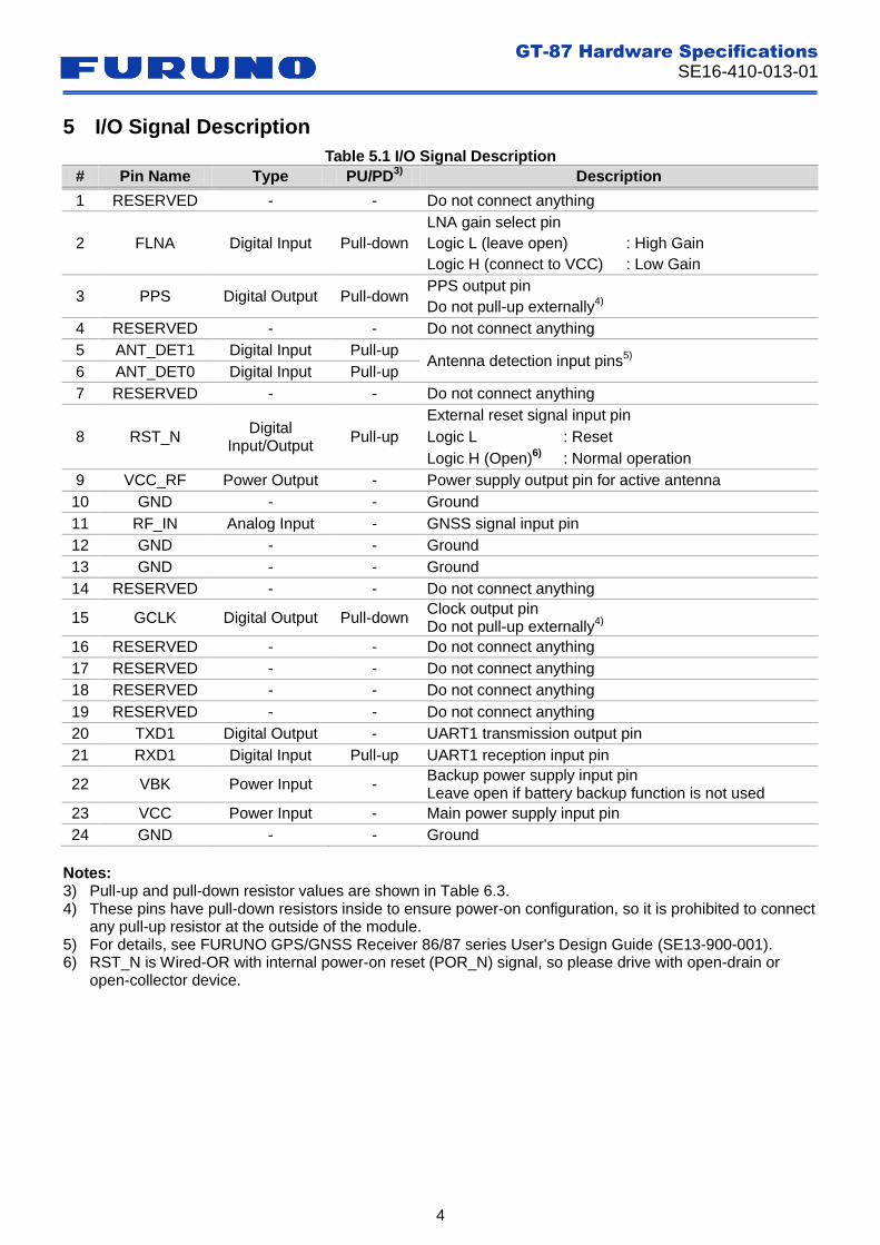
5 I/O Signal Description
Table 5.1 I/O Signal Description
# Pin Name Type PU/PD3)
Description
1 RESERVED - - Do not connect anything
2 FLNA Digital Input Pull-down
LNA gain select pin
Logic L (leave open) : High Gain
Logic H (connect to VCC) : Low Gain
3 PPS Digital Output Pull-down PPS output pin
Do not pull-up externally4)
4 RESERVED - - Do not connect anything
5 ANT_DET1 Digital Input Pull-up Antenna detection input pins
5)
6 ANT_DET0 Digital Input Pull-up
7 RESERVED - - Do not connect anything
8 RST_N Digital
Input/Output Pull-up
External reset signal input pin
Logic L : Reset
Logic H (Open)6)
: Normal operation
9 VCC_RF Power Output - Power supply output pin for active antenna
10 GND - - Ground
11 RF_IN Analog Input - GNSS signal input pin
12 GND - - Ground
13 GND - - Ground
14 RESERVED - - Do not connect anything
15 GCLK Digital Output Pull-down Clock output pin Do not pull-up externally
4)
16 RESERVED - - Do not connect anything
17 RESERVED - - Do not connect anything
18 RESERVED - - Do not connect anything
19 RESERVED - - Do not connect anything
20 TXD1 Digital Output - UART1 transmission output pin
21 RXD1 Digital Input Pull-up UART1 reception input pin
22 VBK Power Input - Backup power supply input pin Leave open if battery backup function is not used
23 VCC Power Input - Main power supply input pin
24 GND - - Ground
Notes: 3) Pull-up and pull-down resistor values are shown in Table 6.3. 4) These pins have pull-down resistors inside to ensure power-on configuration, so it is prohibited to connect
any pull-up resistor at the outside of the module. 5) For details, see FURUNO GPS/GNSS Receiver 86/87 series User's Design Guide (SE13-900-001). 6) RST_N is Wired-OR with internal power-on reset (POR_N) signal, so please drive with open-drain or
open-collector device.
GT-87 Hardware Specifications
SE16-410-013-01
5
6 Electrical Characteristics
Absolute Maximum Rating 6.1
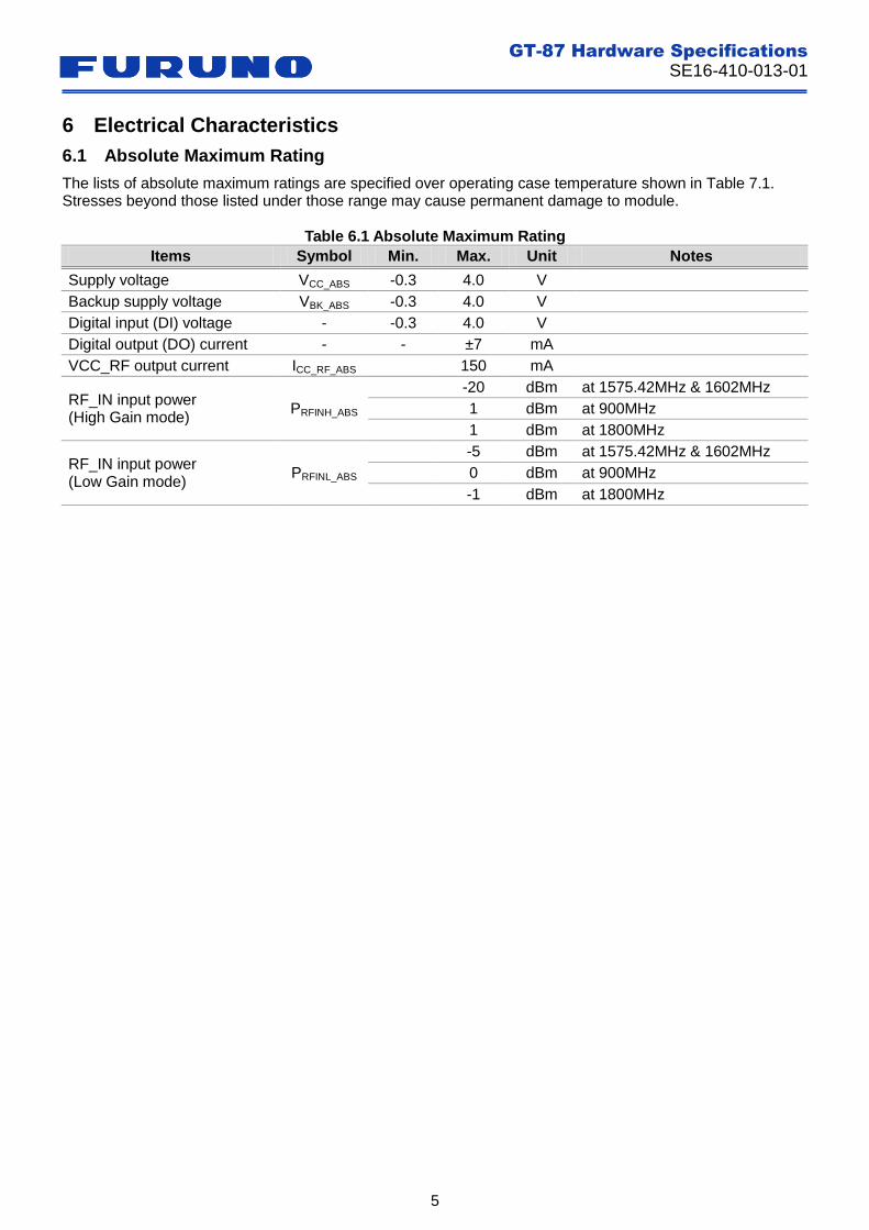
The lists of absolute maximum ratings are specified over operating case temperature shown in Table 7.1. Stresses beyond those listed under those range may cause permanent damage to module.
Table 6.1 Absolute Maximum Rating
Items Symbol Min. Max. Unit Notes
Supply voltage VCC_ABS -0.3 4.0 V
Backup supply voltage VBK_ABS -0.3 4.0 V
Digital input (DI) voltage - -0.3 4.0 V
Digital output (DO) current - - ±7 mA
VCC_RF output current ICC_RF_ABS 150 mA
RF_IN input power (High Gain mode)
PRFINH_ABS
-20 dBm at 1575.42MHz & 1602MHz
1 dBm at 900MHz
1 dBm at 1800MHz
RF_IN input power (Low Gain mode)
PRFINL_ABS
-5 dBm at 1575.42MHz & 1602MHz
0 dBm at 900MHz
-1 dBm at 1800MHz
GT-87 Hardware Specifications
SE16-410-013-01
6
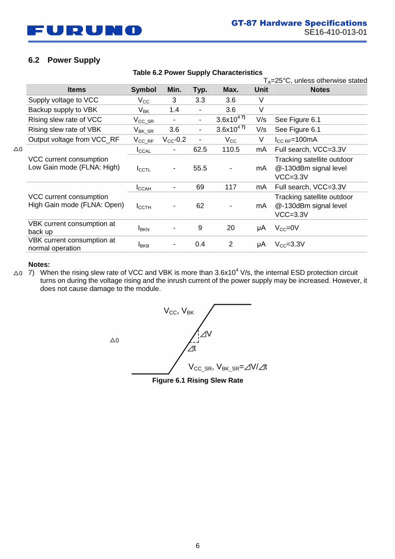
Power Supply 6.2
Table 6.2 Power Supply Characteristics TA=25°C, unless otherwise stated
Items Symbol Min. Typ. Max. Unit Notes
Supply voltage to VCC VCC 3 3.3 3.6 V
Backup supply to VBK VBK 1.4 - 3.6 V
Rising slew rate of VCC VCC_SR - - 3.6x10⁴ 7)
V/s See Figure 6.1
Rising slew rate of VBK VBK_SR 3.6 - 3.6x10⁴ 7)
V/s See Figure 6.1
Output voltage from VCC_RF VCC_RF VCC-0.2 - VCC V ICC RF=100mA
VCC current consumption Low Gain mode (FLNA: High)
ICCAL - 62.5 110.5 mA Full search, VCC=3.3V
ICCTL - 55.5 - mA
Tracking satellite outdoor
@-130dBm signal level
VCC=3.3V
VCC current consumption High Gain mode (FLNA: Open)
ICCAH - 69 117 mA Full search, VCC=3.3V
ICCTH - 62 - mA
Tracking satellite outdoor
@-130dBm signal level
VCC=3.3V
VBK current consumption at back up
IBKN - 9 20 μA VCC=0V
VBK current consumption at normal operation
IBKB - 0.4 2 μA VCC=3.3V
Notes: 7) When the rising slew rate of VCC and VBK is more than 3.6x10
4 V/s, the internal ESD protection circuit
turns on during the voltage rising and the inrush current of the power supply may be increased. However, it does not cause damage to the module.
VCC_SR, VBK_SR=⊿V/⊿t
VCC, VBK
⊿V
⊿t
Figure 6.1 Rising Slew Rate
△0
△0
△0
GT-87 Hardware Specifications
SE16-410-013-01
7
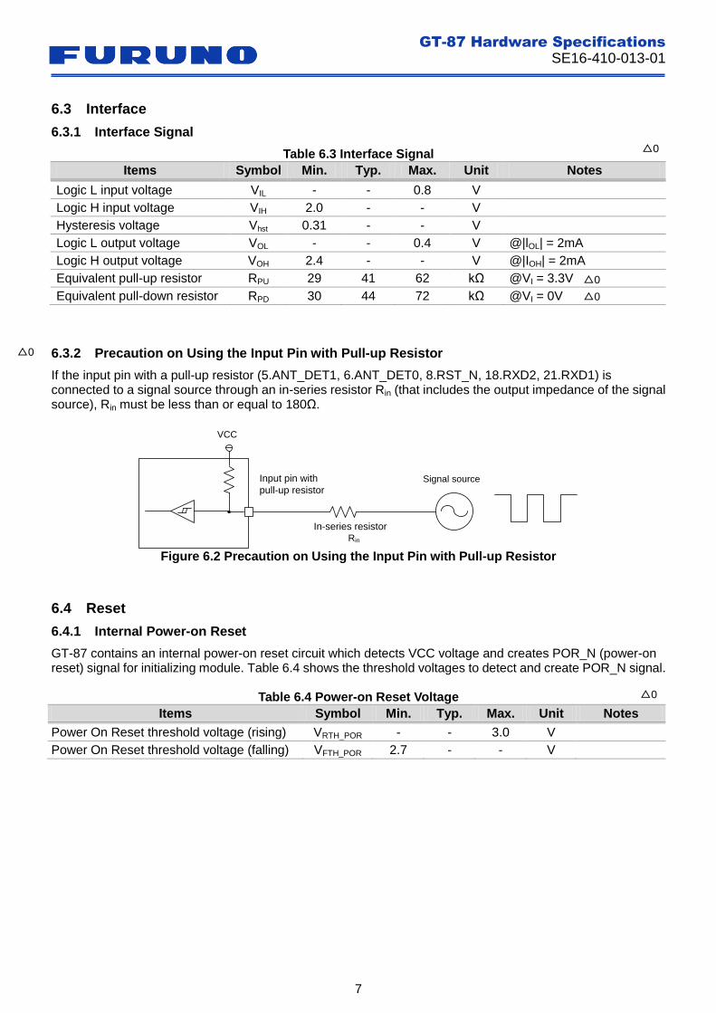
Interface 6.3
6.3.1 Interface Signal
Table 6.3 Interface Signal
Items Symbol Min. Typ. Max. Unit Notes
Logic L input voltage VIL - - 0.8 V
Logic H input voltage VIH 2.0 - - V
Hysteresis voltage Vhst 0.31 - - V
Logic L output voltage VOL - - 0.4 V @|lOL| = 2mA
Logic H output voltage VOH 2.4 - - V @|IOH| = 2mA
Equivalent pull-up resistor RPU 29 41 62 kΩ @VI = 3.3V
Equivalent pull-down resistor RPD 30 44 72 kΩ @VI = 0V
6.3.2 Precaution on Using the Input Pin with Pull-up Resistor
If the input pin with a pull-up resistor (5.ANT_DET1, 6.ANT_DET0, 8.RST_N, 18.RXD2, 21.RXD1) is connected to a signal source through an in-series resistor Rin (that includes the output impedance of the signal source), Rin must be less than or equal to 180Ω.
Input pin with
pull-up resistorSignal source
VCC
In-series resistorRin
Figure 6.2 Precaution on Using the Input Pin with Pull-up Resistor
Reset 6.4
6.4.1 Internal Power-on Reset
GT-87 contains an internal power-on reset circuit which detects VCC voltage and creates POR_N (power-on reset) signal for initializing module. Table 6.4 shows the threshold voltages to detect and create POR_N signal.
Table 6.4 Power-on Reset Voltage
Items Symbol Min. Typ. Max. Unit Notes Power On Reset threshold voltage (rising) VRTH_POR - - 3.0 V
Power On Reset threshold voltage (falling) VFTH_POR 2.7 - - V
△0
△0
△0
△0
△0
GT-87 Hardware Specifications
SE16-410-013-01
8
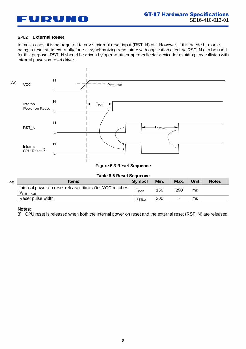
6.4.2 External Reset
In most cases, it is not required to drive external reset input (RST_N) pin. However, if it is needed to force being in reset state externally for e.g. synchronizing reset state with application circuitry, RST_N can be used for this purpose. RST_N should be driven by open-drain or open-collector device for avoiding any collision with internal power-on reset driver.
VCCH
L
VRTH_POR
Internal
Power on Reset
H
L
TPOR
RST_N
H
L
TRSTLW
Internal
CPU Reset
H
L
Figure 6.3 Reset Sequence
Table 6.5 Reset Sequence
Items Symbol Min. Max. Unit Notes
Internal power on reset released time after VCC reaches VRTH_POR
TPOR 150 250 ms
Reset pulse width TRSTLW 300 - ms
Notes: 8) CPU reset is released when both the internal power on reset and the external reset (RST_N) are released.
8)
△0
△0
GT-87 Hardware Specifications
SE16-410-013-01
9
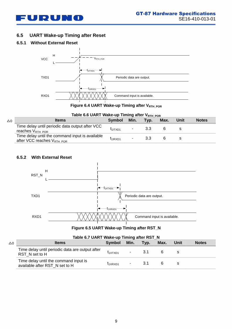
UART Wake-up Timing after Reset 6.5
6.5.1 Without External Reset
VCC
TXD1
RXD1
H
L
Periodic data are output.
t1ITXD1
t1IRXD1
Command input is available.
VRTH_POR
Figure 6.4 UART Wake-up Timing after VRTH_POR
Table 6.6 UART Wake-up Timing after VRTH_POR
Items Symbol Min. Typ. Max. Unit Notes
Time delay until periodic data output after VCC reaches VRTH_POR
t1ITXD1 - 3.3 6 s
Time delay until the command input is available after VCC reaches VRTH_POR
t1IRXD1 - 3.3 6 s
6.5.2 With External Reset
RST_N
TXD1
RXD1
H
L
Periodic data are output.
t1XTXD1
t1XRXD1
Command input is available.
Figure 6.5 UART Wake-up Timing after RST_N
Table 6.7 UART Wake-up Timing after RST_N
Items Symbol Min. Typ. Max. Unit Notes
Time delay until periodic data are output after RST_N set to H
t1XTXD1 - 3.1 6 s
Time delay until the command input is available after RST_N set to H
t1XRXD1 - 3.1 6 s
△0
△0
GT-87 Hardware Specifications
SE16-410-013-01
10
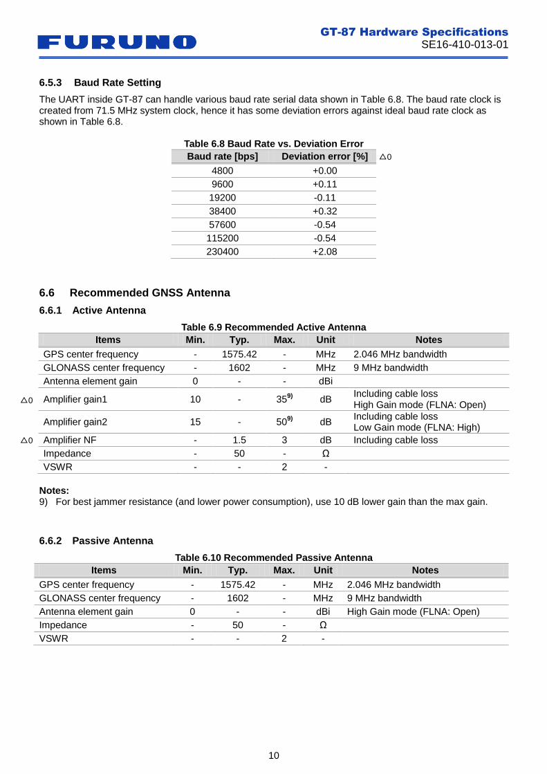
6.5.3 Baud Rate Setting
The UART inside GT-87 can handle various baud rate serial data shown in Table 6.8. The baud rate clock is created from 71.5 MHz system clock, hence it has some deviation errors against ideal baud rate clock as shown in Table 6.8.
Table 6.8 Baud Rate vs. Deviation Error
Baud rate [bps] Deviation error [%]
4800 +0.00
9600 +0.11
19200 -0.11
38400 +0.32
57600 -0.54
115200 -0.54
230400 +2.08
Recommended GNSS Antenna 6.6
6.6.1 Active Antenna
Table 6.9 Recommended Active Antenna
Items Min. Typ. Max. Unit Notes
GPS center frequency - 1575.42 - MHz 2.046 MHz bandwidth
GLONASS center frequency - 1602 - MHz 9 MHz bandwidth
Antenna element gain 0 - - dBi
Amplifier gain1 10 - 359)
dB Including cable loss High Gain mode (FLNA: Open)
Amplifier gain2 15 - 509)
dB Including cable loss Low Gain mode (FLNA: High)
Amplifier NF - 1.5 3 dB Including cable loss
Impedance - 50 - Ω
VSWR - - 2 -
Notes: 9) For best jammer resistance (and lower power consumption), use 10 dB lower gain than the max gain.
6.6.2 Passive Antenna
Table 6.10 Recommended Passive Antenna
Items Min. Typ. Max. Unit Notes
GPS center frequency - 1575.42 - MHz 2.046 MHz bandwidth
GLONASS center frequency - 1602 - MHz 9 MHz bandwidth
Antenna element gain 0 - - dBi High Gain mode (FLNA: Open)
Impedance - 50 - Ω
VSWR - - 2 -
△0
△0
△0
GT-87 Hardware Specifications
SE16-410-013-01
11
7 Environmental Specifications
Table 7.1 Environmental Specifications
Items Specification Unit Notes
Operating temperature -40 to +85 °C
Storage temperature -40 to +85 °C
Operation humidity 85(MAX) %R.H TA= 60°C, No condensation
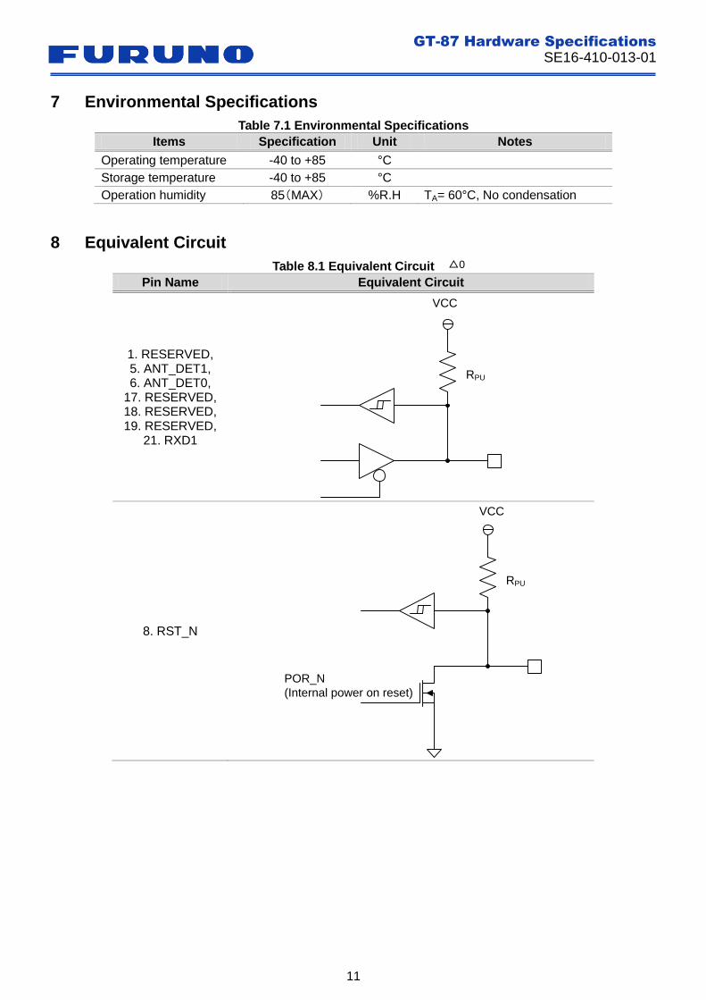
8 Equivalent Circuit
Table 8.1 Equivalent Circuit
Pin Name Equivalent Circuit
1. RESERVED, 5. ANT_DET1, 6. ANT_DET0,
17. RESERVED, 18. RESERVED, 19. RESERVED,
21. RXD1
8. RST_N
VCC
POR_N
(Internal power on reset)
RPU
VCC
RPU
△0
GT-87 Hardware Specifications
SE16-410-013-01
12
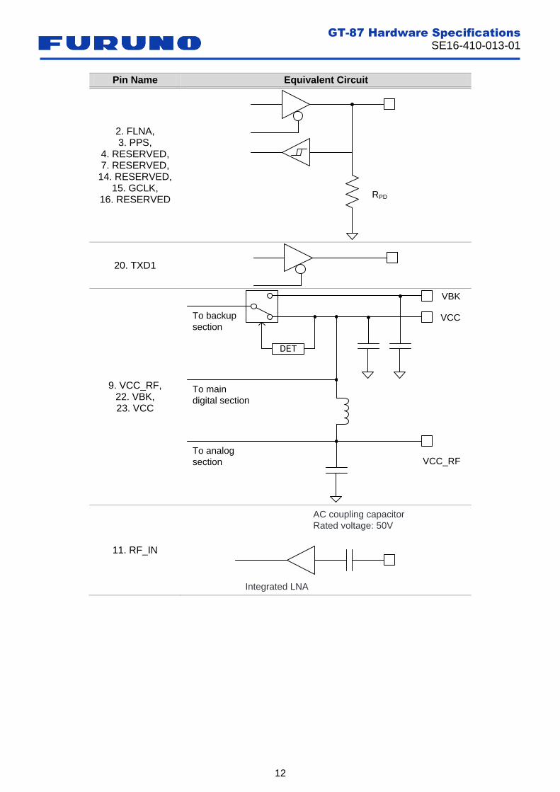
Pin Name Equivalent Circuit
2. FLNA, 3. PPS,
4. RESERVED, 7. RESERVED,
14. RESERVED, 15. GCLK,
16. RESERVED RPD
20. TXD1
9. VCC_RF, 22. VBK, 23. VCC
VCC
VBK
DET
To main
digital section
To backup
section
To analog
section VCC_RF
11. RF_IN
Integrated LNA
AC coupling capacitor
Rated voltage: 50V
GT-87 Hardware Specifications
SE16-410-013-01
13
9 Mechanical Specifications
Package Dimension 9.1
A
BC
G DE F E
K
N
M
1 pin
H
SEATING PLANEY
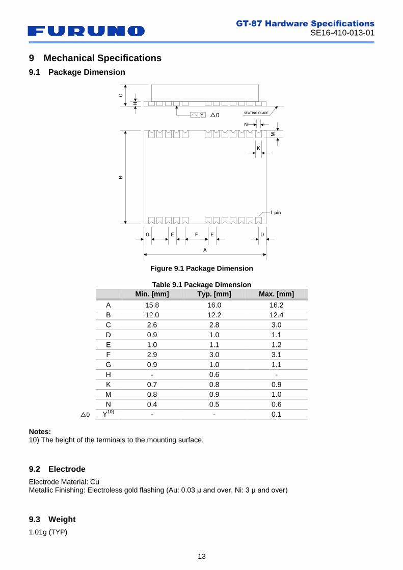
Figure 9.1 Package Dimension
Table 9.1 Package Dimension
Min. [mm] Typ. [mm] Max. [mm]
A 15.8 16.0 16.2
B 12.0 12.2 12.4
C 2.6 2.8 3.0
D 0.9 1.0 1.1
E 1.0 1.1 1.2
F 2.9 3.0 3.1
G 0.9 1.0 1.1
H - 0.6 -
K 0.7 0.8 0.9
M 0.8 0.9 1.0
N 0.4 0.5 0.6
Y10)
- - 0.1
Notes: 10) The height of the terminals to the mounting surface.
Electrode 9.2
Electrode Material: Cu Metallic Finishing: Electroless gold flashing (Au: 0.03 μ and over, Ni: 3 μ and over)
Weight 9.3
1.01g (TYP)
△0
△0
GT-87 Hardware Specifications
SE16-410-013-01
14
Pin Position List 9.4
14:RESERVED
13: GND
8: RST_N
9: VCC_RF
1: RESERVED
12: GND
10: GND15: GCLK
16:RESERVED
5: ANT_DET1
6: ANT_DET0
4: RESERVED
24: GND
3: PPS
2: FLNA
17: RESERVED
11: RF_IN
19: RESERVED
20: TXD1
21: RXD1
22: VBK
23: VCC
18: RESERVED 7: RESERVED
TOP VIEW
Figure 9.2 Pin Position List
10 Reference Design
Recommended Land Pattern 10.1
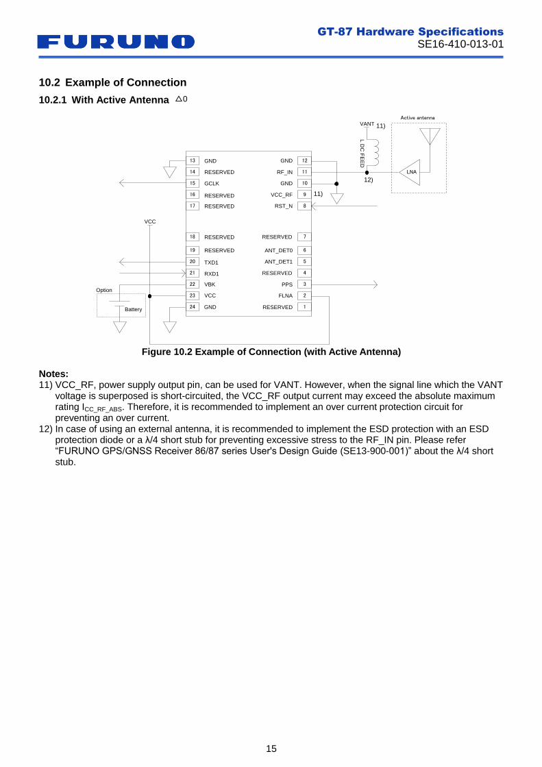
There are some signal lines and via holes on the bottom of the module. For avoiding any signal shortage, do not put any signal line nor via hole at the part of the user’s board where is facing to the bottom of the module.
12.2
16
.0
1.0
1.1
3.0
0.8
0.9 0.8
Unit: [mm]
1 pin
Pattern
Prohibition Area
Figure 10.1 Recommended Land Pattern
△0
GT-87 Hardware Specifications
SE16-410-013-01
15
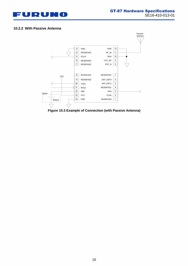
Example of Connection 10.2
10.2.1 With Active Antenna
VCC
Active antenna
Battery
LNA
Option
RESERVED
GND
RST_N
VCC_RF
RESERVED
GND
GNDGCLK
RESERVED
ANT_DET1
ANT_DET0
RESERVED
GND
PPS
FLNA
RESERVED
RF_IN
RESERVED
TXD1
RXD1
VBK
VCC
RESERVED RESERVED
13
22
14
21
24
16
23
15
17
20
19
18
12
3
11
4
1
9
2
10
8
5
6
7
L D
C F
EE
D
VANT
Figure 10.2 Example of Connection (with Active Antenna)
Notes: 11) VCC_RF, power supply output pin, can be used for VANT. However, when the signal line which the VANT
voltage is superposed is short-circuited, the VCC_RF output current may exceed the absolute maximum rating ICC_RF_ABS. Therefore, it is recommended to implement an over current protection circuit for preventing an over current.
12) In case of using an external antenna, it is recommended to implement the ESD protection with an ESD protection diode or a λ/4 short stub for preventing excessive stress to the RF_IN pin. Please refer “FURUNO GPS/GNSS Receiver 86/87 series User's Design Guide (SE13-900-001)” about the λ/4 short stub.
△0
11)
12)
11)
GT-87 Hardware Specifications
SE16-410-013-01
16
10.2.2 With Passive Antenna
VCC
Passive
antenna
Battery
Option
13
22
14
21
24
16
23
15
17
20
19
18
12
3
11
4
1
9
2
10
8
5
6
7
RESERVED
GND
RST_N
VCC_RF
RESERVED
GND
GNDGCLK
RESERVED
ANT_DET1
ANT_DET0
RESERVED
GND
PPS
FLNA
RESERVED
RF_IN
RESERVED
TXD1
RXD1
VBK
VCC
RESERVED RESERVED
Figure 10.3 Example of Connection (with Passive Antenna)
GT-87 Hardware Specifications
SE16-410-013-01
17
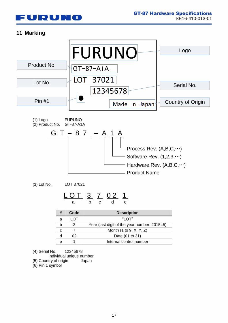
11 Marking
Product No.
Country of Origin
Serial No.Lot No.
Logo
Pin #1
GT-87-A1A
(1) Logo FURUNO (2) Product No. GT-87-A1A
G T – 8 7 – A 1 A
Product Name
Hardware Rev. (A,B,C,…)
Software Rev. (1,2,3,…)
Process Rev. (A,B,C,…)
(3) Lot No. LOT 37021
L O T 3 7 0 2 1 a b c d e
# Code Description
a LOT “LOT”
b 3 Year (last digit of the year number: 2015=5)
c 7 Month (1 to 9, X, Y, Z)
d 02 Date (01 to 31)
e 1 Internal control number
(4) Serial No. 12345678 Individual unique number (5) Country of origin Japan (6) Pin 1 symbol
GT-87 Hardware Specifications
SE16-410-013-01
18
12 Handling Precaution
The section especially describes the conditions and the requests when mounting the product. Surface mount products like this may have a crack when thermal stress is applied during surface mount assembly after they absorb atmospheric moisture. Therefore, please observe the following precautions: (1) This product contains semi-conductor inside. While handling this, be careful about the static electrical
charge. To avoid it, use conductive mat, ground wristband, anti-static shoes, ionizer, etc. as may be necessary.
(2) Try to avoid mechanical shock and vibration. Try not to drop this product. (3) When mounting this product, be aware of the location of the electrode. (4) This product should not be washed. (5) The reflow conditions are as shown in Section 13.1. The reflow can be done twice at most. (6) Surface mount products like this may have a crack when thermal stress is applied during surface mount
assembly after they absorb atmospheric moisture. Therefore, please observe the following precautions:
① This moisture barrier bag may be stored unopened 12 months at or below 30°C/90%RH.
② After opening the moisture bag, the packages should be assembled within 1 week in the environment less than 30°C/60%RH.
③ If, upon opening, the moisture indicator card in the bag shows humidity above 30% or the expiration date has passed, they may still be used with the addition of a bake of 24 hours at 125°C.
Caution: If the packing material is likely to melt at 125°C, heat-proof tray or aluminum magazine etc. must be used for high temperature.
④ Expiration date: 12 months from the sealing date. (7) This module includes a crystal oscillator. It may not be able to maintain the characteristic under the
vibrating condition, windy and cold conditions and noisy conditions. Please evaluate the module on ahead, if it may be used under these conditions.
GT-87 Hardware Specifications
SE16-410-013-01
19
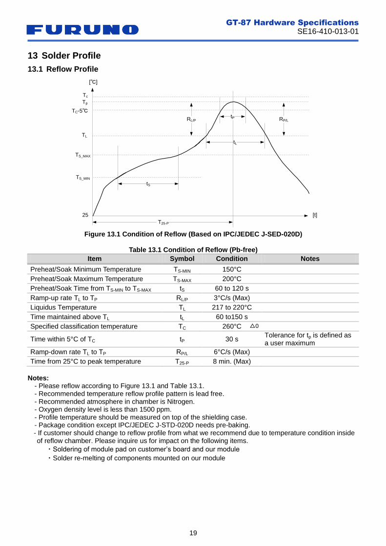
13 Solder Profile
Reflow Profile 13.1
Figure 13.1 Condition of Reflow (Based on IPC/JEDEC J-SED-020D)
Table 13.1 Condition of Reflow (Pb-free)
Item Symbol Condition Notes
Preheat/Soak Minimum Temperature TS-MIN 150°C
Preheat/Soak Maximum Temperature TS-MAX 200°C
Preheat/Soak Time from TS-MIN to TS-MAX tS 60 to 120 s
Ramp-up rate TL to TP RL/P 3°C/s (Max)
Liquidus Temperature TL 217 to 220°C
Time maintained above TL tL 60 to150 s
Specified classification temperature TC 260°C
Time within 5°C of TC tP 30 s Tolerance for tp is defined as a user maximum
Ramp-down rate TL to TP RP/L 6°C/s (Max)
Time from 25°C to peak temperature T25-P 8 min. (Max)
Notes:
- Please reflow according to Figure 13.1 and Table 13.1. - Recommended temperature reflow profile pattern is lead free. - Recommended atmosphere in chamber is Nitrogen. - Oxygen density level is less than 1500 ppm. - Profile temperature should be measured on top of the shielding case. - Package condition except IPC/JEDEC J-STD-020D needs pre-baking. - If customer should change to reflow profile from what we recommend due to temperature condition inside of reflow chamber. Please inquire us for impact on the following items.
・Soldering of module pad on customer’s board and our module
・Solder re-melting of components mounted on our module
25
[℃]
Tc
TS_MIN
TS_MAX
[t]
T25-P
tL
tP
TC-5℃
RL/P
TL
RP/L
tS
Tp
△0
GT-87 Hardware Specifications
SE16-410-013-01
20
Table 13.2 shows the moisture sensitivity level and number of reflow for assembly at user side.
Table 13.2 Moisture Sensitivity Level, Number of Reflow for Assembly at User Side
Item Condition
Moisture Sensitivity Level 3
Number of reflow for assembly at user side 2
Precaution about Partial Heating with the Way except Reflow 13.2
If the internal temperature when the product is heated partially with, for example, like a soldering iron, hot air and light beam welder exceeds 215 degree, the internal wiring may be disconnected by thermal stress.
14 Special Instruction
Electronic Component 14.1
Components in GT-87 module such as chip resistors, capacitors, memories and TCXO are planned to be purchased from multiple manufacturers/vendors according to FURUNO’s procurement policy. So it is possible that multiple components from multiple manufacturers/vendors could be used even in the same production lot.
ESD Damage 14.2
GT-87 module may be damaged by ESD. FURUNO recommends that all modules should be handled with appropriate precautions. Failure to observe proper handling and installation procedures may cause damage.
RoHS 14.3
GT-87 complies with RoHS directives.
15 Reference Documents
- FURUNO 86&87Module Package Specifications (Document No. SE13-600-024) - FURUNO 86/87 module products series reliability test (Document No. SE13-600-002) - FURUNO GPS/GNSS Receiver 86/87 series User’s Design Guide. (Document No. SE13-900-001)