Embed Size (px)
Citation preview
FUNDAMENTALS OF SOLIDSTATE ENGINEERING
FUNDAMENTALS OF SOLIDSTATE ENGINEERING
by
Manijeh RazeghiNorthwestern University, U.S.A.
KLUWER ACADEMIC PUBLISHERS NEW YORK, BOSTON, DORDRECHT, LONDON, MOSCOW

eBook ISBN: 0-306-47567-7Print ISBN: 0-7923-7629-3
©2002 Kluwer Academic PublishersNew York, Boston, Dordrecht, London, Moscow
Print ©2002 Kluwer Academic Publishers
All rights reserved
No part of this eBook may be reproduced or transmitted in any form or by any means, electronic,mechanical, recording, or otherwise, without written consent from the Publisher
Created in the United States of America
Visit Kluwer Online at: http://kluweronline.comand Kluwer's eBookstore at: http://ebooks.kluweronline.com
Dordrecht

Contents
List of Symbols xv
xixForeword
Preface xxi
1258
1. Crystalline Properties of Solids1.1.1.2.1.3.1.4.1.5.
Crystal lattices and the seven crystal systemsIntroduction
The unit cell concept111313141516171818192021212123232828303131323435
1.8.1.1.8.2.1.8.3.1.8.4.1.8.5.1.8.6.1.8.7.
1.6.1.7.1.8.
1.5.1.1.5.2.1.5.3.1.5.4.1.5.5.1.5.6.1.5.7.1.5.8.1.5.9.1.5.10.1.5.11.1.5.12.
Bravais latticesPoint groups
group (plane reflection)groups (rotation)and groups
groupsand groups
groupand groups
T groupgroup
O groupgroup
List of crystallographic point groupsSpace groupsDirections and planes in crystals: Miller indicesReal crystal structures
Diamond structureZinc blende structureSodium chloride structureCesium chloride structureHexagonal close-packed structureWurtzite structurePacking factor
Fundamentals of Solid State Engineeringvi
2.
373739
4141
4248505454565860616164666768
7171727477777979
2.1.2.2.
2.3.2.4.2.5.
2.5.1.2.5.2.2.5.3.2.5.4.2.5.5.2.5.6.
2.6.2.7.
3.1.3.1.1.3.1.2.3.1.3.3.1.4.
3.2.3.2.1.3.2.2.
3.3.1.3.3.2.3.3.3.
3.4.3.5.
4.1.4.2.
4.
3.3.
100
1.9. SummaryFurther readingProblems
Electronic Structure of AtomsIntroductionSpectroscopic emission lines and atomic structure of
hydrogenAtomic orbitalsStructures of atoms with many electronsBonds in solids
General principlesIonic bondsCovalent bondsMixed bondsMetallic bondsSecondary bonds
Introduction to energy bandsSummary
Further readingProblems
3. Introduction to Quantum MechanicsThe quantum concepts
Blackbody radiationThe photoelectric effectWave-particle dualityThe Davisson-Germer experiment
Elements of quantum mechanicsBasic formalismGeneral properties of wavefunctions and the Schrödinger
828282848793969697
9999
equationSimple quantum mechanical systems
Free particleParticle in a 1-D boxParticle in a finite potential well
Reciprocal latticeSummary
Further readingProblems
Electrons and Energy Band Structures in CrystalsIntroductionElectrons in a crystal

Contents vii
100102106109111113115118119122124125127128130132133133134
135135136136141143143148152152155157157158161163167167168168169
171171
6.
5.
4.2.1.4.2.2.4.2.3.4.2.4.4.2.5.4.2.6.4.2.7.4.2.8.4.2.9.4.2.10.
4.3.1.4.3.2.4.3.3.
4.4.4.5.
5.1.5.2.
5.2.1.5.2.2.
5.3.5.3.1.5.3.2.5.3.3.
5.4.5.5.5.6.
5.6.1.5.6.2.
5.7.5.7.1.5.7.2.
5.8.
Bloch theoremOne-dimensional Kronig-Penney modelEnergy bandsNearly-free electron approximationTight binding approximationHeisenberg uncertainty principleDynamics of electrons in a crystalFermi energyElectron distribution functionElectrons and holes
4.3. Band structures in real semiconductorsFirst Brillouin zone of an fcc latticeFirst Brillouin zone of a bcc latticeFirst Brillouin zones of a few semiconductors
Band structures in metalsSummary
ReferencesFurther readingProblems
Low Dimensional Quantum StructuresIntroductionDensity of states (3D)
Direct calculationOther approach
Two-dimensional structures: quantum wellsEnergy spectrumDensity of statesEffect of effective mass
One-dimensional structures: quantum wiresZero-dimensional structures: quantum dotsOptical properties of 3D and 2D structures
Absorption coefficientExcitonic effects
Examples of low dimensional structuresQuantum wiresQuantum dots
SummaryReferencesFurther readingProblems
Phonons6.1. Introduction
viii Fundamentals of Solid State Engineering
171174174176177179182182183189191193194195
197197197197200203
8.1.8.2.8.3.8.4.8.5.8.6.8.7.8.8.8.9.8.10.
8.
7.4.7.5.7.6.
6.2.6.3.
6.3.1.6.3.2.6.3.3.
6.4.6.5.
6.5.1.6.5.2.6.5.3.
6.6.6.7.
7.7.1.7.2.
7.2.1.7.2.2.
7.3.7.3.1.
7.3.2.
Interaction of atoms in crystals: origin and formalismOne-dimensional monoatomic harmonic crystal
Traveling wave formalism
ReferencesFurther readingProblems
Boundary conditionsPhonon dispersion relation
Sound velocityOne-dimensional diatomic harmonic crystal
FormalismPhonon dispersion relation
PhononsSummary
Extension to three-dimensional case
Further readingProblems
Thermal Properties of CrystalsIntroductionPhonon density of states (Debye model)
Debye modelPhonon density of states
Heat capacityLattice contribution to the heat capacity (Debye model)
203210213215219219219220
221221222225228231233237238242246246247
Equilibrium Charge Carrier Statistics in Semiconductors
Electronic contribution to the heat capacityThermal expansionThermal conductivitySummary
IntroductionDensity of statesEffective density of states (conduction band)Effective density of states (valence band)Mass action lawDoping: intrinsic vs. extrinsic semiconductorCharge neutralityFermi energy as a function of temperatureCarrier concentration in a semiconductor
SummaryFurther readingProblems
Contents
9.
ix
249249250250255256257259261261262263265270272273273278287290291291293
297297298298299304306309311313314317319323
331333334337338
9.1.9.2.
9.2.1.9.2.2.
9.3.9.3.1.9.3.2.9.3.3.
9.4.9.4.1.9.4.2.9.4.3.
9.5.9.6.
9.6.1.9.6.2.9.6.3.9.6.4.9.6.5.
9.7.
Non-Equilibrium Electrical Properties of SemiconductorsIntroductionElectrical conductivity
Ohm’s law in solidsCase of semiconductors
Hall effectP-type semiconductorN-type semiconductor
10.2.1.10.2.2.10.2.3.10.2.4.10.2.5.10.2.6.
10.3.1.10.3.2.10.3.3.10.3.4.10.3.5.
10.4.1.10.4.2.
10.5.
10.4.Avalanche breakdownZener breakdown
Metal-semiconductor junctions
Deviations from the ideal p-n diode case
Minority and majority carrier currents in neutral regionsIdeal p-n junction diode equationA quantitative descriptionReverse bias: a qualitative descriptionForward bias: a qualitative description
10.3. Non-equilibrium properties of p-n junctionsEnergy band profile and Fermi energyDepletion widthBuilt-in potentialBuilt-in electric fieldDepletion approximationIdeal p-n junction
10.1.10.2.
IntroductionIdeal p-n junction at equilibrium
Semiconductor Junctions10.
ProblemsFurther reading
SummarySurface recombinationAuger band-to-band recombinationSchokley-Read-Hall recombinationDirect band-to-band recombinationCarrier generation
Carrier generation and recombination mechanismsQuasi-Fermi energy
Diffusion lengthsEinstein relationsDiffusion currents
Compensated semiconductorCharge carrier diffusion
x
10.5.1.10.5.2.
10.6.
11.1.11.2.
11.2.1.11.2.2.11.2.3.
11.3.1.11.3.2.11.3.3.11.3.4.
11.4.11.4.1.11.4.2.11.4.3.11.4.4.11.4.5.
11.5.
12.2.1.12.2.2.12.2.3.12.2.4.
12.3.1.12.3.2.12.3.3.12.3.4.
12.4.1.12.4.2.12.4.3.
338340344344346
349349350350352353357357361362365366366367371378383384384385386
387387388388390395397400401403404405408408409410
12.4.
12.3.
Ion range distributionParameters of ion implantationIon generation
Ion implantation of dopantsJunction formationLimited-source diffusion: drive-inConstant-source diffusion: predepositionDiffusion process
Diffusion of dopantsOxide thickness characterizationFactors influencing oxidation rateModeling of oxidationOxidation process
Oxidation12.2.12.1. IntroductionSemiconductor Device Technology
ProblemsFurther readingReferences
SummaryEx-situ characterization of epitaxial thin filmsMolecular beam epitaxyMetalorganic chemical vapor depositionVapor phase epitaxyLiquid phase epitaxy
Epitaxial growth techniquesCrystal wafer fabricationFloat-zone crystal growth methodBridgman growth methodCzochralski growth method
11.3. Bulk single crystal growth techniquesIII-V quaternary compoundsIII-V ternary compoundsIII-V binary compounds
III-V semiconductor alloysIntroduction
Compound Semiconductors and Crystal Growth Techniques
ProblemsFurther reading
SummarySchottky and ohmic contactsFormalism
Fundamentals of Solid State Engineering
12.
11.

Contents
13.
411412414416416417418
419419420421423427428430431433434437438440440442446447447449449450453454454456458459460460461
463463464466
xi
14.14.1.14.2.14.3.
13.5.1.13.5.2.13.5.3.
13.4.1.13.4.2.13.4.3.13.4.4.13.4.5.
13.3.1.13.3.2.13.3.3.13.3.4.13.3.5.
13.2.1.13.2.2.13.2.3.13.2.4.
13.1.13.2.
12.5.1.12.5.2.
12.6.
12.5.
13.6.1.13.6.2.13.6.3.
13.7.
13.6.
13.4. Etching
13.3.
Bipolar junction transistorsOverview of amplification and switchingIntroduction
Transistors
ProblemsFurther readingReferences
SummaryPackagingWire bondingDicing
Packaging of devicesSputtering depositionVacuum evaporationMetal interconnections
Metallization13.5.Ion millingSputter etchingReactive ion etchingPlasma etchingWet chemical etching
Examples of structuresMultilayer resist systemsParameters of electron-beam lithographyElectron-beam lithography processElectron-beam lithography system
Electron-beam lithographyDirect patterning and lift-off techniquesExposure and developingPositive and negative resistsMask fabrication
PhotolithographyIntroduction
Semiconductor Device Processing
ProblemsFurther readingReferences
SummaryJunction depthSheet resistivity
Characterization of diffused and implanted layers

Principles of operation for bipolar junction transistors466467471474475476478481482483485485487
489489490491492494496504507507511512513517517520524527528529530533536538540540542543
14.3.2.14.3.3.14.3.4.
14.4.1.14.4.2.
14.5.1.14.5.2.
15.3.1.15.3.2.15.3.3.15.3.4.15.3.5.
15.5.1.15.5.2.15.5.3.15.5.4.15.5.5.15.5.6.15.5.7.15.5.8.15.5.9.15.5.10.15.5.11.15.5.12.15.5.13.
15.6.
Problems
15.
14.5.
14.4.
xii Fundamentals of Solid State Engineering
Further readingReferences
SummaryLow dimensional lasersVertical cavity surface emitting lasersType II lasersQuantum cascade lasers
Material choices for common interband lasersDistributed feedback lasersLaser packagingSeparate confinement and quantum well lasersDevice FabricationHeterojunction lasersHomojunction LaserThreshold condition and output powerPopulation inversion
Semiconductor lasers15.5.15.4. Ruby laser
Waveguide design considerationsLaser propagation and beam divergenceWaveguidesResonant cavityStimulated emission
General laser theory
15.1.15.2.15.3.
Semiconductor LasersIntroductionTypes of lasers
ProblemsReferences14.6. Summary
Current-voltage characteristicsGate control
Field effect transistorsGaInP/GaAs HBTAlGaAs/GaAs HBT
Heterojunction bipolar transistorsCurrent transfer ratioElectrical charge distribution and transport in BJTsAmplification process using BJTs
14.3.1.
.
545545548549549550552555556557560561564567568568570572573574576577578578578580
583
625
xiiiContents
16.16.1.16.2.16.3.
16.3.1.16.3.2.16.3.3.16.3.4.16.3.5.
16.5.1.16.5.2.16.5.3.
16.6.1.16.6.2.16.6.3.16.6.4.16.6.5.16.6.6.16.6.7.
16.4.16.5.
16.6.
16.7.
Appendix
Index
ProblemsFurther readingReferences
SummaryPhotoelectromagnetic detectorsQuantum well intersubband photodetectorsType II superlattice photodetectorsMetal-semiconductor-metal photodiodesSchottky barrier photodiodesAvalanche photodiodesP-i-n photodiodes
Examples of photon detectorsDetectivity in photovoltaic detectorsPhotovoltaic detectorsPhotoconductive detectors
Photon detectorsThermal detectors
Frequency responseDetectivityNoise mechanismsNoise in photodetectorsResponsivity
Photodetector parametersElectromagnetic radiationIntroduction
Photodetectors

List of Symbols
AngstromBohr radiusAbsorption coefficientThermal expansion coefficient
Magnetic induction or magnetic flux densityVelocity of light in vacuumCalorieHeat capacity or specific heat, at constant volume, at constantpressureDensityDistance, thickness or diameter
Electric displacementDiffusion coefficient or diffusivity, for electrons, for holesExcess electron, hole concentration
Electric field strengthEnergyEnergy at the bottom of the conduction bandFermi energy
Quasi-Fermi energy for electrons
Quasi-Fermi energy for holes
Bandgap energyEnergy at the top of the valence bandYoung’s modulusPermittivity in vacuumPermittivityDielectric constant
ForceFrequencyFermi-Dirac distribution for electronsFermi-Dirac distribution for holesPhoton fluxSchottky potential barrier heightWork function of a metal, semiconductor
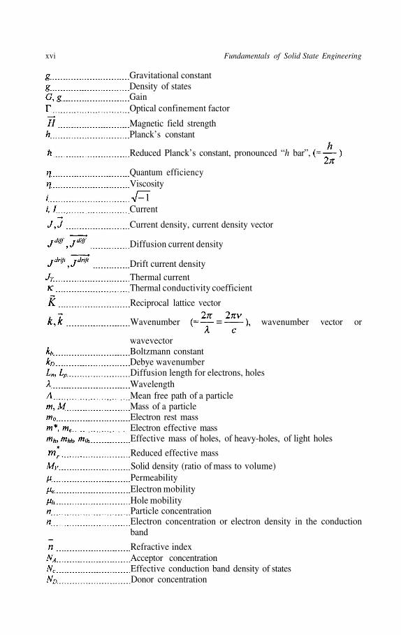
xvi Fundamentals of Solid State Engineering
Gravitational constantDensity of statesGainOptical confinement factor
Magnetic field strengthPlanck’s constant
Reduced Planck’s constant, pronounced “h bar”,
Quantum efficiencyViscosity
Current
Current density, current density vector
Diffusion current density
Drift current densityThermal currentThermal conductivity coefficient
Reciprocal lattice vector
Wavenumber wavenumber vector or
wavevectorBoltzmann constantDebye wavenumberDiffusion length for electrons, holesWavelengthMean free path of a particleMass of a particleElectron rest massElectron effective massEffective mass of holes, of heavy-holes, of light holes
Reduced effective massSolid density (ratio of mass to volume)PermeabilityElectron mobilityHole mobilityParticle concentrationElectron concentration or electron density in the conductionband
Refractive indexAcceptor concentrationEffective conduction band density of statesDonor concentration

List of Symbols xvii
Effective valence band density of statesFrequencyAvogadro numberHole concentration or hole density in the valence band
MomentumPowerWavefunctionElementary chargeElectrical resistivity
Position vector
Direct lattice vectorResistanceReflectivityRayleigh numberReynolds numberDifferential resistance at V=0 bias
Current responsivityVoltage responsivityRydberg constantElectrical conductivityCarrier lifetimePotential energyVoltage
Particle velocityGroup velocityAngular frequency
Unit vectors (cartesian coordinates)
Differential resistance at V=0 bias

Foreword
It is a pleasure to write this foreword to a book on the Fundamentals of SolidState Engineering by Professor Manijeh Razeghi.
Professor Razeghi is one of the world’s foremost experts in the field ofelectronic materials crystal growth, bandgap engineering and devicephysics. The text combines her unique expertise in the field, both as aresearcher and as a teacher. The book is all-encompassing and spansfundamental solid state physics, quantum mechanics, low dimensionalstructures, crystal growth, semiconductor device processing and technology,transistors and lasers. It is excellent material for students of solid statedevices in electrical engineering and materials science. The book haslearning aids through exceptional illustrations and end of chapter summariesand problems. Recent publications are often cited.
The text is a wonderful introduction to the field of solid stateengineering. The breadth of subjects covered serves a very usefulintegrative function in combining fundamental science with application.
I have enjoyed reading the book and am delighted Professor Razeghi hasput her lectures at Northwestern into a text for the benefit of a wideraudience.
V. NarayanamurtiJohn A. and Elizabeth S. Armstrong Professor
of Engineering and Applied Sciences and DeanHarvard University
Cambridge, Massachusetts

Preface
Solid State Engineering is a multi-disciplinary field that combinesdisciplines such as physics, chemistry, electrical engineering, materialsscience, and mechanical engineering. It provides the means to understandmatter and to design and control its properties.
The century has witnessed the phenomenal rise of Natural Scienceand Technology into all aspects of human life. Three major sciences haveemerged and marked this century, as shown in Fig. A: Physical Sciencewhich has strived to understand the structure of atoms through quantummechanics, Life Science which has attempted to understand the structure ofcells and the mechanisms of life through biology and genetics, andInformation Science which has symbiotically developed the communicativeand computational means to advance Natural Science.
Microelectronics has become one of today’s principle enablingtechnologies supporting these three major sciences and touches every aspectof human life, as illustrated in Fig. B: food, energy, transportation,

xxii Fundamentals of Solid State Engineering
communication, entertainment, health/medicine and exploration. Forexample, microelectronic devices have now become building blocks ofsystems which are used to monitor food safety and pollution, produceelectricity (solar cells) or use energy more efficiently (LED), controlelectrical vehicles (automobiles), transmit information (optical fiber andwireless communications), entertain (virtual reality, video games,computers), help cure or enhance the human body (artificial senses,optically activated medicine) and support the exploration of new realms(space, underwater).
Although impressive progress has been achieved, microelectronics isstill far from being able to imitate Nature in terms of integration density,functionality and performance. For example, a state-of-the-art low powerPentium II processor consumes nearly twice as much power as a humanbrain, while it has 1000 times fewer transistors than the number of cells in ahuman brain (Fig. C). Forecasts show that the current microelectronicstechnology is not expected to reach similar levels because of its physicallimitations.
A different approach has thus been envisioned for future advances insemiconductor science and technology in the century. This will consistof reaching closer to the structure of atoms, by employing nanoscaleelectronics. Indeed, the history of microelectronics has been, itself,characterized by a constant drive to imitate natural objects (e.g. the braincell) and thus move towards lower dimensions in order to increase

Preface xxiii
integration density, system functionality and performance (e.g. speed andpower consumption).
Thanks to nanoelectronics, it will not be unforeseeable in the near futureto create artificial atoms, molecules, and integrated multifunctionalnanoscale systems. For example, as illustrated in Fig. D below, the structureof an atom can be likened to that of a so called “quantum dot” or “Q-dot”where the three-dimensional potential well of the quantum dot replaces thenucleus of an atom. An artificial molecule can then be made from artificialatoms. Such artificial molecules will have the potential to revolutionize theperformance of optoelectronics and electronics by achieving, for example,orders of magnitude higher speed processors and denser memories. Withthese artificial atoms/molecules as building blocks, artificial activestructures such as nano-sensors, nano-machines and smart materials will bemade possible.

xxiv Fundamentals of Solid State Engineering
The scientific and technological accomplishments of earlier centuriesrepresent the first stage in the development of Natural Science andTechnology, that of understanding (Fig. E). As the century begins, weare entering the creation stage where promising opportunities lie ahead forcreative minds to enhance the quality of human life through theadvancement of science and technology.
Hopefully, by giving a rapid insight into the past and opening the doorsto the future of Solid State Engineering, this course will be able to providesome of the basis necessary for this endeavor, inspire the creativity of thereader and lead them to further explorative study.
Since 1992 when I joined Northwestern University as a faculty memberand started to teach, I have established the Solid State Engineering (SSE)research group in the Electrical and Computer Engineering Department andsubsequently created a series of related undergraduate and graduate courses.In the creative process for these courses, I studied similar programs in many
Preface xxv
other institutions such as for example Stanford University, theMassachusetts Institute of Technology, the University of Illinois at Urbana-Champaign, the California Institue of Technology, and the University ofMichigan. I reviewed numerous textbooks and reference texts in order to puttogether the teaching material students needed to learn nanotechnology,semiconductor science and technology from the basics up to modernapplications. But I soon found it difficult to find a textbook which combinedall the necessary metarial in the same volume, and this prompted me to writethis book, entitled Fundamentals of Solid State Engineering.
This book is primarily aimed at the undergraduate level but graduatestudents and researchers in the field will also find useful material in theappendix and references. After studying it, the student will be well versed ina variety of fundamental scientific concepts essential to Solid StateEngineering, as well as the latest technological advances and modernapplications in this area, and will be well prepared to meet more advancedcourses in this field.
This book is structured in two major parts. It first addresses the basicphysics concepts which are at the base of solid state matter in general andsemiconductors in particular. This includes offering an understanding of thestructure of matter, atoms and electrons (Chapters 1 and 2), followed by anintroduction to basic concepts in quantum mechanics (Chapter 3), themodeling of electrons and energy band structures in crystals (Chapter 4),and a discussion on low dimensional quantum structures including quantumwells and superlattices, wires and dots (Chapter 5). A few crystal propertieswill then be described in detail, by introducing the concept of phonons todescribe vibrations of atoms in crystals (Chapter 6) and by interpreting thethermal properties of crystals (Chapter 7). The equilibrium and non-equilibrium electrical properties of semiconductors will then be reviewed,by developing the statistics (Chapter 8) as well as the transport, generationand recombination properties of these charge carriers in semiconductors(Chapter 9). These concepts will allow then to model semiconductorjunctions (Chapter 10) which constitute the building blocks of modernelectronics. In these Chapters, the derivation of the mathematical relationshas been spelled out in thorough detail so that the reader can understand thelimits of applicability of these expressions and adapt them to his or herparticular situations.
The second part of this book reviews the technology for modern SolidState Engineering. This includes a review of compound semiconductor bulkand epitaxial thin film growth techniques (Chapter 11), followed by adescription of current semiconductor device processing and nano-fabricationtechnologies (Chapters 12 and 13). A few examples of semiconductordevices and a description of their theory of operation will then be discussed,

xxvi Fundamentals of Solid State Engineering
including transistors (Chapter 14), semiconductor lasers (Chapter 15), andphotodetectors (Chapter 16).
In each Chapter, a section “References” lists the bibliographic sourceswhich have been namely referenced in the text. The interested reader isencouraged to read them in addition to those in given in the section “Furtherreading”.
This textbook is partially based on lecture notes from the differentclasses, both undergraduate and graduate, which I have taught atNorthwestern University. I am therefore grateful to many of my students fortheir assistance during the preparation process, including Dr. JacquelineDiaz, Dr. Matthew Erdtmann, Dr. Jedon Kim, Dr. Seongsin Kim, Dr. JaejinLee, Dr. Hooman Mohseni, Dr. Fatemeh Shahedipour, Steven Slivken, andYajun Wei. My students in the ECE223 (“Fundamentals of Solid StateEngineering”) and ECE388 (“Microelectronic Technology”) courses alsoprovided helpful remarks and criticism to improve the concept of the book. Iwould like to express my deepest appreciation to my student, Dr. PatrickKung to whom I am indebted for his essential help in the preparation andsubsequent technical editing of the manuscript.
I would also like to acknowledge the careful reading and remarks of Dr.Igor Tralle and of my colleague Professor Carl Kannewurf. I would also liketo thank Dr. Ferechteh Hosseini Teherani, Dr. David Rogers, as well as Dr.Kenichi Iga, Professor Emeritus of the Tokyo Institute of Technology, andDr. Venky Narayanamurti, Dean of Engineering at Harvard University, fortheir comments and criticism.
I am grateful to Mr. George Mach for his assistance in managing thedifferent parts of the book in preparation.
Finally, I would like to express my deepest appreciation to NorthwesternUniversity President Henry S. Bienen for his permanent support andencouragement.
M.R.