Embed Size (px)
Citation preview
THE HONG KONG POLYTECHNIC UNIVERSITY
DEPARTMENT OF ELECTRONIC AND INFORMATION
ENGINEERING
Fundamental Research on Electronic DesignAutomation in VLSI Design - Routability
Lu Jingwei
A thesis submitted in partial fulfillment
of the requirements for the degree of
Master of Philosophy
February, 2010

CERTIFICATE OF ORIGINALITY
I hereby declare that this thesis is my own work and that, to the best of my
knowledge and belief, it reproduces no material previously published or
written, nor material that has been accepted for the award of any other degree
or diploma, except where due acknowledgement has been made in the text.
(Signed)
(Name of student)
ii

iii

Abstract
As the feature size of integrated circuits is revolutionized into nanometer scale,
delay of interconnection has become the dominant factor instead of the tran-
sistor internal delay. As a result, new demands on interconnection have been
proposed to the developers, and they usually enhance the routability of the
chip so as to improve the performance of interconnection. Under the general
research topic of routability, our work is focused on congestion prediction, clock
network synthesis, clock gating design and global routing. They are all critical
steps regarding routability concerns in the VLSI physical design.
In the early stages of the physical design, congestion prediction is necessary
for the routability evaluation. An accurate estimation of a placement result
is an effective metric to evaluate the behavior of the corresponding placer. In
our work we propose three models, shortest Manhattan distance (SMD) model,
detour model and 3-step approach, for congestion prediction. The two major
techniques applied in modern global routers, the detoured routing as well as the
rip-up and rerouting, are considered in our work for further enhancement on
estimation accuracy. The experimental results of our work present a progress
on the performance compared to the previous congestion models.
The behavior (timing delay) of clock network synthesis (CNS) is mainly de-
termined by the clock skew and the PVT (Process, Voltage and Temperature)
variation factors. In our work, we develop two new clock network synthesizer
(DMST and DMSTSS) with several novel techniques to tackle these issues.
iv

A dual-MST based perfect matching and a hierarchical buffer sizing are pro-
posed to handle the clock latency range (CLR), which is the major metric for
performance evaluation. An iterative buffer insertion approach and a dual-MZ
blockage handling technique are developed for a proper distribution of buffers
and wires. Internal nodes of the clock tree are relocated based on the delay es-
timation by SPICE simulation. The clock skew can be further reduced in this
procedure. Slew table construction is designed to conform to the constraint
on slew rate. In the experimental results it is shown that our synthesizers can
effectively reduce the CLR in a much shorter runtime.
In the modern synchronous digital circuits, the clock network consumes
a great share of the total power cost. Therefore, it is necessary to engage
masking gates to reduce its power usage. This technique turns off the according
clock tree sections during their idle periods. In the previous clock gating
works, switched capacitance is a major metric to denote the power usage of
the clock network and the according controller network. Two clock gating
works, HKPUcg and HKPUst, are proposed in this thesis. HKPUcg aims at
minimizing the switched capacitance, and the objective of HKPUst is reducing
the clock skew. Two novel methods of power aware topology generation are
proposed, respectively. Moreover, a new decision technique on gate insertion
is developed to further reduce the switched capacitance and balance the delay
difference. From the experimental results, we can see that our clock gating
works can effectively reduce the total power usage. By SPICE simulation, the
clock skew is small.
Among the modern global routers, the technique of iterative rip-up and
rerouting is widely applied. Based on this technique, we develop two methods
of dynamic steiner point relocation and edge-based maze routing to further
reduce the overflow and shorten the wirelength. The first approach is imple-
mented in constant time with a new data structure constructed for pins, steiner
points and subnet connection. The second approach is built up based on the
v

propagation among the global edges instead of global bins. From the experi-
mental results, we can see that our router is efficient and robust compared to
the previous state-of-the-art global routers.
vi

Acknowledgements
At first, I would like to express the deepest gratitude to my chief supervisor,
Dr. Bruce Chiu-Wing Sham, for his excellent direction, patient instruction
and generous help throughout the past two years. During my MPhil study,
Dr. Sham not only enriches my academic experiences, broadens my horizon of
research, but also impresses me with his kindness and tolerance. Without him
I could not finish my MPhil study, and it is a great honor of mine to study
under his supervision.
Secondly, I would like to express the sincere thanks to my co-supervisor,
Prof. Evangeline Fung-Yu Young, for her guidance and cares to me. Besides
research instructions, Prof. Young also gives me encouragement to pursue
higher goals in my career life. Without her I could not proceed my study at
VLSI CAD, let alone my future works. It is beyond my words to express my
appreciation to her.
Thirdly, I would like to thank my colleague, William Chow-Wing Kai, for
his support to my research work. I have benefited a lot from the discussion
with him regarding academic problems and living concerns. It is a memorable
experience of mine to work with him.
Meanwhile, I appreciate the cares and helps from my parents during my
study in Hong Kong. I could never pursue my oversea education without their
comprehension and support.
vii

Contents
1 Introduction 1
1.1 Motivation . . . . . . . . . . . . . . . . . . . . . . . . . . . . . . 1
1.2 Our Contribution . . . . . . . . . . . . . . . . . . . . . . . . . . 2
1.3 Outline of Thesis . . . . . . . . . . . . . . . . . . . . . . . . . . 3
2 Background 5
2.1 Overview of VLSI Physical Design . . . . . . . . . . . . . . . . . 5
2.2 Metrics Analysis . . . . . . . . . . . . . . . . . . . . . . . . . . 7
2.2.1 Signal Delay Models . . . . . . . . . . . . . . . . . . . . 7
2.2.2 Clock Skew and Clock Latency Range(CLR) . . . . . . . 9
2.2.3 Clock Slew Rate . . . . . . . . . . . . . . . . . . . . . . 10
2.2.4 Congestion Probability and Overflow . . . . . . . . . . . 11
2.2.5 Power on Capacitance and Wirelength . . . . . . . . . . 12
3 Literature Review 15
3.1 Overview . . . . . . . . . . . . . . . . . . . . . . . . . . . . . . . 15
3.2 Congestion Prediction . . . . . . . . . . . . . . . . . . . . . . . 15
3.3 Clock Network Synthesis . . . . . . . . . . . . . . . . . . . . . . 17
3.4 Clock Gating Design . . . . . . . . . . . . . . . . . . . . . . . . 18
3.5 Global Routing . . . . . . . . . . . . . . . . . . . . . . . . . . . 19
3.6 Summary . . . . . . . . . . . . . . . . . . . . . . . . . . . . . . 21
viii

4 Congestion Prediction 22
4.1 Overview . . . . . . . . . . . . . . . . . . . . . . . . . . . . . . . 22
4.2 Problem Formulation . . . . . . . . . . . . . . . . . . . . . . . . 22
4.3 Analysis of Congestion Models . . . . . . . . . . . . . . . . . . . 24
4.4 SMD Model . . . . . . . . . . . . . . . . . . . . . . . . . . . . . 24
4.5 Detour Model . . . . . . . . . . . . . . . . . . . . . . . . . . . . 26
4.5.1 Estimation of Detoured length . . . . . . . . . . . . . . . 27
4.5.2 Congestion Estimation . . . . . . . . . . . . . . . . . . . 28
4.6 3-Step Approach . . . . . . . . . . . . . . . . . . . . . . . . . . 30
4.6.1 Preliminary Estimation . . . . . . . . . . . . . . . . . . . 31
4.6.2 Detailed Estimation . . . . . . . . . . . . . . . . . . . . 32
4.6.3 Congestion Redistribution . . . . . . . . . . . . . . . . . 33
4.7 Experimental Results . . . . . . . . . . . . . . . . . . . . . . . . 35
4.8 Summary . . . . . . . . . . . . . . . . . . . . . . . . . . . . . . 41
5 Clock Network Synthesis 42
5.1 Overview . . . . . . . . . . . . . . . . . . . . . . . . . . . . . . . 42
5.2 Problem Formulation . . . . . . . . . . . . . . . . . . . . . . . . 43
5.3 Methodology . . . . . . . . . . . . . . . . . . . . . . . . . . . . 44
5.3.1 A Dual-MST based Geometric Perfect Matching . . . . . 46
5.3.2 Hierarchical Buffer Sizing . . . . . . . . . . . . . . . . . 50
5.3.3 Iterative Buffer Insertion . . . . . . . . . . . . . . . . . . 53
5.3.4 Dual-MZ Blockage Handling Technique . . . . . . . . . . 55
5.3.5 Merging Point Relocation with SPICE Simulation . . . . 56
5.3.6 Slew Table Construction . . . . . . . . . . . . . . . . . . 59
5.4 Experimental Results . . . . . . . . . . . . . . . . . . . . . . . . 61
5.5 Summary . . . . . . . . . . . . . . . . . . . . . . . . . . . . . . 67
6 Clock Gating Design 71
6.1 Overview . . . . . . . . . . . . . . . . . . . . . . . . . . . . . . . 71
ix
6.2 Problem Formulation . . . . . . . . . . . . . . . . . . . . . . . . 72
6.2.1 Clock Tree and Controller Tree . . . . . . . . . . . . . . 72
6.2.2 Switched Capacitance . . . . . . . . . . . . . . . . . . . 74
6.3 Methodology . . . . . . . . . . . . . . . . . . . . . . . . . . . . 75
6.3.1 Power Aware Topology Generation . . . . . . . . . . . . 76
6.3.2 Concurrent Gate and Buffer Insertion . . . . . . . . . . . 78
6.4 Experimental Results . . . . . . . . . . . . . . . . . . . . . . . . 80
6.5 Summary . . . . . . . . . . . . . . . . . . . . . . . . . . . . . . 87
7 Global Routing 89
7.1 Overview . . . . . . . . . . . . . . . . . . . . . . . . . . . . . . . 89
7.2 Problem Formulation . . . . . . . . . . . . . . . . . . . . . . . . 90
7.3 Methodology . . . . . . . . . . . . . . . . . . . . . . . . . . . . 91
7.3.1 Dynamic Steiner Point Relocation . . . . . . . . . . . . . 91
7.3.2 Edge-based Monotonic and Maze Routing . . . . . . . . 94
7.4 Experimental Results . . . . . . . . . . . . . . . . . . . . . . . . 97
7.5 Summary . . . . . . . . . . . . . . . . . . . . . . . . . . . . . . 99
8 Conclusion 104
Bibliography 107
x

List of Figures
2.1 VLSI physical design flow. . . . . . . . . . . . . . . . . . . . . . 6
2.2 A clock inverter and its corresponding RC delay model . . . . . 8
2.3 π-model of a single wire . . . . . . . . . . . . . . . . . . . . . . 8
2.4 (a) Non-equidistant clock tree (b) Equidistant clock tree. . . . . 10
2.5 Slew effect on square wave. . . . . . . . . . . . . . . . . . . . . . 11
2.6 The tracks between tile T1 and tile T2. . . . . . . . . . . . . . . 12
2.7 The capacitance accumulation in clock tree. . . . . . . . . . . . 13
2.8 (a) Minimum spanning tree (b) Steiner tree. . . . . . . . . . . . 14
4.1 SMD model for a two-pin net . . . . . . . . . . . . . . . . . . . 25
4.2 Possible routes inside a tile (routed from the upper-left corner
to the lower-right corner) . . . . . . . . . . . . . . . . . . . . . . 25
4.3 Detour model for a two-pin net . . . . . . . . . . . . . . . . . . 29
4.4 An example of computing the congestion measures for a two-pin
net in the detailed estimation step . . . . . . . . . . . . . . . . . 32
4.5 An example of congestion redistribution . . . . . . . . . . . . . 34
4.6 Congestion maps of horizontal wires (case: ibm03) . . . . . . . . 37
4.7 Error distribution of horizontal wires (case: ibm03) . . . . . . . 38
5.1 Design flows of DMST and DMSTSS . . . . . . . . . . . . . . . 45
5.2 Comparison of (a) an asymmetric tree and (b) a symmetric tree 48
5.3 Example of buffer sizing . . . . . . . . . . . . . . . . . . . . . . 50
5.4 Definition of lrt and lbf . . . . . . . . . . . . . . . . . . . . . . . 52
xi
5.5 A clock tree divided by buffer levels L1 and L2 . . . . . . . . . . 53
5.6 Design flow of iterative buffer insertion . . . . . . . . . . . . . . 54
5.7 Design flow of (a) dual-MZ and (b) specific maze routing . . . . 57
5.8 Possible synthesis results of (a) complete detour and (b) dual-
MZ . . . . . . . . . . . . . . . . . . . . . . . . . . . . . . . . . 58
5.9 DMSTSS synthesis result of the benchmark ispd09fnb1 . . . . . 59
5.10 Driving length reference at (a) single wire and (b) binary branch 60
6.1 A gated clock binary tree. . . . . . . . . . . . . . . . . . . . . . 73
6.2 An example of activity pattern transmission. . . . . . . . . . . . 74
7.1 (a) Chip decomposition (b) Grid graph . . . . . . . . . . . . . . 91
7.2 (a) Before rerouting (b) After rerouting . . . . . . . . . . . . . . 93
7.3 Comparison of two solutions . . . . . . . . . . . . . . . . . . . . 96
7.4 (a) Global bin-based router (b) Global edge-based router . . . . 97
xii
List of Tables
4.1 Notations in congestion prediction . . . . . . . . . . . . . . . . . 23
4.2 Percentage of detoured nets . . . . . . . . . . . . . . . . . . . . 27
4.3 Improvement of wirelength estimation . . . . . . . . . . . . . . . 28
4.4 Information of the test cases . . . . . . . . . . . . . . . . . . . . 35
4.5 Comparison on the mean and standard deviation of error of the
congestion models for more congested circuits . . . . . . . . . . 36
4.6 Comparison of the runtime of the congestion models . . . . . . . 39
4.7 Comparison on the mean of error of the congestion models when
the circuit is global routed by AMGR . . . . . . . . . . . . . . . 40
4.8 Comparison on the mean of error of the congestion models when
the circuit is global routed by MaizeRouter . . . . . . . . . . . . 40
5.1 Buffer configuration . . . . . . . . . . . . . . . . . . . . . . . . . 61
5.2 Circuit information of the benchmarks from ISPD 2009 . . . . . 62
5.3 Variation of the transistor . . . . . . . . . . . . . . . . . . . . . 63
5.4 Comparison between different matching methods . . . . . . . . . 64
5.5 Comparison of computing platforms . . . . . . . . . . . . . . . . 64
5.6 Comparison among DMSTSS, the three synthesizers in ASP-
DAC 2010 and the best result in ISPD 2009. . . . . . . . . . . . 65
5.7 Comparison among DMSTSS, the three synthesizers in ASP-
DAC 2010 and the best result in ISPD 2009. . . . . . . . . . . . 66
xiii
5.8 Comparison among DMSTSS, the three synthesizers in ASP-
DAC 2010 and the best result in ISPD 2009. . . . . . . . . . . . 67
5.9 Comparison of CLR for fixed buffer sizing in DMSTSS . . . . . 68
5.10 Comparison of CLR for fixed buffer sizing in DMST . . . . . . . 69
5.11 Circuit information of the benchmarks from r1 to r5 . . . . . . . 70
5.12 Performance of DMSTSS on r1 to r5 . . . . . . . . . . . . . . . 70
6.1 Buffer and gate configuration . . . . . . . . . . . . . . . . . . . 80
6.2 Clock skew and switched capacitance with gate insertion . . . . 82
6.3 Clock skew and switched capacitance with gate insertion . . . . 83
6.4 Circuit information of the benchmarks from r1 to r5 . . . . . . . 83
6.5 Performance comparison between HKPUcg and other clock gat-
ing works. . . . . . . . . . . . . . . . . . . . . . . . . . . . . . . 84
6.6 Performance comparison between HKPUcg and other clock gat-
ing works. . . . . . . . . . . . . . . . . . . . . . . . . . . . . . . 84
6.7 Performance comparison between HKPUcg and other clock gat-
ing works. . . . . . . . . . . . . . . . . . . . . . . . . . . . . . . 85
7.1 Notations in global routing . . . . . . . . . . . . . . . . . . . . . 90
7.2 Information of ISPD08 benchmarks . . . . . . . . . . . . . . . . 98
7.3 Performance comparison based on ISPD08 benchmarks . . . . . 99
7.4 Performance comparison based on ISPD08 benchmarks . . . . . 100
7.5 Performance comparison based on ISPD08 benchmarks . . . . . 101
7.6 Comparison of HKPUgr and NCTU on the modified ISPD08
benchmarks, with 2 tracks removed on each edge. . . . . . . . . 102
7.7 Comparison of HKPUgr and NCTU on the modified ISPD08
benchmarks, with 2 tracks added on each edge. . . . . . . . . . 103
xiv
Chapter 1
Introduction
1.1 Motivation
In the modern time, integrated circuit (chip) is widely applied in the electronic
equipments. Almost every digital appliance, like computer, camera, music
player or mobile phone, has one or several chips on its circuit board. VLSI,
the acronym of very-large-scale integration, is the process of combining a huge
amount of transistor-based circuits into a single chip. Complex of electronic
components are designed, specified then fabricated on the substrate, which is
made of pure semiconductor materials. Physical design is at the lowest level
of the VLSI design flow, it is the process of determining the actual location
of all the active devices and interconnecting the pins inside the boundary of
a VLSI chip. As the improvement on the craft of semiconductor manufacture
proceeds into deep-submicron and nanometer scale and the enlargement of
integration scale into billions of transistors, designing demands of much stricter
rules (power usage, process variation, timing closure) have been proposed. It
is no longer applicable for the manual operation to deal with problems of such
huge difficulty.
Instead of traditional manual design, electronic design automation (EDA)
is applied to automate the design process of semiconductors and improve the
efficiency of the work. The major objective of EDA is to develop a category of
1
Chapter 1 Introduction 2
CAD (computer aided design) software tools. Meanwhile, the according per-
formance simulation can be applied in PC or supercomputers, which is very
attainable. In the procedure of EDA, fundamental comprehension on the VLSI
technology and the knowledge on the feature attributes are important skills
for the designers. Therefore, they can efficiently fill the gap between system
specification and chip manufacture. By means of problem formulation, algo-
rithm devision and performance evaluation, designers are supposed to build
up a program to automate the physical design in a computer.
Due to the prevalent application of nanometer-scale technology in the mod-
ern integrated circuits, the excessively high density of interconnections will re-
sult in negative effect towards the routability of the chip. This is because the
over-congestion of wires will severely damage the quality of the signal trans-
mission in each network, therefore impair the circuit performance. As a result,
routability optimization has become a major concern in the VLSI physical de-
sign. In our research work, routability is improved in several correlated steps:
congestion prediction, clock tree synthesis and global routing.
1.2 Our Contribution
In VLSI physical design, our research work is focused on the topic of routability.
It includes both the estimation and the implementation of the interconnections
of the networks. Our contribution is composed of four parts:
1. Congestion Prediction. We propose three models (SMD model, detour
model and 3-step approach) to evaluate the congestion in early stages.
Based on the packing results of a placer, the grade of congestion of all
the tiles on the chip can be estimated by our prediction models. The
result of prediction is an effective metric to evaluate the performance of
the according placer, therefore enhance the routability of the chip and
facilitate the network interconnection (routing) in later stages.
Chapter 1 Introduction 3
2. Clock Network Synthesis. In our work, we develop two synthesizers (DM-
STSS and DMST). Overall six novel techniques are proposed to improve
the performance. A merging node relocation approach is devised to re-
duce the clock skew, which is the major concern in CNS. By our blockage
handling approach, distribution problems for buffer insertion are success-
fully solved, and the additional resource cost is very low. Besides, the
capacitance usage, although a less important concern, is also reduced by
our merging approach.
3. Clock Gating Design. It is an extended work based on the clock network
synthesis. In clock gating design, the power usage of the network becomes
the major concern. In this thesis, two clock gating works (HKPUcg
and HKPUst) are proposed. An improved power aware topology of the
clock tree is implemented. Meanwhile, a decision technique on clock gate
insertion is developed to reduce the resultant switched capacitance thus
cut down the power usage. Our synthesizers can guarantee exact zero
skew without violation on the slew rate constraint.
4. Global Routing. We propose a new global router, HKPUgr, for inter-bin
connection of all the networks in the chip. We developed two novel
methods, a dynamic steiner point relocation technique as well as an
edge-based maze routing technique, to reduce the wirelength and via
length. In each iteration of iterative rip-up and rerouting, our approach
is proved to achieve the optimum solution based on a common composite
cost function of global routing.
1.3 Outline of Thesis
This thesis is organized as follows. We give the introduction of our thesis in
chapter 1. The background knowledge regarding this thesis is presented in

Chapter 1 Introduction 4
chapter 2, with the overview of the VLSI physical design and some discussions
on the related performance metrics. Previous research works are reviewed and
analyzed in chapter 3. Three models of congestion prediction is discussed in
chapter 4 with comprehensive analysis. Two clock network synthesizers with
six technical enhancements are proposed in chapter 5. Clock gating design is
proposed in chapter 6 to reduce the power usage of the clock network by gate
insertion. A new global router is proposed in chapter 7 to reduce the total
wirelength. Finally, we reach our conclusion in chapter 8.

Chapter 2
Background
2.1 Overview of VLSI Physical Design
Modern VLSI design is usually divided into four concatenated stages: behav-
ioral design, structural design, logic design and physical design. In the VLSI
physical design, the source code at register transfer level (RTL) in hardware
description language (HDL) is converted into specific circuit layout for manu-
facture. VLSI physical design is typically solved in a hierarchical framework.
For problem simplification with less concerns of optimization involved, each
design stage would be mostly independently improved. Meanwhile, correlated
optimization concerns among various stages should also be engaged, in order
to maintain the total layout problem manageable for the subsequent stages
(fabrication). The procedure of VLSI physical design is generally composed of
five steps: partitioning, floorplanning, placement, clock tree synthesis, global
routing and detailed routing. The design flow is shown by the gray rectangles
in figure 2.1. Sometimes partitioning, floorplanning and placement are sum-
marized into a superior stage of placement, and clock tree synthesis, global
routing and detailed routing are summarized into a superior stage of routing.
Partitioning divides a circuit into smaller parts. The objective is to restrict
each part within a prescribed range. Meanwhile, the amount of interconnec-
tions among different components is minimized so as to enhance the routability
5
Chapter 2 Background 6
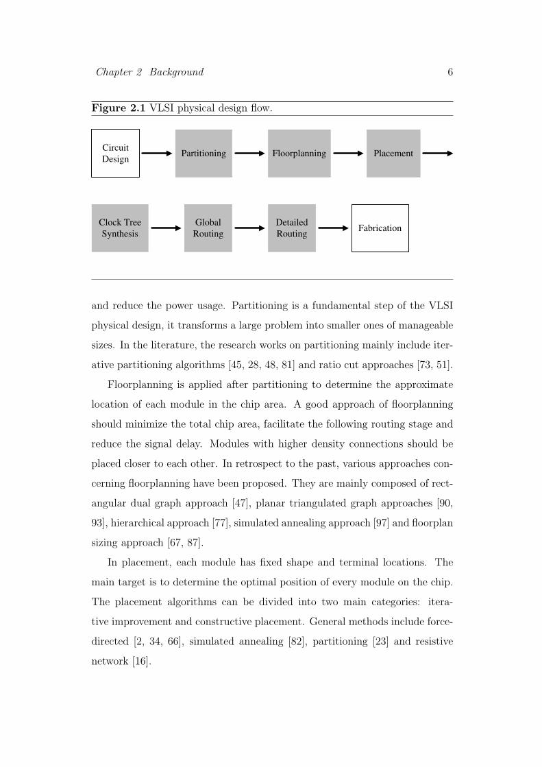
Figure 2.1 VLSI physical design flow.
Circuit
DesignPartitioning Floorplanning Placement
Clock Tree
Synthesis
Global
Routing
Detailed
RoutingFabrication
and reduce the power usage. Partitioning is a fundamental step of the VLSI
physical design, it transforms a large problem into smaller ones of manageable
sizes. In the literature, the research works on partitioning mainly include iter-
ative partitioning algorithms [45, 28, 48, 81] and ratio cut approaches [73, 51].
Floorplanning is applied after partitioning to determine the approximate
location of each module in the chip area. A good approach of floorplanning
should minimize the total chip area, facilitate the following routing stage and
reduce the signal delay. Modules with higher density connections should be
placed closer to each other. In retrospect to the past, various approaches con-
cerning floorplanning have been proposed. They are mainly composed of rect-
angular dual graph approach [47], planar triangulated graph approaches [90,
93], hierarchical approach [77], simulated annealing approach [97] and floorplan
sizing approach [67, 87].
In placement, each module has fixed shape and terminal locations. The
main target is to determine the optimal position of every module on the chip.
The placement algorithms can be divided into two main categories: itera-
tive improvement and constructive placement. General methods include force-
directed [2, 34, 66], simulated annealing [82], partitioning [23] and resistive
network [16].
Chapter 2 Background 7
The major target of clock network synthesis is to connect all the syn-
chronous signal receivers together with the signal source. Buffer insertion,
sizing and wire customization are also engaged to synthesize the work and
further improve the timing performance. The basic two approaches of clock
tree construction are the top-down procedure [40] and the bottom-up proce-
dure [41]. There are also two general methods of signal delay computation:
linear delay estimated by wirelength and Elmore RC delay model [26].
In global routing, the grid is decomposed into small rectangles, which are
named global bins. Only inter-bin connection among the pins of each network
is applied in global routing. It is aimed at reducing the degree of conges-
tion and the total wirelength. A good global router will evenly distribute
the congestion over the whole routing area. The general routing methods in-
clude multi-commodity flow-based approaches [6, 85] and single-turn routing
approach [43].
Detailed routing follows the global routing and implements the intercon-
nections inside the global bins. Track assignment between global bins is also
completed. The general approaches include channel routing [78] and hierar-
chical routing [4].
2.2 Metrics Analysis
In this section, we introduce the major metrics for performance evaluation
in this thesis. Generally, the evaluation is based on the result regarding two
items: (1) timing delay (2) power consumption. Both of the two metrics should
be minimized in order to improve the performance of our research work.
2.2.1 Signal Delay Models
In clock tree synthesis, there are plenty of delay models in different orders.
By applying these models, signal delay at any point of the clock network can
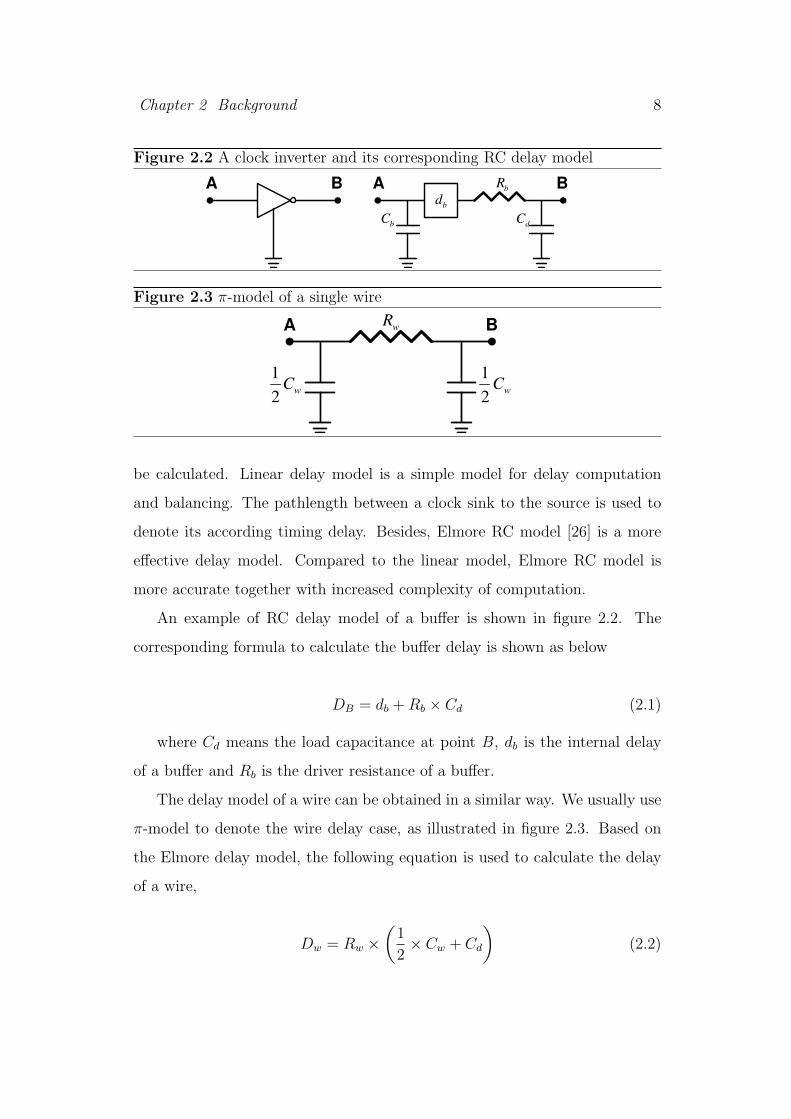
Chapter 2 Background 8
Figure 2.2 A clock inverter and its corresponding RC delay model
A BA B
bC
dC
bR
bd
Figure 2.3 π-model of a single wire
A B
1
2wC
1
2wC
wR
be calculated. Linear delay model is a simple model for delay computation
and balancing. The pathlength between a clock sink to the source is used to
denote its according timing delay. Besides, Elmore RC model [26] is a more
effective delay model. Compared to the linear model, Elmore RC model is
more accurate together with increased complexity of computation.
An example of RC delay model of a buffer is shown in figure 2.2. The
corresponding formula to calculate the buffer delay is shown as below
DB = db + Rb × Cd (2.1)
where Cd means the load capacitance at point B, db is the internal delay
of a buffer and Rb is the driver resistance of a buffer.
The delay model of a wire can be obtained in a similar way. We usually use
π-model to denote the wire delay case, as illustrated in figure 2.3. Based on
the Elmore delay model, the following equation is used to calculate the delay
of a wire,
Dw = Rw ×
(
1
2× Cw + Cd
)
(2.2)
Chapter 2 Background 9
where Cd denotes the load capacitance at point B, Rw denotes the unit
resistance of a wire and Cw denotes the unit capacitance of a wire.
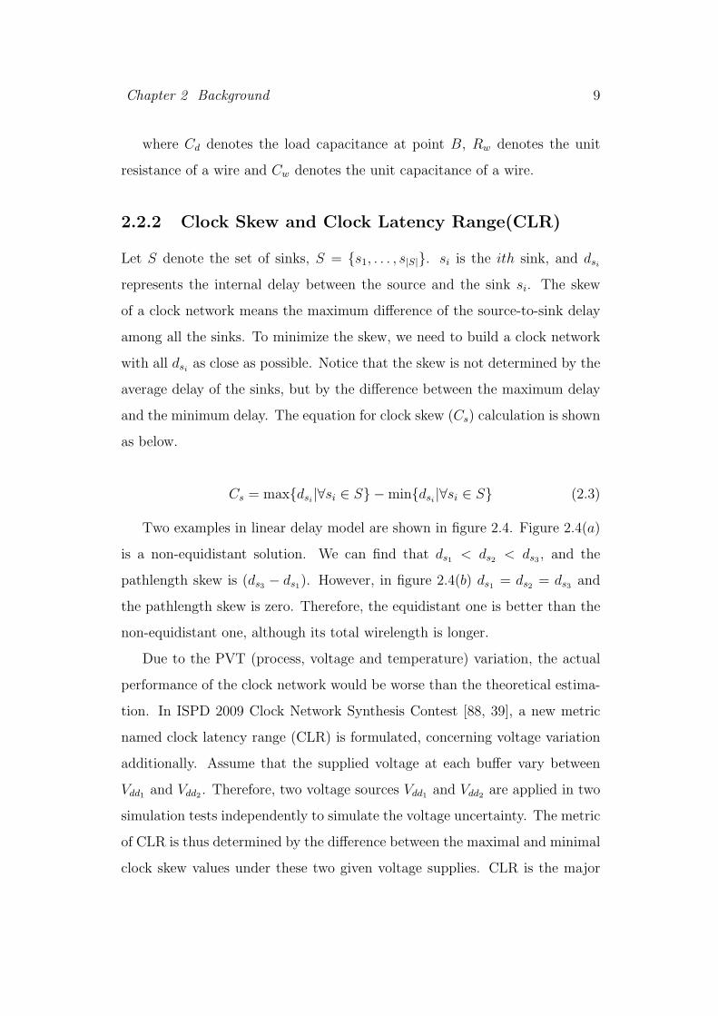
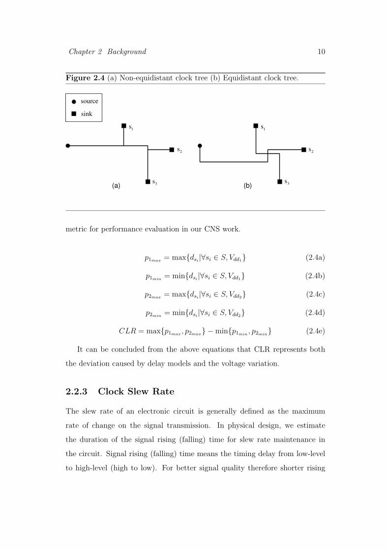
2.2.2 Clock Skew and Clock Latency Range(CLR)
Let S denote the set of sinks, S = s1, . . . , s|S|. si is the ith sink, and dsi
represents the internal delay between the source and the sink si. The skew
of a clock network means the maximum difference of the source-to-sink delay
among all the sinks. To minimize the skew, we need to build a clock network
with all dsias close as possible. Notice that the skew is not determined by the
average delay of the sinks, but by the difference between the maximum delay
and the minimum delay. The equation for clock skew (Cs) calculation is shown
as below.
Cs = maxdsi|∀si ∈ S − mindsi
|∀si ∈ S (2.3)
Two examples in linear delay model are shown in figure 2.4. Figure 2.4(a)
is a non-equidistant solution. We can find that ds1< ds2
< ds3, and the
pathlength skew is (ds3− ds1
). However, in figure 2.4(b) ds1= ds2
= ds3and
the pathlength skew is zero. Therefore, the equidistant one is better than the
non-equidistant one, although its total wirelength is longer.
Due to the PVT (process, voltage and temperature) variation, the actual
performance of the clock network would be worse than the theoretical estima-
tion. In ISPD 2009 Clock Network Synthesis Contest [88, 39], a new metric
named clock latency range (CLR) is formulated, concerning voltage variation
additionally. Assume that the supplied voltage at each buffer vary between
Vdd1and Vdd2
. Therefore, two voltage sources Vdd1and Vdd2
are applied in two
simulation tests independently to simulate the voltage uncertainty. The metric
of CLR is thus determined by the difference between the maximal and minimal
clock skew values under these two given voltage supplies. CLR is the major
Chapter 2 Background 10
Figure 2.4 (a) Non-equidistant clock tree (b) Equidistant clock tree.
1s
2s
3s
1s
2s
3s
source
sink
(a) (b)
metric for performance evaluation in our CNS work.
p1max= maxdsi
|∀si ∈ S, Vdd1 (2.4a)
p1min= mindsi
|∀si ∈ S, Vdd1 (2.4b)
p2max= maxdsi
|∀si ∈ S, Vdd2 (2.4c)
p2min= mindsi
|∀si ∈ S, Vdd2 (2.4d)
CLR = maxp1max, p2max
− minp1min, p2min
(2.4e)
It can be concluded from the above equations that CLR represents both
the deviation caused by delay models and the voltage variation.
2.2.3 Clock Slew Rate
The slew rate of an electronic circuit is generally defined as the maximum
rate of change on the signal transmission. In physical design, we estimate
the duration of the signal rising (falling) time for slew rate maintenance in
the circuit. Signal rising (falling) time means the timing delay from low-level
to high-level (high to low). For better signal quality therefore shorter rising
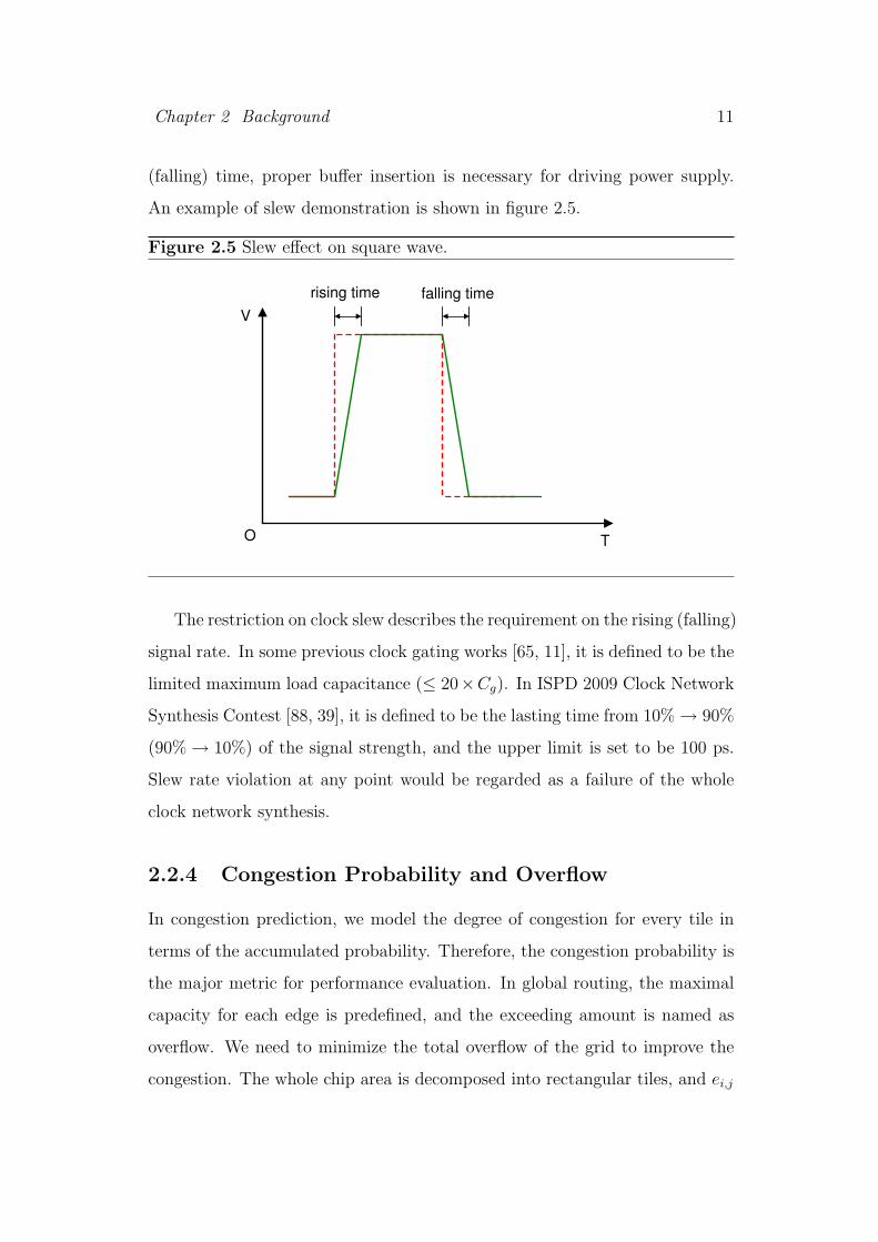
Chapter 2 Background 11
(falling) time, proper buffer insertion is necessary for driving power supply.
An example of slew demonstration is shown in figure 2.5.
Figure 2.5 Slew effect on square wave.
TO
V
rising time falling time
The restriction on clock slew describes the requirement on the rising (falling)
signal rate. In some previous clock gating works [65, 11], it is defined to be the
limited maximum load capacitance (≤ 20×Cg). In ISPD 2009 Clock Network
Synthesis Contest [88, 39], it is defined to be the lasting time from 10% → 90%
(90% → 10%) of the signal strength, and the upper limit is set to be 100 ps.
Slew rate violation at any point would be regarded as a failure of the whole
clock network synthesis.
2.2.4 Congestion Probability and Overflow
In congestion prediction, we model the degree of congestion for every tile in
terms of the accumulated probability. Therefore, the congestion probability is
the major metric for performance evaluation. In global routing, the maximal
capacity for each edge is predefined, and the exceeding amount is named as
overflow. We need to minimize the total overflow of the grid to improve the
congestion. The whole chip area is decomposed into rectangular tiles, and ei,j

Chapter 2 Background 12
Figure 2.6 The tracks between tile T1 and tile T2.
track
tile T1 tile T2
denotes the edge connecting the two adjacent tiles Ti and Tj. The respective
capacity, demand and overflow on this edge are denoted as capi,j, demi,j and
ovfi,j, respectively. ovftotal means the total overflow of the whole circuit. The
capacity of an edge is determined by the number of tracks on it. As shown in
figure 2.6, the red double-arrow line denotes a single track. Since there are six
tracks in all on e1,2, we have cap1,2 = 6. There will be overflow if the according
demand of tracks dem1,2 exceeds the capacity. The general definition of ovfi,j
and ovftotal are shown as below.
ovfi,j =
demi,j − capi,j : demi,j > capi,j
0 : demi,j ≤ capi,j
(2.5)
ovftotal =∑
all ei,j
ovfi,j (2.6)
2.2.5 Power on Capacitance and Wirelength
Power consumption has become a critical issue in the system-on-chip (SoC)
design. Besides previous research works, much more work remains to be done
Chapter 2 Background 13
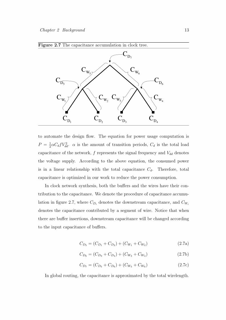
Figure 2.7 The capacitance accumulation in clock tree.
1DC
1WC2WC
2DC3DC
3WC4WC
4DC
5WC6WC
5DC
7DC
6DC
to automate the design flow. The equation for power usage computation is
P = 12αCdfV 2
dd. α is the amount of transition periods, Cd is the total load
capacitance of the network, f represents the signal frequency and Vdd denotes
the voltage supply. According to the above equation, the consumed power
is in a linear relationship with the total capacitance Cd. Therefore, total
capacitance is optimized in our work to reduce the power consumption.
In clock network synthesis, both the buffers and the wires have their con-
tribution to the capacitance. We denote the procedure of capacitance accumu-
lation in figure 2.7, where CDidenotes the downstream capacitance, and CWi
denotes the capacitance contributed by a segment of wire. Notice that when
there are buffer insertions, downstream capacitance will be changed according
to the input capacitance of buffers.
CD5= (CD1
+ CD2) + (CW1
+ CW2) (2.7a)
CD6= (CD3
+ CD4) + (CW3
+ CW4) (2.7b)
CD7= (CD5
+ CD6) + (CW5
+ CW6) (2.7c)
In global routing, the capacitance is approximated by the total wirelength.
Chapter 2 Background 14
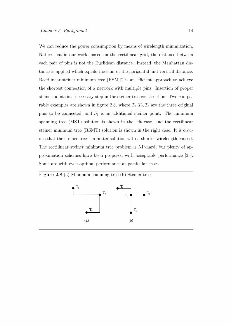
We can reduce the power consumption by means of wirelength minimization.
Notice that in our work, based on the rectilinear grid, the distance between
each pair of pins is not the Euclidean distance. Instead, the Manhattan dis-
tance is applied which equals the sum of the horizontal and vertical distance.
Rectilinear steiner minimum tree (RSMT) is an efficient approach to achieve
the shortest connection of a network with multiple pins. Insertion of proper
steiner points is a necessary step in the steiner tree construction. Two compa-
rable examples are shown in figure 2.8, where T1, T2, T3 are the three original
pins to be connected, and S1 is an additional steiner point. The minimum
spanning tree (MST) solution is shown in the left case, and the rectilinear
steiner minimum tree (RSMT) solution is shown in the right case. It is obvi-
ous that the steiner tree is a better solution with a shorter wirelength caused.
The rectilinear steiner minimum tree problem is NP-hard, but plenty of ap-
proximation schemes have been proposed with acceptable performance [35].
Some are with even optimal performance at particular cases.
Figure 2.8 (a) Minimum spanning tree (b) Steiner tree.
(a) (b)
1T
2T
3T
1T
2T
3T
1S
Chapter 3
Literature Review
3.1 Overview
In this thesis, our research focus is located at the routability in VLSI physical
design. During the early designing time, congestion prediction is applied in
order to evaluate the degree of congestion in terms of respective probability on
edge occupancy. In clock network synthesis, buffers cannot be inserted inside
the blockage areas, which are preoccupied by macro blocks during the place-
ment stage. Therefore, routability is maintained by proper buffer distribution
for clock signal transmission. Clock gating design is an associating step of CNS
aiming at power reduction. It is implemented by turn on/off active/inactive
modules selectively. Subsequently except for the clock network, global routing
implements the connection of the rest of the networks inside the chip area.
Congestion and overflow are minimized and the according routability is max-
imized.
3.2 Congestion Prediction
By virtue of the non-stopping reduction of feature size in the VLSI design, in-
terconnection delay replaces the transistor delay to be the dominant factor on
15
Chapter 3 Literature Review 16
the signal delay. Therefore, routability has become a critical concern regard-
ing the total timing performance of the circuit. However, improper design or
operation in early stages will cause negative effect to the routing performance.
For instance, arbitrary packing of modules will possibly lead to uneven distri-
bution of congestion. As a result, the interconnection of such placement result
may not be completed by global routers. Therefore, it is quite necessary to
develop algorithms to improve routability during the placement or some other
early designing steps, where congestion prediction is an effective technique of
them. Congestion prediction can provide the probability of usage of all the
tiles on the chip.
In retrospect to the past research achievements, several models have been
proposed. In the works [14, 7, 57], a packing is divided into tiles and conges-
tion is estimated in each tile, assuming that each net is routed in either L- or
Z-shape. In [50], the congestion model used is the average net density on the
boundaries of different regions in a floorplanning. In the papers [49, 54], prob-
abilistic analysis is performed to estimate congestion and routability. They
assume that all feasible routes have the same probability of being selected. In
practice, routes of less bends are more desirable. In the papers [42, 96], ex-
tended versions of [54] are proposed. The authors take into account the impact
of the number of bends in a routing path on the probability of occurrence of
the path. However, the accuracy of their congestion models will depend on
the accuracies of their predictions on the distribution of the number of bends
in the routed circuit. The paper [99] proposed to predict congestion by using
the Rent’s rule. However, connections of the nets are already known in the
floorplanning and placement stage, and we should be able to predict conges-
tion more accurately than simply using the Rent’s rule. The papers [94, 95]
proposed to use global routers to estimate congestion, which will be more accu-
rate but the runtime penalty is high. The paper [75] presented a probabilistic
congestion prediction method based on routers intelligence. The paper [89]
Chapter 3 Literature Review 17
gives an tutorial on all recent congestion technique and show the importance
of the congestion prediction.
3.3 Clock Network Synthesis
After placement, the interconnection of all the networks should be completed in
the stage of routing, in which clock network synthesis is the first step. In VLSI
circuits, digital modules are synchronized by receiving clock signals, which are
transmitted from a source through the clock network. In clock network synthe-
sis, the clock skew is usually a major concern, which represents the difference of
the signal arrival time at all the terminals. In order to synchronize one circuit,
each terminal must be reached by the clock signal within a small time range.
Otherwise, the performance on synchronization is unacceptable. Regarding
the maximum attainable frequency of operation in the circuits, the resultant
clock skew of the synthesis work must be reduced into a predetermined range.
Clock skew minimization is a popular research topic during the past decades.
Plenty of research achievements have been proposed by previous researchers.
Some earlier proposed works concentrated on the distribution of wirelength
between the source and the sinks to achieve delay equalization. Jackson [40]
firstly presented a clock routing algorithm in a top-down course. Later, a geo-
metric perfect matching was proposed in [41] in a bottom-up procedure. More
improvements were also made to reach exact equidistant tree [25] for the clock
network. Afterwards, delay balancing using Elmore delay model [26] became
prevalent to acquire more accurate information on the timing delay. Clock tree
with exact zero skew [92] was proposed by applying such balancing method.
The deferred-merging and embedding (DME) technique [3, 10] was proposed
to achieve zero skew with a shorter wirelength in the clock tree. In topol-
ogy generation, some algorithms were proposed for both un-buffered [24] and
buffered [12] clock trees respectively. In [31, 17] buffer insertion was involved
Chapter 3 Literature Review 18
for power supply and transition time reduction
In the recent years, tolerance on variation became a focus of attention. This
is mainly due to the uncertainty of various uncertain factors inside a circuit,
such as process [63, 100], voltage [76] and temperature [80]. In order to keep
a chip stable and functioning well, methods with greater tolerance on varia-
tion are widely favored. Many researchers focused on robust algorithms for
variation minimization. Techniques such as wire sizing [52], buffer sizing [15]
and link insertion [71, 72] are applied. In ISPD 2009 clock network synthesis
contest [88, 39], a voltage variation related objective, CLR, was formulated.
Several new benchmarks were released accordingly. Subsequently, some re-
lated research works were proposed [86, 53, 55]. In [55], a dual-MST topology
generation approach was devised and analyzed Its objective is to minimize the
maximal edge cost during the weighted perfect matching.
3.4 Clock Gating Design
In modern VLSI design, optimization on the power consumption is necessary, in
case chip overheat and battery shortage (for portable devices). Clock network
affords the synchronization of digital modules in the circuits. However, it is also
quite power consuming. From statistics, it is shown that twenty to fifty percent
of the dynamic power usage is contributed by the clock network [46]. Therefore,
optimization on clock network is an effective way to make the chip less power
consuming. At each clock period, only a small portion of the digital module set
is active. The remaining modules are temporarily idle and they can be turned
off for power saving. Based on this assumption, gated clock network is proposed
in the sequential circuits for enable/disable control signal transmission. The
principal idea is to turn off the idle modules and the according sections of the
clock tree, and the unnecessary switching power can thus be cut down.
Clock gating can be applied on logic level [8], register-transfer-level level [22]
Chapter 3 Literature Review 19
and architecture level [56], respectively. Nevertheless, optimization on these
upper design levels may ignore the physical information and cause unnecessary
detours or snaking wires. Upper level improvement may be offsetted by lower
level implementation [30]. As a matter of fact, physical location of the modules
should be taken into account during the clock gating design, in case wirelength
overhead thus power waste.
Some achievements have been proposed with simultaneous logical and phys-
ical concerns. The design of activity-driven gated clock network was proposed
in [91] and [27]. However, clock skew was only concerned by gate number
balancing, and the contribution of wires were ignored. Meanwhile, the gate
insertion was not applied concurrently within the topology generation. In [13],
similarity of activity patterns between clock nodes was utilized, and the per-
formance was improved with reduced power consumption. Instruction stream
was proposed in [64] to simulate the probabilistic information of each mod-
ule. In [65], a gating method regarding microprocessor design was developed
to minimize the switched capacitance. However, no relationship of activities
was concerned while merging each pair of nodes. Meanwhile, the resulted clock
tree was still non-zero skew. Recently, a comprehensive technique was proposed
in [11]. It is composed of a recursive computation on effective switched capaci-
tance and a solution sampling method based on merging segment set. Despite
the improvement on performance, the approach is very time and memory con-
suming, and the slew rate is too ideal (limit on downstream capacitance) which
may not be applicable for industry use.
3.5 Global Routing
After clock network synthesis, global routing and detailed routing are applied
to complete the interconnections of the rest of the networks. In the stage of
Chapter 3 Literature Review 20
global routing, the grid is decomposed into global bins. By such decomposi-
tion, all the pins are labelled with the coordinates of their according global
bins. In each network, only the pins from different global bins need to be con-
nected together. The specific inner-bin connection will be implemented in the
detailed routing. Plenty of research works regarding global routing have been
proposed with a great deal of improvements achieved [60]. Meanwhile, there
were two global routing contests held in 2007 [62, 37] and 2008 [38], which
greatly stimulated the research interests in global routing.
Among those state-of-the-art global routers, they generally employ two
categories of basic techniques: (1) iterative rip-up and rerouting (2) multi-
commodity flow. The approach of iterative rip-up and rerouting does not
confine routing selections in the early steps. However, it completes the task
by means of numerous iterations of rerouting to gradually approach the fi-
nal target of zero overflow. Repetitious rerouting would cost additional run-
time to fulfill the work, thus focus is usually centralized on those congested
area to make the processing efficient. The distribution of routing power is
asymmetrical among all the nets, and congested nets usually get a big share.
There are already a number of algorithms proposed based on it. Chi Dis-
persion [32] is a global routing approach implemented based on cost ampli-
fication. Labyrinth [44] is implemented based on the scheme of predictable
routing. These are the two early global routers employing this technique.
Recently, more and more global routers are presented, including Archer [68],
BoxRouter [18], FGR [74], FastRoute [69, 70, 101], MaizeRoute [58, 59], NTHU-
Route[29, 9], NTUgr [33] and NCTU [21]. Most of them apply FLUTE [19, 20],
a rather efficient tool based on look-up table, to generate the Rectilinear Steiner
Minimum Tree (RSMT) for each network. FastRoute is of rather high speed
and it can be integrated into placement to provide interconnection information.
MaizeRoute is implemented with extreme-edge-shift technique, and NTHU

Chapter 3 Literature Review 21
uses the concept of region-based constraint for overflow reduction. For the ap-
proach of multi-commodity flow, the global routing problem is formulated and
transferred into an integer linear programming (ILP) problem to be solved. A
recent router from the work by Albrecht [1] provides an approximation method
based on this approach.
3.6 Summary
From the above review, it is shown that some achievements have been made
by previous researchers on the topic of routability. Nevertheless, owing to
the development of the craft on semiconductors and the enlargement of the
integration scale, new requirements on routability have been proposed. There-
fore, there are still large space for performance improvement. In congestion
estimation, a lot of efficient models have been proposed, such as some prede-
fined patterns for resource assignment and probabilistic analysis. The influence
caused by routing procedure still lacks enough concerns. In clock network syn-
thesis and clock gating design, equidistant clock tree and zero skew approach
have been developed and improved. Nonetheless, excessive focus on wirelength
optimization would deteriorate the tolerance on variability and reduce the ro-
bustness of the work. In global routing, recent global routers focused on fast
reduction of overflow, but the optimization on wirelength and via connection
is partly ignored.
Chapter 4
Congestion Prediction
4.1 Overview
Congestion prediction is of crucial importance in the early stages of the physical
design. In this chapter, we propose three congestion models: SMD (shortest
Manhattan distance), Detour model [84] and 3-step approach [83]. From the
experimental results it is shown that the 3-step approach is the most efficient
one considering the accuracy of congestion prediction.
4.2 Problem Formulation
Congestion modeling is an important part of interconnect estimation during
the floorplanning and placement stage. Given a packing which is partitioned
into lh × lw tiles (according to the length of tile, tl), we will calculate the net
density at each tile according to the congestion model. Net density means the
accumulated probability of tracking paths in each tile, which are contributed
by all the nets in the chip. Based on the congestion information obtained
from the net density, we can evaluate the routability of the packing result.
The objective of our work is to minimize the difference between the results of
estimation and routing, in order to predict the grade of congestion accurately
at early stages of the physical design.
22

Chapter 4 Congestion Prediction 23
Table 4.1 Notations in congestion prediction
Notation Descriptiontl Length of a tile
chmax Maximum horizontal wire capacity inside a tile
cvmax Maximum vertical wire capacity inside a tile
ck(r) The number of tiles that is r tiles from the source of net kDTk The shortest Manhattan distance between the source and sink of
the net kdk(x, y) The distance from the source of net k to tile (x, y)Pk(x, y) A rough estimation of the probability of net k passing through
the tile (x, y)W (x, y) The weight of tile (x, y)
CFk Congestion factor of the net klkd Detoured length of the net k
Ek(x, y) Probability of net k passing through (x, y)Eh
k (x, y) Probability of net k passing through (x, y) horizontallyEv
k(x, y) Probability of net k passing through (x, y) verticallyEh(x, y) Expected number of wires passing through (x, y) horizontallyEv(x, y) Expected number of wires passing through (x, y) verticallyAh(x, y) Actual number of wires passing through (x, y) horizontally,
obtained from global routing resultAv(x, y) Actual number of wires passing through (x, y) vertically,
obtained from global routing result(sx
k, syk) Coordinate of the source tile of net k
(txk, tyk) Coordinate of the terminal tile of net k
T dk The set of extra tiles when the detoured nets pass through
outside the bounding box of net kTk The set of tiles inside the bounding box of net k
Tk(d) The set of tiles inside the bounding box of net k,being d tiles away from the source
Chapter 4 Congestion Prediction 24
4.3 Analysis of Congestion Models
In the previous works regarding congestion prediction, we usually break down
the multi-pin nets into 2-pin nets first. A network with N pins can be de-
composed into N − 1 subnets, each subnet is a connection of two pins. In
this section, we mainly propose three models of congestion prediction. All of
them are constructed based on 2-pin subnets decomposition. Respective prin-
cipal analysis and performance comparison are listed. These models are SMD,
Detour and 3-step approach, which are discussed as follows.
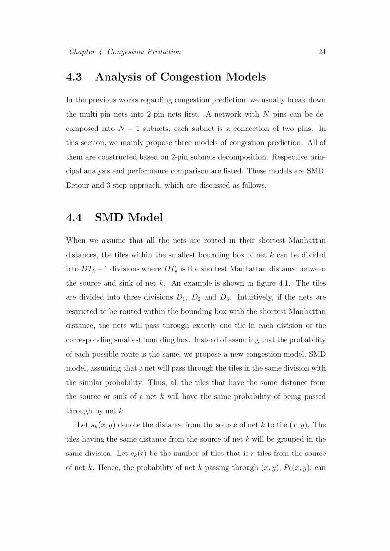
4.4 SMD Model
When we assume that all the nets are routed in their shortest Manhattan
distances, the tiles within the smallest bounding box of net k can be divided
into DTk − 1 divisions where DTk is the shortest Manhattan distance between
the source and sink of net k. An example is shown in figure 4.1. The tiles
are divided into three divisions D1, D2 and D3. Intuitively, if the nets are
restricted to be routed within the bounding box with the shortest Manhattan
distance, the nets will pass through exactly one tile in each division of the
corresponding smallest bounding box. Instead of assuming that the probability
of each possible route is the same, we propose a new congestion model, SMD
model, assuming that a net will pass through the tiles in the same division with
the similar probability. Thus, all the tiles that have the same distance from
the source or sink of a net k will have the same probability of being passed
through by net k.
Let sk(x, y) denote the distance from the source of net k to tile (x, y). The
tiles having the same distance from the source of net k will be grouped in the
same division. Let ck(r) be the number of tiles that is r tiles from the source
of net k. Hence, the probability of net k passing through (x, y), Pk(x, y), can
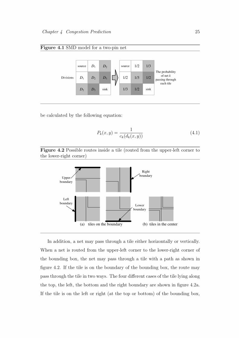
Chapter 4 Congestion Prediction 25
Figure 4.1 SMD model for a two-pin net
D3D2
D1 D3
D2
D2
D1
1/3 1/2
1/2 1/3
1/2 1/3
1/2
The probability
of net k
passing through
each tile
source
sink
Divisions
source
sink
be calculated by the following equation:
Pk(x, y) =1
ck(dk(x, y))(4.1)
Figure 4.2 Possible routes inside a tile (routed from the upper-left corner tothe lower-right corner)
Right
boundaryUpper
boundary
Left
boundaryLower
boundary
(a) tiles on the boundary (b) tiles in the center
In addition, a net may pass through a tile either horizontally or vertically.
When a net is routed from the upper-left corner to the lower-right corner of
the bounding box, the net may pass through a tile with a path as shown in
figure 4.2. If the tile is on the boundary of the bounding box, the route may
pass through the tile in two ways. The four different cases of the tile lying along
the top, the left, the bottom and the right boundary are shown in figure 4.2a.
If the tile is on the left or right (at the top or bottom) of the bounding box,
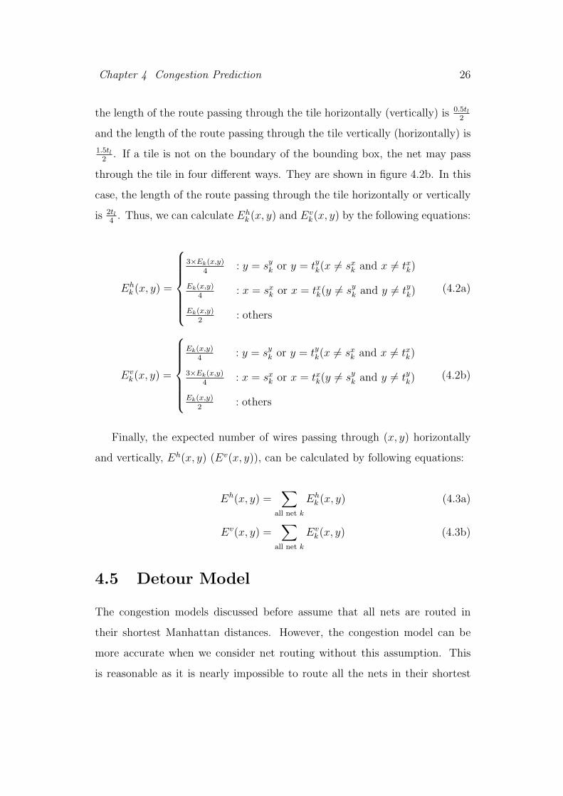
Chapter 4 Congestion Prediction 26
the length of the route passing through the tile horizontally (vertically) is 0.5tl2
and the length of the route passing through the tile vertically (horizontally) is
1.5tl2
. If a tile is not on the boundary of the bounding box, the net may pass
through the tile in four different ways. They are shown in figure 4.2b. In this
case, the length of the route passing through the tile horizontally or vertically
is 2tl4
. Thus, we can calculate Ehk (x, y) and Ev
k(x, y) by the following equations:
Ehk (x, y) =
3×Ek(x,y)4
: y = syk or y = tyk(x 6= sx
k and x 6= txk)
Ek(x,y)4
: x = sxk or x = txk(y 6= sy
k and y 6= tyk)
Ek(x,y)2
: others
(4.2a)
Evk(x, y) =
Ek(x,y)4
: y = syk or y = tyk(x 6= sx
k and x 6= txk)
3×Ek(x,y)4
: x = sxk or x = txk(y 6= sy
k and y 6= tyk)
Ek(x,y)2
: others
(4.2b)
Finally, the expected number of wires passing through (x, y) horizontally
and vertically, Eh(x, y) (Ev(x, y)), can be calculated by following equations:
Eh(x, y) =∑
all net k
Ehk (x, y) (4.3a)
Ev(x, y) =∑
all net k
Evk(x, y) (4.3b)
4.5 Detour Model
The congestion models discussed before assume that all nets are routed in
their shortest Manhattan distances. However, the congestion model can be
more accurate when we consider net routing without this assumption. This
is reasonable as it is nearly impossible to route all the nets in their shortest

Chapter 4 Congestion Prediction 27
Manhattan distances for any large circuit. In this section, we will also pro-
pose a new congestion model (called Detour model [84]) in which each net
is not necessarily routed in its shortest Manhattan distance. Detour model is
proposed based on the SMD model. It assumes that a route may have detours.
4.5.1 Estimation of Detoured length
Table 4.2 Percentage of detoured nets
In this section, we show how to estimate the congestion of the tiles when
nets may detour. Obviously, the nets may detour only when some locations of
the packings are very congested. We perform global routing on the packings to
illustrate the percentage of detoured nets under different routing environments.
The experimental results are shown in table 4.2. We can see that if the packing
is more congested, more nets may detour. Thus, we can first use SMD model
to evaluate the congestion of the packing and calculate the congestion factor
of each net k by following equation:
CFk =∑
(x,y)∈T
2 × (Eh(x, y) − Ehk (x, y) + Ev(x, y) − Ev
k(x, y))
|skx − tkx| + 1 × |sk
y − tky| + 1× (ch
max + cvmax)
(4.4)
where skx ≤ x ≤ tkx and sk
y ≤ y ≤ tky.
From the equation, we can see that if CFk is larger than one, it means that
the bounding box is very congested for net k and the net k may likely detour.
Chapter 4 Congestion Prediction 28
Thus, we can estimate the length of detour of net k by the following equation
(if lkd is smaller than zero, it is adjusted to zero):
lkd = ⌊(CFk − 1) × DTk⌋ (4.5)
Table 4.3 Improvement of wirelength estimation
We have performed global routing on the packings to verify the estimation
of detoured length. The experimental results are shown in table 4.3. From the
experiments, we can see the error between our estimated wirelength (the multi-
pin nets are decomposed into 2-pins nets by rectilinear minimum spanning tree
first) and the actual wirelength by global routing is always smaller than the
error between the wirelength of rectilinear minimum spanning tree (RMST)
and the actual wirelength. It means that we can always estimate the wirelength
more accurately by using congestion factor.
4.5.2 Congestion Estimation
As the detoured nets may pass through outside the bounding box, some extra
tiles may be passed through by those nets. These extra tiles are the tiles
when the detoured nets pass through outside the bounding box of net k with
detoured length less than lkd . First, we define T dk as those extra tiles for a
net k. In real cases, Pk(x, y) for (x, y) ∈ T dk will depend on the location of
the congestion area. Detours happen because of some random over-congested
tiles. Because of this random situation, it is reasonable to assume that all tiles

Chapter 4 Congestion Prediction 29
Figure 4.3 Detour model for a two-pin net
D3
D2
D1
D3
D2
D2
D1
1-2c
2
1-2c
2
1-2c
3
The probability of net k (detoured length is 2)
passing through each tile
source
sink
Divisions
source
1-2c
2
Tdk T
dk T
dk
Tdk
Tdk
Tdk
TdkT
dkT
dk
Tdk
Tdk
Tdk
c
c
c c
c
c
c
ccc
c
c
Tdk
Tdk
D3
D4
D4
c
c
1
4
1-2c
2
sink
D5
D3
D4 D5 cc
1-2c
3
1-2c
3
1-2c
3
1-2c
3
1-2c
3
1
4
1
4
1
4
TdkT
dk
(x, y) in T dk have the same probability. Hence, we can build the congestion
map based on SMD model. An example is shown in figure 4.3.
The detoured net may often pass through outside the bounding box with
less bends. If edge shifting [69] is used, the most common case is that either the
whole vertical or horizontal path is outside the bounding box. Thus, either
all horizontal segments or all vertical segments are passing through outside
the bounding box. In this case, we assume that half of the wirelength of the
detoured net will be contributed by the tile in T dk .
The detoured net may often pass through outside the bounding box with
less bends. The most common case is that either the whole vertical or hor-
izontal path is outside the bounding box. Thus, we assume that half of the
wirelength of the detoured net will be contributed by the tile in T dk . Hence,
we can calculate Pk(x, y) where (x, y) ∈ T dk by following equation:
Ek(x, y) =DTk + lkd2 × |T d
k |: (x, y) ∈ T d
k (4.6)
where |T dk | is the number of tiles in T d
k
Chapter 4 Congestion Prediction 30
Hence, we can calculate Ek(x, y) of other tiles (for any (x, y) /∈ T dk ) that
inside the bounding box following equation:
Ek(x, y) =1 − c ∗ |T d
k |sk(x,y)
ck(sk(x, y))(4.7)
where |T dk |sk(x,y) is the number of tiles in same diagonal of the division sk(x, y)
and c is Ek(x, y) for any (x, y) ∈ T dk . In addition, a net may pass through a
tile either horizontally or vertically. We will calculate Ehk (x, y) and Ev
k(x, y)
by equation 4.2.
4.6 3-Step Approach
The estimation process is divided into three steps: preliminary estimation,
detailed estimation and congestion redistribution. To avoid over-estimating
congestion, we perform a preliminary estimation step first to determine which
regions are likely to be over-congested. A region should be more attractive to
net routing if it is less congested. Then, we will make use of this information to
predict the congestion measures during the detailed estimation step. We use a
SMD model described in section 4.4 because of its simplicity and experimental
results have shown that this model can give accurate estimations. Finally,
congestion redistribution will be performed to simulate the rip-up and reroute
operations of the detailed routing step by moving wires from over-congested
regions to less congested regions. We use a 3-step approach [83] as follows:
• Preliminary Estimation: We estimate the congestion measure at each
tile roughly according to the bounding box of each net so that we can
determine which regions are likely to be over-congested.
• Detailed Estimation: Based on the information obtained from the pre-
liminary estimation step, we estimate the congestion measure at each tile
by using a diagonal-based congestion model.

Chapter 4 Congestion Prediction 31
• Congestion Redistribution: We will simulate the rip-up and reroute pro-
cess of the routing stage by moving wires from over-congested tiles to
less congested tiles.
4.6.1 Preliminary Estimation
In practice, we will choose to route a net over the tiles that are less congested to
prevent overflow. It means that some tiles are more attractive to net routing
and some tiles are less. However, this fact is usually ignored in traditional
congestion models. In our approach, a preliminary estimation of the congestion
map will be performed to obtain this information. If a rough estimation of the
congestion measure of a tile, P (x, y), is above the maximum wire capacity, the
tile (x, y) will be less attractive to net routing. On the other hand, if P (x, y) is
well below the maximum wire capacity, the tile (x, y) will be more attractive to
net routing. We will make use of these P (x, y) values to improve the accuracy
of the detailed estimation step.
In this preliminary estimation step, we assume that all the tiles inside the
bounding box of a net k, Tk, have the same probability, Pk(x, y), of being passed
through by net k. In addition, we assume that the nets can be routed in their
shortest Manhattan distances. The wirelength and the area of the bounding
box can be computed as |txk−sxk|+ |tyk−sy
k|+1 and (|txk−sxk|+1)×(|tyk−sy
k|+1)
respectively. Pk(x, y) can thus be calculated by the following equation:
Pk(x, y) =|txk − sx
k| + |tyk − syk| + 1
(|txk − sxk| + 1) × (|tyk − sy
k| + 1)(4.8)
We can then obtain a preliminary estimation by adding up the congestion
measures due to different nets:
P (x, y) =∑
all k
Pk(x, y) (4.9)
Chapter 4 Congestion Prediction 32
Figure 4.4 An example of computing the congestion measures for a two-pinnet in the detailed estimation step
0.4 0.5
0.5 0.4
0.5 0.2
0.5
The probability of net k
passing through each tile
Divisions
source
sink0.51
1 0.5
0.5
1
1source
sink
W(x, y)
8036
30 80
80
35
32source
sink
P(x, y) obtained from
preliminary estimation
chmax = 20
cvmax = 20
(p, q)
D3D2
D1 D3
D2
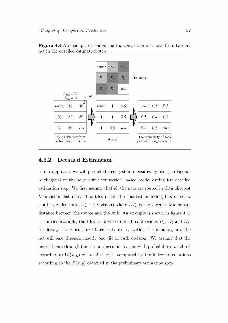
D2
D1source
sink
4.6.2 Detailed Estimation
In our approach, we will predict the congestion measures by using a diagonal
(orthogonal to the source-sink connection) based model during the detailed
estimation step. We first assume that all the nets are routed in their shortest
Manhattan distances. The tiles inside the smallest bounding box of net k
can be divided into DTk − 1 divisions where DTk is the shortest Manhattan
distance between the source and the sink. An example is shown in figure 4.4.
In this example, the tiles are divided into three divisions D1, D2 and D3.
Intuitively, if the net is restricted to be routed within the bounding box, the
net will pass through exactly one tile in each division. We assume that the
net will pass through the tiles in the same division with probabilities weighted
according to W (x, y) where W (x, y) is computed by the following equations
according to the P (x, y) obtained in the preliminary estimation step.
Chapter 4 Congestion Prediction 33
W (x, y) =
1 : P (x, y) < (chmax + cv
max)
chmax+cv
max
P (x,y): otherwise
(4.10)
If P (x, y) is smaller than the sum of chmax and cv
max, the tile (x, y) is unlikely
to be over-congested and so W (x, y) is 1. If P (x, y) is larger than the sum of
chmax and cv
max, that tile should have a smaller W (x, y) when P (x, y) is larger.
It reflects the case in the routing stage that the nets will be routed to pass
through less congested tiles. Hence, the probability of net k passing through
(x, y), Ek(x, y), can be calculated according to the weight of each tile, W (x, y),
by the following equation:
Ek(x, y) =W (x, y)
∑
(i,j)∈Tk(dk(x,y)) W (i, j)(4.11)
In the example of figure 4.4, chmax and cv
max are 20. When we focus on
division D2, (p, q) the tile at the upper right corner is a congested tile according
to the preliminary estimation step because P (p, q) is 80, which is larger than
the sum of chmax and cv
max. Thus, W (p, q) should be smaller than 1 and it is
computed as 0.5 according to equation 4.10. Hence, the probability of net k
passing through (p, q), Ek(p, q), is 0.2. It is smaller than the others in the same
division because the tile (p, q) is likely to be over-congested. In addition, a net
may pass through a tile either horizontally or vertically. We will calculate
Ehk (x, y) and Ev
k(x, y) by equation 4.2.
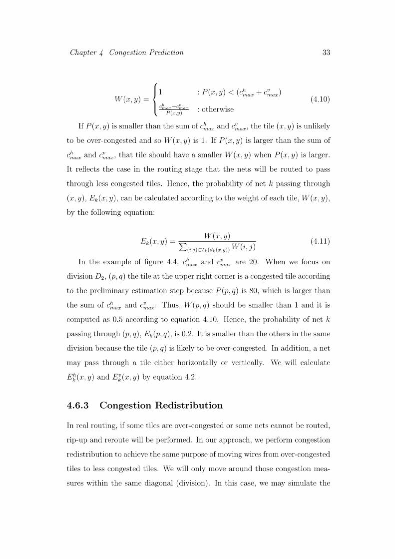
4.6.3 Congestion Redistribution
In real routing, if some tiles are over-congested or some nets cannot be routed,
rip-up and reroute will be performed. In our approach, we perform congestion
redistribution to achieve the same purpose of moving wires from over-congested
tiles to less congested tiles. We will only move around those congestion mea-
sures within the same diagonal (division). In this case, we may simulate the
Chapter 4 Congestion Prediction 34
routing process when less congested path is always selected and the total con-
gestion of one division can be maintained at one. An example is shown in
figure 4.5. In Tk(1) of net k, the tile with congestion estimation 7.2 is the most
congested in this division but it is not over-congested (less than the maximum
wire capacity of a tile). Thus, no action will be taken. In Tk(2), the tile with
12.4 is the most congested in this division and is over-congested. Thus, we will
move 0.2 (net k’s contribution to the congestion measure of this tile) from this
tile to the least congested tile of the same division.
Figure 4.5 An example of congestion redistribution
12.4 5.8
7.2 8.4
6.5 7.2
4.6
Congestion map after
detailed estimation
source
sink 12.2 5.8
7.2 8.4
6.5 7.4
4.6
Congestion map after
congestion redistribution
source
sink
This tile is the most
congested in the
division and it is
over-congested
Assume that the maximum wire capacity of a tile is 100.2
In general, we will find the tile, (xm, ym), with the maximum vertical (hori-
zontal) congestion and the tile, (xl, yl), with the minimum vertical (horizontal)
congestion from each division of all the nets. If the tile with the maximum
vertical (horizontal) congestion is over-congested, we will move Evk(xm, ym)
(Ehk (xm, ym)) from (xm, ym) to (xl, yl). After redistribution, the summation of
Evk(x, y) (Eh
k (x, y)) in the same division still equals one. Thus, the assumption
that each net will pass through exactly one tile in each division within the
bounding box still holds.

Chapter 4 Congestion Prediction 35
4.7 Experimental Results
In the experiments, the test cases used are the ISPD-02 suite circuits [36]. The
length of a tile, tl, is 40µm. The detailed information of the testing circuits
are shown in table 4.4. Our prediction models are robust approaches with no
inclusion of circuit-oriented parameter tuning. Therefore, the performance of
our work should be consistently good based on the packing results from various
placers. In our experiments, all the circuits are first placed using a wirelength
driven placer, Capo [5]. Four placement solutions are obtained for each test
case. Global routing is then performed on each placement solution by a maze
routing based global router [44]. During global routing, we set wiring capacity
value to simulate two environments: more congested and less congested cases.
For the data sets shown in table 4.5, there are about 0%− 2% over-congested
tiles after global routing. Different congestion models are then used to estimate
the congestion of the placed circuits and their estimations are then compared
with the actual congestion measures obtained from the global router.
Table 4.4 Information of the test cases
We compare our SMD model, Detour model and the 3-step approach with
Chapter 4 Congestion Prediction 36
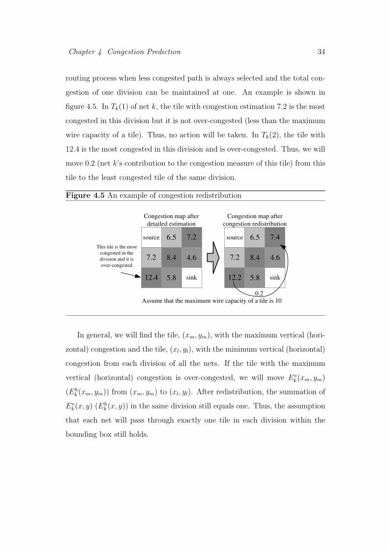
Table 4.5 Comparison on the mean and standard deviation of error of thecongestion models for more congested circuits
the models from Lou’s model [54] and Westra’s model [96]. We have im-
plemented all the congestion models and compared the estimations with the
results of the maze router. All programs were written in the C language and
run on a machine (Sun Blade 1000) with 750MHz processor and 2GB mem-
ory. We will compare the congestion models by calculating the mean of error,
µ and the standard deviation of error, µstd according the following equations:
µh =
∑
(x,y)∈T|Ah(x,y)−Eh(x,y)|
chmax
|T |
µv =
∑
(x,y)∈T|Av(x,y)−Ev(x,y)|
cvmax
|T |
µ =µh + µv
2(4.12)
Chapter 4 Congestion Prediction 37
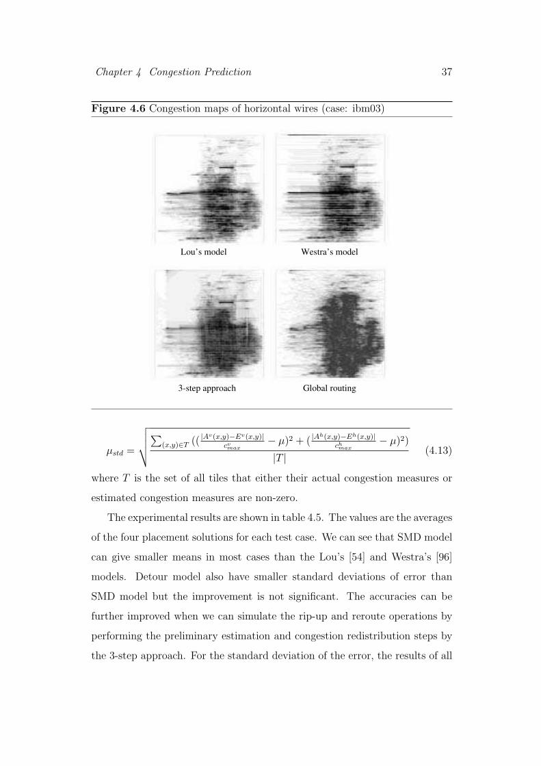
Figure 4.6 Congestion maps of horizontal wires (case: ibm03)
Lou’s model Westra’s model
3-step approach Global routing
µstd =
√
√
√
√
∑
(x,y)∈T (( |Av(x,y)−Ev(x,y)|
cvmax
− µ)2 + ( |Ah(x,y)−Eh(x,y)|
chmax
− µ)2)
|T |(4.13)
where T is the set of all tiles that either their actual congestion measures or
estimated congestion measures are non-zero.
The experimental results are shown in table 4.5. The values are the averages
of the four placement solutions for each test case. We can see that SMD model
can give smaller means in most cases than the Lou’s [54] and Westra’s [96]
models. Detour model also have smaller standard deviations of error than
SMD model but the improvement is not significant. The accuracies can be
further improved when we can simulate the rip-up and reroute operations by
performing the preliminary estimation and congestion redistribution steps by
the 3-step approach. For the standard deviation of the error, the results of all
Chapter 4 Congestion Prediction 38
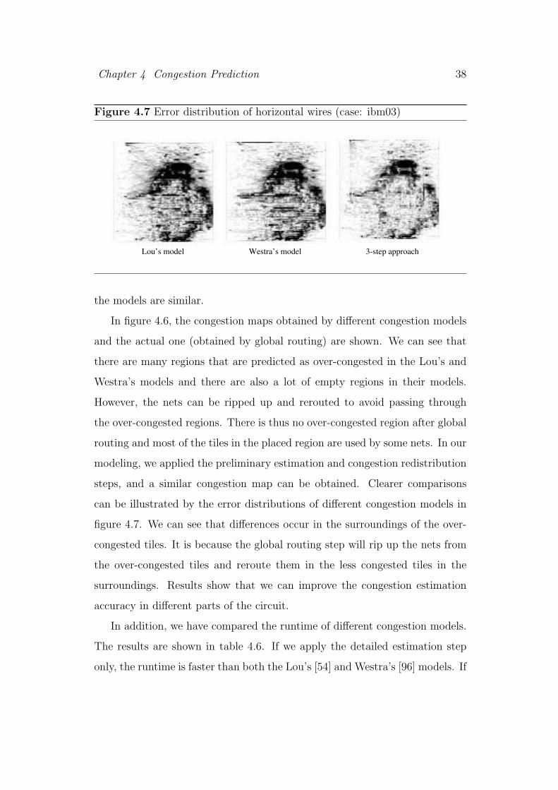
Figure 4.7 Error distribution of horizontal wires (case: ibm03)
Lou’s model Westra’s model 3-step approach
the models are similar.
In figure 4.6, the congestion maps obtained by different congestion models
and the actual one (obtained by global routing) are shown. We can see that
there are many regions that are predicted as over-congested in the Lou’s and
Westra’s models and there are also a lot of empty regions in their models.
However, the nets can be ripped up and rerouted to avoid passing through
the over-congested regions. There is thus no over-congested region after global
routing and most of the tiles in the placed region are used by some nets. In our
modeling, we applied the preliminary estimation and congestion redistribution
steps, and a similar congestion map can be obtained. Clearer comparisons
can be illustrated by the error distributions of different congestion models in
figure 4.7. We can see that differences occur in the surroundings of the over-
congested tiles. It is because the global routing step will rip up the nets from
the over-congested tiles and reroute them in the less congested tiles in the
surroundings. Results show that we can improve the congestion estimation
accuracy in different parts of the circuit.
In addition, we have compared the runtime of different congestion models.
The results are shown in table 4.6. If we apply the detailed estimation step
only, the runtime is faster than both the Lou’s [54] and Westra’s [96] models. If
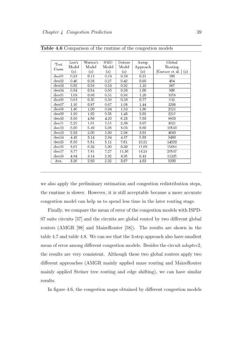
Chapter 4 Congestion Prediction 39
Table 4.6 Comparison of the runtime of the congestion models
we also apply the preliminary estimation and congestion redistribution steps,
the runtime is slower. However, it is still acceptable because a more accurate
congestion model can help us to spend less time in the later routing stage.
Finally, we compare the mean of error of the congestion models with ISPD-
07 suite circuits [37] and the circuits are global routed by two different global
routers (AMGR [98] and MaizeRouter [58]). The results are shown in the
table 4.7 and table 4.8. We can see that the 3-step approach also have smallest
mean of error among different congestion models. Besides the circuit adaptec2,
the results are very consistent. Although these two global routers apply two
different approaches (AMGR mainly applied maze routing and MaizeRouter
mainly applied Steiner tree routing and edge shifting), we can have similar
results.
In figure 4.6, the congestion maps obtained by different congestion models

Chapter 4 Congestion Prediction 40
Table 4.7 Comparison on the mean of error of the congestion models whenthe circuit is global routed by AMGR
Table 4.8 Comparison on the mean of error of the congestion models whenthe circuit is global routed by MaizeRouter
and the actual one (obtained by global routing) are shown. We can see that
there are many regions that are predicted as over-congested in the Lou’s and
Westra’s models and there are also a lot of empty regions in their models.
However, the nets can be ripped up and rerouted to avoid passing through
the over-congested regions. There is thus no over-congested region after global
routing and most of the tiles in the placed region are more or less used by some
nets. In our modeling, we applied the preliminary estimation and congestion
redistribution steps, and a similar congestion map can be obtained compared
with the routing map. From these subjective results, we can conclude that our

Chapter 4 Congestion Prediction 41
model is more accurate than the other two.
4.8 Summary
In this chapter we analyze three models of congestion prediction in the early
stages of VLSI physical design. SMD model is the fastest technique with
the least amount of calculation involved. Detour model pays attention to
surrounding tiles and 3-step approach with congestion redistribution is proved
to be the most accurate one. Apparently, from the performance comparison we
can conclude that our models have made significant improvement on accuracy
of prediction compared to the previous models.
Chapter 5
Clock Network Synthesis
5.1 Overview
In this chapter, we propose two novel clock network synthesizers, DMST and
DMSTSS. Some heuristics are proposed to optimize the CLR as well as the
clock skew and the power usage. It mainly contains the following features:
(1) A dual-MST based perfect matching algorithm is developed for symmetric
clock tree construction. (2) A look-up table based hierarchical buffer sizing
approach is developed for variation tolerance improvement. (3) An iterative
buffer insertion technique is developed for delay balancing and capacitance
reduction. (4) A dual-MZ blockage handling technique is developed for buffer
location distribution and blockage avoidance. SPICE simulation is also applied
for accurate delay estimation, the internal nodes of the clock tree are thus relo-
cated for further skew minimization. A slew constraint (≤ 100ps) is employed
in our synthesizer. We build a slew table for real-time reference during the
execution of our program to satisfy this constraint.
In addition to the measurement of CLR, Monte Carlo simulation is also
applied in the experiments. Monte Carlo simulation can simulate the variation
of buffers, so as to provide a common method for performance evaluation of
our clock network synthesizer. It can ensure that our proposed approach is
practically variation-tolerant.
42

Chapter 5 Clock Network Synthesis 43
5.2 Problem Formulation
Let T = V,E denote the clock tree. V = vi|i = 1, 2, . . . ,mv is the set of
nodes, and E = ej|j = 1, 2, . . . ,mv − 1 is the set of clock edges between the
node vj and its corresponding parent. Let |ej| denote the length of the edge
ej. We use S = vk|k = 1, 2, . . . ,ms (where ms < mv) to denote the set of
modules (the sinks, or leaf nodes). dsidenotes the signal delay of the ith sink.
The rest (mv − ms) nodes are named internal nodes. We use |V |, |E| and |S|
to indicate the number of elements in V , E and S, respectively. The leaves
are at level 0, and the root is at the highest level. Node vi is said to be at
level ni if there are ni edges on the path from vi to the farthest leaf of the tree.
Moreover, we assume that the topology of the clock tree is full binary, and
every internal node has exactly two children. The skew of T is the difference
between the longest signal delay and the shortest signal delay from the source
to any sinks. Detailed definition can be found in the ISPD 2009 contest [88].
The restriction on clock slew describes the requirement on the signal tran-
sition time reduction. It is defined to be the rising time from 10% to 90%
of the signal strength (90% to 10% for the falling time, respectively). The
upper limit is set to be 100ps. During the clock tree synthesis, it is necessary
to maintain the signal transition time under this upper limit throughout the
whole network.
CLR is the major metric in the performance evaluation. Two independent
SPICE simulations under different voltage source (Vdd1or Vdd2
) are applied.
The value of CLR is determined by the difference between the maximal and
minimal clock skew values under the two given voltage sources. Meanwhile,
nominal clock skew is also considered, which is the maximal clock skew of all
the voltage settings.
The power consumed by CMOS circuits consists of two components: static
and dynamic power. The static power is mostly determined by the feature size
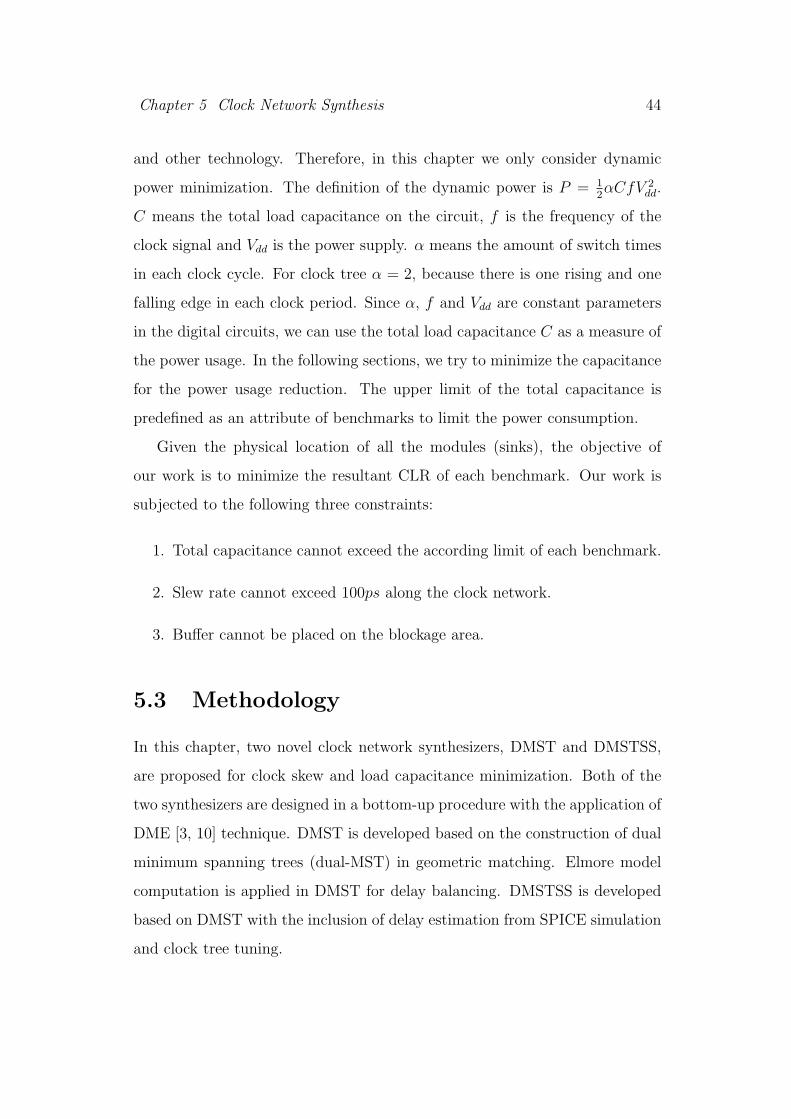
Chapter 5 Clock Network Synthesis 44
and other technology. Therefore, in this chapter we only consider dynamic
power minimization. The definition of the dynamic power is P = 12αCfV 2
dd.
C means the total load capacitance on the circuit, f is the frequency of the
clock signal and Vdd is the power supply. α means the amount of switch times
in each clock cycle. For clock tree α = 2, because there is one rising and one
falling edge in each clock period. Since α, f and Vdd are constant parameters
in the digital circuits, we can use the total load capacitance C as a measure of
the power usage. In the following sections, we try to minimize the capacitance
for the power usage reduction. The upper limit of the total capacitance is
predefined as an attribute of benchmarks to limit the power consumption.
Given the physical location of all the modules (sinks), the objective of
our work is to minimize the resultant CLR of each benchmark. Our work is
subjected to the following three constraints:
1. Total capacitance cannot exceed the according limit of each benchmark.
2. Slew rate cannot exceed 100ps along the clock network.
3. Buffer cannot be placed on the blockage area.
5.3 Methodology
In this chapter, two novel clock network synthesizers, DMST and DMSTSS,
are proposed for clock skew and load capacitance minimization. Both of the
two synthesizers are designed in a bottom-up procedure with the application of
DME [3, 10] technique. DMST is developed based on the construction of dual
minimum spanning trees (dual-MST) in geometric matching. Elmore model
computation is applied in DMST for delay balancing. DMSTSS is developed
based on DMST with the inclusion of delay estimation from SPICE simulation
and clock tree tuning.
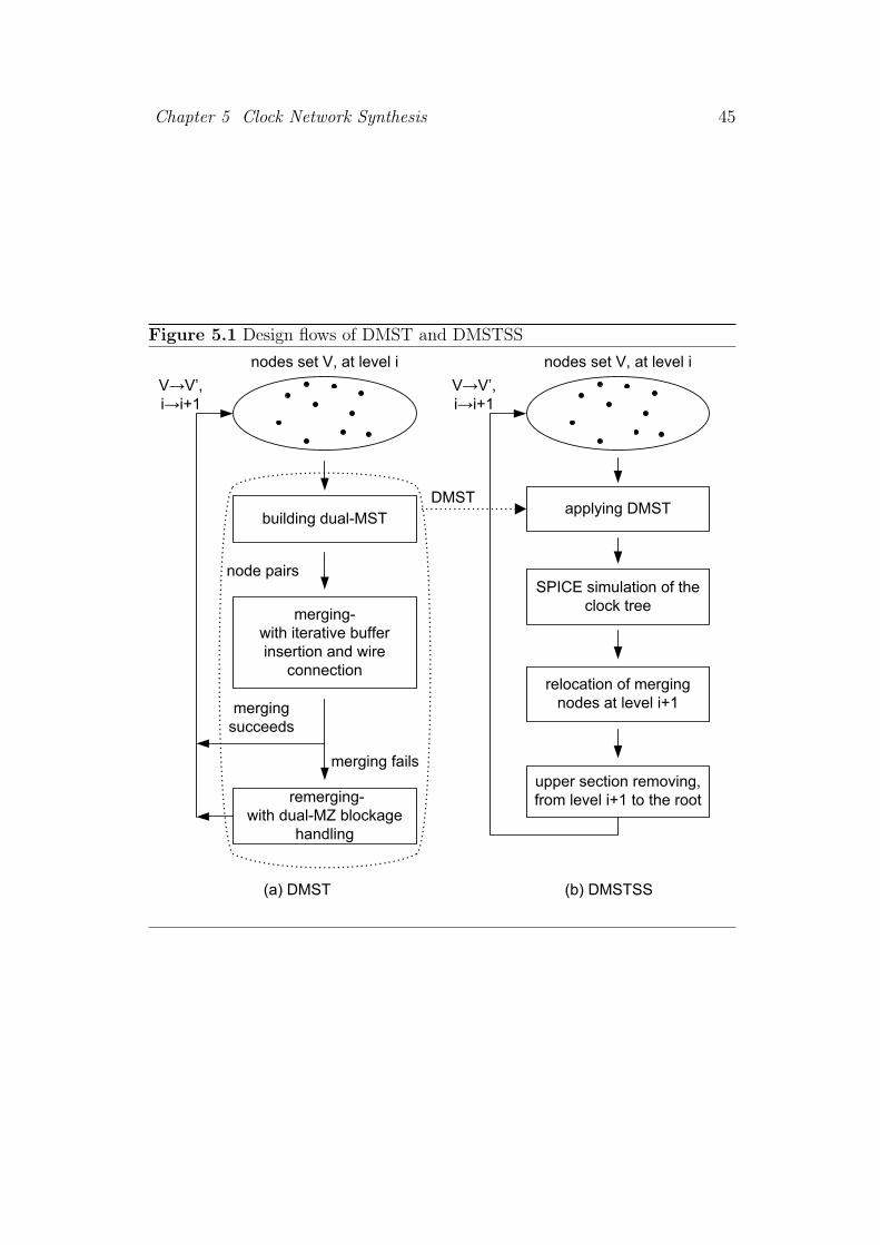
Chapter 5 Clock Network Synthesis 45
Figure 5.1 Design flows of DMST and DMSTSS
nodes set V, at level i
building dual-MST
merging-
with iterative buffer
insertion and wire
connection
merging
succeeds
remerging-
with dual-MZ blockage
handling
relocation of merging
nodes at level i+1
(a) DMST
applying DMST
(b) DMSTSS
SPICE simulation of the
clock tree
merging fails
nodes set V, at level i
V V’,
i i+1
node pairs
upper section removing,
from level i+1 to the root
V V’,
i i+1
DMST

Chapter 5 Clock Network Synthesis 46
DMST is an iterative approach, the general procedure of DMST is shown
in figure 5.1(a). At the beginning of each iteration, we have a group of nodes
to be merged. This is denoted as V . V can be composed of either clock sinks
or internal nodes. A dual-MST based perfect matching technique is applied
first to obtain a geometric matching solution upon the node group V . During
the merging of each matched pair of nodes, a new technique of iterative buffer
insertion and wire connection is applied to deal with the buffer distribution
problem. If the merging fails because of blockages, this pair is re-merged
with an exclusive dual-MZ blockage handling technique. After the successful
merging of all the nodes in V and the generation of the nodes in V ′, this
procedure is finished. It is then performed iteratively with V replaced by V ′,
until a complete clock tree is constructed.
DMSTSS is a more advanced synthesizer. It is developed based on DMST
with real-time SPICE simulation included for delay estimation. The flow of
DMSTSS and its relationship with DMST are illustrated in figure 5.1(b). A
clock tree is firstly built up by employing DMST. Then SPICE simulation is
applied and the whole clock tree is specified with detailed signal delay infor-
mation. Based on this, the internal nodes of each level are relocated for clock
skew minimization. Notice that the synthesis result of DMSTSS is no longer a
zero skew tree in terms of the Elmore model, but it has better performance in
real circuits work. The details of our techniques are discussed in the following
parts.
5.3.1 A Dual-MST based Geometric Perfect Matching
Traditional matching algorithms mainly focused on wirelength minimization [40,
24]. Our approach focuses on the construction of symmetric topology. In our
clock tree, every root-to-leaf path will have similar buffer and wire distri-
bution. This design will make the clock tree less sensitive towards process
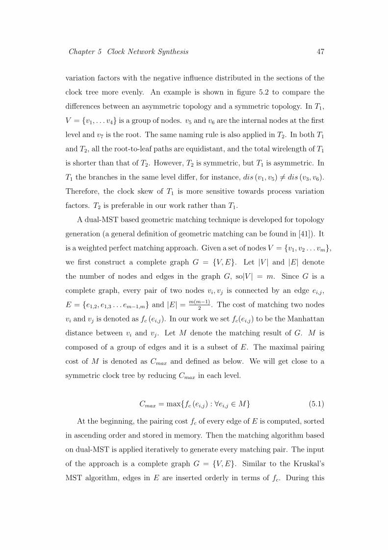
Chapter 5 Clock Network Synthesis 47
variation factors with the negative influence distributed in the sections of the
clock tree more evenly. An example is shown in figure 5.2 to compare the
differences between an asymmetric topology and a symmetric topology. In T1,
V = v1, . . . v4 is a group of nodes. v5 and v6 are the internal nodes at the first
level and v7 is the root. The same naming rule is also applied in T2. In both T1
and T2, all the root-to-leaf paths are equidistant, and the total wirelength of T1
is shorter than that of T2. However, T2 is symmetric, but T1 is asymmetric. In
T1 the branches in the same level differ, for instance, dis (v1, v5) 6= dis (v3, v6).
Therefore, the clock skew of T1 is more sensitive towards process variation
factors. T2 is preferable in our work rather than T1.
A dual-MST based geometric matching technique is developed for topology
generation (a general definition of geometric matching can be found in [41]). It
is a weighted perfect matching approach. Given a set of nodes V = v1, v2 . . . vm,
we first construct a complete graph G = V,E. Let |V | and |E| denote
the number of nodes and edges in the graph G, so|V | = m. Since G is a
complete graph, every pair of two nodes vi, vj is connected by an edge ei,j,
E = e1,2, e1,3 . . . em−1,m and |E| = m(m−1)2
. The cost of matching two nodes
vi and vj is denoted as fc (ei,j). In our work we set fc(ei,j) to be the Manhattan
distance between vi and vj. Let M denote the matching result of G. M is
composed of a group of edges and it is a subset of E. The maximal pairing
cost of M is denoted as Cmax and defined as below. We will get close to a
symmetric clock tree by reducing Cmax in each level.
Cmax = maxfc (ei,j) : ∀ei,j ∈ M (5.1)
At the beginning, the pairing cost fc of every edge of E is computed, sorted
in ascending order and stored in memory. Then the matching algorithm based
on dual-MST is applied iteratively to generate every matching pair. The input
of the approach is a complete graph G = V,E. Similar to the Kruskal’s
MST algorithm, edges in E are inserted orderly in terms of fc. During this
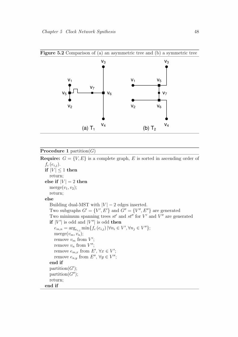
Chapter 5 Clock Network Synthesis 48
Figure 5.2 Comparison of (a) an asymmetric tree and (b) a symmetric tree
(a) T1 (b) T2
v5
v3
v1
v2
v4
v6
v7
v1
v2
v3
v4
v7
v5
v6
Procedure 1 partition(G)
Require: G = V,E is a complete graph, E is sorted in ascending order offc (ei,j).if |V | ≤ 1 then
return;else if |V | = 2 then
merge(v1, v2);return;
elseBuilding dual-MST with |V | − 2 edges inserted.Two subgraphs G′ = V ′, E ′ and G′′ = V ′′, E ′′ are generatedTwo minimum spanning trees st′ and st′′ for V ′ and V ′′ are generatedif |V ′| is odd and |V ′′| is odd then
em,n = argei,jminfc (ei,j) |∀ni ∈ V ′,∀nj ∈ V ′′;
merge(vm, vn);remove vm from V ′;remove vn from V ′′;remove em,x from E ′, ∀x ∈ V ′;remove en,y from E ′′, ∀y ∈ V ′′;
end ifpartition(G′);partition(G′′);return;
end if
Chapter 5 Clock Network Synthesis 49
procedure, no cycle is allowed. When |V | − 2 edges have been inserted, two
disjoint sub-trees st′ and st′′ are generated. Meanwhile, G is divided into two
disjoint complete sub-graphs G′ = V ′, E ′ and G′′ = V ′′, E ′′. Notice that
all the nodes of V ′ are connected by st′, and all the nodes of V ′′ are connected
by st′′, respectively. It is obvious that st′ and st′′ are two minimum spanning
trees for G′ and G′′, so dual-MST have been built up. If either |V ′| or |V ′′| is
an even number, it goes to the next iteration. Otherwise, an edge subset E0
will be extracted from E. Every edge ei,j of E0 has one node vi from V ′ and
the other node vj from V ′′. The edge em,n of E0 with the minimum cost value
fc is determined as a matching pair.
fc (em,n) = minfc (ei,j) : ∀ei,j ∈ E0 (5.2)
Notice that this dual-MST based matching approach is a geometric perfect
matching. This means 2×⌊ |V |2⌋ nodes will be matched, and ⌈log2 |S|⌉ levels are
performed. Assume that we are at the ith level with the node group Vi. The
time complexity of fc computation equals O(
|Vi|2). On average, the number
of partitioning stages is ⌈log2 (|Vi|)⌉. Thus the time complexity of partitioning
is calculated as below.
O
⌈log2(|Vi|)⌉∑
j=1
(
1
2×
|Vi|
2j−1×
(
|Vi|
2j−1− 1
)
× 2j−1
)
(5.3)
Therefore, the total complexity of the ith level is still O(|Vi|2) on average.
While |Vi| = ⌈ |S|2i−1 ⌉, the time complexity on average for the whole geometric
matching is shown below.
O
⌈log2 |S|⌉∑
i=1
⌈|S|
2i−1⌉2
= O(
|S|2)
(5.4)
Our approach aims at constructing a symmetric clock tree but it is only a
heuristic giving close proximity to the optimal solution. Compared to other
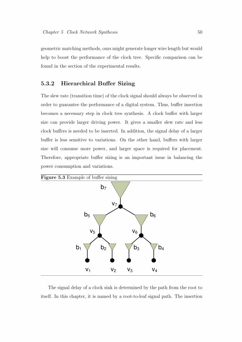
Chapter 5 Clock Network Synthesis 50
geometric matching methods, ours might generate longer wire length but would
help to boost the performance of the clock tree. Specific comparison can be
found in the section of the experimental results.
5.3.2 Hierarchical Buffer Sizing
The slew rate (transition time) of the clock signal should always be observed in
order to guarantee the performance of a digital system. Thus, buffer insertion
becomes a necessary step in clock tree synthesis. A clock buffer with larger
size can provide larger driving power. It gives a smaller slew rate and less
clock buffers is needed to be inserted. In addition, the signal delay of a larger
buffer is less sensitive to variations. On the other hand, buffers with larger
size will consume more power, and larger space is required for placement.
Therefore, appropriate buffer sizing is an important issue in balancing the
power consumption and variations.
Figure 5.3 Example of buffer sizing
v5 v6
v7
v1 v2 v3 v4
b7
b5 b6
b1 b2 b3 b4
The signal delay of a clock sink is determined by the path from the root to
itself. In this chapter, it is named by a root-to-leaf signal path. The insertion

Chapter 5 Clock Network Synthesis 51
point at a higher level will occupy a larger number of such root-to-leaf signal
paths. As shown in figure 5.3, v7 at level 2 will cover 4 downstream clock sinks
(v1, v2, v3, v4) and v5 at level 1 will cover 2 downstream clock sinks (v1, v2).
Therefore, we should enlarge the size of the buffers at higher levels to balance
the signal delay of more clock sinks. Ideally, the clock buffers can be sized
according to the example in figure 5.3. In this example, buffers with larger
size will be inserted in upper levels and the smaller buffers will be used in lower
level of the clock tree. In this chapter, an algorithm is devised to appropriately
design the buffer size in descending order from the root to the leaves. Given
one type of buffer, we connect a group of buffers in parallel to simulate larger
buffer sizes.
Our main target in clock tree synthesis is to minimize the negative effect
caused by variation factors. For this target, every root-to-leaf path should be
constructed in similar pattern, with proper buffer location and sizing. Thus
the number of buffer levels in each root-to-leaf path should be exactly the
same. Moreover, the size of the buffer insertion in each buffer level should also
be the same for all the sinks. Under this precondition, the size of the buffers
at each insertion point is uniquely determined by its downstream buffer levels.
It is a waste of time to devise the size for any specific insertion point during
the synthesis. We develop a sizing rule based on some internal attributes of
the clock sinks. During the procedure of clock tree synthesis, we compute the
optimal size for each buffer level in advance and build up a table for buffer
sizing reference. Subsequently, all the buffer insertion will follow this sizing
table to determine its buffer size.
Here, we describe our rule for the construction of buffer sizing table. We
define the total amount of different buffer sizes to be an integer m. Let szb (x)
denote the objective buffer size and x denote the amount of downstream buffer
levels. According to figure 5.3, szb (x) is a monotonically increasing function.
Moreover, we define L = L0, L1, . . . , Lm to be the buffer levels between
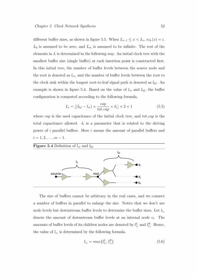
Chapter 5 Clock Network Synthesis 52
different buffer sizes, as shown in figure 5.5. When Li−1 ≤ x < Li, szb (x) = i.
L0 is assumed to be zero, and Lm is assumed to be infinite. The rest of the
elements in L is determined in the following way. An initial clock tree with the
smallest buffer size (single buffer) at each insertion point is constructed first.
In this initial tree, the number of buffer levels between the source node and
the root is denoted as lrt, and the number of buffer levels between the root to
the clock sink within the longest root-to-leaf signal path is denoted as lbf . An
example is shown in figure 5.4. Based on the value of lrt and lbf , the buffer
configuration is computed according to the following formula,
Li = ⌊(lbf − lrt) ×cap
tot cap× δi⌋ × 2 + 1 (5.5)
where cap is the used capacitance of the initial clock tree, and tot cap is the
total capacitance allowed. δi is a parameter that is related to the driving
power of i parallel buffers. Here i means the amount of parallel buffers and
i = 1, 2, . . . ,m − 1.
Figure 5.4 Definition of lrt and lbf
source
si
lrt
lbf
root
sk
sj
The size of buffers cannot be arbitrary in the real cases, and we connect
a number of buffers in parallel to enlarge the size. Notice that we don’t use
node levels but downstream buffer levels to determine the buffer sizes. Let lvi
denote the amount of downstream buffer levels at an internal node vi. The
amounts of buffer levels of its children nodes are denoted by lLviand lRvi
. Hence,
the value of lviis determined by the following formula.
lvi= maxlLvi
, lRvi (5.6)
Chapter 5 Clock Network Synthesis 53
Figure 5.5 A clock tree divided by buffer levels L1 and L2
L2 L1
lvi= 0 if vi is a sink node. Since it is a bottom-up method, the correspond-
ing buffer levels of the internal nodes can be computed in this way.
5.3.3 Iterative Buffer Insertion
In our synthesizer of DMST, the topology is constructed level by level with
concurrent buffer insertion and wire connection. This is mainly because ac-
curate sub-tree information is important at geometric matching in each level.
In DMSTSS, we will iteratively remove and rebuild the upper levels of the
clock tree for merging point tuning. Global buffer distribution in the whole
clock tree may lead to local cost increment for other tree sections. However,
these benefited tree sections may be removed in the further tuning. Thus, it is
improper to distribute the buffers globally along the whole tree. We developed
a greedy algorithm of iterative buffer insertion, which is mainly focus on local
optimization with skew balancing and load capacitance minimization.
An example is illustrated in figure 5.6 to demonstrate our approach for
merging two nodes v1 and v2. Let e1,2 denote the edge connecting the two
nodes. Based on their downstream capacitances and sub-tree delays, the lo-
cation of the delay balancing point, v0, can be computed. Let lv1denote
the amount of downstream buffer levels of v1, and lv2denote the amount of
downstream buffer levels of v2, respectively. Generally, our method of buffer
distribution can be divided into the following two parts.
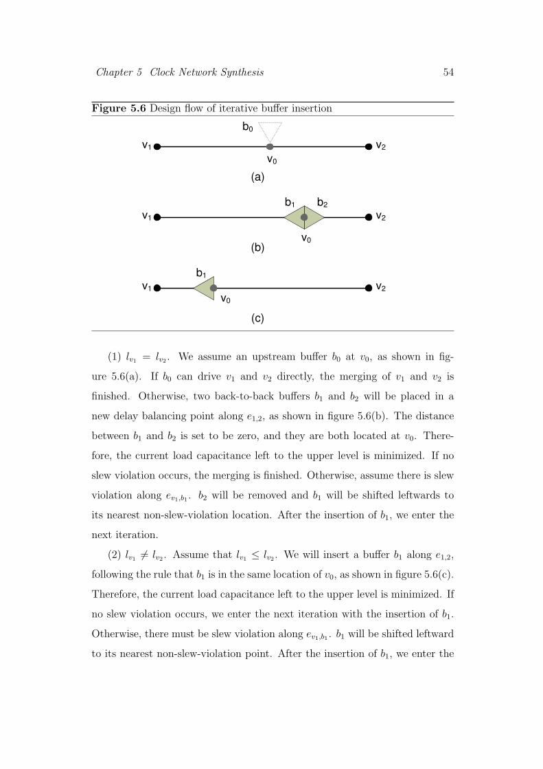
Chapter 5 Clock Network Synthesis 54
Figure 5.6 Design flow of iterative buffer insertion
(a)
(b)
(c)
v0
b1
v1 v2
b1
b0
v1 v2
b2
v0
v0
v2v1
(1) lv1= lv2
. We assume an upstream buffer b0 at v0, as shown in fig-
ure 5.6(a). If b0 can drive v1 and v2 directly, the merging of v1 and v2 is
finished. Otherwise, two back-to-back buffers b1 and b2 will be placed in a
new delay balancing point along e1,2, as shown in figure 5.6(b). The distance
between b1 and b2 is set to be zero, and they are both located at v0. There-
fore, the current load capacitance left to the upper level is minimized. If no
slew violation occurs, the merging is finished. Otherwise, assume there is slew
violation along ev1,b1 . b2 will be removed and b1 will be shifted leftwards to
its nearest non-slew-violation location. After the insertion of b1, we enter the
next iteration.
(2) lv16= lv2
. Assume that lv1≤ lv2
. We will insert a buffer b1 along e1,2,
following the rule that b1 is in the same location of v0, as shown in figure 5.6(c).
Therefore, the current load capacitance left to the upper level is minimized. If
no slew violation occurs, we enter the next iteration with the insertion of b1.
Otherwise, there must be slew violation along ev1,b1 . b1 will be shifted leftward
to its nearest non-slew-violation point. After the insertion of b1, we enter the

Chapter 5 Clock Network Synthesis 55
next iteration.
Notice that in the next iteration, v0 replaces v1 as an input node, and
v2 is remained. Similarly, e0,2 replaces e1,2. In our discussion of iterative
buffer insertion, only straight wire connection is described in details. However,
snaking cannot be completely avoided in some particular cases. When the
delay difference between the two nodes cannot be solved with straight wire
balancing, snaking wire technique can be applied.
5.3.4 Dual-MZ Blockage Handling Technique
Because of the existence of macro blocks, there may be pre-assigned obstacles
on the chip area. Wires can cover these blockage areas freely, but buffers
will cause violation. The connection is thus constrained. Traditionally, clock
tree synthesizer can be divided into two steps. They do clock routing first to
connect all the sinks to the signal source. Subsequently, buffer sizing, insertion
and wire sizing are determined then. In case of buffer violation in the second
step, clock routing has to detour out of the blockage areas in the first step. An
example of possible result of traditional synthesis is shown in figure 5.8(a).
Instead of above mentioned approach, our approach considers concurrent
buffer sizing and insertion during the procedure of clock routing. A novel
blockage handling method, dual-MZ, is developed based on the traditional
maze routing technique. Several enhancements are developed to make it satisfy
the clock network synthesis constraints. We first decompose the chip into a
M × N grid. Assume that v1 and v2 are the two nodes to be merged. Two
independent maze routers mz1 and mz2 are initialized for v1 and v2, exclusively.
Therefore, a dual-MZ is constructed. The priority queue of each maze router
is sorted by the downstream delay values of its elements in ascending orders.
Let dly1 and dly2 denote the minimum downstream delays of mz1 and mz2.
Without loss of generality, assume that dly1 ≤ dly2, and mz1 is selected to be

Chapter 5 Clock Network Synthesis 56
the primary router. Like ordinary maze routing, it will search the four adjacent
grid points in one iteration. The downstream delay of mz1 is then increased,
so dly1 will be updated. When dly1 becomes bigger than dly2, mz2 will replace
mz1 to be the primary router and continue the routing job. In this way, mz1
and mz2 are executed in turns, and the values of dly1 and dly2 stay close to
each other. A design flow of dual-MZ is shown in figure 5.7. When the two
routers meet at the end, their accumulated delays will not differ a lot. dual-MZ
can result in less buffer insertions and wire detours, so the power consumption
is reduced. Notice that during this procedure, wire connection together with
buffer insertion is concurrently applied along the propagation trace of the two
routers, and they both contribute to the delay accumulation for comparison.
A possible synthesis result of dual-MZ is shown in figure 5.8(b).
Our dual-MZ can save resources with less buffers and wires cost involved.
Notice that the size of the grid graph (M × N) is manually determined in
our algorithm. M and N can be scaled in order to derive a tradeoff between
routing complexity and routing quality. In our experiments, both M and
N are set to be 1000. A synthesis result of the benchmark ispd09fnb1 is
shown in figure 5.9 (the detailed information of ispd09fnb1 can be found in
table 5.2). The green stars denote the clock sinks, the blue squares denote the
buffers, the purple circle denotes the signal source, the red lines denote the
wire connection and the gray rectangles denote the blockage areas. We can see
that by applying dual-MZ, clock wire can cover the blockage area freely with
proper buffer insertion outside. Resources cost can be reduced by our method
efficiently.
5.3.5 Merging Point Relocation with SPICE Simulation
DMSTSS is an advanced version of DMST with SPICE tuning involved. Given
a clock tree, SPICE simulation can provide accurate delay estimation at any
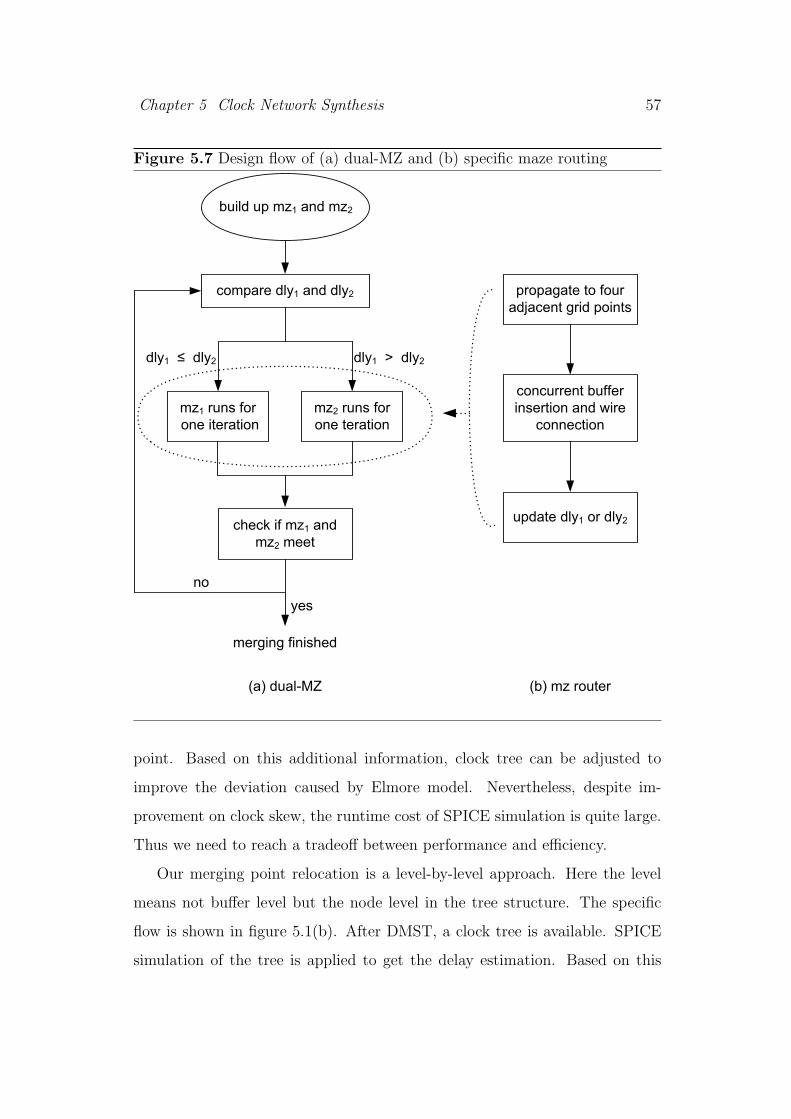
Chapter 5 Clock Network Synthesis 57
Figure 5.7 Design flow of (a) dual-MZ and (b) specific maze routing
compare dly1 and dly2
concurrent buffer
insertion and wire
connection
update dly1 or dly2
(a) dual-MZ
propagate to four
adjacent grid points
(b) mz router
mz1 runs for
one iteration
dly1 dly2 dly1 > dly2
mz2 runs for
one teration
check if mz1 and
mz2 meet
yes
no
build up mz1 and mz2
merging finished
point. Based on this additional information, clock tree can be adjusted to
improve the deviation caused by Elmore model. Nevertheless, despite im-
provement on clock skew, the runtime cost of SPICE simulation is quite large.
Thus we need to reach a tradeoff between performance and efficiency.
Our merging point relocation is a level-by-level approach. Here the level
means not buffer level but the node level in the tree structure. The specific
flow is shown in figure 5.1(b). After DMST, a clock tree is available. SPICE
simulation of the tree is applied to get the delay estimation. Based on this
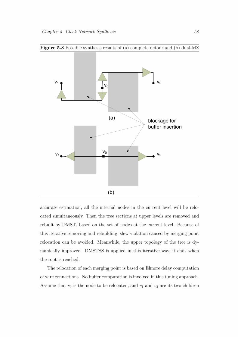
Chapter 5 Clock Network Synthesis 58
Figure 5.8 Possible synthesis results of (a) complete detour and (b) dual-MZ
0
01 2
1 2
accurate estimation, all the internal nodes in the current level will be relo-
cated simultaneously. Then the tree sections at upper levels are removed and
rebuilt by DMST, based on the set of nodes at the current level. Because of
this iterative removing and rebuilding, slew violation caused by merging point
relocation can be avoided. Meanwhile, the upper topology of the tree is dy-
namically improved. DMSTSS is applied in this iterative way, it ends when
the root is reached.
The relocation of each merging point is based on Elmore delay computation
of wire connections. No buffer computation is involved in this tuning approach.
Assume that v0 is the node to be relocated, and v1 and v2 are its two children
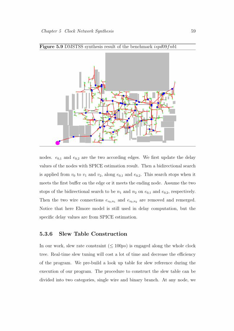
Chapter 5 Clock Network Synthesis 59
Figure 5.9 DMSTSS synthesis result of the benchmark ispd09fnb1
nodes. e0,1 and e0,2 are the two according edges. We first update the delay
values of the nodes with SPICE estimation result. Then a bidirectional search
is applied from v0 to v1 and v2, along e0,1 and e0,2. This search stops when it
meets the first buffer on the edge or it meets the ending node. Assume the two
stops of the bidirectional search to be n1 and n2 on e0,1 and e0,2, respectively.
Then the two wire connections ev0,n1and ev0,n2
are removed and remerged.
Notice that here Elmore model is still used in delay computation, but the
specific delay values are from SPICE estimation.
5.3.6 Slew Table Construction
In our work, slew rate constraint (≤ 100ps) is engaged along the whole clock
tree. Real-time slew tuning will cost a lot of time and decrease the efficiency
of the program. We pre-build a look up table for slew reference during the
execution of our program. The procedure to construct the slew table can be
divided into two categories, single wire and binary branch. At any node, we

Chapter 5 Clock Network Synthesis 60
need to get the maximum driving length from the slew table, with upstream
buffer size, downstream buffer size and downstream wirelength as the indexes.
This is shown in figure 5.10. We can assume that the current node to be v0,
and l0 is the maximum driving length for the next buffer insertion b0. l0 is what
we need to get from the slew table in the program. As shown in figure 5.5, the
buffer size szb0 for the next level can be derived from our buffer sizing table, so
it is a know value. At the single wire in figure 5.10(a), downstream information
of szb1 and l1 are ready to utilize. Therefore, with three available indexes of
szb0 , szb1 and l1, we can get l0 from the slew table. We can get l0 for a binary
branch in the same way, as shown in figure 5.10(b). The only difference is that
there are two additional indexes required for the slew table, which are szb2 and
l2 as the downstream buffer size and wire length of the other branch.
As stated in 5.3.2, buffer size are defined by the number of parallel buffer
connection in our work. Thus szb0 , szb1 and szb2 are discrete values (integers
actually) and they can be used as table indexes directly. However, wire length
is a real continuous value in nanometer scale. Therefore, we quantize the wire
length of l0, l1 and l2 during the slew table construction in order to maintain
the table size within a proper range. During the clock tree synthesis, a linear
interpolation program is applied to transfer the actual wire length into discrete
table index.
Figure 5.10 Driving length reference at (a) single wire and (b) binary branch
(a) (b)
b1
l1
b0
l0
b1
l1
b0
l0
b2
l2
v0 v0
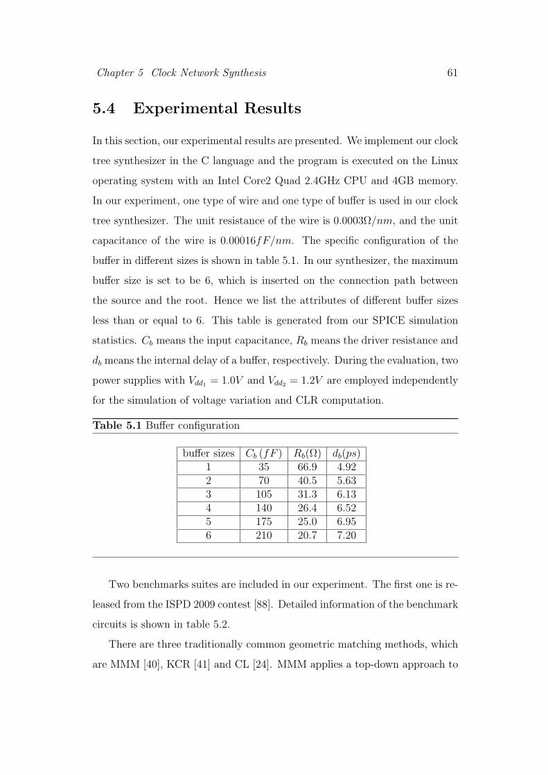
Chapter 5 Clock Network Synthesis 61
5.4 Experimental Results
In this section, our experimental results are presented. We implement our clock
tree synthesizer in the C language and the program is executed on the Linux
operating system with an Intel Core2 Quad 2.4GHz CPU and 4GB memory.
In our experiment, one type of wire and one type of buffer is used in our clock
tree synthesizer. The unit resistance of the wire is 0.0003Ω/nm, and the unit
capacitance of the wire is 0.00016fF/nm. The specific configuration of the
buffer in different sizes is shown in table 5.1. In our synthesizer, the maximum
buffer size is set to be 6, which is inserted on the connection path between
the source and the root. Hence we list the attributes of different buffer sizes
less than or equal to 6. This table is generated from our SPICE simulation
statistics. Cb means the input capacitance, Rb means the driver resistance and
db means the internal delay of a buffer, respectively. During the evaluation, two
power supplies with Vdd1= 1.0V and Vdd2
= 1.2V are employed independently
for the simulation of voltage variation and CLR computation.
Table 5.1 Buffer configuration
buffer sizes Cb (fF ) Rb(Ω) db(ps)1 35 66.9 4.922 70 40.5 5.633 105 31.3 6.134 140 26.4 6.525 175 25.0 6.956 210 20.7 7.20
Two benchmarks suites are included in our experiment. The first one is re-
leased from the ISPD 2009 contest [88]. Detailed information of the benchmark
circuits is shown in table 5.2.
There are three traditionally common geometric matching methods, which
are MMM [40], KCR [41] and CL [24]. MMM applies a top-down approach to
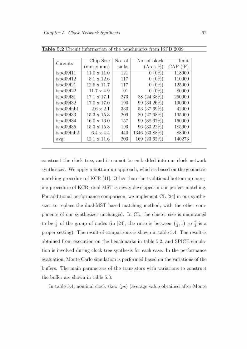
Chapter 5 Clock Network Synthesis 62
Table 5.2 Circuit information of the benchmarks from ISPD 2009
Chip Size No. of No. of block limitCircuits
(mm x mm) sinks (Area %) CAP (fF)ispd09f11 11.0 x 11.0 121 0 (0%) 118000ispd09f12 8.1 x 12.6 117 0 (0%) 110000ispd09f21 12.6 x 11.7 117 0 (0%) 125000ispd09f22 11.7 x 4.9 91 0 (0%) 80000ispd09f31 17.1 x 17.1 273 88 (24.38%) 250000ispd09f32 17.0 x 17.0 190 99 (34.26%) 190000ispd09fnb1 2.6 x 2.1 330 53 (37.69%) 42000ispd09f33 15.3 x 15.3 209 80 (27.68%) 195000ispd09f34 16.0 x 16.0 157 99 (38.67%) 160000ispd09f35 15.3 x 15.3 193 96 (33.22%) 185000ispd09fnb2 6.4 x 4.4 440 1346 (63.88%) 88000avg. 12.1 x 11.6 203 169 (23.62%) 140273
construct the clock tree, and it cannot be embedded into our clock network
synthesizer. We apply a bottom-up approach, which is based on the geometric
matching procedure of KCR [41]. Other than the traditional bottom-up merg-
ing procedure of KCR, dual-MST is newly developed in our perfect matching.
For additional performance comparison, we implement CL [24] in our synthe-
sizer to replace the dual-MST based matching method, with the other com-
ponents of our synthesizer unchanged. In CL, the cluster size is maintained
to be 23
of the group of nodes (in [24], the ratio is between(
12, 1
)
so 23
is a
proper setting). The result of comparisons is shown in table 5.4. The result is
obtained from execution on the benchmarks in table 5.2, and SPICE simula-
tion is involved during clock tree synthesis for each case. In the performance
evaluation, Monte Carlo simulation is performed based on the variations of the
buffers. The main parameters of the transistors with variations to construct
the buffer are shown in table 5.3.
In table 5.4, nominal clock skew (ps) (average value obtained after Monte
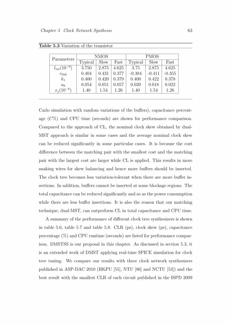
Chapter 5 Clock Network Synthesis 63
Table 5.3 Variation of the transistor
NMOS PMOSParameters
Typical Slow Fast Typical Slow Fastlint(10−9) 3.750 2.875 4.625 3.75 2.875 4.625
vth0 0.404 0.431 0.377 -0.384 -0.411 -0.355k1 0.400 0.420 0.379 0.400 0.422 0.378u0 0.054 0.051 0.057 0.020 0.018 0.022
xj(10−8) 1.40 1.54 1.26 1.40 1.54 1.26
Carlo simulation with random variations of the buffers), capacitance percent-
age (C%) and CPU time (seconds) are shown for performance comparison.
Compared to the approach of CL, the nominal clock skew obtained by dual-
MST approach is similar in some cases and the average nominal clock skew
can be reduced significantly in some particular cases. It is because the cost
difference between the matching pair with the smallest cost and the matching
pair with the largest cost are larger while CL is applied. This results in more
snaking wires for skew balancing and hence more buffers should be inserted.
The clock tree becomes less variation-tolerant when there are more buffer in-
sertions. In addition, buffers cannot be inserted at some blockage regions. The
total capacitance can be reduced significantly and so as the power consumption
while there are less buffer insertions. It is also the reason that our matching
technique, dual-MST, can outperform CL in total capacitance and CPU time.
A summary of the performance of different clock tree synthesizers is shown
in table 5.6, table 5.7 and table 5.8. CLR (ps), clock skew (ps), capacitance
percentage (%) and CPU runtime (seconds) are listed for performance compar-
ison. DMSTSS is our proposal in this chapter. As discussed in section 5.3, it
is an extended work of DMST applying real-time SPICE simulation for clock
tree tuning. We compare our results with three clock network synthesizers
published in ASP-DAC 2010 (HKPU [55], NTU [86] and NCTU [53]) and the
best result with the smallest CLR of each circuit published in the ISPD 2009
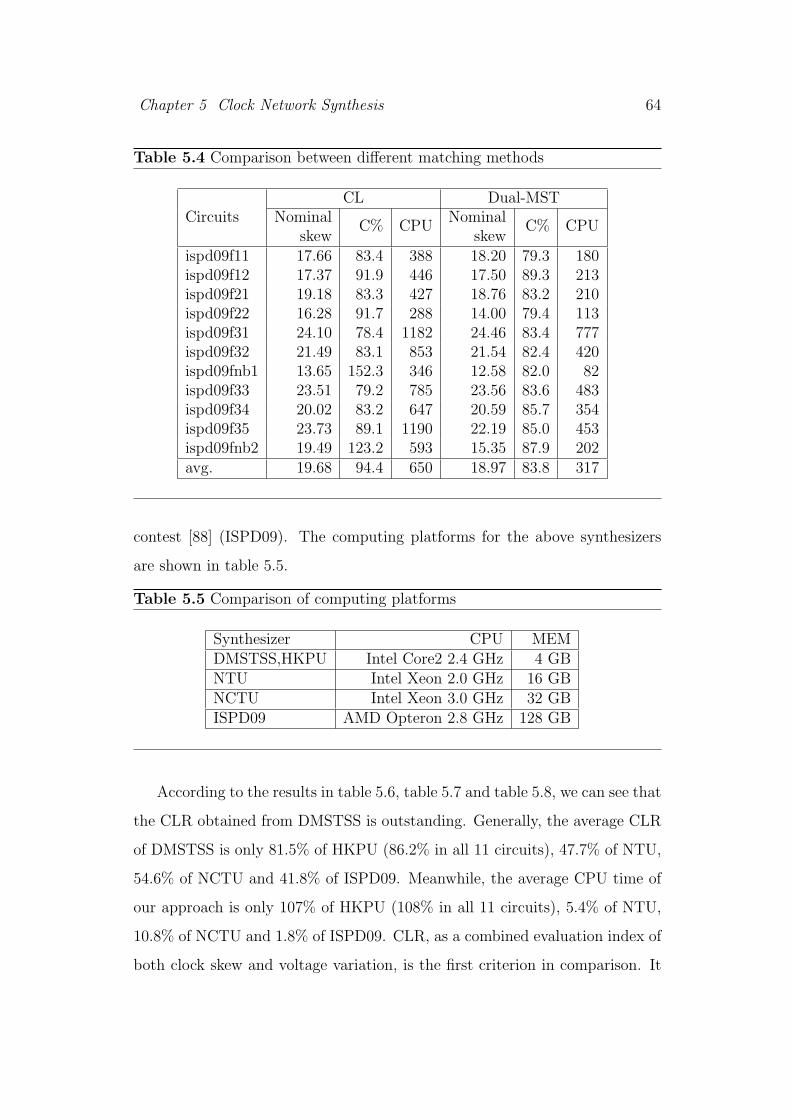
Chapter 5 Clock Network Synthesis 64
Table 5.4 Comparison between different matching methods
CL Dual-MSTCircuits Nominal Nominal
skewC% CPU
skewC% CPU
ispd09f11 17.66 83.4 388 18.20 79.3 180ispd09f12 17.37 91.9 446 17.50 89.3 213ispd09f21 19.18 83.3 427 18.76 83.2 210ispd09f22 16.28 91.7 288 14.00 79.4 113ispd09f31 24.10 78.4 1182 24.46 83.4 777ispd09f32 21.49 83.1 853 21.54 82.4 420ispd09fnb1 13.65 152.3 346 12.58 82.0 82ispd09f33 23.51 79.2 785 23.56 83.6 483ispd09f34 20.02 83.2 647 20.59 85.7 354ispd09f35 23.73 89.1 1190 22.19 85.0 453ispd09fnb2 19.49 123.2 593 15.35 87.9 202avg. 19.68 94.4 650 18.97 83.8 317
contest [88] (ISPD09). The computing platforms for the above synthesizers
are shown in table 5.5.
Table 5.5 Comparison of computing platforms
Synthesizer CPU MEMDMSTSS,HKPU Intel Core2 2.4 GHz 4 GBNTU Intel Xeon 2.0 GHz 16 GBNCTU Intel Xeon 3.0 GHz 32 GBISPD09 AMD Opteron 2.8 GHz 128 GB
According to the results in table 5.6, table 5.7 and table 5.8, we can see that
the CLR obtained from DMSTSS is outstanding. Generally, the average CLR
of DMSTSS is only 81.5% of HKPU (86.2% in all 11 circuits), 47.7% of NTU,
54.6% of NCTU and 41.8% of ISPD09. Meanwhile, the average CPU time of
our approach is only 107% of HKPU (108% in all 11 circuits), 5.4% of NTU,
10.8% of NCTU and 1.8% of ISPD09. CLR, as a combined evaluation index of
both clock skew and voltage variation, is the first criterion in comparison. It
Chapter 5 Clock Network Synthesis 65
Table 5.6 Comparison among DMSTSS, the three synthesizers in ASP-DAC2010 and the best result in ISPD 2009.
DMSTSS HKPU [55]Circuits
CLR SKEW C% CPU CLR SKEW C% CPUispd09f11 10.1 5.5 87.4 208 12.2 6.5 79.3 180ispd09f12 8.8 5.4 93.2 227 10.9 7.0 89.3 213ispd09f21 9.7 6.3 93.9 258 12.1 6.7 83.2 210ispd09f22 6.9 4.2 89.2 136 9.9 4.3 79.4 113ispd09f31 11.0 8.0 83.4 727 13.4 10.1 83.4 777ispd09f32 9.9 7.6 85.2 485 11.5 8.8 82.4 420ispd09fnb1 12.1 6.2 91.6 95 13.8 7.8 82.0 82avg.(7) 9.8 6.2 89.8 305 12.0 7.3 82.7 285ispd09f33 13.6 10.2 88.8 531 13.4 7.9 83.6 483ispd09f34 9.9 8.5 91.0 385 11.3 6.2 85.7 354ispd09f35 11.3 9.9 90.8 507 13.1 11.1 85.0 453ispd09fnb2 13.1 8.7 87.9 202 13.1 8.7 87.9 202avg.(11) 10.6 7.3 89.7 342 12.3 7.7 83.8 317
can be seen that our DMSTSS has great advantage on CLR compared to NTU,
NCTU and ISPD09. Even compared with our previous work HKPU, there
is still more than 10% improvement. Meanwhile, our synthesizer DMSTSS
is much faster than the proposed works. It is a little slower than that of
HKPU with less than 10% additional runtime, but the total efficiency is still
good. Additionally, due to the practicality problems of CLR (voltage supplies
at different points will not vary simultaneously), we listed the nominal clock
skew of each work as the SKEW (ps) in the tables. Notice that the clock skew
of DMSTSS is improved based on HKPU, although it is still larger than the
results of NTU, NCTU and ISPD09.
A summary of the performance of our clock tree synthesizer with fixed
buffer sizes is shown in table 5.9 and table 5.10. No buffer sizing technique is
applied here. CLR, capacitance percentage and CPU time are listed. NBf is
the number of buffers used in every buffer insertion along the whole clock tree.
We run our program with two scenarios, DMST and DMSTSS. With smaller
Chapter 5 Clock Network Synthesis 66
Table 5.7 Comparison among DMSTSS, the three synthesizers in ASP-DAC2010 and the best result in ISPD 2009.
NTU [86] NCTU [53]Circuits
CLR SKEW C% CPU CLR SKEW C% CPUispd09f11 19.7 4.5 NA 4639 18.8 7.1 NA 2200ispd09f12 17.5 4.1 NA 4231 15.5 3.1 NA 1923ispd09f21 19.9 3.9 NA 4629 17.0 3.0 NA 2231ispd09f22 16.5 3.7 NA 3937 16.3 4.1 NA 1370ispd09f31 31.1 4.8 NA 11112 22.6 7.6 NA 6360ispd09f32 23.0 4.2 NA 7293 20.6 5.5 NA 3967ispd09fnb1 15.7 6.8 NA 3719 14.3 3.8 NA 1743avg.(7) 20.5 4.6 NA 5651 17.9 4.9 NA 2828ispd09f33 NA NA NA NA NA NA NA NAispd09f34 NA NA NA NA NA NA NA NAispd09f35 NA NA NA NA NA NA NA NAispd09fnb2 NA NA NA NA NA NA NA NAavg.(11) NA NA NA NA NA NA NA NA
buffer size, the CLR is larger and less capacitance is used. With larger buffer
size, the CLR is smaller and the total capacitance is increased significantly.
We can observe that buffer insertion with fixed size is not a good idea in clock
tree synthesis, and there is a tradeoff between load capacitance and CLR.
Compared to the results to DMSTSS shown in table 5.6, we can see that the
capacitance can be utilized more efficiently with significant CLR reduction by
using our buffer sizing technique discussed in 5.3.2.
Our DMSTSS synthesizer has good performance on the ISPD 2009 bench-
marks shown in table 5.2. However, the average amount of clock sinks is
only 203. Even the largest size of the benchmarks has only 440 sinks. These
benchmarks are too small and they are less representative of the modern tech-
nologies. We choose five additional standard benchmarks, r1 to r5 from [92],
to further test our synthesizers. The information of the benchmarks is shown
in table 5.11. The average sink amount of r1 to r5 is 1346. Since there is no
Chapter 5 Clock Network Synthesis 67
Table 5.8 Comparison among DMSTSS, the three synthesizers in ASP-DAC2010 and the best result in ISPD 2009.
ISPD09 [88]Circuits
CLR SKEW C% CPUispd09f11 22.3 6.3 89.9 23358ispd09f12 22.2 5.4 87.9 14992ispd09f21 19.6 3.2 86.7 26420ispd09f22 16.4 3.0 85.0 9432ispd09f31 45.1 7.6 73.5 40088ispd09f32 18.4 7.7 89.9 2888ispd09fnb1 19.8 7.2 63.1 477avg. (7) 23.4 5.8 82.3 16807ispd09f33 NA NA NA NAispd09f34 NA NA NA NAispd09f35 NA NA NA NAispd09fnb2 NA NA NA NAavg. (11) NA NA NA NA
capacitance limit in the original benchmark attributes, we manually set an ap-
propriate value of capacitance limit for each case. The performance statistics
of DMSTSS for r1 to r5 are shown in table 5.12, with CLR (ps), SKEW (ps),
CAP (fF) and CPU (seconds) listed. Notice that SKEW means the maximal
clock skew value of the evaluation results under two voltage supplies and two
signal signs. We can see that our synthesizer has good performance on this
benchmark series. The average CLR and capacitance cost are 13.9 ps and
408765 fF on r1 to r5, respectively.
5.5 Summary
In summary, two clock tree synthesizers, DMST and DMSTSS, have been pro-
posed. Several novel methods, including dual-MST perfect matching, buffer
insertion and sizing, dual-MZ blockage handling, clock tree tuning with SPICE
Chapter 5 Clock Network Synthesis 68
Table 5.9 Comparison of CLR for fixed buffer sizing in DMSTSS
DMSTSSNBf = 1 NBf = 3
CircuitsCLR C% CPU CLR C% CPU
ispd09f11 57.6 49.9 73 23.46 105.1 320ispd09f12 51.4 47.8 64 17.78 98.8 279ispd09f21 58.1 48.0 76 20.59 105.9 341ispd09f22 40.8 46.9 43 15.83 96.4 168ispd09f31 81.0 50.7 295 24.26 107.6 1545ispd09f32 80.3 51.1 163 23.71 110.9 910ispd09fnb1 19.3 52.3 38 14.79 109.8 135ispd09f33 73.6 50.8 225 21.36 102.5 946ispd09f34 74.3 51.2 128 21.39 105.6 606ispd09f35 84.5 50.1 236 24.86 109.6 1000ispd09fnb2 32.1 54.2 95 16.53 123.5 355avg.(11) 59.4 50.3 130 20.41 106.8 601
simulation and slew table construction are developed to solve the clock net-
work synthesis problem. Our dual-MST based geometric matching method can
construct a clock tree of symmetric structure with increased tolerance towards
process variation. Our buffer sizing technique is able to utilize the capacitance
more efficiently in order to reduce the negative effect of variations. Besides,
iterative buffer insertion and dual-MZ blockage handling can solve the problem
on connection of a merging pair with delay balancing and saving on resources
usage. Internal nodes relocation further tunes the clock tree and reduces the
clock skew. Meanwhile the slew table provides driving length of each buffer
insertion during the program execution, in order to satisfy the slew rate con-
straint. Experimental results show that our improved synthesizer has good
performance and high efficiency. From the comparison in table 5.6, table 5.7
and table 5.8 with the previous works based on the ISPD 2009 benchmark
suite, we can see our synthesizer with the best performance on CLR and run-
time. Additionally, the results in table 5.12 on the benchmarks r1 to r5 shows
consistently good performance thus robustness of our DMSTSS synthesizer
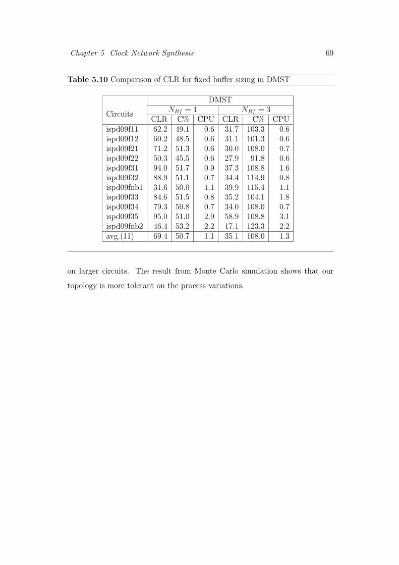
Chapter 5 Clock Network Synthesis 69
Table 5.10 Comparison of CLR for fixed buffer sizing in DMST
DMSTNBf = 1 NBf = 3
CircuitsCLR C% CPU CLR C% CPU
ispd09f11 62.2 49.1 0.6 31.7 103.3 0.6ispd09f12 60.2 48.5 0.6 31.1 101.3 0.6ispd09f21 71.2 51.3 0.6 30.0 108.0 0.7ispd09f22 50.3 45.5 0.6 27.9 91.8 0.6ispd09f31 94.0 51.7 0.9 37.3 108.8 1.6ispd09f32 88.9 51.1 0.7 34.4 114.9 0.8ispd09fnb1 31.6 50.0 1.1 39.9 115.4 1.1ispd09f33 84.6 51.5 0.8 35.2 104.1 1.8ispd09f34 79.3 50.8 0.7 34.0 108.0 0.7ispd09f35 95.0 51.0 2.9 58.9 108.8 3.1ispd09fnb2 46.4 53.2 2.2 17.1 123.3 2.2avg.(11) 69.4 50.7 1.1 35.1 108.0 1.3
on larger circuits. The result from Monte Carlo simulation shows that our
topology is more tolerant on the process variations.
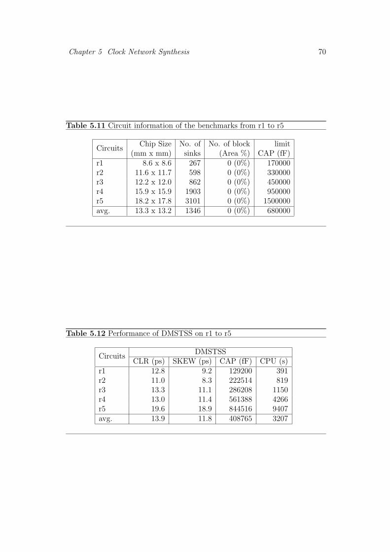
Chapter 5 Clock Network Synthesis 70
Table 5.11 Circuit information of the benchmarks from r1 to r5
Chip Size No. of No. of block limitCircuits
(mm x mm) sinks (Area %) CAP (fF)r1 8.6 x 8.6 267 0 (0%) 170000r2 11.6 x 11.7 598 0 (0%) 330000r3 12.2 x 12.0 862 0 (0%) 450000r4 15.9 x 15.9 1903 0 (0%) 950000r5 18.2 x 17.8 3101 0 (0%) 1500000avg. 13.3 x 13.2 1346 0 (0%) 680000
Table 5.12 Performance of DMSTSS on r1 to r5
DMSTSSCircuits
CLR (ps) SKEW (ps) CAP (fF) CPU (s)r1 12.8 9.2 129200 391r2 11.0 8.3 222514 819r3 13.3 11.1 286208 1150r4 13.0 11.4 561388 4266r5 19.6 18.9 844516 9407avg. 13.9 11.8 408765 3207
Chapter 6
Clock Gating Design
6.1 Overview
In this chapter, we propose two novel synthesizers, HKPUst and HKPUcg,
to construct a binary clock tree in a bottom-up course. Simultaneous opti-
mization on the clock skew and the power dissipation is applied. The topology
generator is responsible for a buffered and gated clock tree, and the clock gates
are inserted concurrently. In our work, the downstream masking information
of subtrees is taken into account during each merging step. Two algorithms
of topology generation, dual-MST [55] and NNS [24], are applied in our work.
The according cost functions are improved for power awareness, therefore it
can reduce the switched capacitance. HKPUcg applies the same slew rate
(Cd ≤ 20 × Cg) as previous works [65, 11]. Besides, in HKPUst we perform
a more strict slew constraint (≤ 100ps) along the whole clock network. Thus
the constraint on buffer and gate location is emphasized. The experimental
results show that our method can greatly reduce the power consumption of the
clock network with proper gate insertion. Meanwhile, the nominal clock skew
is guaranteed to be exact zero. With the simulation of SPICE, the resultant
skew is still acceptable.
71

Chapter 6 Clock Gating Design 72
6.2 Problem Formulation
6.2.1 Clock Tree and Controller Tree
Let T = V,E denote the clock tree. V = vi|i = 1, 2, . . . ,mv is the set of
nodes, and E = ej|j = 1, 2, . . . ,mv − 1 is the set of clock edges between the
node vj and its corresponding parent. Let |ej| denote the length of the edge
ej. Apparently, for the root node there will be no edge assigned. Let G =
gi|i = 1, 2, . . . ,mv − 1 denote the set of gates. The gate gj is assigned to be
on the edge ej masking the node vj directly. We use S = vk|k = 1, 2, . . . ,ms
(where ms < mv) to denote the set of modules (the sinks, or leaf nodes). The
rest (mv − ms) nodes are named internal nodes. The root is said to be at level
0. Node vi is said to be at level ni if there are ni edges on the path from vi
to the root of the tree. Moreover, we assume that the topology of the clock
tree is full binary. Every internal node has exactly two children. The skew
of T is the difference between the longest signal delay and the shortest signal
delay from the source to any sinks. As proposed in [65], we assume that the
control logic is located at the center of the chip. Star routing is also applied in
the controller tree, denoted as T ctr. A control edge ENi in T ctr will transmit
the enable signal to the respective gate gi on the edge ei in the clock tree T .
An example of a clock tree T as well as its controller tree T ctr is shown in
figure 6.1.
During the operating time of a circuit, each module will have its active and
idle times. It is usually specified as different activity patterns. The activity
patterns can be obtained by the simulation of the design at the behavioral
level [27]. Let Ai denote the activity pattern of the node vi. It is a binary
string with 1s indicating the active periods and 0s indicating the idle periods
of a sink or an internal node. If vi is a sink node, we can directly obtain Ai
from the benchmark file. Otherwise, suppose vi to be an internal node with
two children nodes vL and vR accordingly. The clock signal at vi must be
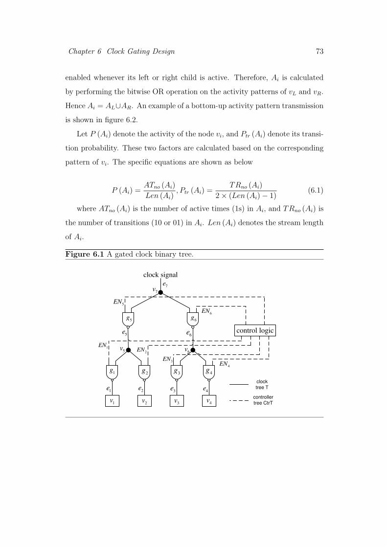
Chapter 6 Clock Gating Design 73
enabled whenever its left or right child is active. Therefore, Ai is calculated
by performing the bitwise OR operation on the activity patterns of vL and vR.
Hence Ai = AL∪AR. An example of a bottom-up activity pattern transmission
is shown in figure 6.2.
Let P (Ai) denote the activity of the node vi, and Ptr (Ai) denote its transi-
tion probability. These two factors are calculated based on the corresponding
pattern of vi. The specific equations are shown as below
P (Ai) =ATno (Ai)
Len (Ai), Ptr (Ai) =
TRno (Ai)
2 × (Len (Ai) − 1)(6.1)
where ATno (Ai) is the number of active times (1s) in Ai, and TRno (Ai) is
the number of transitions (10 or 01) in Ai. Len (Ai) denotes the stream length
of Ai.
Figure 6.1 A gated clock binary tree.
control logic
1v 2v 3v 4v
6v
7v
1g 2g 3g 4g
5g 6g
1e 2e 3e 4e
1EN
5e 6e
clock signal
5v
7e
2EN
3EN4EN
5EN
6EN
clock
tree T
controller
tree CtrT
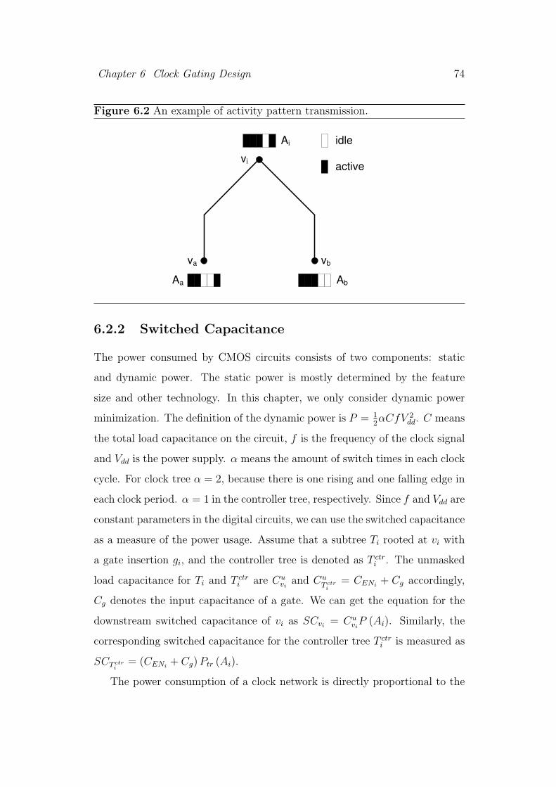
Chapter 6 Clock Gating Design 74
Figure 6.2 An example of activity pattern transmission.
Aa
va vb
Ab
Ai
vi
idle
active
6.2.2 Switched Capacitance
The power consumed by CMOS circuits consists of two components: static
and dynamic power. The static power is mostly determined by the feature
size and other technology. In this chapter, we only consider dynamic power
minimization. The definition of the dynamic power is P = 12αCfV 2
dd. C means
the total load capacitance on the circuit, f is the frequency of the clock signal
and Vdd is the power supply. α means the amount of switch times in each clock
cycle. For clock tree α = 2, because there is one rising and one falling edge in
each clock period. α = 1 in the controller tree, respectively. Since f and Vdd are
constant parameters in the digital circuits, we can use the switched capacitance
as a measure of the power usage. Assume that a subtree Ti rooted at vi with
a gate insertion gi, and the controller tree is denoted as T ctri . The unmasked
load capacitance for Ti and T ctri are Cu
viand Cu
T ctri
= CENi+ Cg accordingly,
Cg denotes the input capacitance of a gate. We can get the equation for the
downstream switched capacitance of vi as SCvi= Cu
viP (Ai). Similarly, the
corresponding switched capacitance for the controller tree T ctri is measured as
SCT ctri
= (CENi+ Cg) Ptr (Ai).
The power consumption of a clock network is directly proportional to the
Chapter 6 Clock Gating Design 75
average switched capacitance for each clock cycle. The total switched capaci-
tance is contributed by a gated and buffered clock tree T and a controller tree
T ctr. In order to reduce the switching activity, modules and clock tree sections
can be disabled by clock gates during their inactive clock periods. From the
above example, we can see that the original capacitance of node vi is Cuvi. With
gate gi inserted at vi, the resultant switched capacitance is SCvi+ SCT ctr
i. If
Cuvi
< SCvi+ SCT ctr
i, the capacitance will be reduced with the insertion of gi.
A power aware clock tree topology with proper buffer and gate insertion will
efficiently reduce the switched capacitance, hence cut down the power usage
of the circuits.
Given a testcase with the physical location and the activity pattern of all
the modules, together with the circuit models of wire/buffer/gate, the objective
of our work is to construct a buffered and gated clock network T as well as a
controller network T ctr. Subject to the two constraints of zero skew and slew
rate constraint, the resultant total switched capacitance SCT + SCT ctr should
be minimized.
6.3 Methodology
In our clock gating work, two synthesizers, HKPUcg and HKPUst, are pro-
posed. HKPUcg applies the same slew rate (Cd ≤ 20 × Cg) as previous works [65,
11]. The driver capacitance of every buffer/gate cannot exceed 20 times of a
gate input capacitance. Besides, in HKPUst we perform a more strict slew
constraint (≤ 100ps) along the whole clock network. Slew table is constructed
in advance to provide driving ability at each gate/buffer insertion point. We
build our clock trees based on two topology generation methods. In HKPUcg,
NNS [24] is applied with an newly improved power aware cost function. Ev-
ery time the pair of nodes with the minimum cost are merged together. In
HKPUst, the dual-MST construction method [55] is applied also with newly

Chapter 6 Clock Gating Design 76
improved cost function. The resulting clock tree is close to a full symmetry.
As a result of the cost improvement, the according topology can result in lower
power usage. A recursive buffer/clock gate insertion method is developed for
bottom-up merging. Blockage handling technique from [55] is also involved,
because the buffers and gates cannot be placed inside blockage regions. Elmore
model [26] is applied for clock delay computation, and DME technique [3, 10]
is applied for wirelength minimization. Thus, segment is used instead of point
to represent the set of merging location, and deferred embedding is applied to
reduce total wirelength.
6.3.1 Power Aware Topology Generation
In order to save the power, the nodes with a bigger similarity of activity pat-
terns should have a higher priority to be matched. Assume va and vb to be a
pair of two nodes, as shown in figure 6.2. If the corresponding activity pat-
terns Aa and Ab are similar, the resulted activity Ai will have a shorter active
period, and smaller power cost will be caused. Besides the concerns on activ-
ity patterns, an estimation of the merging cost Pwr (va, vb) is also required.
This can be determined in multiple ways. For instance, we can actually merge
the two nodes together to obtain the exact connection information. However,
exact buffer insertion and wire balancing are performed, which will cost longer
time. Instead, we develop a new method for potential switched capacitance
estimation. The Manhattan distance between the nodes va and vb is denoted
by D(va, vb). The Elmore delay difference of these two nodes is denoted by
DLY (va, vb). The delay and power consumption for unit wirelength are de-
noted by ρD and ρP respectively, which are computed in advance for simulation
reference. If DLY (va,vb)ρD
is smaller than D(va, vb), then the two nodes can be
merged without snaking wire involved, and the corresponding equation for
Chapter 6 Clock Gating Design 77
power cost computation is shown as below
Pwr (va, vb) = ρP × D(va, vb) × P (Ai) (6.2)
Otherwise, snaking will be included, as shown in the following equation
Pwr (va, vb) = ρP ×DLY (va, vb)
ρD
× P (Ai) (6.3)
An improved power aware dual-MST matching technique is developed for
HKPUst. A specific definition of a geometric matching of one iteration can
be found in [41]. The detailed description is shown in procedure 1 of chap-
ter 5. It is a weighted perfect matching approach. Given a set of nodes
V = v1, v2 . . . vm, we first construct a complete graph G = V,E. Let |V |
and |E| denote the number of nodes and edges in the graph G, so|V | = m.
Since G is a complete graph, every pair of two nodes vi, vj is connected by an
edge ei,j, E = e1,2, e1,3 . . . em−1,m and |E| = m(m−1)2
. The cost of matching
two nodes vi and vj is denoted as fc (ei,j). Let M denote the matching result
of G. M is composed of a group of edges and it is a subset of E. The maximal
pairing cost of M is denoted as Cmax and defined as below. We will get close
to a symmetric clock tree by reducing Cmax in each level. The merging cost
fDMSTc (va, vb) for dual-MST is shown as below. α and β are the weights of the
Manhattan distance and the estimated power cost, respectively.
fDMSTc (va, vb) = α × D(va, vb) + β × Pwr(va, vb) (6.4)
Similarly, an improved power aware NNS matching technique is developed
for HKPUcg. We compute the two edges of ea and eb based on zero skew
concerns. The cost function is an estimation of the resultant total switched
capacitance, which is shown as below
fNNSc (va, vb) = |ea| × P (Aa) + |eb| × P (Ab) (6.5)

Chapter 6 Clock Gating Design 78
By means of these weighted cost functions, the node pairs with a bigger
similarity of switching activity and a shorter distance will have a higher priority
to be matched. Our approach of topology generation is based on concurrent
gate insertion, therefore the downstream information of the two merging nodes
are accurate.
6.3.2 Concurrent Gate and Buffer Insertion
A recursive buffer and gate insertion technique is developed for two objectives:
(1) slew rate constraint (2) power usage reduction. Buffers are utilized for
power supply to restrict the signal transition time, and clock gate insertion
can reduce the switched capacitance by disabling idle sections. We model
the buffer and gate with according attributes for Elmore delay computation.
Some previous works [15] already proposed to construct a buffered clock tree
with zero clock skew. In our work, we apply similar approach for both buffer
and clock gate insertion. The input/output capacitance and resistance of the
buffers and clock gates should be obtained first. Hence, the delay of wire,
buffers and clock gates can be computed based on Elmore RC model.
In HKPUst, we try to maintain the level of buffers and gates of every source-
to-sink clock path exactly the same. During the procedure of the bottom-up
binary merging, we first examine the two downstream levels of gates. If they
differ by two or more, a penalty cost will be engaged. Such matching result
will probably be discarded due to the huge cost. Buffer levels will be balanced
accordingly. By means of this level balancing, the clock skew will be reduced
significantly, and the negative effect caused by signal variation will be reduced.
Here we will describe our technique of gate insertion based on a determined
matching result. We first define three different kinds of gate insertion. They
are virtual gate insertion at the upstream level, temporal gate insertion at the
current level and none gate insertion. Temporal insertion is controlled by the
Chapter 6 Clock Gating Design 79
balancing of gate levels, which will be further divided into two kinds of single
gate insertion and one kind of back-to-back double gates insertion. The inser-
tion of a gate is assumed to be closest to the internal merging node for switched
capacitance minimization. Since DME technique is applied in our work, we
assume the middle point of the merging segment to be the gate location. The
comparison among the three assumption of gate insertion are based on the re-
sulting switched capacitance, which are SCvir, SCtmp and SCnon, respectively.
If the power consumption of the virtual insertion or the none insertion is the
smallest, no insertion of any gate will definitely result in less switched capaci-
tance compared to the choice of temporal gate insertion. Therefore, we discard
any insertion of gates at the current level. Otherwise, temporal gate insertion
will probably reduce the switched capacitance rather than the others, and here
we will accept the insertion of gates.
An example is shown in figure 6.2. The activity Ai equals to Aa ∪ Ab.
The edge connection between each of the two nodes to the merging node are
denoted as ea and eb. Ceaand Ceb
are their corresponding capacitance cost.
The equations to compute the three resulting switched capacitance are shown
as below
SCvir (va, vb) = (Cua + Cea
+ Cub + Ceb
) × P (Ai) + CuT ctr
i× Ptr (Ai) (6.6)
SCtmp (va, vb) = (Cua + Cea
) × P (Aa) + CuT ctr
a× Ptr (Aa) + Cu
b + Ceb(6.7)
SCnon (va, vb) = Cua + Cea
+ Cub + Ceb
(6.8)
Notice that here we only describe the equation of SCtmp for a single gate
insertion at node va. The other two equations can be derived in a similar way.
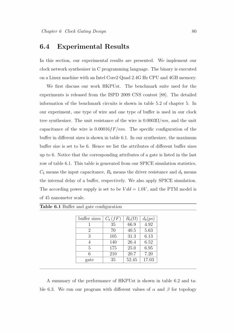
Chapter 6 Clock Gating Design 80
6.4 Experimental Results
In this section, our experimental results are presented. We implement our
clock network synthesizer in C programming language. The binary is executed
on a Linux machine with an Intel Core2 Quad 2.4G Hz CPU and 4GB memory.
We first discuss our work HKPUst. The benchmark suite used for the
experiments is released from the ISPD 2009 CNS contest [88]. The detailed
information of the benchmark circuits is shown in table 5.2 of chapter 5. In
our experiment, one type of wire and one type of buffer is used in our clock
tree synthesizer. The unit resistance of the wire is 0.0003Ω/nm, and the unit
capacitance of the wire is 0.00016fF/nm. The specific configuration of the
buffer in different sizes is shown in table 6.1. In our synthesizer, the maximum
buffer size is set to be 6. Hence we list the attributes of different buffer sizes
up to 6. Notice that the corresponding attributes of a gate is listed in the last
row of table 6.1. This table is generated from our SPICE simulation statistics.
Cb means the input capacitance, Rb means the driver resistance and db means
the internal delay of a buffer, respectively. We also apply SPICE simulation.
The according power supply is set to be V dd = 1.0V , and the PTM model is
of 45 nanometer scale.
Table 6.1 Buffer and gate configuration
buffer sizes Cb (fF ) Rb(Ω) db(ps)1 35 66.9 4.922 70 40.5 5.633 105 31.3 6.134 140 26.4 6.525 175 25.0 6.956 210 20.7 7.20
gate 35 52.45 17.03
A summary of the performance of HKPUst is shown in table 6.2 and ta-
ble 6.3. We run our program with different values of α and β for topology
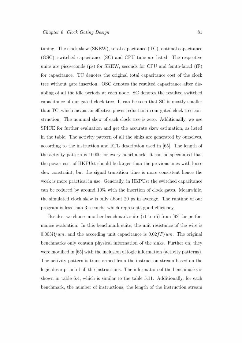
Chapter 6 Clock Gating Design 81
tuning. The clock skew (SKEW), total capacitance (TC), optimal capacitance
(OSC), switched capacitance (SC) and CPU time are listed. The respective
units are picoseconds (ps) for SKEW, seconds for CPU and femto-farad (fF)
for capacitance. TC denotes the original total capacitance cost of the clock
tree without gate insertion. OSC denotes the resulted capacitance after dis-
abling of all the idle periods at each node. SC denotes the resulted switched
capacitance of our gated clock tree. It can be seen that SC is mostly smaller
than TC, which means an effective power reduction in our gated clock tree con-
struction. The nominal skew of each clock tree is zero. Additionally, we use
SPICE for further evaluation and get the accurate skew estimation, as listed
in the table. The activity pattern of all the sinks are generated by ourselves,
according to the instruction and RTL description used in [65]. The length of
the activity pattern is 10000 for every benchmark. It can be speculated that
the power cost of HKPUst should be larger than the previous ones with loose
slew constraint, but the signal transition time is more consistent hence the
work is more practical in use. Generally, in HKPUst the switched capacitance
can be reduced by around 10% with the insertion of clock gates. Meanwhile,
the simulated clock skew is only about 20 ps in average. The runtime of our
program is less than 3 seconds, which represents good efficiency.
Besides, we choose another benchmark suite (r1 to r5) from [92] for perfor-
mance evaluation. In this benchmark suite, the unit resistance of the wire is
0.003Ω/um, and the according unit capacitance is 0.02fF/um. The original
benchmarks only contain physical information of the sinks. Further on, they
were modified in [65] with the inclusion of logic information (activity patterns).
The activity pattern is transformed from the instruction stream based on the
logic description of all the instructions. The information of the benchmarks is
shown in table 6.4, which is similar to the table 5.11. Additionally, for each
benchmark, the number of instructions, the length of the instruction stream
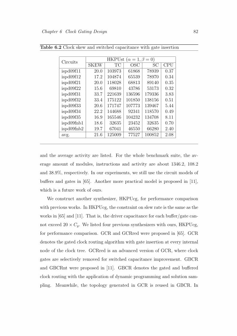
Chapter 6 Clock Gating Design 82
Table 6.2 Clock skew and switched capacitance with gate insertion
HKPUst (α = 1, β = 0)Circuits
SKEW TC OSC SC CPUispd09f11 20.0 103973 61868 78939 0.37ispd09f12 17.2 104874 65539 78970 0.34ispd09f21 20.0 118028 68813 89140 0.35ispd09f22 15.6 69810 43786 53173 0.32ispd09f31 33.7 221639 136596 179336 3.83ispd09f32 33.4 175122 101850 138156 0.51ispd09f33 20.6 171747 107773 139467 5.44ispd09f34 22.2 144688 92341 118570 0.49ispd09f35 16.9 165546 104232 134708 8.11ispd09fnb1 18.6 32635 23452 32635 0.70ispd09fnb2 19.7 67041 46550 66280 2.40avg. 21.6 125009 77527 100852 2.08
and the average activity are listed. For the whole benchmark suite, the av-
erage amount of modules, instructions and activity are about 1346.2, 108.2
and 38.9%, respectively. In our experiments, we still use the circuit models of
buffers and gates in [65]. Another more practical model is proposed in [11],
which is a future work of ours.
We construct another synthesizer, HKPUcg, for performance comparison
with previous works. In HKPUcg, the constraint on slew rate is the same as the
works in [65] and [11]. That is, the driver capacitance for each buffer/gate can-
not exceed 20 × Cg. We listed four previous synthesizers with ours, HKPUcg,
for performance comparison. GCR and GCRred were proposed in [65]. GCR
denotes the gated clock routing algorithm with gate insertion at every internal
node of the clock tree. GCRred is an advanced version of GCR, where clock
gates are selectively removed for switched capacitance improvement. GBCR
and GBCRnt were proposed in [11]. GBCR denotes the gated and buffered
clock routing with the application of dynamic programming and solution sam-
pling. Meanwhile, the topology generated in GCR is reused in GBCR. In
Chapter 6 Clock Gating Design 83
Table 6.3 Clock skew and switched capacitance with gate insertion
HKPUst (α = 2, β = 1)Circuits
SKEW TC OSC SC CPUispd09f11 20.0 103973 61868 78939 0.37ispd09f12 17.2 104874 65539 78970 0.34ispd09f21 20.0 118028 68813 89140 0.35ispd09f22 15.6 69810 43786 53173 0.32ispd09f31 33.7 221639 136596 179336 3.83ispd09f32 33.4 175122 101850 138156 0.51ispd09f33 20.6 171747 107773 139467 5.44ispd09f34 22.2 144688 92341 118570 0.49ispd09f35 16.9 165546 104232 134708 8.11ispd09fnb1 18.6 32635 23452 32635 0.70ispd09fnb2 19.7 67041 46550 66280 2.40avg. 21.6 125009 77527 100852 2.08
Table 6.4 Circuit information of the benchmarks from r1 to r5
Chip Size No. No. Inst. AverageCircuits
(mm x mm) Sinks Inst. Length Activity (%)r1 8.6 x 8.6 267 64 10000 39.86r2 11.6 x 11.7 598 89 10000 39.60r3 12.2 x 12.0 862 108 10000 36.91r4 15.9 x 15.9 1903 120 10000 40.56r5 18.2 x 17.8 3101 160 10000 37.42avg. 13.3 x 13.2 1346.2 108.2 10000 38.87
GBCRnt, a new topology was generated for performance improvement. The
applied benchmark suite are exactly the same for the above five research works.
The performance of the five clock gating research works are shown in table 6.5,
table 6.6 and table 6.7. In these two tables, the total switched capacitance cost
(SC in pF ), total wirelength of the clock tree (CLK in mm) and the controller
tree (CTR in mm), and the CPU runtime (CPU in sec) are listed for compar-
ison.
It can be observed that GCR has the largest switched capacitance thus the
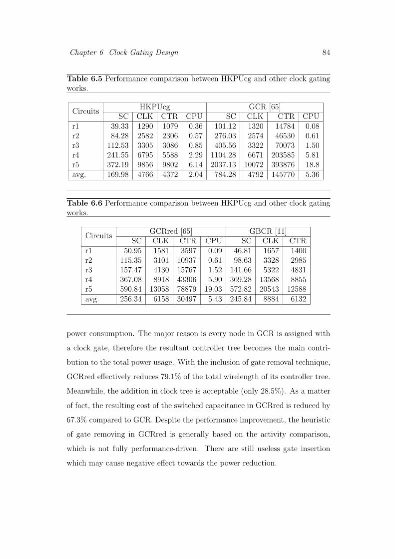
Chapter 6 Clock Gating Design 84
Table 6.5 Performance comparison between HKPUcg and other clock gatingworks.
HKPUcg GCR [65]Circuits
SC CLK CTR CPU SC CLK CTR CPUr1 39.33 1290 1079 0.36 101.12 1320 14784 0.08r2 84.28 2582 2306 0.57 276.03 2574 46530 0.61r3 112.53 3305 3086 0.85 405.56 3322 70073 1.50r4 241.55 6795 5588 2.29 1104.28 6671 203585 5.81r5 372.19 9856 9802 6.14 2037.13 10072 393876 18.8avg. 169.98 4766 4372 2.04 784.28 4792 145770 5.36
Table 6.6 Performance comparison between HKPUcg and other clock gatingworks.
GCRred [65] GBCR [11]Circuits
SC CLK CTR CPU SC CLK CTRr1 50.95 1581 3597 0.09 46.81 1657 1400r2 115.35 3101 10937 0.61 98.63 3328 2985r3 157.47 4130 15767 1.52 141.66 5322 4831r4 367.08 8918 43306 5.90 369.28 13568 8855r5 590.84 13058 78879 19.03 572.82 20543 12588avg. 256.34 6158 30497 5.43 245.84 8884 6132
power consumption. The major reason is every node in GCR is assigned with
a clock gate, therefore the resultant controller tree becomes the main contri-
bution to the total power usage. With the inclusion of gate removal technique,
GCRred effectively reduces 79.1% of the total wirelength of its controller tree.
Meanwhile, the addition in clock tree is acceptable (only 28.5%). As a matter
of fact, the resulting cost of the switched capacitance in GCRred is reduced by
67.3% compared to GCR. Despite the performance improvement, the heuristic
of gate removing in GCRred is generally based on the activity comparison,
which is not fully performance-driven. There are still useless gate insertion
which may cause negative effect towards the power reduction.
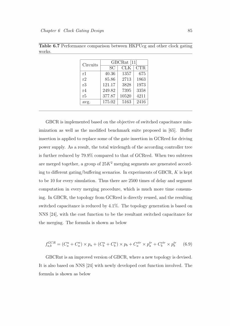
Chapter 6 Clock Gating Design 85
Table 6.7 Performance comparison between HKPUcg and other clock gatingworks.
GBCRnt [11]Circuits
SC CLK CTRr1 40.36 1357 675r2 85.86 2713 1863r3 121.17 3828 1973r4 249.82 7395 3358r5 377.87 10520 4211avg. 175.02 5163 2416
GBCR is implemented based on the objective of switched capacitance min-
imization as well as the modified benchmark suite proposed in [65]. Buffer
insertion is applied to replace some of the gate insertion in GCRred for driving
power supply. As a result, the total wirelength of the according controller tree
is further reduced by 79.9% compared to that of GCRred. When two subtrees
are merged together, a group of 25K2 merging segments are generated accord-
ing to different gating/buffering scenarios. In experiments of GBCR, K is kept
to be 10 for every simulation. Thus there are 2500 times of delay and segment
computation in every merging procedure, which is much more time consum-
ing. In GBCR, the topology from GCRred is directly reused, and the resulting
switched capacitance is reduced by 4.1%. The topology generation is based on
NNS [24], with the cost function to be the resultant switched capacitance for
the merging. The formula is shown as below
fGCRa,b = (Cu
a + Cna ) × pa + (Cu
b + Cnb ) × pb + Cctr
a × ptra + Cctr
b × ptrb (6.9)
GBCRnt is an improved version of GBCR, where a new topology is devised.
It is also based on NNS [24] with newly developed cost function involved. The
formula is shown as below
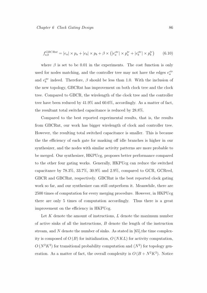
Chapter 6 Clock Gating Design 86
fGBCRnta,b = |ea| × pa + |eb| × pb + β ×
(
|ectra | × ptr
a + |ectrb | × ptr
b
)
(6.10)
where β is set to be 0.01 in the experiments. The cost function is only
used for nodes matching, and the controller tree may not have the edges ectra
and ectrb indeed. Therefore, β should be less than 1.0. With the inclusion of
the new topology, GBCRnt has improvement on both clock tree and the clock
tree. Compared to GBCR, the wirelength of the clock tree and the controller
tree have been reduced by 41.9% and 60.6%, accordingly. As a matter of fact,
the resultant total switched capacitance is reduced by 28.8%.
Compared to the best reported experimental results, that is, the results
from GBCRnt, our work has bigger wirelength of clock and controller tree.
However, the resulting total switched capacitance is smaller. This is because
the the efficiency of each gate for masking off idle branches is higher in our
synthesizer, and the nodes with similar activity patterns are more probable to
be merged. Our synthesizer, HKPUcg, proposes better performance compared
to the other four gating works. Generally, HKPUcg can reduce the switched
capacitance by 78.3%, 33.7%, 30.9% and 2.9%, compared to GCR, GCRred,
GBCR and GBCRnt, respectively. GBCRnt is the best reported clock gating
work so far, and our synthesizer can still outperform it. Meanwhile, there are
2500 times of computation for every merging procedure. However, in HKPUcg
there are only 5 times of computation accordingly. Thus there is a great
improvement on the efficiency in HKPUcg.
Let K denote the amount of instructions, L denote the maximum number
of active sinks of all the instructions, B denote the length of the instruction
stream, and N denote the number of sinks. As stated in [65],the time complex-
ity is composed of O (B) for initialization, O (NKL) for activity computation,
O (N2K2) for transitional probability computation and (N2) for topology gen-
eration. As a matter of fact, the overall complexity is O (B + N2K2). Notice
Chapter 6 Clock Gating Design 87
that N2 is only the average complexity of topology generation, the complexity
of the worst case is still N3. The complexity of the work in [11] is stated as
O (N3 + BN), which is worse with the operation on the whole activity pattern
at each merging node.
In our work, we use a K × K matrix to restore the instruction transition-
module activation table (ITMAT [65]) for every sink, the total additional mem-
ory cost is NK2. During the bottom-up merging procedure, it is just necessary
to compute the OR result of the ITMAT of two nodes, with the complexity of
K2. Therefore, the total complexity for transitional probability computation is
only NK2. Notice that the ITMAT matrix of any nodes can be reused by their
parent nodes, so the total extra cost on memory is still NK2. As a result, the
overall complexity of our clock gating work is reduced to O (B + N2 + NK2).
The experimental results regarding the major three metrics (SC, CLK and
CTR) of GCR, GCRred, GBCR and GBCRnt are all obtained from [11] (the
results of GCR and GCRred reported in [65] have some errors in the com-
putation of switched capacitance, which are verified and corrected in [11]).
Additionally, we obtain the debugged source code of the work in [65]. For the
comparison of runtime, we execute the according program of GCR and GCRred
in our platform. In table 6.5 and table 6.6, the CPU runtime of HKPUcg, GCR
and GCRred is also listed. It is shown that due to the improvement on com-
plexity of our program (from O (B + N2K2) to (B + NK2 + N2)), the average
runtime is reduced by 61.9%, compared to the runtime of GCR and GCRred.
The runtime of GBCR and GBCRnt have not been obtained for comparison.
6.5 Summary
Power saving and clock skew are two major concerns in clock network synthe-
sis. A power aware topology generation is proposed with improved design on
the cost function. Meanwhile, a concurrent buffer/gate insertion technique is

Chapter 6 Clock Gating Design 88
proposed. It can distribute the gate properly in high efficiency. This is devel-
oped in order to optimize the power dissipation of a clock distribution network.
In both of the two proposed synthesizers, HKPUcg and HKPUst, zero clock
skew is guaranteed. Experimental results show that our method can greatly
reduce the switched capacitance hence reduce the power consumption of the
clock network. Compared to the previous clock gating works, HKPUcg have
better performance on power saving. Meanwhile, the resultant simulated clock
skew of HKPUst under SPICE is still acceptable, with no slew rate violation
engaged.
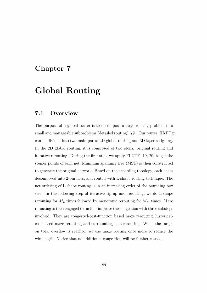
Chapter 7
Global Routing
7.1 Overview
The purpose of a global router is to decompose a large routing problem into
small and manageable subproblems (detailed routing) [79]. Our router, HKPUgr,
can be divided into two main parts: 2D global routing and 3D layer assigning.
In the 2D global routing, it is composed of two steps: original routing and
iterative rerouting. During the first step, we apply FLUTE [19, 20] to get the
steiner points of each net, Minimum spanning tree (MST) is then constructed
to generate the original network. Based on the according topology, each net is
decomposed into 2-pin nets, and routed with L-shape routing technique. The
net ordering of L-shape routing is in an increasing order of the bounding box
size. In the following step of iterative rip-up and rerouting, we do L-shape
rerouting for ML times followed by monotonic rerouting for MM times. Maze
rerouting is then engaged to further improve the congestion with three substeps
involved. They are congested-cost-function based maze rerouting, historical-
cost-based maze rerouting and surrounding nets rerouting. When the target
on total overflow is reached, we use maze routing once more to reduce the
wirelength. Notice that no additional congestion will be further caused.
89

Chapter 7 Global Routing 90
Table 7.1 Notations in global routing
Notation Descriptionni The ith net of the net listpi The ith pin in a netsi The ith steiner point in a net
Kpi,Ksi
The node structure of the ith pin or steiner pointsub(pi, pj) The subnet between pi and pj
Gi The ith grid pointE(i,j) The edge between Gi and Gj
cGiThe accumulated cost of Gi
cEi,jThe accumulated cost of Ei,j
c(Gi,Gj) The cost of the edge between Gi and Gj
cbnd The unit cost of a bendingFE(i) The cost of the edge E with usage of iCE(i) The first order of FE(i)
pi The probability to be occupied with usage of i
7.2 Problem Formulation
The chip is decomposed into rectangular global bins of the same size. All
the pins are then distributed into their according bins. An example of chip
decomposition is shown in figure 7.1(a). In figure 7.1(b), each vertex represents
a global bin (grid point), and each edge (grid edge) connecting two adjacent
bins represents the boundary in figure 7.1(a). In global routing, only inter-bin
connections are implemented. The implementation of inner-bin connections
are completed in detailed routing.
Let N denote the set of nets, N = n1, n2, . . . , n|N |. Let Pi denote the set
of pins for the ith net, Pi = p1i , p
2i , . . . , p
|Pi|i . We use ei to denote the edge i,
and the set of edges is denoted by E. We use OFeito denote the overflow on
the edge ei. ceiand dei
are used to denote the capacity and demand of edge ei,
respectively. On the edge ei, the overflow is defined as the exceeding amount
of demand towards its capacity. If deiis greater than cei
, OFeiequals dei
− cei.
Otherwise, OFeiequals zero.
The global routing problem is usually formulated as below. Given a grid
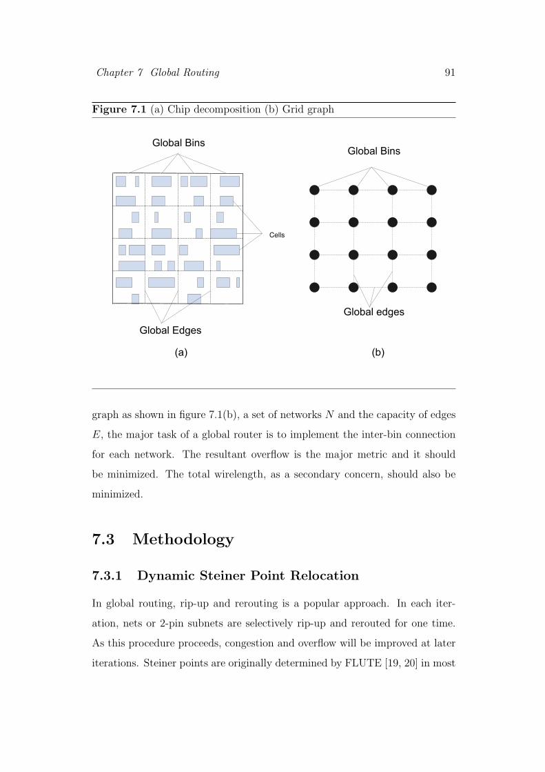
Chapter 7 Global Routing 91
Figure 7.1 (a) Chip decomposition (b) Grid graph
Cells
graph as shown in figure 7.1(b), a set of networks N and the capacity of edges
E, the major task of a global router is to implement the inter-bin connection
for each network. The resultant overflow is the major metric and it should
be minimized. The total wirelength, as a secondary concern, should also be
minimized.
7.3 Methodology
7.3.1 Dynamic Steiner Point Relocation
In global routing, rip-up and rerouting is a popular approach. In each iter-
ation, nets or 2-pin subnets are selectively rip-up and rerouted for one time.
As this procedure proceeds, congestion and overflow will be improved at later
iterations. Steiner points are originally determined by FLUTE [19, 20] in most
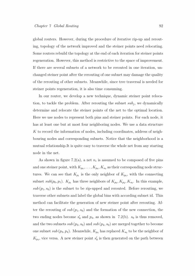
Chapter 7 Global Routing 92
global routers. However, during the procedure of iterative rip-up and rerout-
ing, topology of the network improved and the steiner points need relocating.
Some routers rebuild the topology at the end of each iteration for steiner points
regeneration. However, this method is restrictive to the space of improvement.
If there are several subnets of a network to be rerouted in one iteration, un-
changed steiner point after the rerouting of one subnet may damage the quality
of the rerouting of other subnets. Meanwhile, since tree traversal is needed for
steiner points regeneration, it is also time consuming.
In our router, we develop a new technique, dynamic steiner point reloca-
tion, to tackle the problem. After rerouting the subnet subj, we dynamically
determine and relocate the steiner points of the net to the optimal location.
Here we use nodes to represent both pins and steiner points. For each node, it
has at least one but at most four neighboring nodes. We use a data structure
K to record the information of nodes, including coordinates, address of neigh-
bouring nodes and corresponding subnets. Notice that the neighborhood is a
mutual relationship.It is quite easy to traverse the whole net from any starting
node in the net.
As shown in figure 7.2(a), a net ni is assumed to be composed of five pins
and one steiner point, with Kp0, . . . , Kp4
, Ks0as their corresponding node struc-
tures. We can see that Kp1is the only neighbor of Kp0
, with the connecting
subnet sub(p0, p1). Kp1has three neighbors of Kp0
, Kp2, Ks0
. In this example,
sub (p1, s0) is the subnet to be rip-upped and rerouted. Before rerouting, we
traverse other subnets and label the global bins with according subnet id. This
method can facilitate the generation of new steiner point after rerouting. Af-
ter the rerouting of sub (p1, s0) and the formation of the new connection, the
two ending nodes become s′0 and p4, as shown in 7.2(b). s0 is thus removed,
and the two subnets sub (p3, s0) and sub (p4, s0) are merged together to become
one subnet sub (p3, p4). Meanwhile, Kp4has replaced Ks0
to be the neighbor of
Kp3, vice versa. A new steiner point s′0 is then generated on the path between
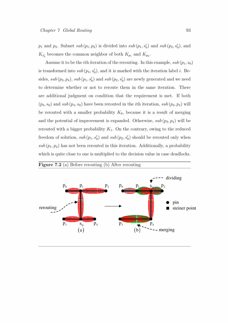
Chapter 7 Global Routing 93
p1 and p2. Subnet sub (p1, p2) is divided into sub (p1, s′0) and sub (p2, s
′0), and
Ks′0
becomes the common neighbor of both Kp1and Kp2
.
Assume it to be the ith iteration of the rerouting. In this example, sub (p1, s0)
is transformed into sub (p4, s′0), and it is marked with the iteration label i. Be-
sides, sub (p3, p4), sub (p1, s′0) and sub (p2, s
′0) are newly generated and we need
to determine whether or not to reroute them in the same iteration. There
are additional judgment on condition that the requirement is met. If both
(p3, s0) and sub (p4, s0) have been rerouted in the ith iteration, sub (p3, p4) will
be rerouted with a smaller probability K0, because it is a result of merging
and the potential of improvement is expanded. Otherwise, sub (p3, p4) will be
rerouted with a bigger probability K1. On the contrary, owing to the reduced
freedom of solution, sub (p1, s′0) and sub (p2, s
′0) should be rerouted only when
sub (p1, p2) has not been rerouted in this iteration. Additionally, a probability
which is quite close to one is multiplied to the decision value in case deadlocks.
Figure 7.2 (a) Before rerouting (b) After rerouting
pin
steiner point
a
0p 1p 2p
3p 4p0s
rerouting
b
0p 1p 2p
3p 4p
0s
merging
dividing

Chapter 7 Global Routing 94
7.3.2 Edge-based Monotonic and Maze Routing
In global routing, layer assignment is applied after completing the planar inter-
bin connection of all the networks. If the edges of the planar connection
of a network are assigned into different layers, inter-layer connection (via) is
necessary to keep the connectivity of the network.
In the planar view, the resultant amount of via for each network is generally
determined by its number of planar bendings. In the modern global routers,
the factor of bendings is usually involved in the cost function to improve the
performan of routing and rip-up rerouting.
Traditional maze routers are based on the propagation of grid points, and
it utilize a queue to maintain the points which have been reached. In each
step, the point with the minimal cost is popped from the queue, and we call it
the major point. The the adjacent four points are propagated from the major
point, and each of them is labelled with an accumulated cost value, as well as a
parent point. Such procedure continues until we reach the sink terminal. This
approach can get the optimal result, if the cost is a sum of the two weighted
factors, congestion and wirelength. Nonetheless, with the amount of bendings
as an additioanl factor, the result generated by the maze router is no longer
optimum.
In the global routing, the cost function is usually composed of the following
three factors: congestion, wirelength and bendings, shown as below
Cost = #cong + #wire + #bend (7.1)
In this section, we present an example to describe the shortcomings of maze
router based on point propagation. As shown in figure 7.3 (a), G0, . . . G3
denotes the grid points, and cGidenotes the cost of Gi. Suppose that G0 and
G1 have already been reached, with cost values cG0and cG1
accordingly. At
the point G2, there are two solutions available. c0G2
= cG0+ c(G0,G2) and c1
G2=

Chapter 7 Global Routing 95
cG1+c(G1,G2). Assume that c0
G2> c1
G2, then G2 is labelled with value of c1
G2, and
G1 becomes the parent of G2. In the next turn, G3 is propagated from G2 with
a cost of cG3= c1
G2+ cbnd + c(G2,G3). This procedure appears very reasonable,
because we get the solution (G3 → G2 → G1) for G3. However, due to the
additional bending cost, it is possible that c0G2
+ c(G2,G3) < c1G2
+ cbnd + c(G2,G3).
Therefore, the path (G3 → G2 → G0) is a better choice than (G3 → G2 → G1),
but it cannot be acquired through traditional maze routing approach.
We develop a new maze router based on the propagation of grid edges,
optimum result based on equation 7.1 can always be obtained. E(i,j) denotes
the edge connecting the points Gi and Gj, and cEi,jdenotes the respective
propagation cost. In our method, we use edge as the basic propagation unit.
During the routing, each edge in the grid is assigned with a cost value and a
parent edge. The edge cost is also an accumulated value from the source edge.
We apply a priority queue as a storage for the edges. During each time of
rerouting, the target two pin net will be removed, and the net is decomposed
into to two subnets : a source subnet and a sink subnet. The basic object of
rerouting is to connect the two subnets together. At the beginning, we traverse
the source subnet and store all the the adjacent edges into the queue. In each
step of propagation, one edge is extracted from the top of the queue, which
has the minimal cost value. This edge has one of its two adjacent points as the
starting point, and the other one as the ending point. The other three edges
adjacent to the ending point are the target edges for propagation. Notice that
the one of the three with the same direction as the original edge is assured to
have the optimal solution. However, the other two perpendicular edges would
possibly be updated with better solution in the following steps, due to the
bending factors.
An example of edge propagation is shown in figure 7.4(a). Suppose that
E(0,2) and E1,2 have already been reached and stored in the queue. Suppose
that E0,2 is currently the major edge, and E1,2 is still in the queue, thus

Chapter 7 Global Routing 96
cE0,2< cE1,2
. Two edges E(2,4), E(2,3) can be propagated in this turn. E(2,3)
is in the same direction with E(0,2), so cE2,3= cE0,2
+ cG2,G3is determined to
be the accumulated cost value of E2,3. Notice that no further update for E(2,3)
is necessary, because any cost cx from the following major edges will be larger
than cE0,2, therefore cx+cG2,G3
> cE0,2+cG2,G3
. Therefore, E0,2 → E2,3 is proved
to be the optimal solution for E2,3. Meanwhile, E2,4 is in the perpendicular
direction with E0,2, and c′E2,4= cE0,2
+ cG2,G4+ cbnd become the cost of E2,4,
and E0,2 → E2,4 is a conditional solution for E2,4. In the next step, E1,2
becomes the major edge, as shown in figure 7.4(b). If c′E2,4> cE1,2
+ cE2,4,
E1,2 → E2,4 turns out to be a better solution than E0,2 → E2,4, and it is
also the optimal solution for E2,4. E2,4 is then updated with the parent path
E1,2 and the respective cost, and it won’t be updated in future. Generally,
in the new approach the optimal solution can be certainly reached, and the
computational cost for updating is reduced compared to the traditional maze
router.
Figure 7.3 Comparison of two solutions
0G
1G
2G3G
optimal
solution
actual
solution
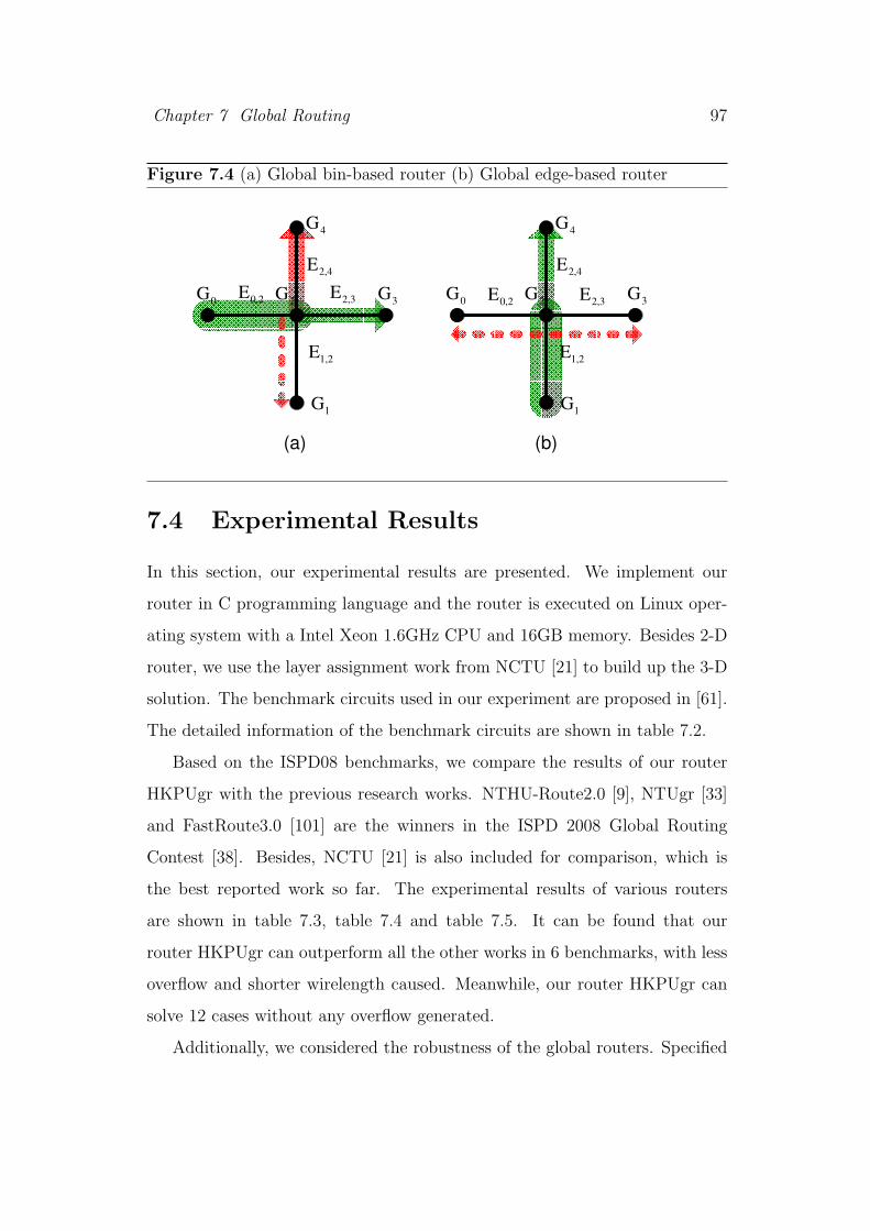
Chapter 7 Global Routing 97
Figure 7.4 (a) Global bin-based router (b) Global edge-based router
0G
1G
2G 3G0,2E
1,2E
2,3E
2,4E
4G
0G
1G
2G 3G0,2E
1,2E
2,3E
2,4E
4G
(a) (b)
7.4 Experimental Results
In this section, our experimental results are presented. We implement our
router in C programming language and the router is executed on Linux oper-
ating system with a Intel Xeon 1.6GHz CPU and 16GB memory. Besides 2-D
router, we use the layer assignment work from NCTU [21] to build up the 3-D
solution. The benchmark circuits used in our experiment are proposed in [61].
The detailed information of the benchmark circuits are shown in table 7.2.
Based on the ISPD08 benchmarks, we compare the results of our router
HKPUgr with the previous research works. NTHU-Route2.0 [9], NTUgr [33]
and FastRoute3.0 [101] are the winners in the ISPD 2008 Global Routing
Contest [38]. Besides, NCTU [21] is also included for comparison, which is
the best reported work so far. The experimental results of various routers
are shown in table 7.3, table 7.4 and table 7.5. It can be found that our
router HKPUgr can outperform all the other works in 6 benchmarks, with less
overflow and shorter wirelength caused. Meanwhile, our router HKPUgr can
solve 12 cases without any overflow generated.
Additionally, we considered the robustness of the global routers. Specified
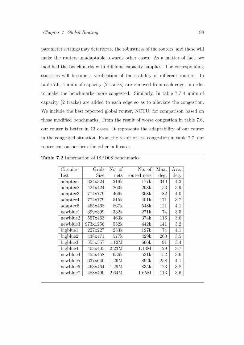
Chapter 7 Global Routing 98
parameter settings may deteriorate the robustness of the routers, and these will
make the routers unadaptable towards other cases. As a matter of fact, we
modified the benchmarks with different capacity supplies. The corresponding
statistics will become a verification of the stability of different routers. In
table 7.6, 4 units of capacity (2 tracks) are removed from each edge, in order
to make the benchmarks more congested. Similarly, In table 7.7 4 units of
capacity (2 tracks) are added to each edge so as to alleviate the congestion.
We include the best reported global router, NCTU, for comparison based on
those modified benchmarks. From the result of worse congestion in table 7.6,
our router is better in 13 cases. It represents the adaptability of our router
in the congested situation. From the result of less congestion in table 7.7, our
router can outperform the other in 6 cases.
Table 7.2 Information of ISPD08 benchmarks
Circuits Grids No. of No. of Max. Ave.List Size nets routed nets deg. deg.adaptec1 324x324 219k 177k 340 4.2adaptec2 424x424 260k 208k 153 3.9adaptec3 774x779 466k 368k 82 4.0adaptec4 774x779 515k 401k 171 3.7adaptec5 465x468 867k 548k 121 4.1newblue1 399x399 332k 271k 74 3.5newblue2 557x463 463k 374k 116 3.6newblue3 973x1256 552k 442k 141 3.2bigblue1 227x227 283k 197k 74 4.1bigblue2 438x471 577k 429k 260 3.5bigblue3 555x557 1.12M 666k 91 3.4bigblue4 403x405 2.23M 1.13M 129 3.7newblue4 455x458 636k 531k 152 3.6newblue5 637x640 1.26M 892k 258 4.1newblue6 463x464 1.29M 835k 123 3.8newblue7 488x490 2.64M 1.65M 113 3.6
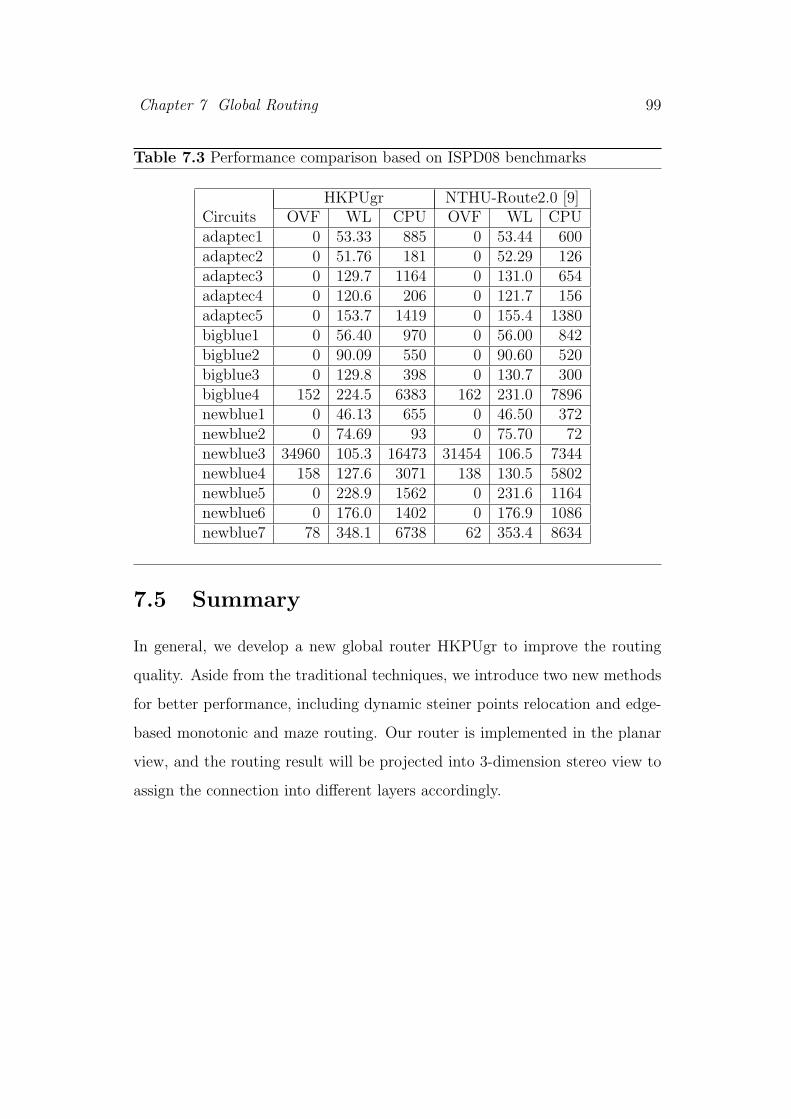
Chapter 7 Global Routing 99
Table 7.3 Performance comparison based on ISPD08 benchmarks
HKPUgr NTHU-Route2.0 [9]Circuits OVF WL CPU OVF WL CPUadaptec1 0 53.33 885 0 53.44 600adaptec2 0 51.76 181 0 52.29 126adaptec3 0 129.7 1164 0 131.0 654adaptec4 0 120.6 206 0 121.7 156adaptec5 0 153.7 1419 0 155.4 1380bigblue1 0 56.40 970 0 56.00 842bigblue2 0 90.09 550 0 90.60 520bigblue3 0 129.8 398 0 130.7 300bigblue4 152 224.5 6383 162 231.0 7896newblue1 0 46.13 655 0 46.50 372newblue2 0 74.69 93 0 75.70 72newblue3 34960 105.3 16473 31454 106.5 7344newblue4 158 127.6 3071 138 130.5 5802newblue5 0 228.9 1562 0 231.6 1164newblue6 0 176.0 1402 0 176.9 1086newblue7 78 348.1 6738 62 353.4 8634
7.5 Summary
In general, we develop a new global router HKPUgr to improve the routing
quality. Aside from the traditional techniques, we introduce two new methods
for better performance, including dynamic steiner points relocation and edge-
based monotonic and maze routing. Our router is implemented in the planar
view, and the routing result will be projected into 3-dimension stereo view to
assign the connection into different layers accordingly.
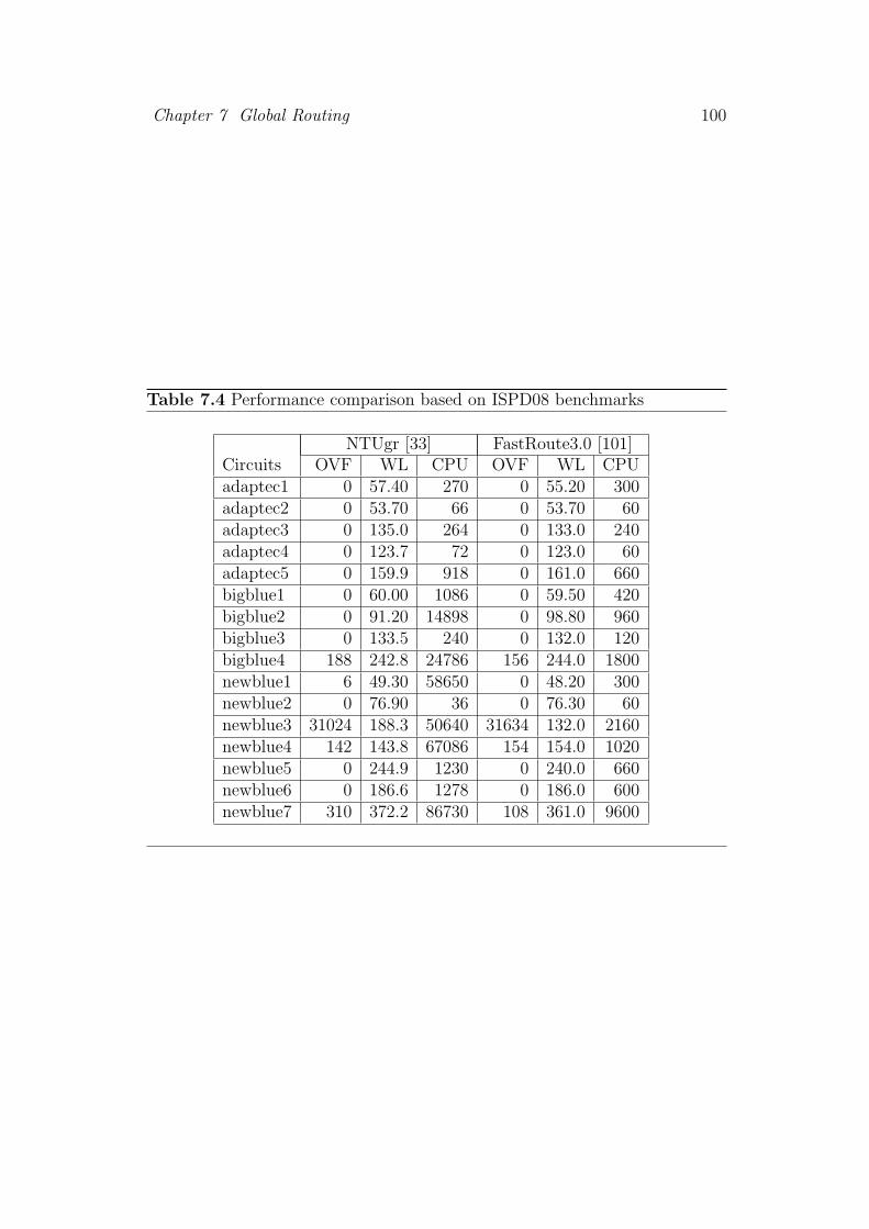
Chapter 7 Global Routing 100
Table 7.4 Performance comparison based on ISPD08 benchmarks
NTUgr [33] FastRoute3.0 [101]Circuits OVF WL CPU OVF WL CPUadaptec1 0 57.40 270 0 55.20 300adaptec2 0 53.70 66 0 53.70 60adaptec3 0 135.0 264 0 133.0 240adaptec4 0 123.7 72 0 123.0 60adaptec5 0 159.9 918 0 161.0 660bigblue1 0 60.00 1086 0 59.50 420bigblue2 0 91.20 14898 0 98.80 960bigblue3 0 133.5 240 0 132.0 120bigblue4 188 242.8 24786 156 244.0 1800newblue1 6 49.30 58650 0 48.20 300newblue2 0 76.90 36 0 76.30 60newblue3 31024 188.3 50640 31634 132.0 2160newblue4 142 143.8 67086 154 154.0 1020newblue5 0 244.9 1230 0 240.0 660newblue6 0 186.6 1278 0 186.0 600newblue7 310 372.2 86730 108 361.0 9600
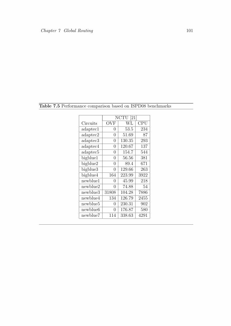
Chapter 7 Global Routing 101
Table 7.5 Performance comparison based on ISPD08 benchmarks
NCTU [21]Circuits OVF WL CPUadaptec1 0 53.5 234adaptec2 0 51.69 87adaptec3 0 130.35 293adaptec4 0 120.67 137adaptec5 0 154.7 544bigblue1 0 56.56 381bigblue2 0 89.4 671bigblue3 0 129.66 263bigblue4 164 223.99 3922newblue1 0 45.99 218newblue2 0 74.88 54newblue3 31808 104.28 7886newblue4 134 126.79 2455newblue5 0 230.31 902newblue6 0 176.87 580newblue7 114 338.63 4291
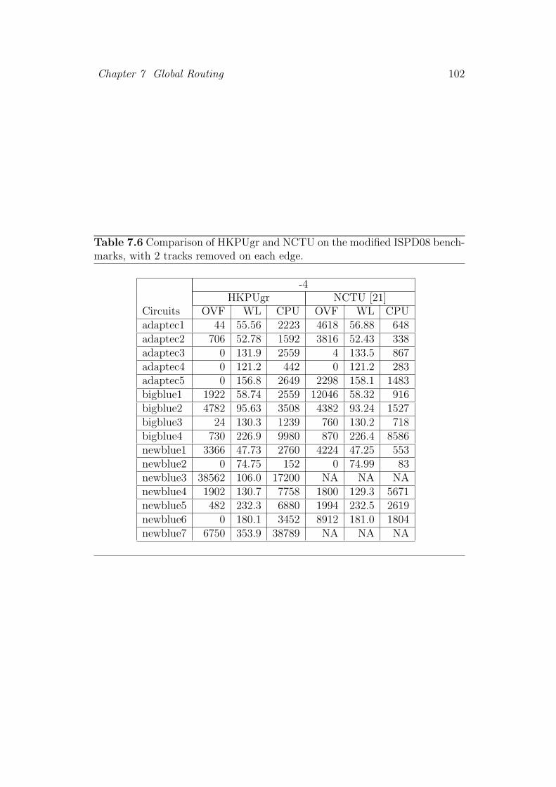
Chapter 7 Global Routing 102
Table 7.6 Comparison of HKPUgr and NCTU on the modified ISPD08 bench-marks, with 2 tracks removed on each edge.
-4HKPUgr NCTU [21]
Circuits OVF WL CPU OVF WL CPUadaptec1 44 55.56 2223 4618 56.88 648adaptec2 706 52.78 1592 3816 52.43 338adaptec3 0 131.9 2559 4 133.5 867adaptec4 0 121.2 442 0 121.2 283adaptec5 0 156.8 2649 2298 158.1 1483bigblue1 1922 58.74 2559 12046 58.32 916bigblue2 4782 95.63 3508 4382 93.24 1527bigblue3 24 130.3 1239 760 130.2 718bigblue4 730 226.9 9980 870 226.4 8586newblue1 3366 47.73 2760 4224 47.25 553newblue2 0 74.75 152 0 74.99 83newblue3 38562 106.0 17200 NA NA NAnewblue4 1902 130.7 7758 1800 129.3 5671newblue5 482 232.3 6880 1994 232.5 2619newblue6 0 180.1 3452 8912 181.0 1804newblue7 6750 353.9 38789 NA NA NA
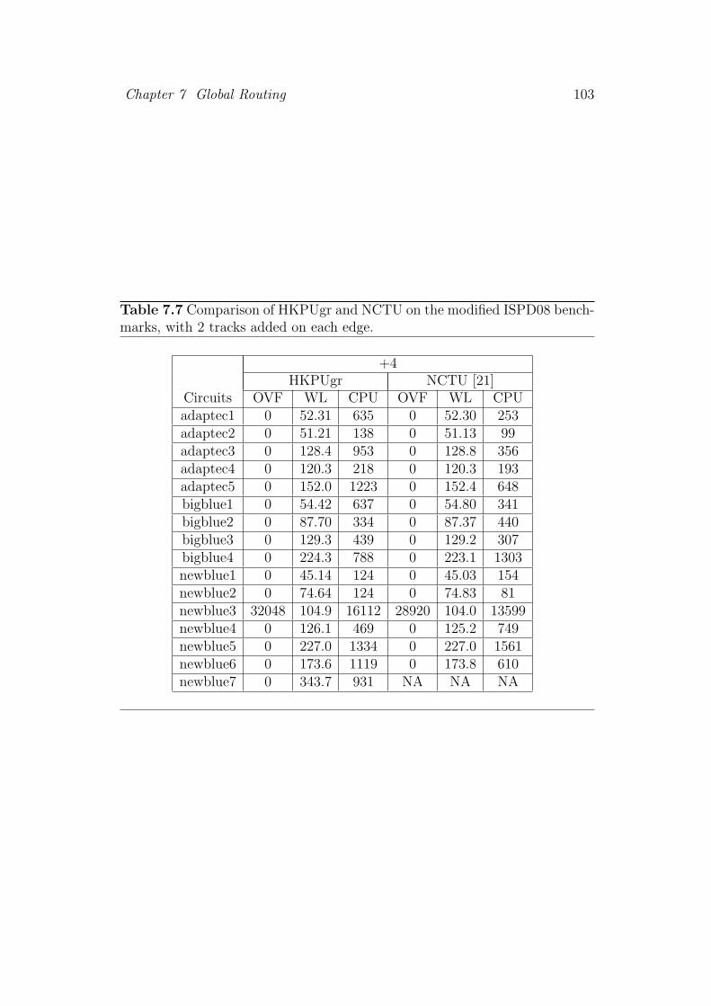
Chapter 7 Global Routing 103
Table 7.7 Comparison of HKPUgr and NCTU on the modified ISPD08 bench-marks, with 2 tracks added on each edge.
+4HKPUgr NCTU [21]
Circuits OVF WL CPU OVF WL CPUadaptec1 0 52.31 635 0 52.30 253adaptec2 0 51.21 138 0 51.13 99adaptec3 0 128.4 953 0 128.8 356adaptec4 0 120.3 218 0 120.3 193adaptec5 0 152.0 1223 0 152.4 648bigblue1 0 54.42 637 0 54.80 341bigblue2 0 87.70 334 0 87.37 440bigblue3 0 129.3 439 0 129.2 307bigblue4 0 224.3 788 0 223.1 1303newblue1 0 45.14 124 0 45.03 154newblue2 0 74.64 124 0 74.83 81newblue3 32048 104.9 16112 28920 104.0 13599newblue4 0 126.1 469 0 125.2 749newblue5 0 227.0 1334 0 227.0 1561newblue6 0 173.6 1119 0 173.8 610newblue7 0 343.7 931 NA NA NA
Chapter 8
Conclusion
In this thesis, we have introduced some fundamental ideas regarding the re-
search topic of routability of the VLSI physical design. Specifically, our focus
is located at congestion prediction, clock network synthesis, clock gating de-
sign and global routing. In the literature review at chapter 3, we can see that
plenty of research works have been proposed by earlier researchers to address
the problem of routability. Based on the previous achievements, our work has
proposed novel techniques to further improve the performance and enhance
the routability.
Congestion prediction is applied at early stages of the physical design. It
provides the designer with an estimation of the routability on the chip. Based
on the analysis of previous estimation models, we develop three models in
chapter 4 for accuracy improvement. SMD model is the fastest technique with
the least amount of computation involved, only the tiles inside the bounding
box of each subnet are included. Further on, detour model pays extra atten-
tion to the surrounding tiles, which becomes adaptive to the over-congested
areas. 3-step approach is composed of routing selection and congestion redis-
tribution. The result is of enhanced similarity with that of the technique of
iterative rip-up and rerouting, which is widely applied in the modern global
routers. From the experimental results, it can be concluded that our models
have made significant improvements on the accuracy of prediction, compared
104
Chapter 8 Conclusion 105
the the previous models.
In terms of the requirements proposed in the ISPD 2009 CNS contest, we
develop two clock network synthesizers (DMST and DMSTSS) in chapter 5
with six novel techniques involved. A new method of topology construction,
dual-MST, is proposed to build up a tree structure that is very close to a
symmetric one. This approach can reduce the sensitivity of the clock skew
against voltage variation effectively. Moreover, the developments on hierarchi-
cal buffer sizing, iterative buffer insertion and blockage handling techniques
further improve the performance and reduce the power consumption. From
slew table, the signal transition time can be reduced by the reference of driver
ability. In DMSTSS, a method of merging point relocation is developed. Based
on the delay estimation of SPICE simulation, clock skew is further reduced by
the relocation. Experimental results show that our DMSTSS can outperform
all the previous synthesizers with smaller CLR and program runtime in every
benchmark. Meanwhile, the three constraints on slew rate, buffer distribution
and total capacitance are followed.
For the objective of power saving in the clock network, enough concerns
should be taken during the procedure of synthesis. In our work, we achieve
the target of power saving by logic gates insertion to mask off the inactive
modules and branches. We propose two gated synthesizers (HKPUcg and HK-
PUst) in chapter 6 with several novel techniques. Improved implementation on
topology generation are proposed. Besides, a newly developed buffer/gate in-
sertion technique are devised to reduce the power dissipation. Compared to the
previous clock gating works, the resultant switched capacitance of HKPUcg is
smaller. Meanwhile, the complexity of our algorithm is smaller, which is shown
by the reduced CPU runtime in HKPUcg. In HKPUst, the buffered/gated so-
lution can reduce the switched capacitance compared to that of its original
buffered solution, and the resulting clock skew is still acceptable.
In the stage of global routing, routability is fully emphasized. A new global

Chapter 8 Conclusion 106
router, HKPUgr, is proposed in chapter 7 aiming at a better quality of rout-
ing design. Our router is built up upon the technique of iterative rip-up and
rerouting. Furthermore, we introduce two new methods to improve the perfor-
mance, including dynamic steiner points relocation and edge-based monotonic
and maze routing. With fast reduction on overflow, the amount of wirelength
and via connection can also be reduced by our approach. From the experi-
mental results, we can see that most of the benchmarks can be solved by our
approach with a shorter wirelength.
Routability has dominant effect on the quality of signal transmission and
the timing delay of the circuit. Therefore, exclusive concerns should be in-
volved throughout the whole VLSI physical design procedure. In particular,
we achieve the improvement on routability in several correlative steps. Dur-
ing the early designing time, our prediction models will provide the designer
with a good estimation on the routability of the packing results, so as to
facilitate routing the networks in the subsequent routing procedure. In clock
network synthesis, our contribution on proper buffer distribution will maintain
the routability of the clock tree. Additionally, clock gating is an associating
step of CNS aiming at power reduction. Subsequently, global routing imple-
ments the connection of the rest of the networks inside the area of the chip.
The newly proposed techniques will shorten the total wirelength, in order to
reduce the signal delay and improve the routability.
Bibliography
[1] C. Albrecht. Global Routing by New Approximation Algorithms for
Multicommodity Flow. IEEE Transactions on Computer-Aided Design
of Integrated Circuits and Systems, 20(5):622 – 631, May 2001.
[2] H. Anway, G. Farnham, and R. Reid. Plint Layout Systems for VLSI
Chips. In Proceedings of IEEE/ACM Design Automation Conference,
pages 449 – 452, 1985.
[3] K. D. Boese and A. B. Kahng. Zero-Skew Clock Routing Trees with Min-
imum Wirelength. In Proceedings of 5th the Annual IEEE International
ASIC Conference and Exhibit, pages 17 – 21, 1992.
[4] M. Burstein and R. Pelavin. Hierarchical Wire Routing. In Proceedings of
IEEE/ACM International Conference on Computer Aided Design, pages
223 – 234, 1983.
[5] A. E. Caldwell, A. B. Kahng, and I. L. Markov. Can Recursive Bisection
Produce Routable Placements? In Proceedings of IEEE/ACM Design
Automation Conference, pages 477–482, 2000.
[6] R. C. Carden and C. K. Cheng. A Global Router Using an Efficient
Approximate Multicommodity Multiterminal Flow Algorithm. In Pro-
ceedings of IEEE/ACM Design Automation Conference, pages 316 – 321,
1991.
107
[7] C. C. Chang, J. Cong, D. Z. Pan, and X. Yuan. Interconnect-Driven
Floorplanning with Fast Global Wiring Planning and Optimization. In
Proceedings of SRC Tech. Conference, November 2000.
[8] C.-M. Chang, S.-H. Huang, Y.-K. Ho, J.-Z. Lin, H.-P. Wang, and Y.-S.
Lu. Type-Matching Clock Tree for Zero Skew Clock Gating. In Pro-
ceedings of IEEE/ACM Design Automation Conference, pages 714–719,
June 2008.
[9] Y.-J. Chang, Y.-T. Lee, and T.-C. Wang. NTHU-Route 2.0: A Fast
and Stable Global Router. In Proceedings of IEEE/ACM International
Conference on Computer Aided Design, pages 338 – 343, November 2008.
[10] T. H. Chao, Y. C. Hsu, J. M. Ho, and A. B. Kahng. Zero Skew Clock
Routing with Minimum Wirelength. IEEE Transactions on Circuits
and Systems II: Analog and Digital Signal Processing., 39(11):799 – 814,
1992.
[11] W. C. Chao and W. K. Mak. Low-Power Gated and Buffered Clock
Network Construction. ACM Transactions on Design Automation of
Electronic Systems, 13(1), January 2008.
[12] R. Chaturvedi and J. Hu. Buffered Clock Tree for High Quality IC
design. In International Symposium on Quality Electronic Design, pages
381 – 386, 2004.
[13] C. Chen, C. Kang, and M. Sarrafzadeh. Activity-Sensitive Clock Tree
Construction for Low Power. In International Symposium on Low Power
Electronics and Design, pages 279 – 282, 2002.
108
[14] H. M. Chen, H. Zhou, F. Y. Young, D. Wong, H. H. Yang, and N. Sher-
vani. Integrated Floorplanning and Interconnect Planning. In Proceed-
ings of IEEE/ACM International Conference on Computer Aided De-
sign, pages 354 – 357, November 1999.
[15] Y. P. Chen and D. F. Wong. An Algorithm for Zero-Skew Clock Tree
Routing with Buffer Insertion. In Proceedings of European Design and
Test Conference, pages 230–236, 1996.
[16] C. K. Cheng and E. S. Kuh. Module Placement Based on Resistive
Network Optimization. IEEE Transactions on Computer-Aided Design
of Integrated Circuits and Systems, 3:218 – 225, 1984.
[17] J. D. Cho and M. Sarrafzadeh. A Buffer Distribution Algorithm for High-
Speed Clock Routing. In Proceedings of IEEE/ACM Design Automation
Conference, pages 537–543, June 1993.
[18] M. Cho and D. Z. Pan. BoxRouter: A New Global Router Based on Box
Expansion and Progressive ILP. In Proceedings of IEEE/ACM Design
Automation Conference, pages 373 – 378, July 2006.
[19] C. Chu. FLUTE: Fast Lookup Table Based Wirelength Estimation Tech-
nique. In Proceedings of IEEE/ACM International Conference on Com-
puter Aided Design, pages 696 – 701, November 2004.
[20] C. Chu and Y.-C. Wong. FLUTE: Fast Lookup Table Based Rectilinear
Steiner Minimal Tree Algorithm for VLSI Design. IEEE Transactions on
Computer-Aided Design of Integrated Circuits and Systems, 27(1):257 –
268, January 2008.
[21] K.-R. Dai, W.-H. Liu, and Y.-L. Li. Efficient Simulated Evolution Based
Rerouting and Congestion-Relaxed Layer Assignment on 3-D Global
109
Routing. In Proceedings of Asia and South Pacific Design Automation
Conference, pages 570–575, January 2009.
[22] M. Donno, A. Ivaldi, L. Benini, and E. Macii. Clock-Tree Power Op-
timization based on RTL Clock-Gating. In Proceedings of IEEE/ACM
Design Automation Conference, pages 622 – 627, June 2003.
[23] A. E. Dunlop and B. W. Kernighan. A Procedure for Placement of
Standard Cell VLSI Circuits. IEEE Transactions on Computer-Aided
Design of Integrated Circuits and Systems, 4:92 – 98, 1985.
[24] M. Edahiro. A Clustering-Based Optimization Algorithm in Zero-Skew
Routings. In Proceedings of IEEE/ACM Design Automation Conference,
pages 612–616, July 1993.
[25] M. Edahiro and T. Yoshimura. Minimum Path-Length Equi-Distant
Routing. In Proceedings of IEEE Asia-Pacific Conference on Circuits
and Systems, pages 41–46, 1992.
[26] W. C. Elmore. The Transient Response of Damped Linear Networks
with Particular Regard to Wide Band Amplifiers. Journal of Applied
Physics, 19(1):55–63, January 1948.
[27] A. H. Farrahi, C. Chen, A. Srivastava, G. Tellez, and M. Sarrafzadeh.
Activity-Driven Clock Design. IEEE Transactions on Computer-Aided
Design of Integrated Circuits and Systems, 20(6):705 – 714, June 2001.
[28] C. M. Fiduccia and R. M. Mattheyses. A Linear Time Heuristic for
Improving Network Partitions. In Proceedings of IEEE/ACM Design
Automation Conference, pages 175 – 181, 1982.
[29] J.-R. Gao, P.-C. Wu, and T.-C. Wang. A New Global Router for Modern
Designs. In Proceedings of Asia and South Pacific Design Automation
Conference, pages 232 – 237, January 2008.
110
[30] David Garrett, Mircea Stan, and Alvar Dean. Challenges in Clockgating
for a Low Power ASIC Methodology. In International Symposium on
Low Power Electronics and Design, pages 176 – 181, 1999.
[31] L. P. P. P. Ginneken. Buffer Placement in Distributed RC-tree Networks
for Minimal Elmore Delay. In International Symposium on Circuits and
Systems, pages 865–868, May 1990.
[32] R. T. Hadsell and P. H. Madden. Improved Global Routing through Con-
gestion Estimation. In Proceedings of IEEE/ACM Design Automation
Conference, pages 28 – 31, June 2003.
[33] C.-H. Hsu, H.-Y. Chen, and Y.-W. Chang. Multi-layer Global Routing
Considering Via and Wire Capacities. In Proceedings of IEEE/ACM
International Conference on Computer Aided Design, pages 350 – 355,
November 2008.
[34] C. P. Hsu. APLS2: A Standard Cell Layout System for Double-layer
Metal Technology. In Proceedings of IEEE/ACM Design Automation
Conference, pages 443 – 448, 1985.
[35] F. K. Hwang, D. S. Richards, and P. Winter. Steiner Tree Problems.
Networks, 22(1):55 – 89, October 2006.
[36] ISPD. http://vlsicad.eecs.umich.edu/BK/ISPD02bench/. 2002.
[37] ISPD. http://www.sigda.org/ispd2007/rcontest/. 2007.
[38] ISPD. http://www.sigda.org/ispd2008/contests/ispd08rc.html. 2008.
[39] ISPD. http://www.sigda.org/ispd/contests/09/ispd09cts.html. 2009.
[40] M. A. B. Jackson, A. Srinivasan, and E. S. Kuh. Clock Routing for
High-Performance ICs. In Proceedings of IEEE/ACM Design Automa-
tion Conference, pages 573–579, June 1990.
111
[41] A. Kahng, J. Cong, and G. Robins. High-Performance Clock Routing
Based on Recursive Geometric Matching. In Proceedings of IEEE/ACM
Design Automation Conference, pages 322–327, July 1991.
[42] A. B. Kahng and X. Xu. Accurate Pseudo-Constructive Wirelength and
Congestion Estimation. In Proceedings of International Workshop on
System Level Interconnect Prediction, pages 61 – 68, April 2003.
[43] R. M. Karp, F. T. Leighton, R. L. Rivest, C. D. Thompson, U. Vazi-
rani, and V. Vazirani. Global Wire Routing in Two-Dimensional Arrays.
Algorithmica, 2:113 – 129, 1987.
[44] R. Kastner, E. Bozorgzadeh, and M. Sarrafzadeh. Pattern Routing:
Use and Theory for Increasing Predictability and Avoiding Coupling.
IEEE Transactions on Computer-Aided Design of Integrated Circuits and
Systems, 21(7):777 – 790, July 2002.
[45] B. W. Keinighan and S. Lin. An Efficient Heuristic Procedure for Par-
titioning Graphs. Bell System Technical Journal, 49:291 – 307, January
1970.
[46] T. Kitahara, F. Minami, T. Ueda, K. Usami, S. Nishio, M. Mruakata,
and T. Mitsuhashi. A Clock-Gating Method for Low-Power LSI Design.
In Proceedings of Asia and South Pacific Design Automation Conference,
pages 307 – 312, January 1998.
[47] K. Kozminski and E. Kinnen. Rectangular Dual of Planar Graphs. Net-
works, 15:145 – 157, 1985.
[48] B. Krishnamurthy. An Improved Min-Cut Algorithm for Partitioning
VLSI Networks. IEEE Transactions on Computers, 33:438 – 446, 1984.
[49] Kusnadi and J. D. Carothers. A Method of Measuring Nets Routability
for MCMs General Area Routing Problems. In Proceedings of ACM
112
International Symposium on Physical Design, pages 186 – 194, March
1999.
[50] S. T. W. Lai, E. F. Y. Young, and C. C. N. Chu. A New and Efficient
Congestion Evaluation Model in Floorplanning: Wire Density Control
with Twin Binary Trees. In European Design and Test Conference, April
2003.
[51] J. F. Lee and C. K. Wong. A Performance-Aimed Cell Compactor with
Automatic Jogs. IEEE Transactions on Computer-Aided Design of In-
tegrated Circuits and Systems, 11:1495 – 1507, 1992.
[52] I.-M. Liu, T.-L. Chou, D. F. Wong, and A. Aziz. Zero-Skew Clock Tree
Construction by Simultaneous Routing, Wire Sizing and Buffer Insertion.
In Proceedings of IEEE/ACM International Conference on Computer
Aided Design, pages 33–38, Nov 2000.
[53] W. H. Liu, Y. L. Li, and H. C. Chen. Minimizing Clock Latency Range
in Robust Clock Tree Synthesis. In Proceedings of Asia and South Pacific
Design Automation Conference, pages 389 – 394, January 2010.
[54] J. Lou, S. Krishnamoorthy, and H. S. Sheng. Estimating Routing Con-
gestion Using Probabilistic Analysis. In Proceedings of ACM Interna-
tional Symposium on Physical Design, pages 112–117, March 2001.
[55] J. Lu, W. K. Chow, C. W. Sham, and E. F. Y. Young. A Dual-MST
Approach for Clock Network Synthesis. In Proceedings of Asia and South
Pacific Design Automation Conference, pages 467 – 473, January 2010.
[56] Y. Luo, J. Yu, J. Yang, and L. Bhuyan. Low Power Network Proces-
sor Design Using Clock Gating. In Proceedings of IEEE/ACM Design
Automation Conference, pages 712 – 715, June 2005.
113
[57] Y. C. Ma, X. L. Hong, S. Q. Dong, S. Chen, Y. C. Cai, C. K. Cheng, and
J. Gu. Dynamic Global Buffer Planning Optimization Based on Detail
Block Locating and Congestion Analysis. In Proceedings of IEEE/ACM
Design Automation Conference, pages 806 – 811, July 2003.
[58] M. D. Moffitt. MaizeRouter: Engineering an Effective Global Router. In
Proceedings of Asia and South Pacific Design Automation Conference,
pages 226 – 231, January 2008.
[59] M. D. Moffitt. MaizeRouter: Engineering an Effective Global Router.
IEEE Transactions on Computer-Aided Design of Integrated Circuits and
Systems, 27(11):2017 – 2026, November 2008.
[60] M. D. Moffitt, J. A. Roy, and I. L. Markov. The Coming of Age of (Aca-
demic) Global Routing. In Proceedings of ACM International Symposium
on Physical Design, pages 148 – 155, April 2008.
[61] G.-J. Nam, C. Sze, and M. Yildiz. The ISPD Global Routing Benchmark
Suite. In Proceedings of ACM International Symposium on Physical De-
sign, pages 156 – 159, April 2008.
[62] G.-J. Nam, M. Yildiz, D. Z. Pan, and P. H. Madden. ISPD Placement
Contest Updates and ISPD 2007 Global Routing Contest. In Proceedings
of ACM International Symposium on Physical Design, pages 167 – 167,
April 2007.
[63] S. Natarajan, S. L. Sam, D. Boning, A. Chandrakasan, R. Vallishayee,
and S. Nassif. A Methodology for Modeling the Effects of Systematic
Within-Die Interconnect and Device Variation on Circuit Performance.
In Proceedings of IEEE/ACM Design Automation Conference, pages
172–175, June 2000.
114
[64] J. Oh and M. Pedram. Gated Clock Routing Minimizing the Switched
Capacitance. In European Design and Test Conference, pages 692 – 697,
1998.
[65] J. Oh and M. Pedram. Gated Clock Routing for Low-Power Microproces-
sor Design. IEEE Transactions on Computer-Aided Design of Integrated
Circuits and Systems, 20(6):715 – 722, June 2001.
[66] T. Ohtsuki, T. Sudo, and S. Goto. CAD Systems for VLSI in Japan.
Information and Control, 59, 1983.
[67] R. H. J. M. Otten. Efficient Floorplan Optimization. In Proceedings of
IEEE International Conference on Computer Design, pages 499 – 503,
1983.
[68] M. M. Ozdal and M. D. F. Wong. ARCHER: A History-driven Global
Routing Algorithm. In Proceedings of IEEE/ACM International Con-
ference on Computer Aided Design, pages 481 – 487, November 2007.
[69] M. Pan and C. Chu. FastRoute: a Step to Integrate Global Routing into
Placement. In Proceedings of IEEE/ACM International Conference on
Computer Aided Design, pages 464 – 471, November 2006.
[70] M. Pan and C. Chu. FastRoute 2.0: A High-quality and Efficient Global
Router. In Proceedings of Asia and South Pacific Design Automation
Conference, pages 250 – 255, January 2007.
[71] A. Rajaram, J. Hu, and R. Mahapatra. Reducing Clock Skew Variabil-
ity via Crosslinks. IEEE Transactions on Computer-Aided Design of
Integrated Circuits and Systems, 25(6):1176–1182, June 2006.
[72] A. Rajaram and D. Z. Pan. Variation Tolerant Buffered Clock Network
Synthesis with Cross Links. In Proceedings of ACM International Sym-
posium on Physical Design, pages 157–164, April 2006.
115
[73] S. Rao. Finding Near Optimal Separators in Planar Graphs. In Annual
Symposium on Foundations of Computer Science, pages 225 – 237, 1987.
[74] J. A. Roy and I. I. Markov. High-performance Routing at the Nanome-
ter Scale. In Proceedings of IEEE/ACM International Conference on
Computer Aided Design, pages 496 – 502, November 2007.
[75] M. Saeedi, M. S. Zamani, and A. Jahanian. Prediction and Reduction
of Routing Congestion. In Proceedings of International Workshop on
System Level Interconnect Prediction, pages 72 – 77, April 2006.
[76] R. Saleh, S. Z. Hussain, S. Rochel, and D. Overhauser. Clock Skew Ver-
ification in the Presence of IR-Drop in the Power Distribution Network.
IEEE Transactions on Computer-Aided Design of Integrated Circuits and
Systems, 19(6):635 – 644, June 2000.
[77] L. A. Sanchis. Multi-Way Network Partitioning. IEEE Transactions on
Computers, 38:62 – 81, 1989.
[78] A. Sangiovanni-Vincentelli and M. Santomauro. YACR: Yet Another
Channel Router. In Proceedings of Custom Integrated Circuits Confer-
ence, pages 460 – 466, 1982.
[79] M. Sarrafzadeh and C. K. Wong. An Introduction to VLSI Physical
Design. In The McGraw-Hill Companies, Inc., 1996.
[80] S. Sauter, D. Schmitt-Landsiedel, R. Thewes, and W. Webber. Effect of
Parameter Variations at Chip and Wafer Level on Clock Skews. IEEE
Transactions on Semiconductor Manufacturing, 13(4):395–400, Novem-
ber 2000.
[81] D. G. Schweikert and B. W. Kernighan. A Proper Model for the Par-
titioning of Electrical Circuits. In Proceedings of IEEE/ACM Design
Automation Conference, pages 57 – 62, 1972.
116

[82] C. Sechen and A. Sangiovanni-Vincentelli. TimberWolf3.2: A New Stan-
dard Cell Placement and Global Routing Package. In Proceedings of
IEEE/ACM Design Automation Conference, pages 432 – 439, 1986.
[83] C. W. Sham and E. F. Y. Young. Congestion Prediction in Early Stages.
In Proceedings of International Workshop on System Level Interconnect
Prediction, pages 91–98, 2005.
[84] C. W. Sham and E. F. Y. Young. Congestion Prediction in Floorplan-
ning. In Proceedings of IEEE/ACM Design Automation Conference,
pages 1107–1110, June 2005.
[85] E. Shargowitz and J. Keel. A Global Router Based on Multicommodity
Flow Model. Integration: The VLSI Journal, 5:3 – 16, 1987.
[86] X. W. Shih, C. C. Cheng, Y. K. Ho, and Y. W. Chang. Blockage-
Avoiding Buffered Clock-Tree Synthesis for Clock Latency-Range and
Skew Minimization. In Proceedings of Asia and South Pacific Design
Automation Conference, pages 395 – 400, January 2010.
[87] L. Stockmeyer. Optimal Orientation of Cells in Slicing Floorplan De-
signs. Information and Control, 57:91 – 101, 1983.
[88] C. N. Sze, P. Restle, G.-J. Nam, and C. Alpert. ISPD2009 Clock Network
Synthesis Contest. In Proceedings of ACM International Symposium on
Physical Design, pages 149–150, March 2009.
[89] T. Taghavi, F. Dabiri, A. Nahapetian, and M. Sarrafzadeh. Tutorial
on Congestion Prediction. In Proceedings of International Workshop on
System Level Interconnect Prediction, pages 15 – 24, April 2007.
[90] H. Tang and W. K. Chen. Generation of Rectangular Duals of a Planar
Triangulated Graph by Elementary Transformations. In International
Symposium on Circuits and Systems, pages 2857 – 2860, 1989.
117
[91] G. E. Tellez, A. Farrahi, and M. Sarrafzadeh. Activity-Driven Clock De-
sign for Low Power Circuits. In Proceedings of IEEE/ACM International
Conference on Computer Aided Design, pages 62 – 65, November 1995.
[92] R.-S. Tsay. Exact Zero Skew. In Proceedings of IEEE/ACM International
Conference on Computer Aided Design, pages 336–339, Nov 1991.
[93] S. Tsukiyama, K. Tani, and T. Maruyama. A Condition for a Maximal
Planar Graph to Have a Unique Rectangular Dual and Its Application to
VLSI Floor-plan. In International Symposium on Circuits and Systems,
pages 931 – 934, 1989.
[94] M. Wang and M. Sarrafzadeh. Modeling and Minimization of Routing
Congestion. In Proceedings of IEEE/ACM Design Automation Confer-
ence, pages 185 – 190, July 2000.
[95] M. Wang, X. Yang, and M. Sarrafzadeh. Congestion Minimization Dur-
ing Placement. IEEE Transactions on Computer-Aided Design of Inte-
grated Circuits and Systems, 19(10):1140 – 1148, October 2000.
[96] J. Westra, C. Bartels, and P. Groeneveld. Probabilistic Congestion Pre-
diction. In Proceedings of ACM International Symposium on Physical
Design, pages 204–209, March 2004.
[97] D. F. Wong and C. L. Liu. Floorplan Design of VLSI Circuits. Algorith-
mica, 4:263 – 291, 1989.
[98] L. Xiao, L. Li, and Z. Qian. AMGR in International Symposium on
Physical Design. April 2008.
[99] X. J. Yang, R. Kastner, and M. Sarrafzadeh. Congestion Estimation
During Top-Down Placement. IEEE Transactions on Computer-Aided
Design of Integrated Circuits and Systems, 21(1):72 – 80, January 2002.
118
[100] S. Zanella, A. Nardi, A. Neviani, M. Quarantelli, S. Saxena, and
C. Guardiani. Analysis of the Impact of Process Variations on Clock
Skew. IEEE Transactions on Semiconductor Manufacturing, 13(4):401
– 407, November 2000.
[101] Y. Zhang, Y. Xu, and C. Chu. FastRoute 3.0: A Fast and High Quality
Global Router Based on Virtual Capacity. In Proceedings of IEEE/ACM
International Conference on Computer Aided Design, pages 344 – 349,
November 2008.
119