Embed Size (px)
Citation preview
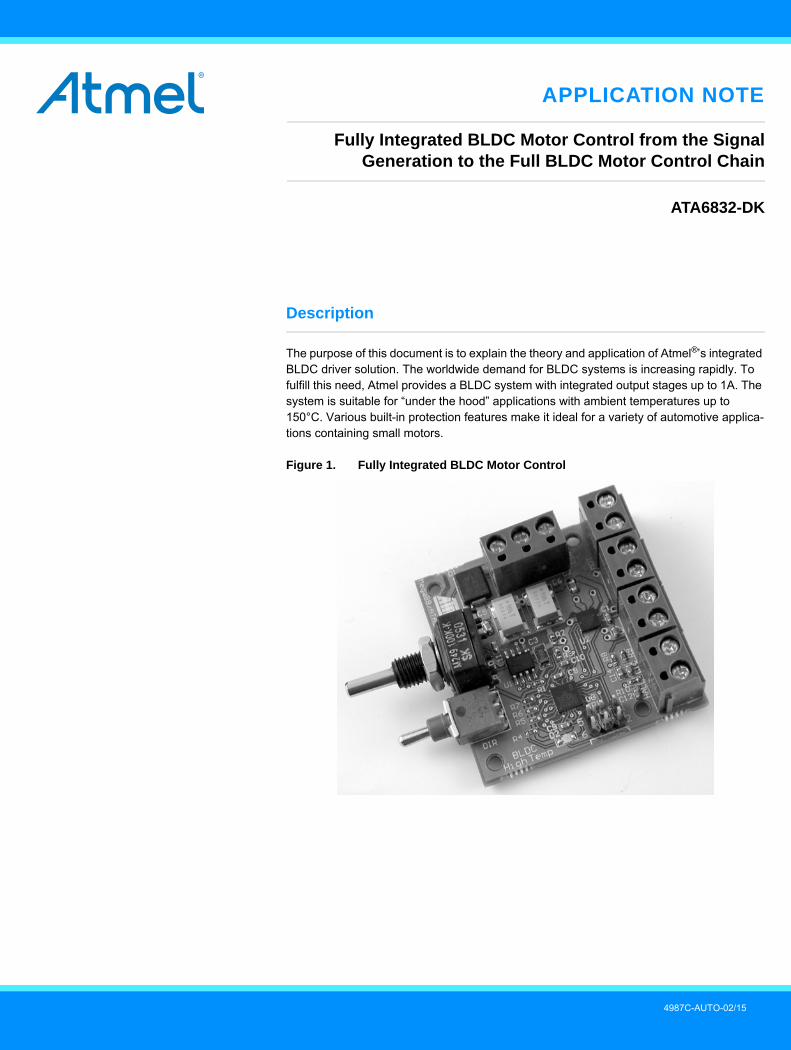
APPLICATION NOTE
Fully Integrated BLDC Motor Control from the SignalGeneration to the Full BLDC Motor Control Chain
ATA6832-DK
Description
The purpose of this document is to explain the theory and application of Atmel®’s integrated BLDC driver solution. The worldwide demand for BLDC systems is increasing rapidly. To fulfill this need, Atmel provides a BLDC system with integrated output stages up to 1A. The system is suitable for “under the hood” applications with ambient temperatures up to 150°C. Various built-in protection features make it ideal for a variety of automotive applica-tions containing small motors.
Figure 1. Fully Integrated BLDC Motor Control
4987C-AUTO-02/15
1. Fully Integrated BLDC System
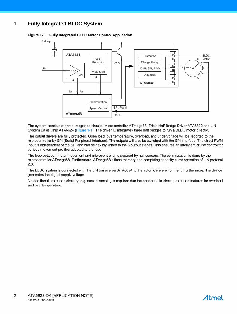
Figure 1-1. Fully Integrated BLDC Motor Control Application
The system consists of three integrated circuits: Microcontroller ATmega88, Triple Half Bridge Driver ATA6832 and LIN System Basis Chip ATA6624 (Figure 1-1). The driver IC integrates three half bridges to run a BLDC motor directly.
The output drivers are fully protected. Open load, overtemperature, overload, and undervoltage will be reported to the microcontroller by SPI (Serial Peripheral Interface). The outputs will also be switched with the SPI interface. The direct PWM input is independent of the SPI and can be flexibly linked to the 6 output stages. This ensures an intelligent cruise control for various movement profiles adapted to the load.
The loop between motor movement and microcontroller is assured by hall sensors. The commutation is done by the microcontroller ATmega88. Furthermore, ATmega88’s flash memory and computing capacity allow operation of LIN protocol 2.0.
The BLDC system is connected with the LIN transceiver ATA6624 to the automotive environment. Furthermore, this device generates the digital supply voltage.
No additional protection circuitry, e.g. current sensing is required due the enhanced in-circuit protection features for overload and overtemperature.
Protection
Diagnosis
BLDCMotor
W
U
VVCC
Battery
LIN
RxTx
SPI, PWM
HALL
Watchdog
Commutation
Speed Control
LIN
+
TRX
VCCRegulator
ATA6832
ATA6624
ATmega88
16 Bit SPI, PWM
Charge Pump
ATA6832-DK [APPLICATION NOTE]4987C–AUTO–02/15
2
2. Theory of BLDC Operation
Brushless DC motors are used in a growing number of applications as they offer several advantages, including reduced noise, long lifetime (no brush erosion), reduced noise, good weight/size to power ratio, and hazardous operation environment usability (with flammable products).
These types of motor have a little rotor inertia compared with other motor types. Coils are attached to the stator, and commutation is controlled by electronics using position sensors feedback or back electromotive force measurements.
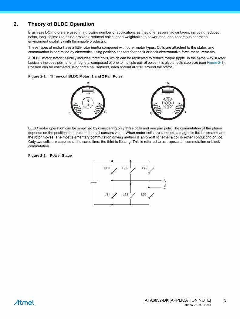
A BLDC motor stator basically includes three coils, which can be replicated to reduce torque ripple. In the same way, a rotor basically includes permanent magnets, composed of one to multiple pair of poles; this also affects step size (see Figure 2-1). Position can be estimated using three hall sensors, each spread at 120° around the stator.
Figure 2-1. Three-coil BLDC Motor, 1 and 2 Pair Poles
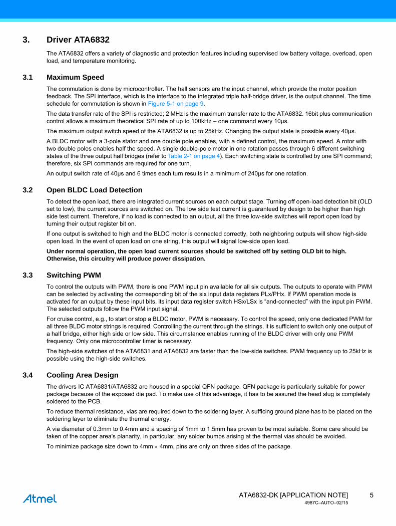
BLDC motor operation can be simplified by considering only three coils and one pair pole. The commutation of the phase depends on the position, in our case, the hall sensors value. When motor coils are supplied, a magnetic field is created and the rotor moves. The most elementary commutation driving method is an on-off scheme: a coil is either conducting or not. Only two coils are supplied at the same time; the third is floating. This is referred to as trapezoidal commutation or block commutation.
Figure 2-2. Power Stage
NS
A
BC
N
NS S
C B
A
BC
HS1 HS2
A
HS3
LS1 LS2 LS3
3ATA6832-DK [APPLICATION NOTE]4987C–AUTO–02/15
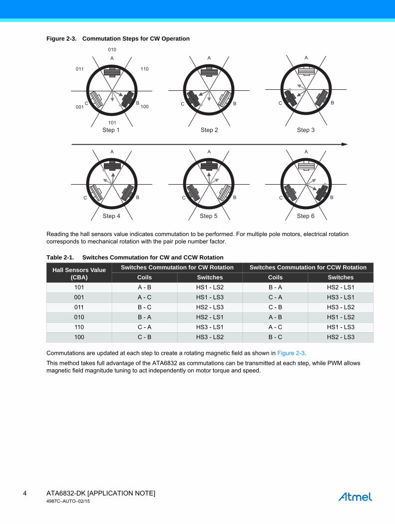
Figure 2-3. Commutation Steps for CW Operation
Reading the hall sensors value indicates commutation to be performed. For multiple pole motors, electrical rotation corresponds to mechanical rotation with the pair pole number factor.
Commutations are updated at each step to create a rotating magnetic field as shown in Figure 2-3.
This method takes full advantage of the ATA6832 as commutations can be transmitted at each step, while PWM allows magnetic field magnitude tuning to act independently on motor torque and speed.
Table 2-1. Switches Commutation for CW and CCW Rotation
Hall Sensors Value (CBA)
Switches Commutation for CW Rotation Switches Commutation for CCW Rotation
Coils Switches Coils Switches
101 A - B HS1 - LS2 B - A HS2 - LS1
001 A - C HS1 - LS3 C - A HS3 - LS1
011 B - C HS2 - LS3 C - B HS3 - LS2
010 B - A HS2 - LS1 A - B HS1 - LS2
110 C - A HS3 - LS1 A - C HS1 - LS3
100 C - B HS3 - LS2 B - C HS2 - LS3
A
BC
110
010
100
101
001
011
A
BC
A
BC
A
BC
A
BC
A
BC
Step 1 Step 2 Step 3
Step 4 Step 5 Step 6
ATA6832-DK [APPLICATION NOTE]4987C–AUTO–02/15
4
3. Driver ATA6832
The ATA6832 offers a variety of diagnostic and protection features including supervised low battery voltage, overload, open load, and temperature monitoring.
3.1 Maximum Speed
The commutation is done by microcontroller. The hall sensors are the input channel, which provide the motor position feedback. The SPI interface, which is the interface to the integrated triple half-bridge driver, is the output channel. The time schedule for commutation is shown in Figure 5-1 on page 9.
The data transfer rate of the SPI is restricted; 2 MHz is the maximum transfer rate to the ATA6832. 16bit plus communication control allows a maximum theoretical SPI rate of up to 100kHz – one command every 10µs.
The maximum output switch speed of the ATA6832 is up to 25kHz. Changing the output state is possible every 40µs.
A BLDC motor with a 3-pole stator and one double pole enables, with a defined control, the maximum speed. A rotor with two double poles enables half the speed. A single double-pole motor in one rotation passes through 6 different switching states of the three output half bridges (refer to Table 2-1 on page 4). Each switching state is controlled by one SPI command; therefore, six SPI commands are required for one turn.
An output switch rate of 40µs and 6 times each turn results in a minimum of 240µs for one rotation.
3.2 Open BLDC Load Detection
To detect the open load, there are integrated current sources on each output stage. Turning off open-load detection bit (OLD set to low), the current sources are switched on. The low side test current is guaranteed by design to be higher than high side test current. Therefore, if no load is connected to an output, all the three low-side switches will report open load by turning their output register bit on.
If one output is switched to high and the BLDC motor is connected correctly, both neighboring outputs will show high-side open load. In the event of open load on one string, this output will signal low-side open load.
Under normal operation, the open load current sources should be switched off by setting OLD bit to high. Otherwise, this circuitry will produce power dissipation.
3.3 Switching PWM
To control the outputs with PWM, there is one PWM input pin available for all six outputs. The outputs to operate with PWM can be selected by activating the corresponding bit of the six input data registers PLx/PHx. If PWM operation mode is activated for an output by these input bits, its input data register switch HSx/LSx is “and-connected” with the input pin PWM. The selected outputs follow the PWM input signal.
For cruise control, e.g., to start or stop a BLDC motor, PWM is necessary. To control the speed, only one dedicated PWM for all three BLDC motor strings is required. Controlling the current through the strings, it is sufficient to switch only one output of a half bridge, either high side or low side. This circumstance enables running of the BLDC driver with only one PWM frequency. Only one microcontroller timer is necessary.
The high-side switches of the ATA6831 and ATA6832 are faster than the low-side switches. PWM frequency up to 25kHz is possible using the high-side switches.
3.4 Cooling Area Design
The drivers IC ATA6831/ATA6832 are housed in a special QFN package. QFN package is particularly suitable for power package because of the exposed die pad. To make use of this advantage, it has to be assured the head slug is completely soldered to the PCB.
To reduce thermal resistance, vias are required down to the soldering layer. A sufficing ground plane has to be placed on the soldering layer to eliminate the thermal energy.
A via diameter of 0.3mm to 0.4mm and a spacing of 1mm to 1.5mm has proven to be most suitable. Some care should be taken of the copper area's planarity, in particular, any solder bumps arising at the thermal vias should be avoided.
To minimize package size down to 4mm 4mm, pins are only on three sides of the package.
5ATA6832-DK [APPLICATION NOTE]4987C–AUTO–02/15
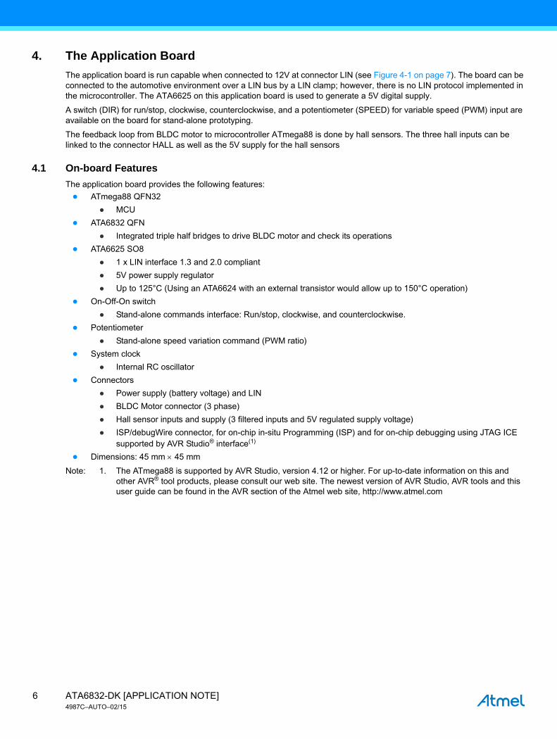
4. The Application Board
The application board is run capable when connected to 12V at connector LIN (see Figure 4-1 on page 7). The board can be connected to the automotive environment over a LIN bus by a LIN clamp; however, there is no LIN protocol implemented in the microcontroller. The ATA6625 on this application board is used to generate a 5V digital supply.
A switch (DIR) for run/stop, clockwise, counterclockwise, and a potentiometer (SPEED) for variable speed (PWM) input are available on the board for stand-alone prototyping.
The feedback loop from BLDC motor to microcontroller ATmega88 is done by hall sensors. The three hall inputs can be linked to the connector HALL as well as the 5V supply for the hall sensors
4.1 On-board Features
The application board provides the following features:
● ATmega88 QFN32
● MCU
● ATA6832 QFN
● Integrated triple half bridges to drive BLDC motor and check its operations
● ATA6625 SO8
● 1 x LIN interface 1.3 and 2.0 compliant
● 5V power supply regulator
● Up to 125°C (Using an ATA6624 with an external transistor would allow up to 150°C operation)
● On-Off-On switch
● Stand-alone commands interface: Run/stop, clockwise, and counterclockwise.
● Potentiometer
● Stand-alone speed variation command (PWM ratio)
● System clock
● Internal RC oscillator
● Connectors
● Power supply (battery voltage) and LIN
● BLDC Motor connector (3 phase)
● Hall sensor inputs and supply (3 filtered inputs and 5V regulated supply voltage)
● ISP/debugWire connector, for on-chip in-situ Programming (ISP) and for on-chip debugging using JTAG ICE supported by AVR Studio® interface(1)
● Dimensions: 45 mm 45 mm
Note: 1. The ATmega88 is supported by AVR Studio, version 4.12 or higher. For up-to-date information on this and other AVR® tool products, please consult our web site. The newest version of AVR Studio, AVR tools and this user guide can be found in the AVR section of the Atmel web site, http://www.atmel.com
ATA6832-DK [APPLICATION NOTE]4987C–AUTO–02/15
6
Figure 4-1. Application Board Top View and Connector Usage
4.2 High Ambient Temperature
The BLDC system is designed for high temperature environments. The MCU ATmega88 and the driver ATA6832 are qualified up to an ambient temperature of 150°C. The ATA6832 has enhanced temperature management; each of its output stages contains a thermal sensor. In addition to the thermal shutdown function, a thermal prewarning function is available. If the temperature exceeds the prewarning threshold, the microcontroller can react by reducing output power.
The SBC (system basis chip) ATA6625 is only qualified for junction temperatures up to 150°C. The power dissipation of its voltage regulator only allows for ambient temperature up to 125°C. ATA6624, a member of the same SBC family, allows operation with a discrete transistor for line regulation. Transistors are available for junction temperatures higher than 150°C. If such a line regulation transistor dissipates the heat, ATA6624’s temperature rise is only 3°C. Its possible ambient temperature is 147°C. Using a high temperature voltage regulator instead of Atmel’s SBC enables a full 150°C temperature range.
All discrete components used are enabled for temperatures up to 150°C.
Mounted connectors, a switch, and a potentiometer on the board, enable prototyping; however, these components are not high temperature qualified. The board can be integrated in hot temperature environment by wires.
Vbat
Speed
CCW
Stop
CW
Phase U
Phase V
Phase W
5V
Hall A
Hall B
Hall C
GND
LINPGND
1 23 45 6
JP1MISOSCKNRES
ISP MK2 Header
MOSI
GND
VCC 5V
7ATA6832-DK [APPLICATION NOTE]4987C–AUTO–02/15
5. Software Description
All code is implemented in C language, except SPI interrupt subroutine, which is implemented in assembly. Source code can be compiled using IAR® EWAVR 4.20A as well as AVR-GCC (WinAVR-20060421 with AVR Studio).
HTML documentation is included in the package. Use the High_temp_BLDC.html file in the root directory to start viewing the documentation.
Software behavior can be dispatched in three main working modes:
● Motor stopped
● In this mode, no hall sensors interrupts occurs. To maintain ATA6832 diagnostics, SPI communication is constantly performed by main loop.
● Command switch enables starting of the motor. A first frame has to be sent to the power driver to start the motor. This frame shall contain commutations to be applied according to motor position (hall sensors inputs) and to desired direction.
● While stopped, ATA6832 is switched into standby mode to decrease current consumption to lower than 20µA.
● Motor running
● Once the motor is started, SPI communications (commutations), are only handled by hall sensors ISR, each time an interrupt occurs.
● Command switch can be used to break the commutations evolution, and thus stop the motor.
● Degraded mode: two possibilities
● Motor has been stopped because of an overload, an over temperature, etc. Software waits for the user to clear the fault (operate switch to stop position).
● Motor is still running (software behavior is similar to the motor running mode). User is informed that a fault has been detected (over temperature, one or more switches are secured, etc.). Software can reduce output power and waits for a user order to clear the fault (operate switch to stop position).
5.1 Resources
The following MCU peripherals are used:
● SPI
● Commutation data and status data transfer to/from ATA6832 power driver
● Timer 1
● PWM generation through Output Compare 1A (OC1A pin)
● ADC channel 0
● Speed potentiometer value acquisition (Acts on PWM ratio)
● Pin change interrupts
● Hall sensor edges detection are used to detect motor position evolution
● I/O
● LED, Switch operations
● Optional (not managed by this stand-alone software)
● UART and Input Capture for LIN implementation
Table 5-1. Code, Data, and CPU Resources (Without Compiler Optimizations)
Compiler/Resources Code Size (Flash) Data Size (Ram) CPU Load
IAR EWAVR 4.20A 1 304bytes 367bytesSee §Schedule
AVR-GCC 1 826bytes 48bytes
ATA6832-DK [APPLICATION NOTE]4987C–AUTO–02/15
8
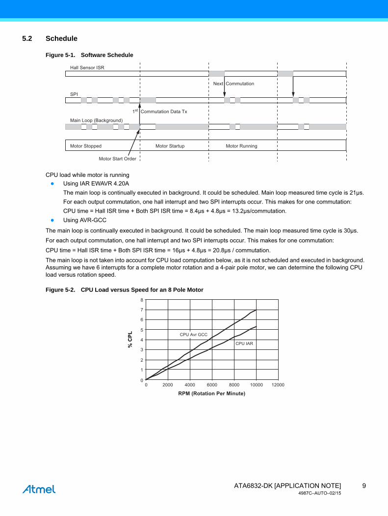
5.2 Schedule
Figure 5-1. Software Schedule
CPU load while motor is running
● Using IAR EWAVR 4.20A
The main loop is continually executed in background. It could be scheduled. Main loop measured time cycle is 21µs.
For each output commutation, one hall interrupt and two SPI interrupts occur. This makes for one commutation:
CPU time = Hall ISR time + Both SPI ISR time = 8.4µs + 4.8µs = 13.2µs/commutation.
● Using AVR-GCC
The main loop is continually executed in background. It could be scheduled. The main loop measured time cycle is 30µs.
For each output commutation, one hall interrupt and two SPI interrupts occur. This makes for one commutation:
CPU time = Hall ISR time + Both SPI ISR time = 16µs + 4.8µs = 20.8µs / commutation.
The main loop is not taken into account for CPU load computation below, as it is not scheduled and executed in background. Assuming we have 6 interrupts for a complete motor rotation and a 4-pair pole motor, we can determine the following CPU load versus rotation speed.
Figure 5-2. CPU Load versus Speed for an 8 Pole Motor
Hall Sensor ISR
Main Loop (Background)
SPI
Motor Stopped Motor Startup
Motor Start Order
Commutation Data Tx
CommutationNext
1st
Motor Running
0 2000 4000 6000 8000 10000 12000
RPM (Rotation Per Minute)
5
4
3
2
8
7
6
1
0
% C
PL CPU Avr GCC
CPU IAR
9ATA6832-DK [APPLICATION NOTE]4987C–AUTO–02/15
5.3 Diagrams
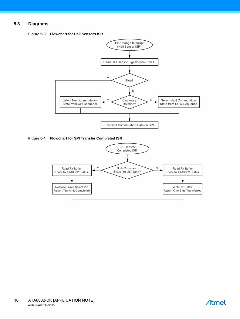
Figure 5-3. Flowchart for Hall Sensors ISR
Figure 5-4. Flowchart for SPI Transfer Completed ISR
ClockwiseRotation?
Read Hall Sensor Signals from Port C
Select Next CommutationState from CW Sequence
Pin Change Interrupt(Hall Sensor ISR)
Stop?Y
N
Y N
Transmit Commutation Data on SPI
Select Next CommutationState from CCW Sequence
Read Rx BufferStore to ATA6832 Status
Read Rx BufferStore to ATA6832 Status
SPI TransmitCompleted ISR
Both CommandBytes (16 bits) Sent?
Y N
Release Slave Select PinReport Transmit Completed
Write Tx BufferReport One Byte Transferred
ATA6832-DK [APPLICATION NOTE]4987C–AUTO–02/15
10
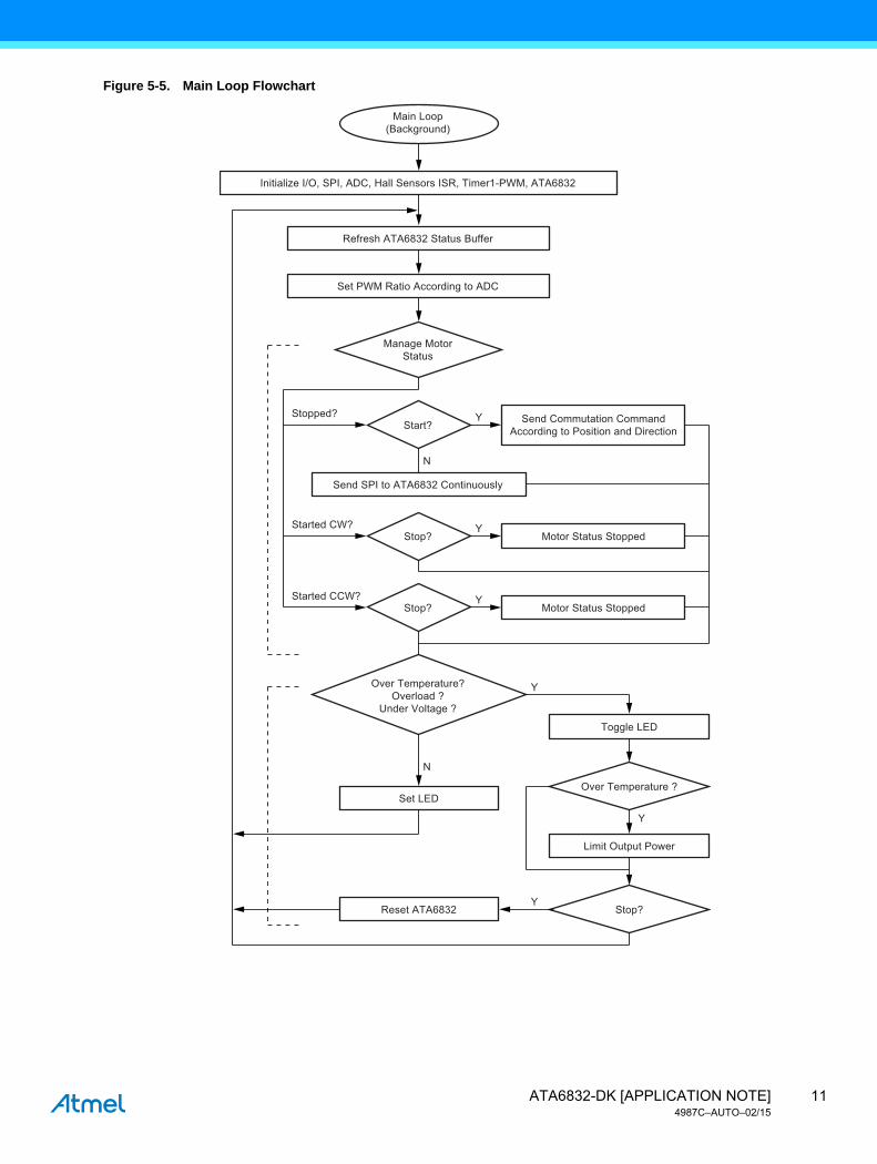
Figure 5-5. Main Loop Flowchart
Over Temperature?Overload ?
Under Voltage ?
Manage MotorStatus
Main Loop(Background)
Stop?
Start?Stopped?
N
N
Y
Initialize I/O, SPI, ADC, Hall Sensors ISR, Timer1-PWM, ATA6832
Set PWM Ratio According to ADC
Motor Status Stopped
Send SPI to ATA6832 Continuously
Refresh ATA6832 Status Buffer
Send Commutation CommandAccording to Position and Direction
Started CW? Y
Stop? Motor Status Stopped
Limit Output Power
Toggle LED
Over Temperature ?
Stop?Reset ATA6832
Set LED
Started CCW?
Y
Y
Y
Y
11ATA6832-DK [APPLICATION NOTE]4987C–AUTO–02/15
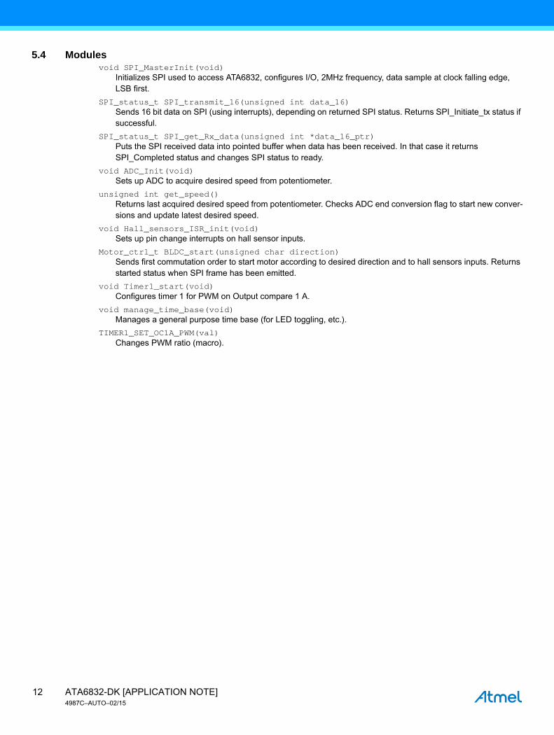
5.4 Modules void SPI_MasterInit(void)
Initializes SPI used to access ATA6832, configures I/O, 2MHz frequency, data sample at clock falling edge, LSB first.
SPI_status_t SPI_transmit_16(unsigned int data_16)Sends 16 bit data on SPI (using interrupts), depending on returned SPI status. Returns SPI_Initiate_tx status if successful.
SPI_status_t SPI_get_Rx_data(unsigned int *data_16_ptr)Puts the SPI received data into pointed buffer when data has been received. In that case it returns SPI_Completed status and changes SPI status to ready.
void ADC_Init(void)Sets up ADC to acquire desired speed from potentiometer.
unsigned int get_speed()Returns last acquired desired speed from potentiometer. Checks ADC end conversion flag to start new conver-sions and update latest desired speed.
void Hall_sensors_ISR_init(void)Sets up pin change interrupts on hall sensor inputs.
Motor_ctrl_t BLDC_start(unsigned char direction)Sends first commutation order to start motor according to desired direction and to hall sensors inputs. Returns started status when SPI frame has been emitted.
void Timer1_start(void)Configures timer 1 for PWM on Output compare 1 A.
void manage_time_base(void)Manages a general purpose time base (for LED toggling, etc.).
TIMER1_SET_OC1A_PWM(val)Changes PWM ratio (macro).
ATA6832-DK [APPLICATION NOTE]4987C–AUTO–02/15
12
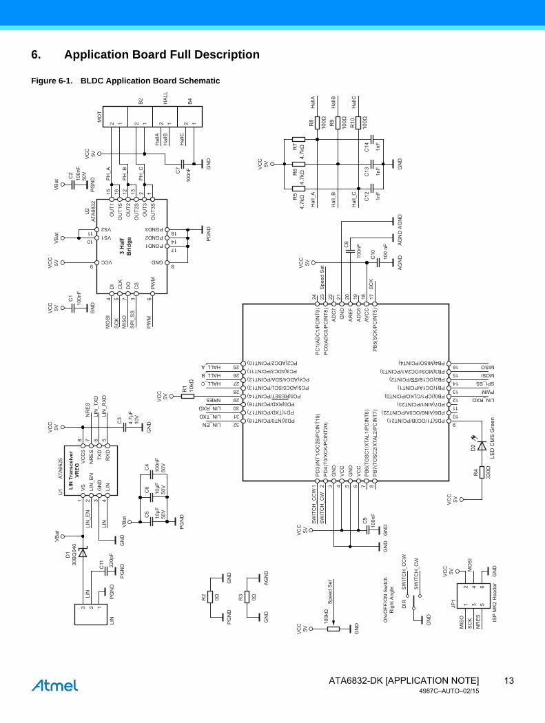
6. Application Board Full Description
Figure 6-1. BLDC Application Board Schematic
Hal
lC
Hal
lB
Hal
lA
Hal
l_C
R10
100Ω
SP
I_S
SM
ISO
1
PD2(INT0/PCINT18)PD1(TXD/PCINT17)PD0(RXD/PCINT16)
PC5(ADC5/SCL/PCINT13)
PC2(ADC2/PCINT10)PC3(ADC3/PCINT11)
PC4(ADC4/SDA/PCINT12)
PC6(RESET/PCINT14)
PD5(T1/OC0B/PCINT21)32
9
1011
8
1714
31302928272625
VS1VS2
VCC
PGND2PGND3
PGND1
GND
LIN_ENLIN_TXDLIN_RXD
LIN_RXDPWMSPI_SSMOSIMISO
NRES
HALL_CHALL_BHALL_A
910111213141516
PD6(AIN0/OC0A/PCINT22)PD7(AIN1/PCINT23)PB0(ICP1/CLKO/PCINT0)
PB1(OC1A/PCINT1)PB2(OC1B/SS/PCINT2)
PB4(MISO/PCINT4)
PB3(MOSI/OC2A1/PCINT3)
VS
U1
ATA
6625
U2
ATA
6832
PD
3(IN
T1/O
C2B
/PC
INT1
9)
GN
D
AG
ND
GN
D
GN
D
GN
D
GN
DP
GN
D
LIN
AG
ND
GN
D
MO
SI
ISP
MK
2 H
eade
r
MIS
OJP
1
NR
ES
SC
K
DIR
VC
C5V
VC
C5V
VC
C5V
VC
C5V
100n
FC
910μF
50V
4.7μ
F10
V
C5
C3
C11
100k
Ω
0ΩR3
10kΩ
R1
4.7k
ΩR5
4.7k
ΩR6
4.7k
ΩR7
R8
100Ω
2
SW
ITC
H_C
CW
ON
/OFF
/ON
Sw
itch
Rig
ht A
ngle S
WIT
CH
_CW
SW
ITC
H_C
CW
8 7 6 5
NR
ES
LIN
_TX
DLI
N_R
XD
13
Spe
ed S
etS
WIT
CH
_CW
PD
4(T0
/XC
K/P
CIN
T20)
3G
ND
VC
C5V
4V
CC
5G
ND
8P
B7(
TOS
C2/
XTA
L2/P
CIN
T7)
7P
B6(
TOS
C1/
XTA
L1/P
CIN
T6)
6
24 23
SC
K
Spe
ed S
et22 21 20 171819
VC
C
PC
1(A
DC
1/P
CIN
T9)
PC
0(A
DC
0/P
CIN
T8)
AD
C7
GN
D
AR
EF
PB
5(S
CK
/PC
INT5
)AV
CC
AD
C6
PG
ND
VB
at
VB
at
30B
Q04
0D
1
GN
D
PG
ND
3 H
alf
Brid
ge
GN
D
GN
D
PG
ND
10μF
50V
C6
100n
F50
V
100n
F50
V
220p
F
C1
100n
F
C7
100n
F
C12 1nF
C4
PG
ND
GN
D
LIN
Tra
nsce
iver
VREG
0ΩR2
LIN
_EN
2LI
N_E
NLI
N
GN
D3
LIN
VC
C5
NR
ES
TXD
RX
D4
LIN
OU
T1O
UT1
SO
UT2
OU
T2S
OU
T3O
UT3
S
DI
PH
_A
PH
_B
PH
_C
15
2 1
Hal
lA
Hal
l_B
Hal
l_A
Hal
lC
Hal
lB2 12 12
B4
HA
LL
B2
116 12 13 1
4
CLK
5
MO
SI
SC
K
DO
7
CS
3
PW
MP
WM
6
18
12
12 1 532
GN
D
64
VC
C5V
VC
C5V
MO
T
VC
C5V
VB
atV
Bat
VC
C5V
100
nF
100n
F
C10
C8 AG
ND
GN
DA
GN
D
VC
C5V
PG
NDC
2
VC
C5V
R9
100Ω
R4
LED
CM
S G
reen
D2
330Ω
C13 1nF
C14 1nF
13ATA6832-DK [APPLICATION NOTE]4987C–AUTO–02/15
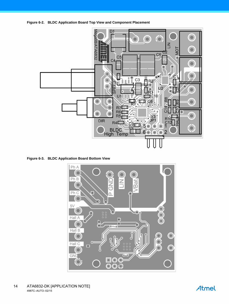
Figure 6-2. BLDC Application Board Top View and Component Placement
Figure 6-3. BLDC Application Board Bottom View
ATA6832-DK [APPLICATION NOTE]4987C–AUTO–02/15
14
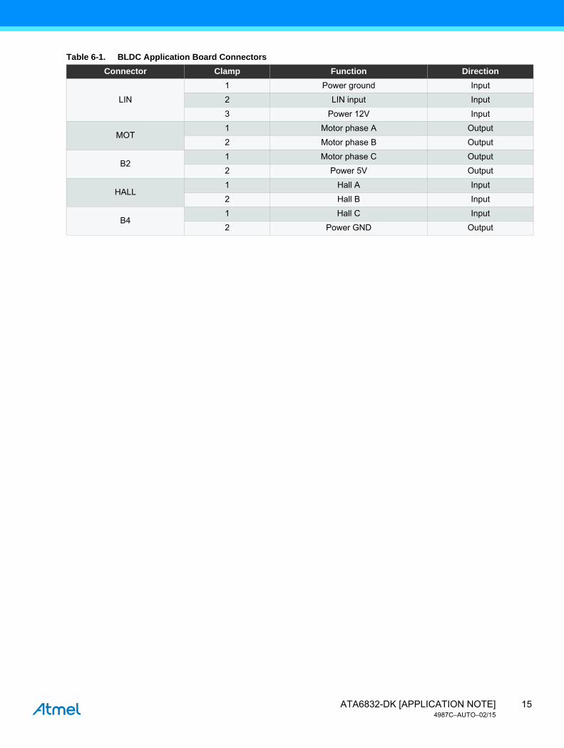
Table 6-1. BLDC Application Board Connectors
Connector Clamp Function Direction
LIN
1 Power ground Input
2 LIN input Input
3 Power 12V Input
MOT1 Motor phase A Output
2 Motor phase B Output
B21 Motor phase C Output
2 Power 5V Output
HALL1 Hall A Input
2 Hall B Input
B41 Hall C Input
2 Power GND Output
15ATA6832-DK [APPLICATION NOTE]4987C–AUTO–02/15

7. Revision History
Please note that the following page numbers referred to in this section refer to the specific revision mentioned, not to this document.
Revision No. History
4987C-AUTO-02/15 Put document in the latest template
ATA6832-DK [APPLICATION NOTE]4987C–AUTO–02/15
16
XX X XX XAtmel Corporation 1600 Technology Drive, San Jose, CA 95110 USA T: (+1)(408) 441.0311 F: (+1)(408) 436.4200 | www.atmel.com
© 2015 Atmel Corporation. / Rev.: 4987C–AUTO–02/15
Atmel®, Atmel logo and combinations thereof, Enabling Unlimited Possibilities®, AVR®, AVR Studio®, and others are registered trademarks or trademarks of Atmel Corporation in U.S. and other countries. Other terms and product names may be trademarks of others.
DISCLAIMER: The information in this document is provided in connection with Atmel products. No license, express or implied, by estoppel or otherwise, to any intellectual property rightis granted by this document or in connection with the sale of Atmel products. EXCEPT AS SET FORTH IN THE ATMEL TERMS AND CONDITIONS OF SALES LOCATED ON THEATMEL WEBSITE, ATMEL ASSUMES NO LIABILITY WHATSOEVER AND DISCLAIMS ANY EXPRESS, IMPLIED OR STATUTORY WARRANTY RELATING TO ITS PRODUCTSINCLUDING, BUT NOT LIMITED TO, THE IMPLIED WARRANTY OF MERCHANTABILITY, FITNESS FOR A PARTICULAR PURPOSE, OR NON-INFRINGEMENT. IN NO EVENTSHALL ATMEL BE LIABLE FOR ANY DIRECT, INDIRECT, CONSEQUENTIAL, PUNITIVE, SPECIAL OR INCIDENTAL DAMAGES (INCLUDING, WITHOUT LIMITATION, DAMAGESFOR LOSS AND PROFITS, BUSINESS INTERRUPTION, OR LOSS OF INFORMATION) ARISING OUT OF THE USE OR INABILITY TO USE THIS DOCUMENT, EVEN IF ATMEL HASBEEN ADVISED OF THE POSSIBILITY OF SUCH DAMAGES. Atmel makes no representations or warranties with respect to the accuracy or completeness of the contents of thisdocument and reserves the right to make changes to specifications and products descriptions at any time without notice. Atmel does not make any commitment to update the informationcontained herein. Unless specifically provided otherwise, Atmel products are not suitable for, and shall not be used in, automotive applications. Atmel products are not intended,authorized, or warranted for use as components in applications intended to support or sustain life.
SAFETY-CRITICAL, MILITARY, AND AUTOMOTIVE APPLICATIONS DISCLAIMER: Atmel products are not designed for and will not be used in connection with any applications wherethe failure of such products would reasonably be expected to result in significant personal injury or death (“Safety-Critical Applications”) without an Atmel officer's specific writtenconsent. Safety-Critical Applications include, without limitation, life support devices and systems, equipment or systems for the operation of nuclear facilities and weapons systems.Atmel products are not designed nor intended for use in military or aerospace applications or environments unless specifically designated by Atmel as military-grade. Atmel products arenot designed nor intended for use in automotive applications unless specifically designated by Atmel as automotive-grade.