Embed Size (px)
Citation preview
consumption, whilst retaining a high
level of performance, in particular
through the use of copper interconnects
and low-k dielectrics. To fully utilise
these advantages, special features,
such as enhanced support for
RFCMOS and power-reduction design
methodology, are available for selected
technologies.
FACTSHEETASIC/FOUNDRY TECHNOLOGY
� European Design Centres in Langen
near Frankfurt and Munich
� Dedicated Mixed Signal Design
Team in Maidenhead
� Triple Well and RF process options
available
� SoC design expertise
� Large IP portfolio (silicon proven)
� Packaging technology supports
designs from low pin count
(FBGA/QFP) to high pin count
(FCBGA) packages with up to
2100 balls
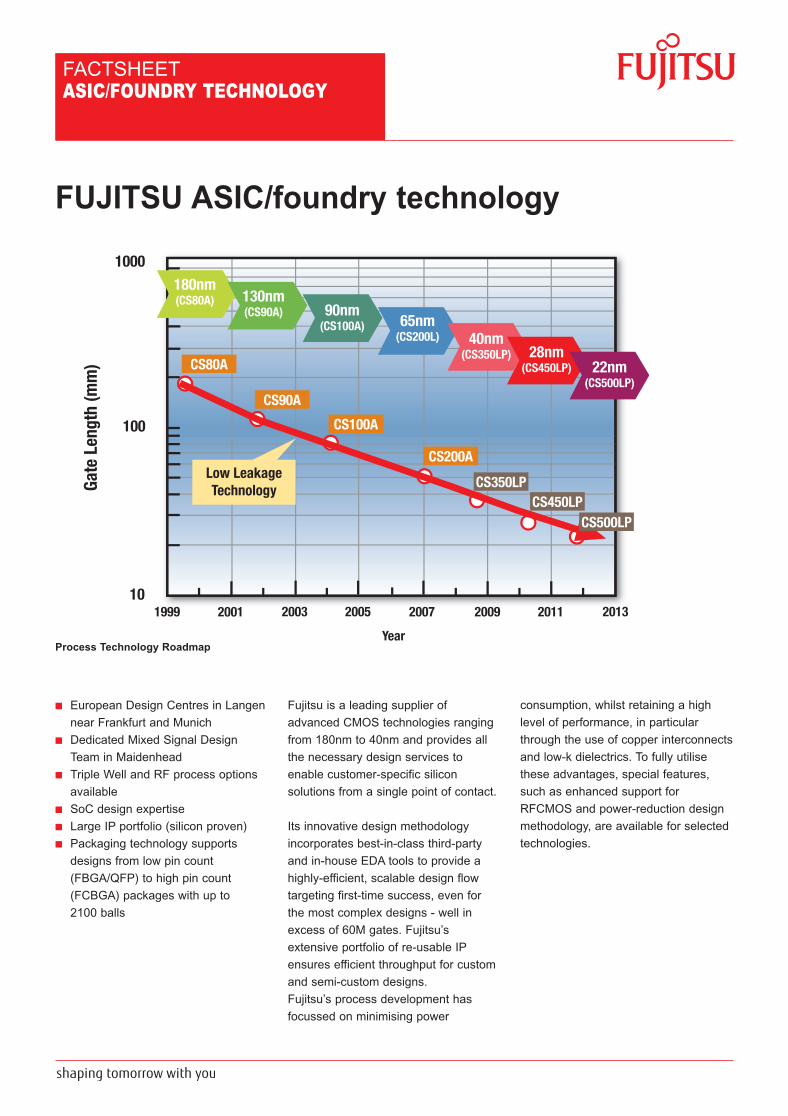
FUJITSU ASIC/foundry technology
Fujitsu is a leading supplier of
advanced CMOS technologies ranging
from 180nm to 40nm and provides all
the necessary design services to
enable customer-specific silicon
solutions from a single point of contact.
Its innovative design methodology
incorporates best-in-class third-party
and in-house EDA tools to provide a
highly-efficient, scalable design flow
targeting first-time success, even for
the most complex designs - well in
excess of 60M gates. Fujitsu’s
extensive portfolio of re-usable IP
ensures efficient throughput for custom
and semi-custom designs.
Fujitsu’s process development has
focussed on minimising power
1000
100
10
Year
Gate
Leng
th(m
m)
1999 2001 2003 2005 2007 2009 2011 2013
CS350LPCS450LP
CS500LP
CS200A
CS100A
CS90A
CS80A
180nm(CS80A) 130nm
(CS90A) 90nm(CS100A) 65nm
(CS200L) 40nm(CS350LP) 28nm
(CS450LP) 22nm(CS500LP)
Low LeakageTechnology
Process Technology Roadmap
ASIC Foundry Factsheet:ASIC Foundry Factsheet 15/9/10 16:24 Page 1
2
FACTSHEETASIC/FOUNDRY TECHNOLOGY
FSEU-C50-06SEP10
ASK FUJITSU SEMICONDUCTOR EUROPE
Contact us on +49(0) 61 03 69 00 or visithttp://emea.fujitsu.com/asic
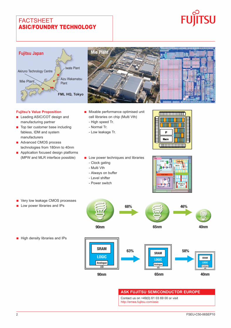
Fujitsu’s Value Proposition
� Leading ASIC/COT design and
manufacturing partner
� Top tier customer base including
fabless, IDM and system
manufacturers
� Advanced CMOS process
technologies from 180nm to 40nm
� Application focused design platforms
(MPW and MLR interface possible)
� Very low leakage CMOS processes
� Low power libraries and IPs
� Mixable performance optimised unit
cell libraries on chip (Multi Vth)
- High speed Tr.
- Normal Tr.
- Low leakage Tr.
90nm 65nm 40nm
68% 46%
� Low power techniques and libraries
- Clock gating
- Multi Vth
- Always on buffer
- Level shifter
- Power switch
Mie PlantFujitsu Japan
Akiruno Technology Centre
Mie Plant
Iwate Plant
Aizu WakamatsuPlant
FML HQ, Tokyo
SRAM
LOGICAnalogue
I/O
SRAM
LOGICAnalogue
I/O
SRAM
LOGICAnalogue
I/O
90nm 65nm 40nm
63% 58%
� High density libraries and IPs
ASIC Foundry Factsheet:ASIC Foundry Factsheet 15/9/10 16:24 Page 2