Embed Size (px)
Citation preview
© 2
FSQ0365, FSQ
0265, FSQ0165, FSQ
321, FSQ311 —
Green M
ode Fairchild Power Sw
itch (FPS™)
FSQ
September 2007
FPSTM is a trademark of Fairchild Semiconductor Corporation.
FSQ0365, FSQ0265, FSQ0165, FSQ321, FSQ311Green Mode Fairchild Power Switch (FPS™) forValley Switching Converter - Low EMI and High Efficiency
FeaturesOptimized for Valley Switching (VSC)Low EMI through Variable Frequency Control and Inherent Frequency ModulationHigh-Efficiency through Minimum Voltage SwitchingNarrow Frequency Variation Range over Wide Load and Input Voltage VariationAdvanced Burst-Mode Operation for Low Standby Power ConsumptionPulse-by-Pulse Current Limit Various Protection Functions: Overload Protection (OLP), Over-Voltage Protection (OVP), Abnormal Over-Current Protection (AOCP), Internal Thermal Shutdown (TSD) Under-Voltage Lockout (UVLO) with HysteresisInternal Start-up Circuit Internal High-Voltage SenseFET (650V)Built-in Soft-Start (15ms)
ApplicationsPower Supply for DVP Player and DVD Recorder,Set-Top BoxAdapterAuxiliary Power Supply for PC, LCD TV, and PDP TV
Related Application NotesAN-4137, AN-4141, AN-4147, AN-4150 (Flyback)AN-4134 (Forward)
DescriptionA Valley Switching Converter generally shows lower EMIand higher power conversion efficiency than aconventional hard-switched converter with a fixedswitching frequency. The FSQ-series is an integratedPulse-Width Modulation (PWM) controller andSenseFET specifically designed for valley switchingoperation with minimal external components. The PWMcontroller includes an integrated fixed-frequencyoscillator, Under-Voltage Lockout, Leading EdgeBlanking (LEB), optimized gate driver, internal soft-start,temperature-compensated precise current sources forloop compensation, and self-protection circuitry.
Compared with discrete MOSFET and PWM controllersolutions, the FSQ-series reduces total cost, componentcount, size and weight; while simultaneously increasingefficiency, productivity, and system reliability. This deviceprovides a basic platform that is well suited for cost-effective designs of valley switching fly-back converters.
006 Fairchild Semiconductor Corporation www.fairchildsemi.com0365, FSQ0265, FSQ0165, FSQ321, FSQ311 Rev. 1.0.5
FSQ0365, FSQ
0265, FSQ0165, FSQ
321, FSQ311 —
Green M
ode Fairchild Power Sw
itch (FPS™)
© 2FSQ
Ordering Information
Notes:1. The junction temperature can limit the maximum output power. 2. 230VAC or 100/115VAC with doubler. The maximum power with CCM operation.3. Typical continuous power in a non-ventilated enclosed adapter measured at 50°C ambient temperature. 4. Maximum practical continuous power in an open-frame design at 50°C ambient.5. Pb-free package per JEDEC J-STD-020B.
Product Number(5) PKG. Operating
Temp.
Cur-rent Limit
RDS(ON) Max.
Maximum Output Power(1)
ReplacesDevices230VAC±15%(2) 85-265VAC
Adapter(3) Open-Frame(4) Adapter(3) Open-Frame(4)
FSQ311 8-DIP-40 to +85C 0.6A 19Ω 7W 10W 6W 8W FSDL321
FSDM311FSQ311L 8-LSOP
FSQ321 8-DIP-40 to +85°C 0.6A 19Ω 8W 12W 7W 10W FSDL321
FSDM311FSQ321L 8-LSOP
FSQ0165RN 8-DIP-40 to +85°C 0.9A 10Ω 10W 15W 9W 13W FSDL0165RN
FSQ0165RL 8-LSOP
FSQ0265RN 8-DIP-40 to +85°C 1.2A 6Ω 14W 20W 11W 16W FSDM0265RN
FSDM0265RNB FSQ0265RL 8-LSOP
FSQ0365RN 8-DIP-40 to +85°C 1.5A 4.5Ω 17.5W 25W 13W 19W FSDM0365RN
FSDM0365RNBFSQ0365RL 8-LSOP
006 Fairchild Semiconductor Corporation www.fairchildsemi.com0365, FSQ0265, FSQ0165, FSQ321, FSQ311 Rev. 1.0.5 2
FSQ0365, FSQ
0265, FSQ0165, FSQ
321, FSQ311 —
Green M
ode Fairchild Power Sw
itch (FPS™)
© 2FSQ
Typical Circuit
Figure 1. Typical Flyback Application
Internal Block Diagram
Figure 2. Functional Block Diagram
Vcc
GND
Drain
Sync
VO
PWM
Vfb
AC IN
Vstr
FSQ0365RN Rev.00
8V/12V
Vref
S
Q
Q
R
VCC Vref
Idelay IFB
VSD
Vovp
Sync
VOCPS
Q
Q
R
R
3R
VCC good
Vcc Drain
Vfb
GND
AOCP
Gate driver
VCC good
LEB200ns
PWM
VBurst
4Sync
+
-
+
-0.7V/0.2V
2.5μs time delay
(1.1V)
Soft- Start
6V
6V
0.35/0.55+
-
OSC
Vstr
TSD
3
2 8765
FSQ0365RN Rev.00
1
006 Fairchild Semiconductor Corporation www.fairchildsemi.com0365, FSQ0265, FSQ0165, FSQ321, FSQ311 Rev. 1.0.5 3
FSQ0365, FSQ
0265, FSQ0165, FSQ
321, FSQ311 —
Green M
ode Fairchild Power Sw
itch (FPS™)
© 2FSQ
Pin Configuration
Figure 3. Pin Configuration (Top View)
Pin DefinitionsPin # Name Description
1 GND SenseFET source terminal on primary side and internal control ground.
2 Vcc
Positive supply voltage input. Although connected to an auxiliary transformer winding, current is supplied from pin 5 (Vstr) via an internal switch during startup (see Internal Block Diagram Section). It is not until VCC reaches the UVLO upper threshold (12V) that the internal start-up switch opens and device power is supplied via the auxiliary transformer winding.
3 Vfb
The feedback voltage pin is the non-inverting input to the PWM comparator. It has a 0.9mA current source connected internally while a capacitor and optocoupler are typically connected externally. There is a time delay while charging external capacitor Cfb from 3V to 6V using an internal 5μA current source. This time delay prevents false triggering under transient condi-tions but still allows the protection mechanism to operate under true overload conditions.
4 Sync
This pin is internally connected to the sync-detect comparator for valley switching. Typically the voltage of the auxiliary winding is used as Sync input voltage and external resistors and capac-itor are needed to make time delay to match valley point. The threshold of the internal sync comparator is 0.7V/0.2V.
5 VstrThis pin is connected to the rectified AC line voltage source. At start-up the internal switch sup-plies internal bias and charges an external storage capacitor placed between the Vcc pin and ground. Once the Vcc reaches 12V, the internal switch is opened.
6,7,8 DrainThe drain pins are designed to connect directly to the primary lead of the transformer and are capable of switching a maximum of 700V. Minimizing the length of the trace connecting these pins to the transformer will decrease leakage inductance.
GND
Vcc
Sync Vstr
8-DIP
Vfb
D
D
D
FSQ0365RN Rev.01
8-LSOPV
006 Fairchild Semiconductor Corporation www.fairchildsemi.com0365, FSQ0265, FSQ0165, FSQ321, FSQ311 Rev. 1.0.5 4
FSQ0365, FSQ
0265, FSQ0165, FSQ
321, FSQ311 —
Green M
ode Fairchild Power Sw
itch (FPS™)
© 2FSQ
Absolute Maximum RatingsStresses exceeding the absolute maximum ratings may damage the device. The device may not function or be opera-ble above the recommended operating conditions and stressing the parts to these levels is not recommended. In addi-tion, extended exposure to stresses above the recommended operating conditions may affect device reliability. Theabsolute maximum ratings are stress ratings only. TA = 25°C, unless otherwise specified.
Notes:6. Repetitive rating: Pulse width limited by maximum junction temperature.7. L=51mH, starting TJ=25°C.8. Meets JEDEC standards JESD22-A114 and JESD22-A115.
Thermal Impedance
Notes: 9. All items are tested with the standards JESD 51-2 and 51-10 (DIP).10. Free-standing, with no heat-sink, under natural convection.11. Infinite cooling condition - refer to the SEMI G30-88.12. Measured on the package top surface.
Symbol Characteristic Min. Max. UnitVSTR Vstr Pin Voltage 500 V
VDS Drain Pin Voltage 650 V
VCC Supply Voltage 20 V
VFB Feedback Voltage Range -0.3 9.0 V
VSync Sync Pin Voltage Range -0.3 9.0 V
IDM Drain Current Pulsed(6)
FSQ0365 12
AFSQ0265 8
FSQ0165 4
FSQ321/311 1.5
EAS Single Pulsed Avalanche Energy(7)
FSQ0365 230
mJFSQ0265 140
FSQ0165 50
FSQ321/311 10
PD Total Power Dissipation 1.5 W
TJ Recommended Operating Junction Temperature -40 Internally limited °C
TA Operating Ambient Temperature -40 85 °C
TSTG Storage Temperature -55 150 °C
ESD Human Body Model(8) CLASS1 C
Machine Model(8) CLASS B
Symbol Parameter Value Unit8-DIP(9)
θJA(10) Junction-to-Ambient Thermal Resistance 80
°C/WθJC(11) Junction-to-Case Thermal Resistance 20
θJT(12) Junction-to-Top Thermal Resistance 35
006 Fairchild Semiconductor Corporation www.fairchildsemi.com0365, FSQ0265, FSQ0165, FSQ321, FSQ311 Rev. 1.0.5 5
FSQ0365, FSQ
0265, FSQ0165, FSQ
321, FSQ311 —
Green M
ode Fairchild Power Sw
itch (FPS™)
© 2FSQ
Electrical Characteristics TA = 25°C unless otherwise specified.
Symbol Parameter Condition Min. Typ. Max. Unit SenseFET Section
BVDSS Drain Source Breakdown Voltage VCC = 0V, ID = 100µA 650 VIDSS Zero-Gate-Voltage Drain Current VDS = 560V 100 µA
RDS(ON)Drain-Source On-State Resistance(13)
FSQ0365
TJ = 25°C, ID = 0.5A
3.5 4.5
ΩFSQ0265 5.0 6.0FSQ0165 8.0 10.0
FSQ321/311 14.0 19.0
CSS Input Capacitance
FSQ0365
VGS = 0V, VDS = 25V, f = 1MHz
315
pFFSQ0265 550FSQ0165 250
FSQ321/311 162
COSS Output Capacitance
FSQ0365
VGS = 0V, VDS = 25V, f = 1MHz
47
pFFSQ0265 38FSQ0165 25
FSQ321/311 18
CRSSReverse Transfer Capacitance
FSQ0365
VGS = 0V, VDS = 25V, f = 1MHz
9.0
pFFSQ0265 17.0FSQ0165 10.0
FSQ321/311 3.8
td(on) Turn-On Delay Time
FSQ0365
VDD = 350V, ID = 25mA
11.2
nsFSQ0265 20.0FSQ0165 12.0
FSQ321/311 9.5
tr Rise Time
FSQ0365
VDD = 350V, ID = 25mA
34
nsFSQ0265 15FSQ0165 4
FSQ321/311 19
td(off) Turn-Off Delay Time
FSQ0365
VDD = 350V, ID = 25mA
28.2
nsFSQ0265 55.0FSQ0165 30.0
FSQ321/311 33.0
tf Fall Time
FSQ0365
VDD = 350V, ID = 25mA
32
nsFSQ0265 25FSQ0165 10
FSQ321/311 42Control SectiontON.MAX1 Maximum On Time1 All but Q321 TJ = 25°C 10.5 12.0 13.5 µstON.MAX2 Maximum On Time2 Q321 TJ = 25°C 6.35 7.06 7.77 µs
tB1 Blanking Time1 All but Q321 13.2 15.0 16.8 µstB2 Blanking Time2 Q321 7.5 8.2 µs
006 Fairchild Semiconductor Corporation www.fairchildsemi.com0365, FSQ0265, FSQ0165, FSQ321, FSQ311 Rev. 1.0.5 6
FSQ0365, FSQ
0265, FSQ0165, FSQ
321, FSQ311 —
Green M
ode Fairchild Power Sw
itch (FPS™)
© 2FSQ
Electrical Characteristics (Continued)
TA = 25°C unless otherwise specified.
Notes:13. Pulse test: Pulse-Width=300μs, duty=2%14. Though guaranteed, it is not 100% tested in production.15. Propagation delay in the control IC.16. Includes gate turn-on time.
Symbol Parameter Condition Min. Typ. Max. Unit tW Detection Time Window TJ = 25°C, Vsync = 0V 3.0 µsfS1 Initial Switching Freq.1 All but Q321 50.5 55.6 61.7 kHzfS2 Initial Switching Freq.2 Q321 84.0 89.3 95.2 kHzΔfS Switching Frequency Variation(14) -25°C < TJ < 85°C ±5 ±10 %IFB Feedback Source Current VFB = 0V 700 900 1100 µA
DMIN Minimum Duty Cycle VFB = 0V 0 %VSTART UVLO Threshold Voltage After turn-on
11 12 13 VVSTOP 7 8 9 VtS/S1 Internal Soft-Start Time1 All but Q321 With free-running frequency 15 mstS/S2 Internal Soft-Start Time2 Q321 With free-running frequency 10 ms
Burst Mode SectionVBURH
Burst-Mode Voltage TJ = 25°C, tPD = 200ns(15)0.45 0.55 0.65 V
VBURL 0.25 0.35 0.45 VVBUR(HYS) 200 mVProtection Section
ILIM Peak Current Limit
FSQ0365 TJ = 25°C, di/dt = 240mA/µs 1.32 1.50 1.68
AFSQ0265 TJ = 25°C, di/dt = 200mA/µs 1.06 1.20 1.34FSQ0165 TJ = 25°C, di/dt = 175mA/µs 0.8 0.9 1.0FSQ321 TJ = 25°C, di/dt = 125mA/µs 0.53 0.60 0.67FSQ311 TJ = 25°C, di/dt = 112mA/µs 0.53 0.60 0.67
VSD Shutdown Feedback Voltage VCC = 15V 5.5 6.0 6.5 VIDELAY Shutdown Delay Current VFB = 5V 4 5 6 µAtLEB Leading-Edge Blanking Time(14) 200 ns
VOVP Over-Voltage Protection VCC = 15V, VFB = 2V 5.5 6.0 6.5 VtOVP Over-Voltage Protection Blanking Time 2 3 4 µsTSD Thermal Shutdown Temperature(14) 125 140 155 °C
Sync SectionVSH Sync Threshold Voltage
0.55 0.70 0.85 VVSL 0.14 0.20 0.26 VtSync Sync Delay Time(14)(16) 300 ns
Total Device SectionIOP Oper. Supply Current (Control Part Only) VCC = 15V 1 3 5 mA
ISTART Start Current VCC = VSTART - 0.1V (before VCC reaches VSTART) 270 360 450 µA
ICH Start-up Charging Current VCC = 0V, VSTR = min. 40V 0.65 0.85 1.00 mAVSTR Minimum VSTR Supply Voltage 26 V
006 Fairchild Semiconductor Corporation www.fairchildsemi.com0365, FSQ0265, FSQ0165, FSQ321, FSQ311 Rev. 1.0.5 7
FSQ0365, FSQ
0265, FSQ0165, FSQ
321, FSQ311 —
Green M
ode Fairchild Power Sw
itch (FPS™)
© 2FSQ
Comparison Between FSDM0x65RNB and FSQ-Series
Function FSDM0x65RNB FSQ-Series FSQ-Series Advantages
Operation method Constant frequency PWM
Valley switching operation
Improved efficiency by valley switchingReduced EMI noise
EMI reduction Frequency modulation
Valley switching & inherent frequency modulation
Reduce EMI noise by two ways
Burst-mode operation Fixed burst peak Advanced burst-mode
Improved standby power by valley switch-ing also in burst-modeBecause the current peak during burst operation is dependent on VFB, it is easier to solve audible noise
Protection AOCP Improved reliability through precise abnor-mal over-current protection
006 Fairchild Semiconductor Corporation www.fairchildsemi.com0365, FSQ0265, FSQ0165, FSQ321, FSQ311 Rev. 1.0.5 8
FSQ0365, FSQ
0265, FSQ0165, FSQ
321, FSQ311 —
Green M
ode Fairchild Power Sw
itch (FPS™)
© 2FSQ
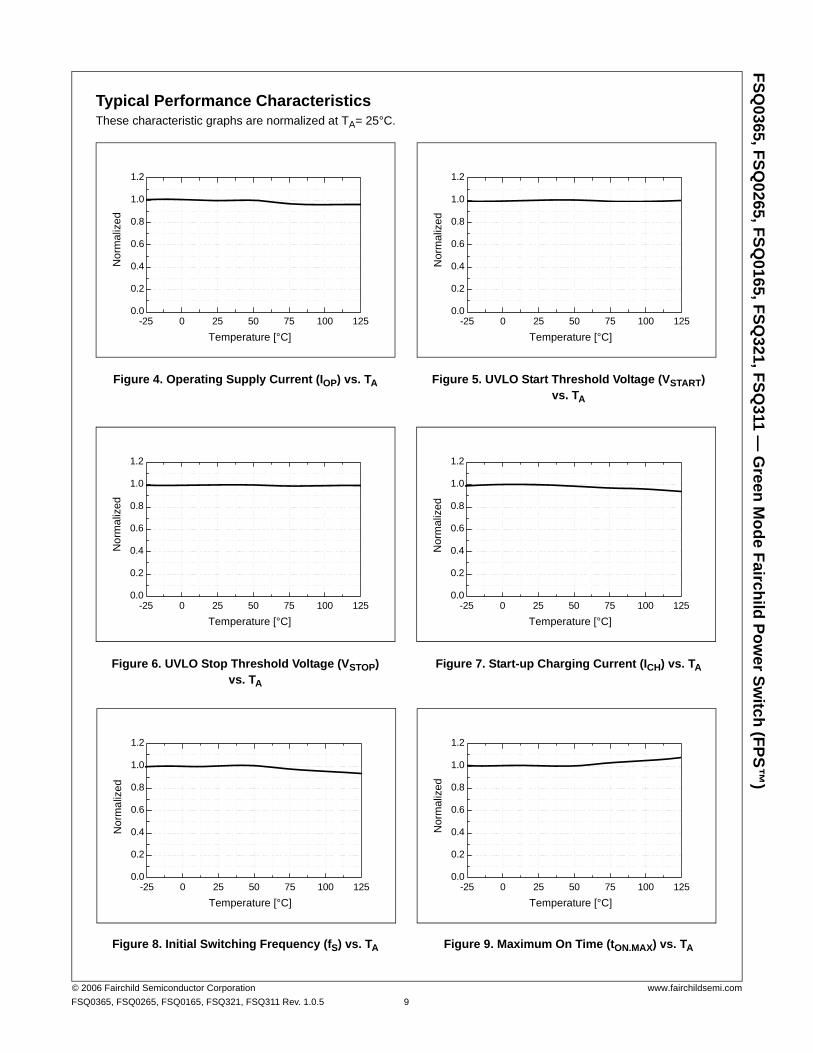
Typical Performance CharacteristicsThese characteristic graphs are normalized at TA= 25°C.
Figure 4. Operating Supply Current (IOP) vs. TA Figure 5. UVLO Start Threshold Voltage (VSTART) vs. TA
Figure 6. UVLO Stop Threshold Voltage (VSTOP) vs. TA
Figure 7. Start-up Charging Current (ICH) vs. TA
Figure 8. Initial Switching Frequency (fS) vs. TA Figure 9. Maximum On Time (tON.MAX) vs. TA
-25 0 25 50 75 100 1250.0
0.2
0.4
0.6
0.8
1.0
1.2
Nor
mal
ized
Temperature [°C]-25 0 25 50 75 100 125
0.0
0.2
0.4
0.6
0.8
1.0
1.2
Nor
mal
ized
Temperature [°C]
-25 0 25 50 75 100 1250.0
0.2
0.4
0.6
0.8
1.0
1.2
Nor
mal
ized
Temperature [°C]-25 0 25 50 75 100 125
0.0
0.2
0.4
0.6
0.8
1.0
1.2
N
orm
aliz
ed
Temperature [°C]
-25 0 25 50 75 100 1250.0
0.2
0.4
0.6
0.8
1.0
1.2
Nor
mal
ized
Temperature [°C]-25 0 25 50 75 100 125
0.0
0.2
0.4
0.6
0.8
1.0
1.2
Nor
mal
ized
Temperature [°C]
006 Fairchild Semiconductor Corporation www.fairchildsemi.com0365, FSQ0265, FSQ0165, FSQ321, FSQ311 Rev. 1.0.5 9
FSQ0365, FSQ
0265, FSQ0165, FSQ
321, FSQ311 —
Green M
ode Fairchild Power Sw
itch (FPS™)
© 2FSQ
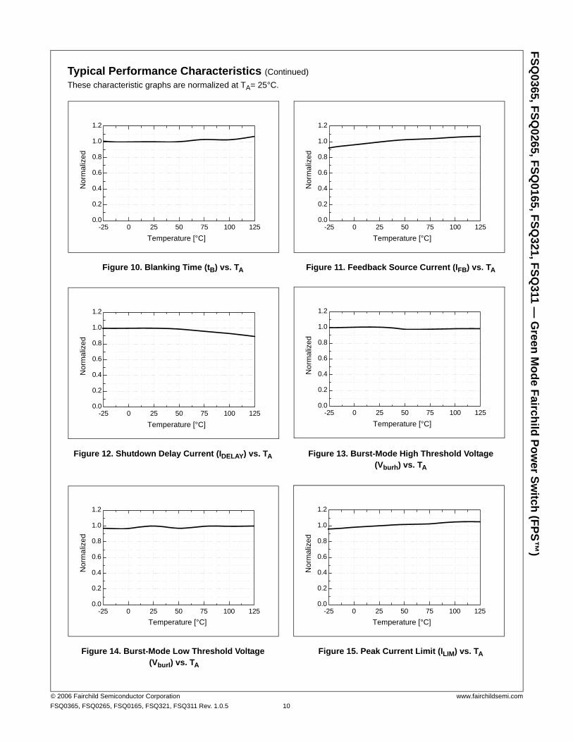
Typical Performance Characteristics (Continued)These characteristic graphs are normalized at TA= 25°C.
Figure 10. Blanking Time (tB) vs. TA Figure 11. Feedback Source Current (IFB) vs. TA
Figure 12. Shutdown Delay Current (IDELAY) vs. TA Figure 13. Burst-Mode High Threshold Voltage (Vburh) vs. TA
Figure 14. Burst-Mode Low Threshold Voltage (Vburl) vs. TA
Figure 15. Peak Current Limit (ILIM) vs. TA
-25 0 25 50 75 100 1250.0
0.2
0.4
0.6
0.8
1.0
1.2
Nor
mal
ized
Temperature [°C]-25 0 25 50 75 100 125
0.0
0.2
0.4
0.6
0.8
1.0
1.2
Nor
mal
ized
Temperature [°C]
-25 0 25 50 75 100 1250.0
0.2
0.4
0.6
0.8
1.0
1.2
Nor
mal
ized
Temperature [°C]-25 0 25 50 75 100 125
0.0
0.2
0.4
0.6
0.8
1.0
1.2
N
orm
aliz
ed
Temperature [°C]
-25 0 25 50 75 100 1250.0
0.2
0.4
0.6
0.8
1.0
1.2
Nor
mal
ized
Temperature [°C]-25 0 25 50 75 100 125
0.0
0.2
0.4
0.6
0.8
1.0
1.2
Nor
mal
ized
Temperature [°C]
006 Fairchild Semiconductor Corporation www.fairchildsemi.com0365, FSQ0265, FSQ0165, FSQ321, FSQ311 Rev. 1.0.5 10
FSQ0365, FSQ
0265, FSQ0165, FSQ
321, FSQ311 —
Green M
ode Fairchild Power Sw
itch (FPS™)
© 2FSQ
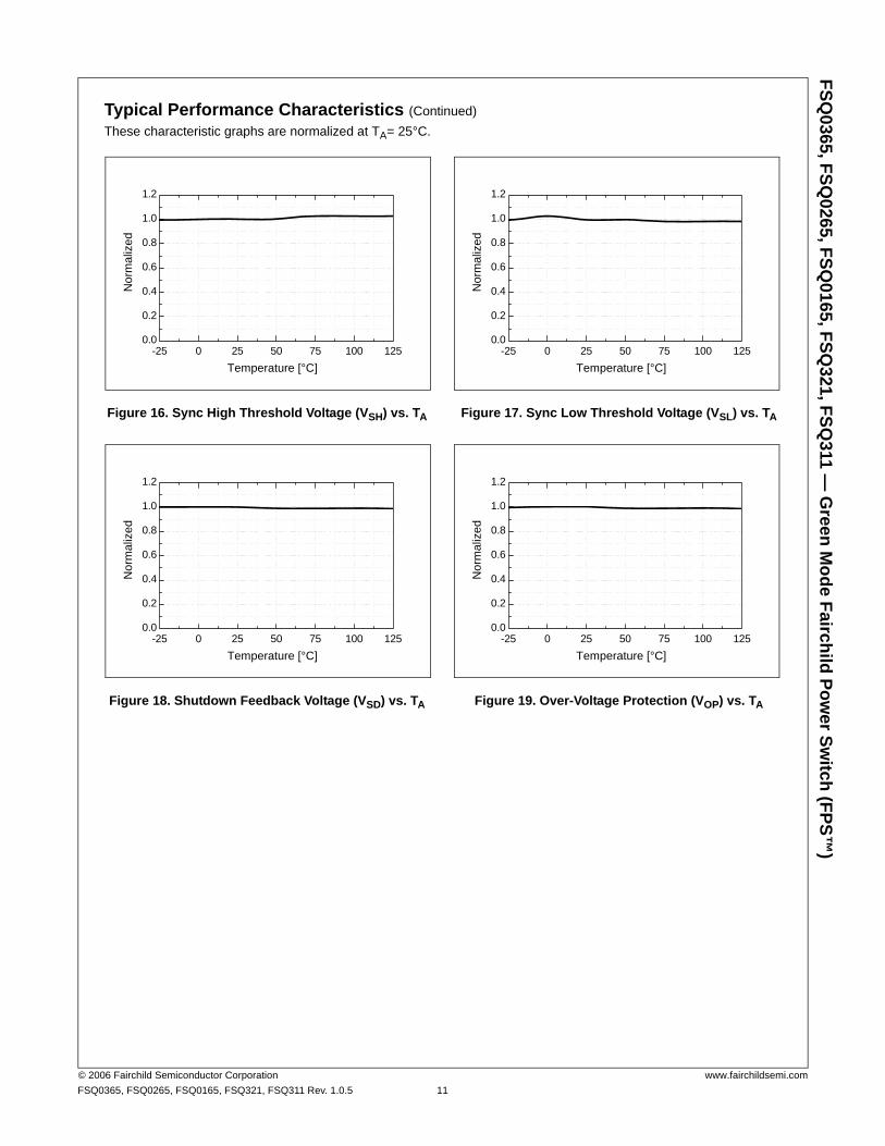
Typical Performance Characteristics (Continued)These characteristic graphs are normalized at TA= 25°C.
Figure 16. Sync High Threshold Voltage (VSH) vs. TA Figure 17. Sync Low Threshold Voltage (VSL) vs. TA
Figure 18. Shutdown Feedback Voltage (VSD) vs. TA Figure 19. Over-Voltage Protection (VOP) vs. TA
-25 0 25 50 75 100 1250.0
0.2
0.4
0.6
0.8
1.0
1.2
Nor
mal
ized
Temperature [°C]-25 0 25 50 75 100 125
0.0
0.2
0.4
0.6
0.8
1.0
1.2
Nor
mal
ized
Temperature [°C]
-25 0 25 50 75 100 1250.0
0.2
0.4
0.6
0.8
1.0
1.2
Nor
mal
ized
Temperature [°C]-25 0 25 50 75 100 125
0.0
0.2
0.4
0.6
0.8
1.0
1.2
N
orm
aliz
ed
Temperature [°C]
006 Fairchild Semiconductor Corporation www.fairchildsemi.com0365, FSQ0265, FSQ0165, FSQ321, FSQ311 Rev. 1.0.5 11
FSQ0365, FSQ
0265, FSQ0165, FSQ
321, FSQ311 —
Green M
ode Fairchild Power Sw
itch (FPS™)
© 2FSQ
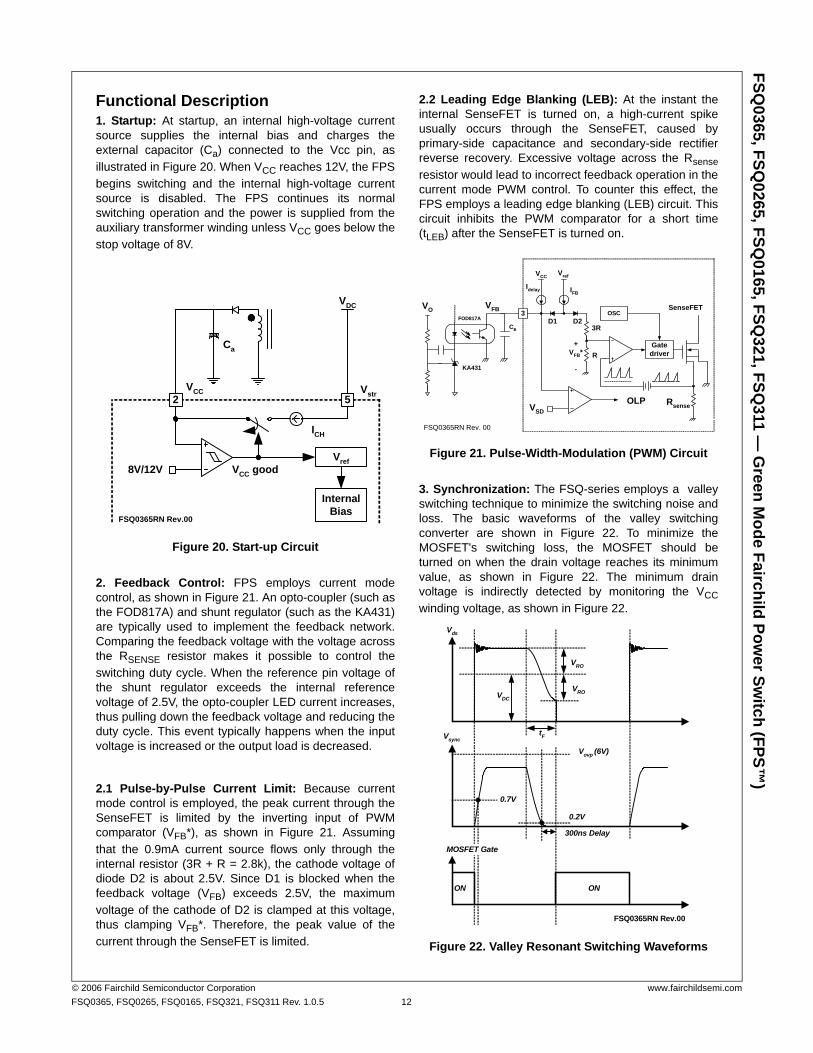
Functional Description1. Startup: At startup, an internal high-voltage currentsource supplies the internal bias and charges theexternal capacitor (Ca) connected to the Vcc pin, asillustrated in Figure 20. When VCC reaches 12V, the FPSbegins switching and the internal high-voltage currentsource is disabled. The FPS continues its normalswitching operation and the power is supplied from theauxiliary transformer winding unless VCC goes below thestop voltage of 8V.
Figure 20. Start-up Circuit
2. Feedback Control: FPS employs current modecontrol, as shown in Figure 21. An opto-coupler (such asthe FOD817A) and shunt regulator (such as the KA431)are typically used to implement the feedback network.Comparing the feedback voltage with the voltage acrossthe RSENSE resistor makes it possible to control theswitching duty cycle. When the reference pin voltage ofthe shunt regulator exceeds the internal referencevoltage of 2.5V, the opto-coupler LED current increases,thus pulling down the feedback voltage and reducing theduty cycle. This event typically happens when the inputvoltage is increased or the output load is decreased.
2.1 Pulse-by-Pulse Current Limit: Because currentmode control is employed, the peak current through theSenseFET is limited by the inverting input of PWMcomparator (VFB*), as shown in Figure 21. Assumingthat the 0.9mA current source flows only through theinternal resistor (3R + R = 2.8k), the cathode voltage ofdiode D2 is about 2.5V. Since D1 is blocked when thefeedback voltage (VFB) exceeds 2.5V, the maximumvoltage of the cathode of D2 is clamped at this voltage,thus clamping VFB*. Therefore, the peak value of thecurrent through the SenseFET is limited.
2.2 Leading Edge Blanking (LEB): At the instant theinternal SenseFET is turned on, a high-current spikeusually occurs through the SenseFET, caused byprimary-side capacitance and secondary-side rectifierreverse recovery. Excessive voltage across the Rsenseresistor would lead to incorrect feedback operation in thecurrent mode PWM control. To counter this effect, theFPS employs a leading edge blanking (LEB) circuit. Thiscircuit inhibits the PWM comparator for a short time(tLEB) after the SenseFET is turned on.
Figure 21. Pulse-Width-Modulation (PWM) Circuit
3. Synchronization: The FSQ-series employs a valleyswitching technique to minimize the switching noise andloss. The basic waveforms of the valley switchingconverter are shown in Figure 22. To minimize theMOSFET's switching loss, the MOSFET should beturned on when the drain voltage reaches its minimumvalue, as shown in Figure 22. The minimum drainvoltage is indirectly detected by monitoring the VCCwinding voltage, as shown in Figure 22.
Figure 22. Valley Resonant Switching Waveforms
8V/12VVref
InternalBias
VCC Vstr
ICH
VCC good
VDC
Ca
FSQ0365RN Rev.00
2 5
3 OSC
VCC Vref
Idelay IFB
VSD
R
3R
Gatedriver
OLP
D1 D2
+VFB*
-
VFB
KA431
CB
VOFOD817A
Rsense
SenseFET
FSQ0365RN Rev. 00
VDC
VRO
VRO
Vds
tF
0.7V
Vsync
300ns Delay
0.2V
ONON
Vovp (6V)
FSQ0365RN Rev.00
MOSFET Gate
006 Fairchild Semiconductor Corporation www.fairchildsemi.com0365, FSQ0265, FSQ0165, FSQ321, FSQ311 Rev. 1.0.5 12
FSQ0365, FSQ
0265, FSQ0165, FSQ
321, FSQ311 —
Green M
ode Fairchild Power Sw
itch (FPS™)
© 2FSQ
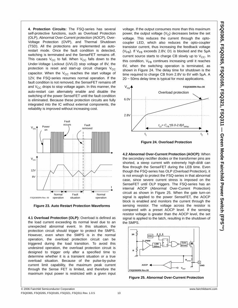
4. Protection Circuits: The FSQ-series has severalself-protective functions, such as Overload Protection(OLP), Abnormal Over-Current protection (AOCP), Over-Voltage Protection (OVP), and Thermal Shutdown(TSD). All the protections are implemented as auto-restart mode. Once the fault condition is detected,switching is terminated and the SenseFET remains off.This causes VCC to fall. When VCC falls down to theUnder-Voltage Lockout (UVLO) stop voltage of 8V, theprotection is reset and start-up circuit charges VCCcapacitor. When the VCC reaches the start voltage of12V, the FSQ-series resumes normal operation. If thefault condition is not removed, the SenseFET remains offand VCC drops to stop voltage again. In this manner, theauto-restart can alternately enable and disable theswitching of the power SenseFET until the fault conditionis eliminated. Because these protection circuits are fullyintegrated into the IC without external components, thereliability is improved without increasing cost.
Figure 23. Auto Restart Protection Waveforms
4.1 Overload Protection (OLP): Overload is defined asthe load current exceeding its normal level due to anunexpected abnormal event. In this situation, theprotection circuit should trigger to protect the SMPS.However, even when the SMPS is in the normaloperation, the overload protection circuit can betriggered during the load transition. To avoid thisundesired operation, the overload protection circuit isdesigned to trigger only after a specified time todetermine whether it is a transient situation or a trueoverload situation. Because of the pulse-by-pulsecurrent limit capability, the maximum peak currentthrough the Sense FET is limited, and therefore themaximum input power is restricted with a given input
voltage. If the output consumes more than this maximumpower, the output voltage (VO) decreases below the setvoltage. This reduces the current through the opto-coupler LED, which also reduces the opto-couplertransistor current, thus increasing the feedback voltage(VFB). If VFB exceeds 2.8V, D1 is blocked and the 5µAcurrent source starts to charge CB slowly up to VCC. Inthis condition, VFB continues increasing until it reaches6V, when the switching operation is terminated, asshown in Figure 24. The delay time for shutdown is thetime required to charge CB from 2.8V to 6V with 5µA. A20 ~ 50ms delay time is typical for most applications.
Figure 24. Overload Protection
4.2 Abnormal Over-Current Protection (AOCP): Whenthe secondary rectifier diodes or the transformer pins areshorted, a steep current with extremely high-di/dt canflow through the SenseFET during the LEB time. Eventhough the FSQ-series has OLP (Overload Protection), itis not enough to protect the FSQ-series in that abnormalcase, since severe current stress is imposed on theSenseFET until OLP triggers. The FSQ-series has aninternal AOCP (Abnormal Over-Current Protection)circuit as shown in Figure 25. When the gate turn-onsignal is applied to the power SenseFET, the AOCPblock is enabled and monitors the current through thesensing resistor. The voltage across the resistor iscompared with a preset AOCP level. If the sensingresistor voltage is greater than the AOCP level, the setsignal is applied to the latch, resulting in the shutdown ofthe SMPS.
Figure 25. Abnormal Over-Current Protection
Faultsituation
8V
12V
VCC
VDS
t
Faultoccurs Fault
removed
Normaloperation
Normaloperation
Poweron
FSQ0365RN Rev. 00
VFB
t
2.8V
6.0V
Overload protection
t12= CFB*(6.0-2.8)/Idelay
t1 t2
FSQ0365RN Rev.00
1
S
Q
Q
R
OSC
R
3R
GND
GatedriverLEB
200ns
PWM
+
- VOCP
AOCP
Rsense
FSQ0365RN Rev.00
006 Fairchild Semiconductor Corporation www.fairchildsemi.com0365, FSQ0265, FSQ0165, FSQ321, FSQ311 Rev. 1.0.5 13
FSQ0365, FSQ
0265, FSQ0165, FSQ
321, FSQ311 —
Green M
ode Fairchild Power Sw
itch (FPS™)
© 2FSQ
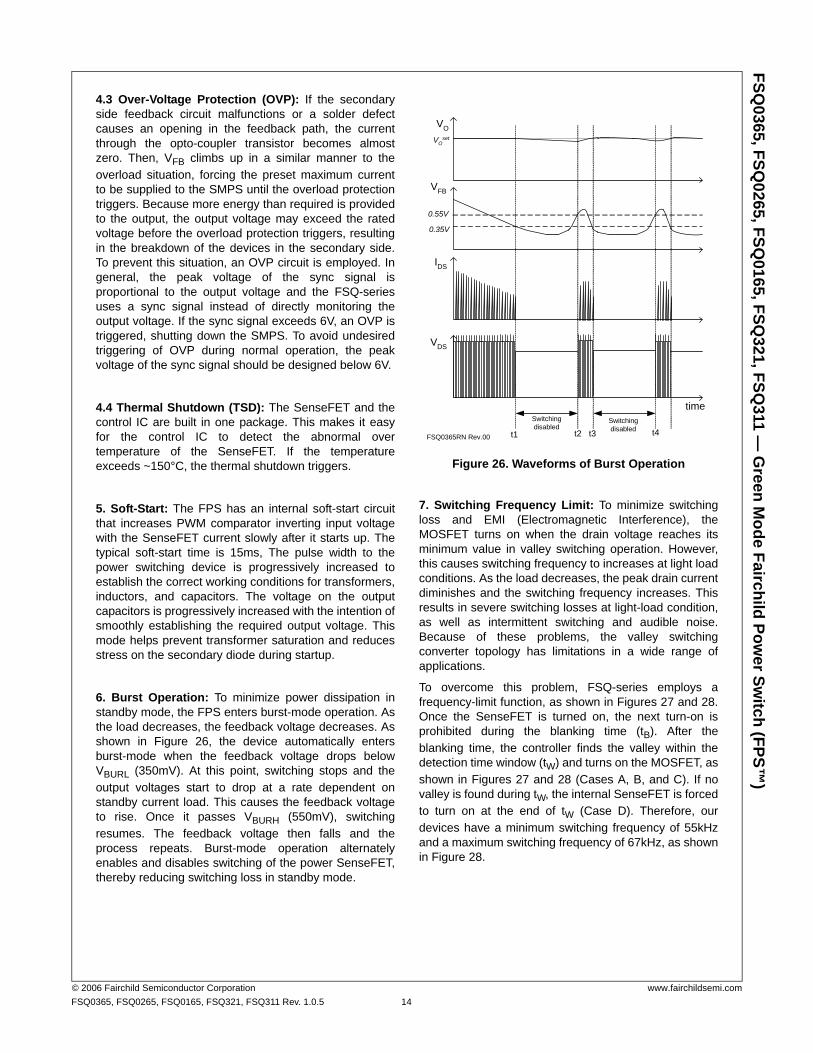
4.3 Over-Voltage Protection (OVP): If the secondaryside feedback circuit malfunctions or a solder defectcauses an opening in the feedback path, the currentthrough the opto-coupler transistor becomes almostzero. Then, VFB climbs up in a similar manner to theoverload situation, forcing the preset maximum currentto be supplied to the SMPS until the overload protectiontriggers. Because more energy than required is providedto the output, the output voltage may exceed the ratedvoltage before the overload protection triggers, resultingin the breakdown of the devices in the secondary side.To prevent this situation, an OVP circuit is employed. Ingeneral, the peak voltage of the sync signal isproportional to the output voltage and the FSQ-seriesuses a sync signal instead of directly monitoring theoutput voltage. If the sync signal exceeds 6V, an OVP istriggered, shutting down the SMPS. To avoid undesiredtriggering of OVP during normal operation, the peakvoltage of the sync signal should be designed below 6V.
4.4 Thermal Shutdown (TSD): The SenseFET and thecontrol IC are built in one package. This makes it easyfor the control IC to detect the abnormal overtemperature of the SenseFET. If the temperatureexceeds ~150°C, the thermal shutdown triggers.
5. Soft-Start: The FPS has an internal soft-start circuitthat increases PWM comparator inverting input voltagewith the SenseFET current slowly after it starts up. Thetypical soft-start time is 15ms, The pulse width to thepower switching device is progressively increased toestablish the correct working conditions for transformers,inductors, and capacitors. The voltage on the outputcapacitors is progressively increased with the intention ofsmoothly establishing the required output voltage. Thismode helps prevent transformer saturation and reducesstress on the secondary diode during startup.
6. Burst Operation: To minimize power dissipation instandby mode, the FPS enters burst-mode operation. Asthe load decreases, the feedback voltage decreases. Asshown in Figure 26, the device automatically entersburst-mode when the feedback voltage drops belowVBURL (350mV). At this point, switching stops and theoutput voltages start to drop at a rate dependent onstandby current load. This causes the feedback voltageto rise. Once it passes VBURH (550mV), switchingresumes. The feedback voltage then falls and theprocess repeats. Burst-mode operation alternatelyenables and disables switching of the power SenseFET,thereby reducing switching loss in standby mode.
Figure 26. Waveforms of Burst Operation
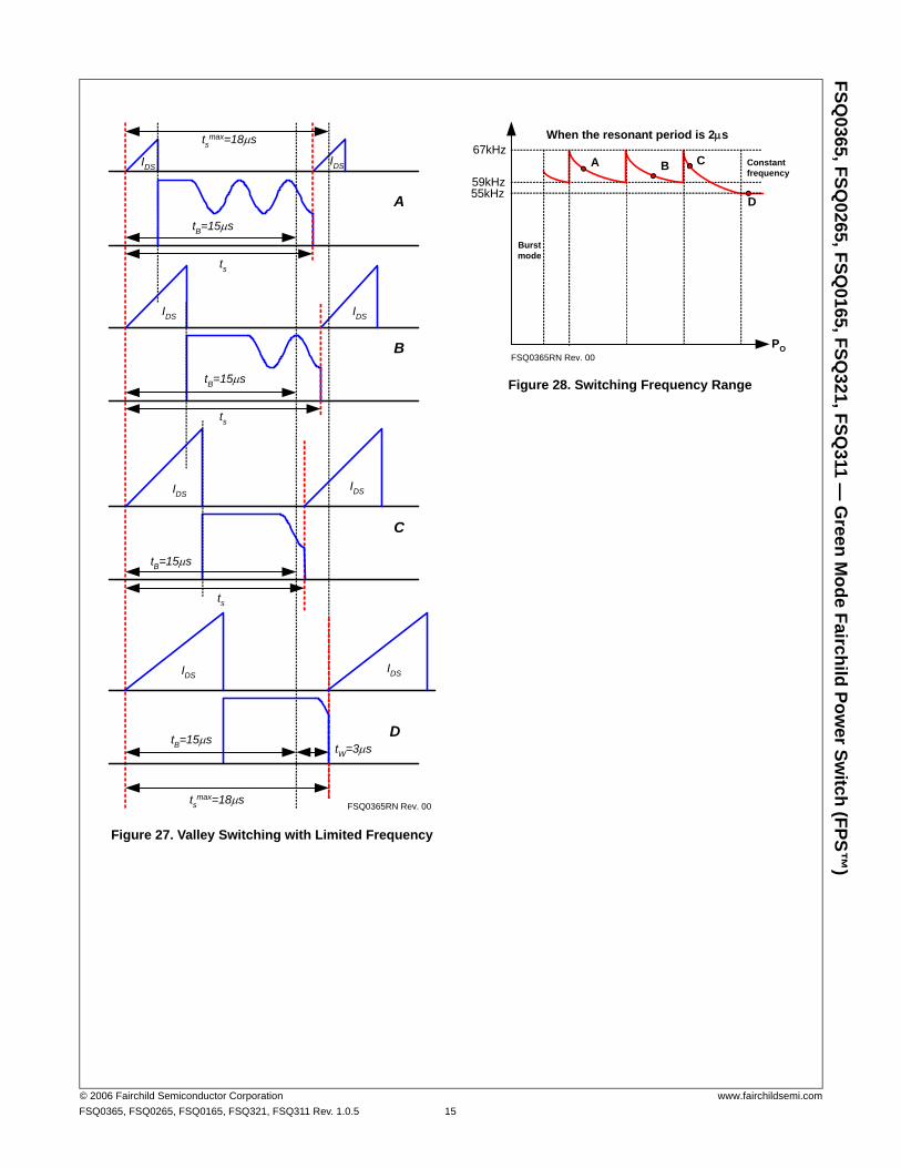
7. Switching Frequency Limit: To minimize switchingloss and EMI (Electromagnetic Interference), theMOSFET turns on when the drain voltage reaches itsminimum value in valley switching operation. However,this causes switching frequency to increases at light loadconditions. As the load decreases, the peak drain currentdiminishes and the switching frequency increases. Thisresults in severe switching losses at light-load condition,as well as intermittent switching and audible noise.Because of these problems, the valley switchingconverter topology has limitations in a wide range ofapplications.
To overcome this problem, FSQ-series employs afrequency-limit function, as shown in Figures 27 and 28.Once the SenseFET is turned on, the next turn-on isprohibited during the blanking time (tB). After theblanking time, the controller finds the valley within thedetection time window (tW) and turns on the MOSFET, asshown in Figures 27 and 28 (Cases A, B, and C). If novalley is found during tW, the internal SenseFET is forcedto turn on at the end of tW (Case D). Therefore, ourdevices have a minimum switching frequency of 55kHzand a maximum switching frequency of 67kHz, as shownin Figure 28.
VFB
VDS
0.35V
0.55V
IDS
VO
VOset
timeSwitchingdisabled
t1 t2 t3Switchingdisabled t4FSQ0365RN Rev.00
006 Fairchild Semiconductor Corporation www.fairchildsemi.com0365, FSQ0265, FSQ0165, FSQ321, FSQ311 Rev. 1.0.5 14
FSQ0365, FSQ
0265, FSQ0165, FSQ
321, FSQ311 —
Green M
ode Fairchild Power Sw
itch (FPS™)
© 2FSQ
Figure 27. Valley Switching with Limited Frequency
Figure 28. Switching Frequency Range
tsmax=18μs
tsmax=18μs
tB=15μs
ts
tB=15μs
ts
ts
IDSIDS
IDSIDS
A
B
C
DtW=3μs
tB=15μs
tB=15μs
IDSIDS
IDSIDS
FSQ0365RN Rev. 00
55kHz
67kHz
59kHz
Burstmode
Constantfrequency
D
CBA
PO
When the resonant period is 2μs
FSQ0365RN Rev. 00
006 Fairchild Semiconductor Corporation www.fairchildsemi.com0365, FSQ0265, FSQ0165, FSQ321, FSQ311 Rev. 1.0.5 15
FSQ0365, FSQ
0265, FSQ0165, FSQ
321, FSQ311 —
Green M
ode Fairchild Power Sw
itch (FPS™)
© 2FSQ
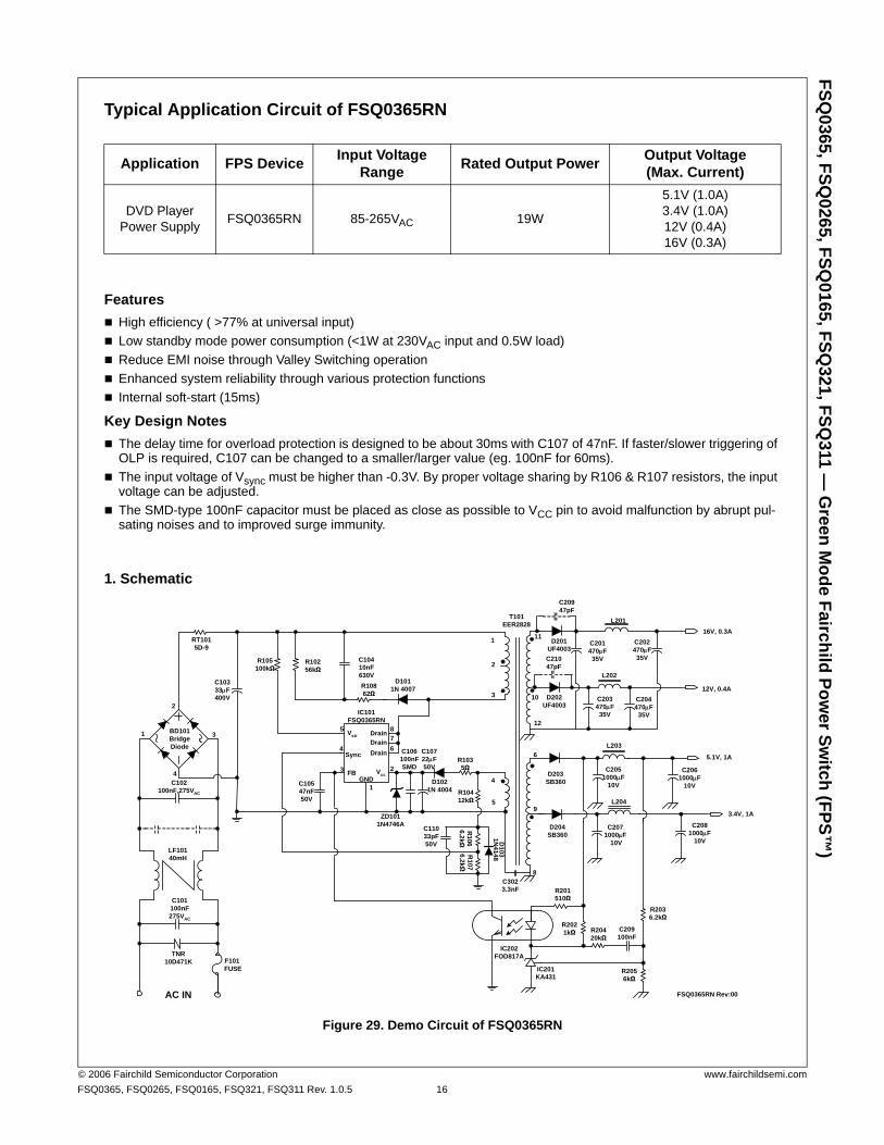
Typical Application Circuit of FSQ0365RN
FeaturesHigh efficiency ( >77% at universal input)Low standby mode power consumption (<1W at 230VAC input and 0.5W load)Reduce EMI noise through Valley Switching operationEnhanced system reliability through various protection functionsInternal soft-start (15ms)
Key Design NotesThe delay time for overload protection is designed to be about 30ms with C107 of 47nF. If faster/slower triggering of OLP is required, C107 can be changed to a smaller/larger value (eg. 100nF for 60ms).The input voltage of Vsync must be higher than -0.3V. By proper voltage sharing by R106 & R107 resistors, the input voltage can be adjusted.The SMD-type 100nF capacitor must be placed as close as possible to VCC pin to avoid malfunction by abrupt pul-sating noises and to improved surge immunity.
1. Schematic
Figure 29. Demo Circuit of FSQ0365RN
Application FPS Device Input Voltage Range Rated Output Power Output Voltage
(Max. Current)
DVD Player Power Supply FSQ0365RN 85-265VAC 19W
5.1V (1.0A)3.4V (1.0A)12V (0.4A)16V (0.3A)
3
4C102
100nF,275VAC
LF10140mH
C101100nF275VAC
F101 FUSE
C10333μF400V
R10256kΩ
C10410nF630V
D1011N 4007
IC101FSQ0365RN
C10547nF50V
C10722μF50V
D1021N 4004
R1035Ω
1
2
3
4
5
8
9
6
12
10
11
T101EER2828
D201UF4003
C201470μF35V
C202470μF35V
L201
L203
L204
D202UF4003
C203470μF35V
C204470μF
35V
C2061000μF
10V
C2051000μF
10VD203
SB360
D204SB360
C2071000μF
10V
C2081000μF
10V
R201510Ω
R2021kΩ
R2036.2kΩ
R20420kΩ
C209100nF
R2056kΩ
IC202FOD817A
BD101BridgeDiode
L202
Vstr
Sync
FB Vcc
Drain
GND
6
1
23
4
51
2
DrainDrain
78
IC201KA431
16V, 0.3A
12V, 0.4A
5.1V, 1A
3.4V, 1A
R10412kΩ
TNR10D471K
R105100kΩ
R106
6.2kΩ
C3023.3nF
AC IN
C106100nFSMD
D103
1N4148
C11033pF50V
ZD1011N4746A
R107
6.2kΩ
RT1015D-9
R10862Ω
C20947pF
C21047pF
FSQ0365RN Rev:00
006 Fairchild Semiconductor Corporation www.fairchildsemi.com0365, FSQ0265, FSQ0165, FSQ321, FSQ311 Rev. 1.0.5 16
FSQ0365, FSQ
0265, FSQ0165, FSQ
321, FSQ311 —
Green M
ode Fairchild Power Sw
itch (FPS™)
© 2FSQ
2. Transformer
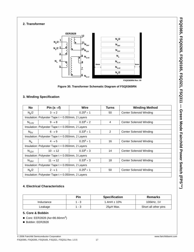
Figure 30. Transformer Schematic Diagram of FSQ0365RN
3. Winding Specification
4. Electrical Characteristics
5. Core & BobbinCore: EER2828 (Ae=86.66mm2)Bobbin: EER2828
No Pin (s→f) Wire Turns Winding MethodNp/2 3 → 2 0.25φ × 1 50 Center Solenoid Winding
Insulation: Polyester Tape t = 0.050mm, 2 Layers
N3.4V 9 → 8 0.33φ × 2 4 Center Solenoid Winding
Insulation: Polyester Tape t = 0.050mm, 2 Layers
N5V 6 → 9 0.33φ × 1 2 Center Solenoid Winding
Insulation: Polyester Tape t = 0.050mm, 2 Layers
Na 4 → 5 0.25φ × 1 16 Center Solenoid Winding
Insulation: Polyester Tape t = 0.050mm, 2 Layers
N12V 10 → 12 0.33φ × 3 14 Center Solenoid Winding
Insulation: Polyester Tape t = 0.050mm, 3 Layers
N16V 11 → 12 0.33φ × 3 18 Center Solenoid Winding
Insulation: Polyester Tape t = 0.050mm, 2 Layers
Np/2 2 → 1 0.25φ × 1 50 Center Solenoid Winding
Insulation: Polyester Tape t = 0.050mm, 2 Layers
Pin Specification RemarksInductance 1 - 3 1.4mH ± 10% 100kHz, 1V
Leakage 1 - 3 25µH Max. Short all other pins
EER2828
N12V
1
6
7
8
9
10
11
12
N16V
N5.1V
N3.4V
Np/2
Na
2
3
4
5
Np/2N16V
N12V
Na
N5.1V
N3.4V
Np/2
Np/2
6mm 3mm
FSQ0365RN Rev: 00
006 Fairchild Semiconductor Corporation www.fairchildsemi.com0365, FSQ0265, FSQ0165, FSQ321, FSQ311 Rev. 1.0.5 17
FSQ0365, FSQ
0265, FSQ0165, FSQ
321, FSQ311 —
Green M
ode Fairchild Power Sw
itch (FPS™)
© 2FSQ
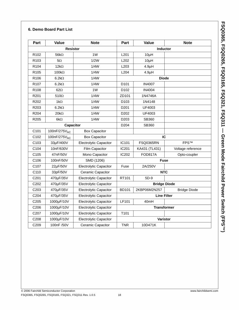
6. Demo Board Part List
Part Value Note Part Value NoteResistor Inductor
R102 56kΩ 1W L201 10µH
R103 5Ω 1/2W L202 10µH
R104 12kΩ 1/4W L203 4.9µH
R105 100kΩ 1/4W L204 4.9µH
R106 6.2kΩ 1/4W DiodeR107 6.2kΩ 1/4W D101 IN4007
R108 62Ω 1W D102 IN4004
R201 510Ω 1/4W ZD101 1N4746A
R202 1kΩ 1/4W D103 1N4148
R203 6.2kΩ 1/4W D201 UF4003
R204 20kΩ 1/4W D202 UF4003
R205 6kΩ 1/4W D203 SB360
Capacitor D204 SB360
C101 100nF/275VAC Box Capacitor
C102 100nF/275VAC Box Capacitor ICC103 33µF/400V Electrolytic Capacitor IC101 FSQ0365RN FPS™
C104 10nF/630V Film Capacitor IC201 KA431 (TL431) Voltage reference
C105 47nF/50V Mono Capacitor IC202 FOD817A Opto-coupler
C106 100nF/50V SMD (1206) FuseC107 22µF/50V Electrolytic Capacitor Fuse 2A/250V
C110 33pF/50V Ceramic Capacitor NTCC201 470µF/35V Electrolytic Capacitor RT101 5D-9
C202 470µF/35V Electrolytic Capacitor Bridge DiodeC203 470µF/35V Electrolytic Capacitor BD101 2KBP06M2N257 Bridge Diode
C204 470µF/35V Electrolytic Capacitor Line FilterC205 1000µF/10V Electrolytic Capacitor LF101 40mH
C206 1000µF/10V Electrolytic Capacitor TransformerC207 1000µF/10V Electrolytic Capacitor T101
C208 1000µF/10V Electrolytic Capacitor VaristorC209 100nF /50V Ceramic Capacitor TNR 10D471K
006 Fairchild Semiconductor Corporation www.fairchildsemi.com0365, FSQ0265, FSQ0165, FSQ321, FSQ311 Rev. 1.0.5 18
FSQ0365, FSQ
0265, FSQ0165, FSQ
321, FSQ311 —
Green M
ode Fairchild Power Sw
itch (FPS™)
© 2FSQ
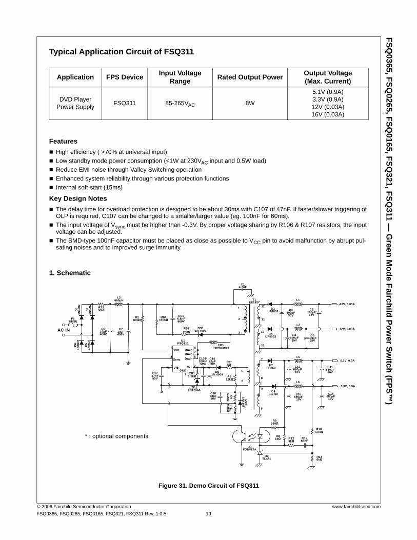
Typical Application Circuit of FSQ311
FeaturesHigh efficiency ( >70% at universal input)Low standby mode power consumption (<1W at 230VAC input and 0.5W load)Reduce EMI noise through Valley Switching operationEnhanced system reliability through various protection functionsInternal soft-start (15ms)
Key Design NotesThe delay time for overload protection is designed to be about 30ms with C107 of 47nF. If faster/slower triggering of OLP is required, C107 can be changed to a smaller/larger value (eg. 100nF for 60ms).The input voltage of Vsync must be higher than -0.3V. By proper voltage sharing by R106 & R107 resistors, the input voltage can be adjusted.The SMD-type 100nF capacitor must be placed as close as possible to VCC pin to avoid malfunction by abrupt pul-sating noises and to improved surge immunity.
1. Schematic
Figure 31. Demo Circuit of FSQ311
Application FPS Device Input Voltage Range Rated Output Power Output Voltage
(Max. Current)
DVD Player Power Supply FSQ311 85-265VAC 8W
5.1V (0.9A)3.3V (0.9A)12V (0.03A)16V (0.03A)
F1 FUSE
C610μF400V
RS5150kΩ
CS5 6.8nF680V
DS1 1N 4007
U1FSQ311
C1747nF50V
C1422μF50V
D81N 4004
R4*5Ω
1
2
3
5
6
8
9
7
11
10
12
T1EE1927
D1UF4003 C3
100μF35V
C2100μF35V
L1
L5
L6
D4UF4003 C4
100μF35V
C5100μF
35V
C11680μF10V
C12680μF10V
D7SB360
D9SB360 C15
680μF 10V
C16680μF
10V
R6510Ω
R81kΩ
R106.2kΩ
R128kΩ
C1968nF
R136kΩ
U3FOD817A
L3
Vstr
Sync
Vfb Vcc
Drain
GND
6
1
23
4
5
DrainDrain
78
U2TL431
-12V, 0.03A
12V, 0.03A
5.1V, 0.9A
3.3V, 0.9A
R512kΩ
R2100kΩ
R7
6.2kΩ
C14.7nF
AC IN
C104*100nFSMD
D10
1N4148
C1833pF50V
ZD11N4746A
R11
6.2kΩ
RT15D-9
RS6200Ω
C710μF400V
D3
1N40
07
D2
1N40
07
D6
1N40
07
D5
1N40
07
L2660μH
ZR11.2kΩ
* : optional components
8
11
FB1 Ferritebead
006 Fairchild Semiconductor Corporation www.fairchildsemi.com0365, FSQ0265, FSQ0165, FSQ321, FSQ311 Rev. 1.0.5 19
FSQ0365, FSQ
0265, FSQ0165, FSQ
321, FSQ311 —
Green M
ode Fairchild Power Sw
itch (FPS™)
© 2FSQ
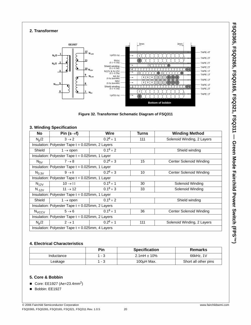
2. Transformer
Figure 32. Transformer Schematic Diagram of FSQ311
3. Winding Specification
4. Electrical Characteristics
5. Core & Bobbin Core: EE1927 (Ae=23.4mm2) Bobbin: EE1927
No Pin (s→f) Wire Turns Winding MethodNp/2 3 → 2 0.2φ × 1 111 Solenoid Winding, 2 Layers
Insulation: Polyester Tape t = 0.025mm, 2 LayersShield 1 → open 0.1φ × 2 Shield winding
Insulation: Polyester Tape t = 0.025mm, 1 LayerN5V 7 → 8 0.2φ × 3 15 Center Solenoid Winding
Insulation: Polyester Tape t = 0.025mm, 1 LayerN3.3V 9 → 8 0.2φ × 3 10 Center Solenoid Winding
Insulation: Polyester Tape t = 0.025mm, 1 LayerN12V 10 → 11 0.1φ × 1 30 Solenoid WindingN-12V 11 → 12 0.1φ × 3 33 Solenoid Winding
Insulation: Polyester Tape t = 0.025mm, 1 Layer Shield 1 → open 0.1φ × 2 Shield winding
Insulation: Polyester Tape t = 0.025mm, 2 Layers NVCCV 5 → 6 0.1φ × 1 36 Center Solenoid Winding
Insulation: Polyester Tape t = 0.025mm, 2 LayersNp/2 2 → 1 0.2φ × 1 111 Solenoid Winding, 2 Layers
Insulation: Polyester Tape t = 0.025mm, 4 Layers
Pin Specification RemarksInductance 1 - 3 2.1mH ± 10% 66kHz, 1VLeakage 1 - 3 100µH Max. Short all other pins
EE1927
1Np/2
NVCC
2
3
5
6
Np/2
N5V
N3.3V
N12V
N-12V12
11
10
9
8
7
3
2
11 1012 11
6 5
2
1
Bottom of bobbin
3mm 3mm
Shield winding(0.1~0.15φ)
Lp/2(0.2φ)
N5V(0.2φ,3parallel)
N3.3V(0.2φ,3parallel)
N12V & N-12V(0.1~0.15φ)
NVcc(0.1~0.15φ)
Lp/2(0.2φ)
TAPE 1T
TAPE 2T
TAPE 1T
TAPE 1TTAPE 1TTAPE 2T
TAPE 2T
TAPE 4T
8 8 8 7 7 7
8 8 8 9 9 9
11
11
TAPE 2TShield winding
(0.1~0.15φ)
TAPE 1T
006 Fairchild Semiconductor Corporation www.fairchildsemi.com0365, FSQ0265, FSQ0165, FSQ321, FSQ311 Rev. 1.0.5 20
FSQ0365, FSQ
0265, FSQ0165, FSQ
321, FSQ311 —
Green M
ode Fairchild Power Sw
itch (FPS™)
© 2FSQ
6. Demo Board Part List
Part Value Note Part Value NoteResistor Inductor
R2 100kΩ 1/4W L2 660µH
ZR1 1.2kΩ 1/4W L1 4.7µH
R4 5Ω 1/2W L3 4.7µH
R5 12kΩ 1/4W L5 4.7µH
R7 6.2kΩ 1/4W L6 4.7µH
R11 6.2kΩ 1/4W DiodeRS5 150kΩ 2W D2,3,4,5 IN4007
RS6 200Ω 1W D8 IN4004
R6 510Ω 1/4W D10 1N4148
R8 1kΩ 1/4W ZD1 1N4746A
R12 8kΩ 1/4W DS1 1N4007
R10 6.2kΩ 1/4W, 1% D1 UF4003
R13 6kΩ 1/4W, 1% D4 UF4003
Capacitor D7 SB360
C6 10µF/400V Electrolytic D9 SB360
C7 10µF/400V Electrolytic ICC17 47nF/50V Ceramic U1 FSQ311 FPS™
C104 100nF/50V SMD(1206) U2 KA431 (TL431) Voltage reference
C14 22µF/50V Electrolytic U3 FOD817A Opto-coupler
C18 33pF/50V Ceramic FuseCS5 6.8nF/680V Film Fuse 2A/250V
C2 100µF/35V Electrolytic NTCC3 100µF/35V Electrolytic RT1 5D-9
C4 100µF/35V Electrolytic TransformerC5 100µF/35V Electrolytic T1 EE1927 Bridge Diode
C11 680µF/10V Electrolytic Ferrite beadC12 680µF/10V Electrolytic FB1
C15 680µF/10V Electrolytic
C16 680µF/10V Electrolytic
C19 68nµF/50V Ceramic
C1 4.7nF/375VAC Ceramic
006 Fairchild Semiconductor Corporation www.fairchildsemi.com0365, FSQ0265, FSQ0165, FSQ321, FSQ311 Rev. 1.0.5 21
FSQ0365, FSQ
0265, FSQ0165, FSQ
321, FSQ311 —
Green M
ode Fairchild Power Sw
itch (FPS™)
© 2FSQ
Package Dimensions
Figure 33. 8-Lead, Dual In-Line Package(DIP)
5.08 MAX
0.33 MIN
2.54
7.62
0.560.355
1.651.27
3.6833.20
3.603.00
6.676.096
9.839.00
7.62
9.9577.87
0.3560.20
NOTES: UNLESS OTHERWISE SPECIFIED
A) THIS PACKAGE CONFORMS TO
JEDEC MS-001 VARIATION BA
B) ALL DIMENSIONS ARE IN MILLIMETERS.
C) DIMENSIONS ARE EXCLUSIVE OF BURRS,
MOLD FLASH, AND TIE BAR EXTRUSIONS.
D) DIMENSIONS AND TOLERANCES PER
ASME Y14.5M-1994
8.2557.61
E) DRAWING FILENAME AND REVSION: MKT-N08FREV2.
(0.56)
006 Fairchild Semiconductor Corporation www.fairchildsemi.com0365, FSQ0265, FSQ0165, FSQ321, FSQ311 Rev. 1.0.5 22
FSQ0365, FSQ
0265, FSQ0165, FSQ
321, FSQ311 —
Green M
ode Fairchild Power Sw
itch (FPS™)
© 2FSQ
Package Dimensions (Continued)
Figure 34. 8-Lead, LSOP Package
MKT-MLSOP08ArevA
006 Fairchild Semiconductor Corporation www.fairchildsemi.com0365, FSQ0265, FSQ0165, FSQ321, FSQ311 Rev. 1.0.5 23
FSQ0365, FSQ
0265, FSQ0165, FSQ
321, FSQ311 —
Green M
ode Fairchild Power Sw
itch (FPS™)
© 2006 Fairchild Semiconductor Corporation www.fairchildsemi.comFSQ0365, FSQ0265, FSQ0165, FSQ321, FSQ311 Rev. 1.0.5 24