Embed Size (px)
Citation preview
May, 1977 B-77-200-2021-2
\NABCC ~
An American-Standard Company
SERVICE MANUAL 4588-A
FSO·l INVERTER FOLLOWER
INPUT STAGE
( UN451033·1601)
83.3 Hz. (UN451033·1602)
100Hz.
UNION SWITCH & SIGNAL DIVISION WESTINGHOUSE AIR BRAKE COMPANY
Swissvale, PA 15218
TABLE OF CONTENTS
Section
I GENERAL
II GENERAL EQUIPMENT DESCRIPTION
2.1 SPECIFICATIONS
III THEORY
3.1 GENERAL THEORY 3.2 DETAILED THEORY
IV INSTALLATION
V MAINTENANCE
5.1 ·FIELD MAINTENANCE 5.2 SHOP MAINTENANCE 5.3 TEST PROCEDURE
VI PARTS LIST
LIST OF ILLUSTRATIONS
Figure
1 Test Set-UP for the F50-l 2 Schematic Diagram of the F50-l Inverter
Follower (Input) 3 Inverter Follower Wiring Diagram 4 Unit Assembly, Parts Location, and Parts
List 5 Component Board, Parts Location, and Parts
List 6 Heatsink, Parts Location, and Parts List
4588-A, p. 2
Page
3
3
3
5
5 5
5
6
7 7 8
12
,::-1\
Page
9
15/16 17/18
19/20
21/22 21/22
' -I
SECTION I
GENERAL
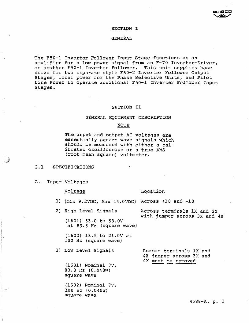
The FS0-1 Inverter Follower Input Stage functions as an amplifier for a low power signal from an F-70 Inverter-Driver, or another FS0-1 Inverter Follower. This unit supplies base drive for two separate style FS0-2 Inverter Follower Output Stages, local power for the Phase Selective Units, and Pilot Line Power to operate additional FS0-1 Inverter Follower Input Stages.
SECTION II
GENERAL EQUIPMENT DESCRIPTION
NOTE
The input and output AC voltages are essentially square wave signals which should be measured with either a calibrated oscilloscope or a true RMS (root mean square) voltmeter.
2.1 SPECIFICATIONS
A. Input
1)
2)
3)
Voltages
Voltasie
(min 9.2VDC, Max 14. OVDC)
High Level Signals
(1601) 33.0 to 58. OV at 83.3 Hz {square wave)
(1602) 13.5 to 21. ov 100 Hz {square wave)
Low Level Signals
(1601) Nominal 7V, 83.3 Hz (0.040W) square wave
{1602) Nominal 7V, 100 Hz (0.040W} square wave
at
Location
Across +10 and -10
Across terminals lX and 2X with jumper across 3X and 4X
Across terminals lX and 4X jumper across 3X and 4X must be removed.
4588-A, p. 3
WABCO ............... ~
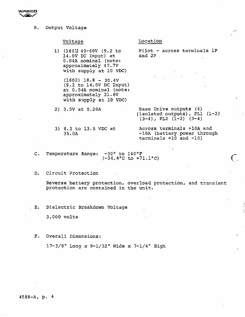
B. Output Voltage
Voltage
1) (1601) 40-60V {9.2 to 14.0V DC Input) at 0.84A nominal (note: approximately 47.7V with supply at 10 VDC)
(1602) 1a.a· - 30.4v (9.2 to 14.0V DC Input) at 0.54A nominal (note: approximately 21.6V with supply at 10 VDC)
2) 3.SV at 0.20A
3) 8.3 to 13.5 VDC at 35.0A
Location
Pilot - across terminals lP and 2P
Base Drive outputs (4) (isolated outputs), PLl (1-2)
(3-4), PL2 (1-2) (3-4)
Across terminals +lOA and -lOA (battery power through terminals +10 and -10)
c. Temperature Range: -30° to 160°F (-34.4°C to +71.1°C)
D. Circuit Protection
Reverse battery protection, overload protection, and transient protection are contained in the unit.
E. Dielectric Breakdown Voltage
3,000 volts
F. Overall Dimensions:
17-3/8" Long x 9-1/32" Wide X· 7-1/4" High
4588-A, p. 4
WABCO ~"""' A. Input
1) Connect the power supply to terminals +10 and -10.
2) If the unit is to be driven by an F-70 Inverter Driver, use terminals lX and 4X for the input.
3) If the unit is to be driven from a pilot line, use terminals lX and 2X for the input, and jumper terminal ·3x to terminal 4X.
B. Output
1) Power for the FS0-2 Inverter Follower is supplied by terminals +lOA and -lOA.
2) A Pilot Line output is supplied by terminals Pl and P2.
3) The FS0-2 Inverter Follower can be driven from cable PLl or PL2.
SECTION V
MAINTENANCE
NOTE
The following test equipment, or equivalent, is recommended for field and shop maintenance and test procedures.
Oscilloscope Voltmeter
Ammeter
Frequency Counter Signal Generator Audio Amplifier D.C. Power Supply
High Pot Tester (2) Resistor Decade Box
4588-A, p. 6
Tektronix Model 502 A.C. HP Model 3400A D.C. Weston Model 622 A.C. 0-250 MA Weston Model 155 D.C. Weston Model 1 ATEC Model 5A35 Wavetek Model 112 Mcintosh SOW 0-14V, 0-SA Harrison Laboratories Model 6266 0-3000V 60 HZ. 1 MA Trip Clarostat Model 240-C
. :~
·~ .. }·
WABCCJ ~
5. 1 FIELD MAINTENANCE (Refer to Figures 2 and 4)
1. Measure the output voltages at PL-1, PL-2, lP and 2P, +lOA and -lOA. These voltages should correspond to those in Section II.
2. Check Fuse Fl. If the fuse is blown, refer to Section VII, Parts List for exact replacement.
3. Test for the DC supply voltage. Refer to Section II for exact specification.
4. Measure the input level. The level should correspond to that in Section II.
5. Visually inspect the unit for the condition of the case, terminals, and wiring.
If service is not restored from the above field maintenance tests, return the unit to the shop for repair.
5.2 SHOP MAINTENANCE (REFER TO FIGURES 2 THROUGH 6)
1. Apply the proper input and connect the unit as specified in Section II.
2. Check Fuse Fl. If the fuse is opened, refer to Section VI, Parts List, for exact replacement. If the fuse is blown, cause should be determined and corrected before replacing the fuse. If the fuse is working properly check the following:
a. The input and output levels should correspond to those in Section II.
b. Measure the DC supply· voltage. This voltage should correspond to that in Section II.
3. Troubleshoot the amplifier stages. While troubleshooting, a square wave should be found throughout the unit.
a. Across capacitor Cl, 16 volts peak to peak should be measured.
b. At the base of Ql and Q2, approximately 1 volt peak to peak should be measured.
c. Across Transformer T2, approximately 20 volts peak to peak should be measured at locations 1P-2P and 3P-4P.
4588-A, p. 7
SECTION III
3.1 GENERAL THEORY
The F-50-1 Inverter Follower Input Stage consists of two switching amplifier stages which amplify a low power input signal to a usable output signal level.
3. 2 DETAILED THEORY (Refer to Figure 2)
WAEICC
""V"•"""
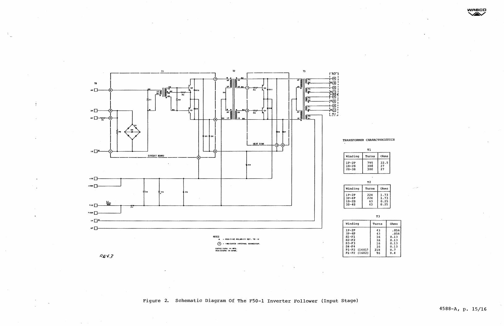
When the Inverter Follower is driven by a Pilot Line Signal, components Rl, R2, Dl, and D2 clip the input at 16 volts peak to peak. This clipper circuit provides input regulation and surge protection for the unit.
Transformer Tl couples the input signal to the first amplifier stage which consists of transistors 01 and 02. Capacitors Cl and C2 broadly tunes transformer Tl to the operating frequency of the unit. Transformer T2 couples the output of the first stage to transistors 03 and 04 which makeup the output stage. Both amplifiers operate as switching amplifiers. The output is coupled through transformer T3 which provides outputs for driving one or two FS0-2 Inverter Follower output stages. Transformer T3 also provides a piiot line output at locations Pl and P2.
Zener Diode D4 and diodes DS through Dl2 provide transient surge protection for transistors Ol through 04. Choke Ll and capacitor C3 and C4 filter the battery voltage, providing surge suppression for both the FS0-1 and the FS0-2 (connected at +lOA and -lOA) units. Fuse Fl provides overload protection, and diode D3 provides reverse battery protection.
SECTION IV
INSTALLATION (REFER TO FIGURE 2 AND 4)
The installation of the FS0-1 Inverter Follower consists of the following:
NOTE
Refer to Section II for the Input and Output signal specifications required for this unit.
4588-A, p. 5
WABCC 'V'"•~
d. The base of Q3 and Q4 should measure approximately 1 volt peak to peak.
e. Across Transformer T3, approximately 20 volts peak to peak should be measured at locations 1P-2P and 3P-4P.
f. Measure the output at PLl, PL2, and lP and 2P. Refer to Section II for output voltage specifications for open circuit output voltages, Refer to Section 5.3.
5.3 TEST PROCEDURE
To test the units, use the following procedures.
NOTE
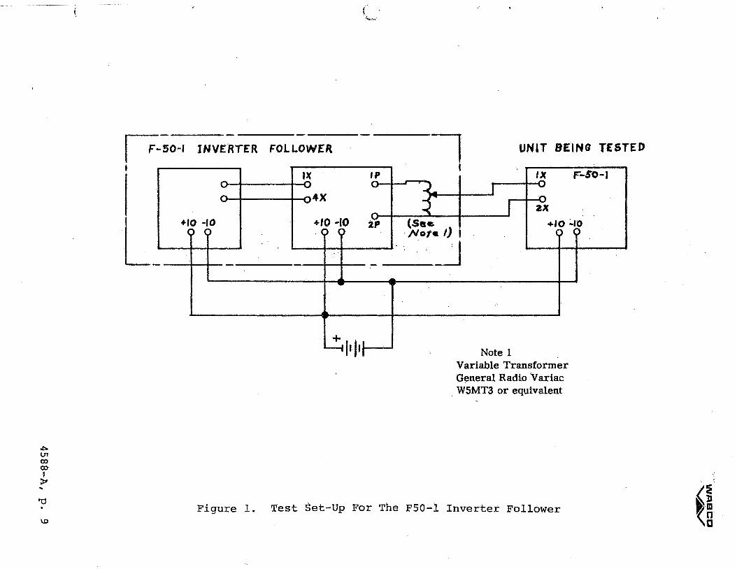
Refer to Figure 1 for the FS0-1 test set-up. If the unit 1601 (83. 3Hz.) is to be tested, a spare.style F70 Inverter Driver (UN451034-6302, 83. 3 Hz.); style FS0-1 Inverter Follower (UN451033-1601. 83. 3Hz.); and a variable transformer {General Radio Varic WSMT3 or equivalent) should be used to supply the 83.3 Hz square wave power required for testing.
If the unit 1602 (100 Hz.) is to be tested, substitute style F70 Inverter Driver. UN451034-6303 (100 Hz.) and style FS0-1 Inverter Follower UN451033-1602 (100 Hz.) for the above.
1. High Level Input Test (No DC Power Applied)
(Do NOT connect battery to +10 and -10 terminal of unit being tested).
a. Remove Jumper 3X to 4X
NOTE
When testing Unit 1601, proceed with Steps B & c. When testing Unit 1602, proceed with Steps D & E.
b. With ohmmeter check Rl at 500 ohms ±5% (test 2X-3X). With ohmmeter check R2 at 150 ohms ±5% (test 1X-3X). Apply 20.0 volts 83.3 Hz (square wave) to lX and 2X and measure voltage lX to 3X between 4.2 volts and 5.0 volts AC with calibrated oscilloscope.
4588-A, p. 8
.e:. 01 0) 0)
I ~
to . \.0
! '· ,.,1,.·.~
~so-, INVERTER FOLLOWER
I •!
,, ..... ..., u \., o4X
+IO -10 +IO -10 I..,,
2P ) ) . I) ! )
. .
- -L_
+ 1--1 laf 11
..
I UNIT BEING TESTED I
IX F-50-1 - t I J -I -, 1'\ ... , I
..... ~ .. 2X
(See. · Not• I) I
+lo :..,_,o (') I)
J
-- .
Variable Transformer General Radio Variac W5MT3 or equivalent
Figure 1. Test Set-Up For The FS0-1 Inverter Follower ,1 ~8
WABCO """~ c. Apply 45.0V, 83.3 Hz {square wave) to lX and
2X. Note that the voltage across lX and 3X is between 6.6 and 8.6V AC, as measured with a calibrated oscilloscope. If the positive and negative half cycles of the square wave are not symmetrical the diode bridge 01 is faulty and should be replaced. If the magnitude is not between 6.6 and 8.6 volts the Zener diode 02 should be replaced. Proceed with Step F.
d. With ohmmeter check Rl at 100 ohms ±5% (test 2X-3X)~ With ohmmeter check R2 at 150 ohms ±5% (test 1X-3X). Apply 20.0 Volts 100 Hz {square wave) to lX and 2X and measure voltage lX to 3X between 5.8 volts and 7.1 volts AC with calibrated oscilloscope.
e. Apply 15.0V, lOOHz (square wave) to lX and 2X. Note that the voltage across lX and 3X is between 5.8 and 7.lV AC, as measured with a calibrated oscilloscope. If the positive and negative half cycles of the square wave are not symmetrical the diode bridge 01 is faulty and should be replaced. If the magnitude is not between 5.8 and 7.1 volts the Zener.diode 02 should be replaced.
f. With power applied as per Step "C", place a jumper across 3X and 4X. Observe that base current is being applied to'Ql and Q2. The base current shall fall between 0.013 and O.OlaA·as "determined by the voltage drop across R3. (1.3 volt.to 1.8 volt). Check with calibrated oscilloscope or with 20,000 ohms/volt DC meter.
2. With input energized per Item 1, apply 10 VDC to terminals +10 and -10 through a O.SA fuse (or equivalent). This energizes transformers T2 and T3.
a. If transformers Tl or T2 have been replaced, color code must be observed.
b. Base current of Q3 and Q4 will be approximately 0.36A (during conducting half cycle). Check.with calibrated oscilloscope. { 1. av across R4 and RS} •
c. The DC Input current should be approximately 0.3A.
45 88-A, p. 10
Note: If any of the diodes D3 through 08 are reversed or improper base phasing exists due to improper transformer connection. The O.SA fuse will open.
d. Open Circuit Output Voltages 1601 1602
WAEICCJ ~
lP - 2P = 49 VAC #1 to #2 = 3.6 VAC
PLl and PL2 (each) #3 to #4 = 3 • 6 VAC +lOA to -lOA = 10.0V DC
l~ - 2P = 22.4 VAC #1 to #2 = 3.6 VAC #3 to #4 = 3.6 VAC
+lOA to -lOA = 10.0V DC
3. Phase Check of Output Sockets
Jumper pins #2 and #3 and read voltage between #1 and #4. In each case the voltage shall be 7.2V AC.
f. Phasing Test
Jumper Pins 3 & 2 of PLl Jumper Pins 3 & 2 of PL2 Jumper Pin 4 of PLl to Pin 1 of PL2 Jumper 2P to Pin 1 of PLl Jumper 4X to lP
(1601} The voltage between lX and pin #4 of PL2 should be between 66 and 76 VAC at 10 VDC input.
(1602) The voltage between IX.and pin #4 of PL2 should be between 40 and 48 VAC at 10 VDC input.
I NOTE ,;;.,
All units MUST be identical in regard to instantaiieous polarity.
g. Check waveform across the primary of each transformer. The waveform in each case shall be a symmetrical square wave with not more than 2V transient at the leading edge.
3. Final Tests
A. Load as follows: (1601)
(a) Apply 45.0V 83.3 Hz (square wave) to terminals lX and 2X with a jumper across 3X and 4X.
(b) Apply 10 VDC to +10 and -10 terminals (approximately 6A capacity).
(c) Connect 60 ohm, 50 watt resistor to lP and 2P. Connect 175 ohm 1 watt resistor to PLl terminals
1 and 2. Connect 175 ohm 1 watt resistor to PL2 terminals
l and 2.
IDC = 4.2 amps. approximately +1P-2P = 47.4V approximately
4588-A, p. 11
#1 and #2 or #3 and #4 = 3.SV approximately {using either PLl or PL2)
(d) Check waveforms across transformer secondaries noting that they are essentially square wave and symmetrical.
B. Load as follows: (1602)
a. Apply 15.0V 100 Hz (square wave) to terminals lX and 2X with a jumper acros.s 3X an 4X.
b. Apply 10 voe to +10 and -10 terminals· (approximately 6A_capacity).
c. Jumper Pins 2 and 3 of PLl Jumper Pins 2 .and 3 of PL2 Jumper Pin 4 of P~l to Pin l of PL2
d. Connect 40 ohm, 25 watt resistor to lP and 2P. Connect 600 ohm, ·1 watt resistor to PLl
terminal 1 ·.and PL2 terminal 4.
IDC. = 1.58 a~ps approximately +1P-2P = 21. 9.V app_roximately PLl-1 and PL2-4 = 1·4. 7V approximately
e. Check waveforms across transformer secondaries noting that they are essentially square wave and symmetrical.
SECTION VI
PAR'rs LIST
7.1 Replacement parts for the FS0-1 Inverter Follower (input stage) either 1601 or 1602 may be ordered directly from WABCO Union Switch & Signal Division, Swissvale, Pa., by specifying the part number and description.
7.2 This parts list covers the Inverter Follower (input stage) models 1601 and 1602.
4588-A, P· 12
FS0-1
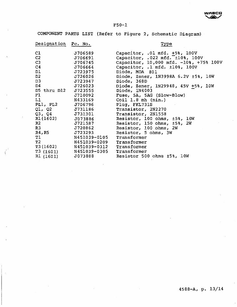
WABCD ~""' COMPONENT PARTS LIST (Refer to Figure 2, Schematic Diagram)
Designation
Cl C2 C3 C4 Dl 02 03 04 05 thru 012 Fl Ll PLl, PL2 Ql, Q2 Q3, Q4 R1{1602) R2 R3 R4,R5 Tl T2 T3(1602) T3 (1601) Rl (1601)
Pc. No.
J706589 J706691 J706745 J706664 J723975 J726026 J723947 J726023 J723555 J710092 N433169 J706796 J731186 J731301 J073886 J721587 J720862 J723293 N451039-0105 N451039-0209 N451039-0312 N451039-0305 J073888
Capacitor, .01 mfd. +5%, lOOV Capacitor, .022 mfd.-±10%, lOOV Capacitor, 10,000 mfd. -10%, +75% lOOV Capacitor, .1 mfd. ±10%, lOOV Diode, MDA 801 Diode, Zener, 1N3998A 6.2V ±5%, lOW Diode, 3680 Diode, Zener, 1N29948, 45V +5%, lOW Diode, 1N4003 -Fuse, SA, SAG (Slow-Blow) Coil 1.8 mh (min.) Plug, FKL731S Transistor, 2N2270 Transistor, 2Nl558 Resistor, 100 ohms, ±5%, lOW Resistor, 150 ohms, ±5%, 2W Resistor, 100 ohms, 2W Resistor, 5 ohms, 3W Transformer Transformer Transformer Transformer Resistor 500 ohms ±5%, lOW
4588-A, p. 13/14
TB
4X
•• 1¥
••
IX ...,._~~1)--4-----+---~
-10
-teA
+10
+toA
.. . tr
L---------~~---------rs,--
!.!,_
Fl
Rfi\/J
04 c, +
o,
T2 ,-_-_ -_ I
••
I I L.!Jlli_S.!!!L
o,
IOTES e - POSITIVE POLAltlTY REF. TO IX
© - INOICATCS INTERNAL CONNECTOR.
CAPACITORS IN MFO, RESISTORS IN OHMS.
011
I , I ,-•3)-{41J
T3 fPt:Z-1 I I ~'~;-=-----:,-. ~ : l~: fir, 12 t
'°I' •• I I h--:f ~,-;~:-----11--. ~ ! ~,: !,~ l
L~~
TRANSFORMER CHARACTERISTICS
Tl
Winding Turns Ohms
1P-2P 795 22.5 1s-2s 30d 27 2S-3S 30d 27
T2
Winding Turns Ohms
1P-2P 224 1. 73 3P-4P 224 1. 73 1S-2S 63 0.25 3S-4S 63 0.25
T3
Winding Turns Ohms
1P-2P 43 .056 3P-4P 43 .056 Sl-Fl 16 0.13 S2-F2 16 0.13 S3-F3 16 0.13 S4-F4 16 0.13 Pl-P2 (1601) 218 0.7 Pl-P2 (1602) 96 0.4
Figure 2. Schematic Diagram Of The FS0-1 Inverter Follower (Input Stage)
WABCO ~
4588-A, p. 15/16
---.... ·
J"Ut,flPERS
*10 G:?EEN -(TB-JO TO T8-IOAJ
r.:::r--, TB-IP-,.185
l~J-!! __ hs-zP _ .. ,se
Hf,tT :;/Nie s, ~ ~ ?!; ci.io -"' 'f"' i· ~#
-!-
Q' ~ + +
~~~
I
2
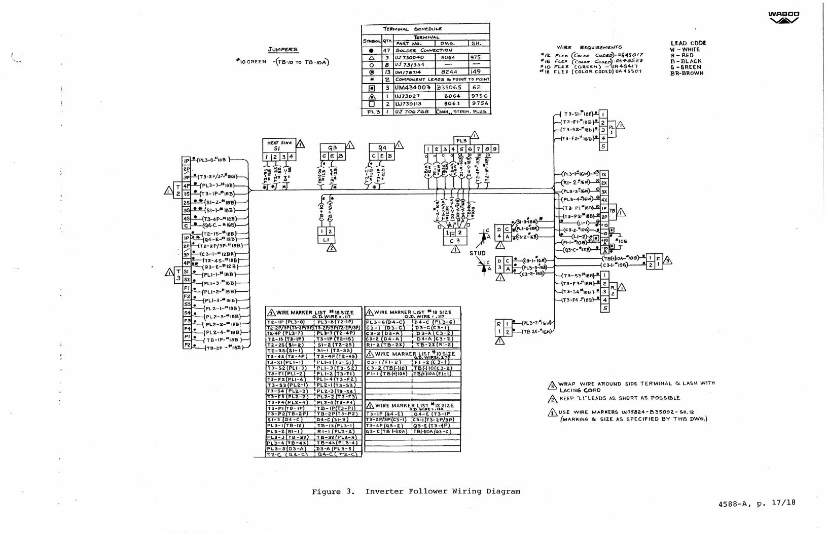
&_WIRE MARKER LIST :1$18 SIZE O. D, WIRE.•, 117
T2.-IP (PL3-B) I PL3-8(T2.-IP) T2.-2.P /3Pl T3·2. P/3PJ:T3-2P/3PIT2.·2.P /3P) T2.-4P { PL3-7 J P\.3•7 (T2.-4PJ T2.-IS (T3-IP) T3-IP (T2.-IS) T2.-2.S(Sl-2.} ! SI- 2. (T2-2.S) T2.-3S{SI- I} I SI-I (T2.-3S} T2-4S(T3-4P) I T3-4P(T2.-4S) T3-Sl(PLI-I} 1 PLI-II T3-Sll T3-S2 PLl-3) I PLl-3 T';!-S 2 > T3-Fl(PLl-2l 1 PLl-2. T3-FI) T3-F2 PLl-4) IPLl-4 T3 -F2.) T3-S3 (PL2.-I • PL2-I T3-5::,,) T3-S4 PLZ-3 'PL2.-3 T3-S4 I T3-F3 PLZ-2 PL2-2 T3-F3\ T3·F41 PL2-4 I PL2-4 T3-F4) T3-PII TB-IP) TB-IP T3-PI) T3-P2. TB-2PJ 1 TB-2P (T3-P2.) Sl-3 fD4-C I D4-C [$1-3) PL3-l(T8-l')(} T8-IY. (PL3· l l PL3-2. Rl-1 l R' 1-1 {PL3-2.) P\.3-3 Te-3')() Tf~-3l( (PL3-3) PL3-4 TB-4'lll TB-41-(PL~-4) PL3-S 03-A) D3-A(PL3-S) 1"2.·C. Q,\.-C.) Q.0,.-C. C T,-C. \
Figure 3.
TERMINAL SCH!!OI.JLE.
5YM80L QTY. TsllMIIIIAL
PAR.1" NO. D\11,G. SH. WlR.E l,?EQU12EM!!IJ1"S • 47
L::, 3
0 8 ® /3
SOLDER. Co1'1Nt!.GTJO,J
U:t730040 8064 IJJ°7.3/354 -· IJM/787/4 8244
975 -149
*12. Ft.£>< (Cot..o.e Coo£'?)-tJ(l'ffOl7 #/6 Ft..E:X (CoLoA!' C4 o.:o)·UA45525 it 10 FU X (.Gl:t.EE!i) - UA 4-S4-I? '°"18 FLE)( (COLOR CODED) UA4SS07
llf 2 COHll'Ot,Jf!.IJT LE:ADS lie POINT TO POINT
[!) 3 UM434003
& I UJ73027
0 2 UJ730113
F'L:, I UJ 70t;,7i!o8
~ ~ <.J; Q.11)
I .9 I ('J
rJjj ... ; ,- ,. .... *...__,_~
B3SOGS 62
8064 975C
1)06-t 975A
!."oNN '1)rE~M. ?L.UG.
ex. ,., ..... , -·a.. w,Cfl"o
~ io:", ·~~~ :i;; ~ * ti' ';";!j V .;, ,t- ~It ~Sl-3-18,t) o1 ,.,_ "' f\ A 41' ,
.!. ~tt A pu-,-,e~ u.. " O DC •·
L!\ WIRE MARKER LIST • 1e SIZ.E O,D. WIRE~ , 117
PL3-6(D4-C) lt>4-C {PL3-61 C3- I (D3-C1 : 1)3-C(C3-I\ C3-2{D3-A) , D3-l>dC3-2l C3-2. {04-A) 04-A (C3-'2.) Rl-2.(TB·2.-,.J , TS-2.X \Rl-21
L!\ WIRE MARKEl3._-k!i~ .. 1:~0N1-E. C3-I (Fl-2) !Fl-2.(C3-II c 3-2. (TBC-\10 l TB(-J IO(C3·2.) Fl-I lTE!,(+}IOA) ,TB[+)IOA(Fl-1}
, ~ A C!·Z-"B
ST~
~
3-1-~"".: PL~-5-,ial " . 3-2.-IBB
I
~
PL:.·2-*1,;,w
TB 2X·"11ow: I
T3-Sl~l8Bu
s
U~D cODl W -WHITE R- RE.D B-BLACK G -GREEt-1 B"R-BROWN
I
I
I
& WRAP Wll<E .&."ROUND SIDE TE.RMINAL & LASH WITH
LACIN~ (.ORD
£ KEEP '"Ll"'LEADS AS SHORT AS POSSIBLE. .
& WIRE MAR~~n~J.~.I/.lr.?12.E T3-IP (Q4-E) Q4-E (T3-IP T3-2.P/3P(C:H) C3-l(T3-2.P/3P) T3-4P(Gl3-E\ Q3-E.fT3·4PI Q3- C(TB {-)IOI>-) TB(-}IOA (Gil -c)
Inverter Follower Wiring Diagram
&usE WIRE. MARKERS UJ75824-f:135002.- SH.12.
{MARKING & SIZ.E. A.S SPECIFIED BY THIS DWG.)
WABCO ~
4588-A, p. 17/18
-I" ... CJ>
-1-f
18173
T'2.
' HEAT ~tlll( i ....i
SI I f- - - - - - - - - - -J
I' J~ r,------ 11 I~·-· ,_T___ _ ... -1
L___ / ---- l_-'-t-t · --~=~ ___ 1-1 -7!..,;A-:.-,_1 --,
r-~-- ...J ' ;+' ---------\---, I ---------,
: + -i_; r1 ------------11 11 I I : I 11
T~ I I I '.i I
' 11 LJ I
1 I I
- - ·-- - - I.J It --,£1 I '--
'-,
'+ I __ \ --
'
LI
'-t• '-,
I
I I I I I I I I
~ +•
·--------L-J I
/ ____ ,
r '"'
5-,
1h 2'5
, IS
-. }
c + - -
l\'Ot:, "TU'oU•o.\Ga 'lr'ULL L.1=."'16"T\.\ O~ "O\O'OILS \t.lC-\..UO\t-.lb \..~A.ll'o.
• ·~-J r- -,
@·~rr ~ -)18! I A- I KEV "i!,o'f "t OM. 'I \~'II...\.
B .---i• ' o~ 9T"2..
• I I
·r Le~
st~! l:Q
,-...~~~-t~~~~-t--~~~~-l-~~~~-11j ~-\"""~~~~-°'<-~~~~.\-~~~~~~~
MTG.PIM.
(i)oR® TOP OF NAME Pl.ATE
au. VJEW .. A"
r.- - -;_1;, __ --: =-=---.;f.: -~ -i----= ~----_-_; _=-_- =-,~.-- --II "
LI
i~VJR .. T ..... ,.,.STG\0
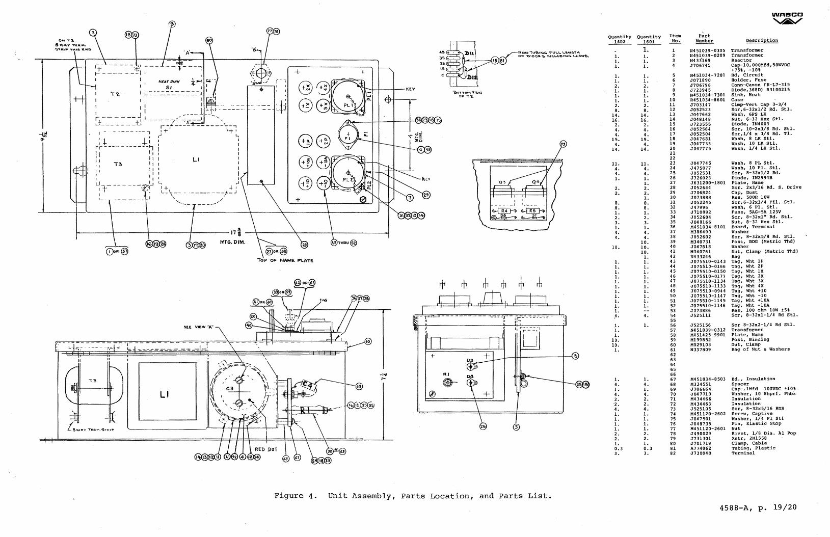
Figure 4.
-1-t i-
rb ~ I
rji rh rjl rh
~?. - 1.----~ - - - ---- - - - '-~- -.1- - Ir - _- - - - - - r .. ,::! •I !'. 1t-,
1, ~;:.··_-.:;1
LJ + .--l- II I I \~
RJ • D~
Ill
5
Unit ~ssembly, Parts Location, and Parts List.
Quantity Quantity Item ~ 1601_ ~
1. 1. 1.
1. 1. 2. 1. 1. 1. 2. 8.
14. 16.
2. 4. 4.
15. 4.
14.
11. 4. 4. 1.
2. 2.
8. 8. 1. 2. 3. 1. 4. 4.
10.
l. 1. 1. l. l. l. l. 1. 1. l. 1. ~. l. l. l.
10. 10. l.
l. 4. l. 4. 2.
·2. 4. l. l. l. 1. 2. 2. l. 0.3 3.
1. 1. 1. 1.
1. 1. 2. 1. 1. 1. 2. 8.
14. 16.
2. 4. 4.
15. 4.
14.
11. 4. 4. 1. 1. 2. 2. 1. 8. 8. 1. 2. 3. 1. 4. 4.
10. 10. 10.
1. 1. l. 1. l. l. l. l. l. l. l. --4.
l.
l. 4. 1. 4. 2. 2. 4. 1. l. 1. l. 2. 2. 1. 0.3 3.
l 2 3 4
5 6 7 8 9
10 11 12 13 14 15 16 17 18 19 20 21 22 23 24 25 26 27 28 29 30 31 32 33 34 35 36 37 38 39 40 41 42 43 44 45 46 47 48 49 50 51 52 53 54 55 56 57 58 59 60 61 62 63 64 65 66 67 68 69 70 71 72 73 74 75 76 77 78 79 80 81 82
' Part ~
N4 51039-0305 N451039-0209 N433169 J706745
N451034-720l J071890 J706796 J723945 N451034-7301 R451034-8601 J703147 J052523 J047662 J048148 J723555 J052564 J052504 J04 7681 J047733 J047775
J047745 J475077 J05253l J726023 J631200-180l J052644 J706824 J073888 J052245 J47996 J710092 J052604 J048166 M451034-8101 M386490 J052602 M340731 J04 7818 M340761 N4 33246 J075510-0l4 3 J075510-0l66 J075510-0l50 J075510-0l 77 J075510-1134 J075510-1133 J075510-0944 J075510-114 7 J07 5510-114 5 J075510-1146 J073886 J525111
J525156 N451039-0312 M451425-9901 Ml99852 M029103 N337809
M451034-8503 M334551 J706664 J047710 M434466 M434463 J525105 M451120-2602 J047501 J048735 M451120-2601 J490029 J731301 J701719 A774062 J730040
WABCC ~
Description
Transformer Transformer Reactor Cap-10,000Mfd,SOWVDC +75%, -10% Bd, Circuit Holder, Fuse Conn-Canon FK-L7-Jl5 Diode,J68DI R3100215 Sink, Heat case Clmp-Vert Cap 3-3/4 Scr,6-32xl/2 Rd. Stl. Wash, 6PS LK Nut, 6-32 Hex Stl. Diode, IN4003 Ser, 10-2x3/8 Rd. Stl. Scr,1/4 x 3/8 Rd. Tl. Wash, 8 LK Stl. Wash, 10 LK Stl. Wash, 1/4 LK Stl.
Wash, 8 PL Stl. Wash, 10 Pl. Stl. Ser, 8-32xl/2 Rd. Diode, IN2994B Plate, Name Ser. 2x3/16 Rd. S. Drive Cap, Dust Res, soon 1ow Scr,6-32x3/4 Fil. Stl. wash, 6 Pl. Stl. Fuse, SAG-SA 125V Ser, 8-32xl" Rd. Stl. Nut, 8-32 Hex Stl. Board, Terminal Washer Ser, 8-32x5/8 Rd. Stl. Post, BOG (Metric Thd) Washer Nut, Clamp (Metric Thd) Bag Tag, Wht lP Tag, Wht 2P Tag, Wht lX Tag, Wht 2X Tag, Wht 3X Tag, Wht 4X Tag, Wht +10 Tag, Wht -10 Tag, Wht +lOA Tag, Wht -lOA Res, 100 ohm lOW ±5% Ser, 8-32xl-l/4 Rd Stl.
Ser 8-32x2-l/4 Rd Stl. Transformer Plate, Name Post, Binding Nut, Clamp Bag of Nut & Washers
Bd., Insulation Spacer Cap-.lMfd lOOVDC ±10% Washer, 10 Shprf. Phbz Insulation Insulation Ser, 8-32x5/16 RDS Screw, Captive Washer, 1/4 Pl Stl Pin, Elastic Stop Nut Rivet, 1/8 Dia. Al Pop Xstr, 2Nl558 Clamp, Cable Tubing, Plastic Terminal
4588-A, p. 19/20
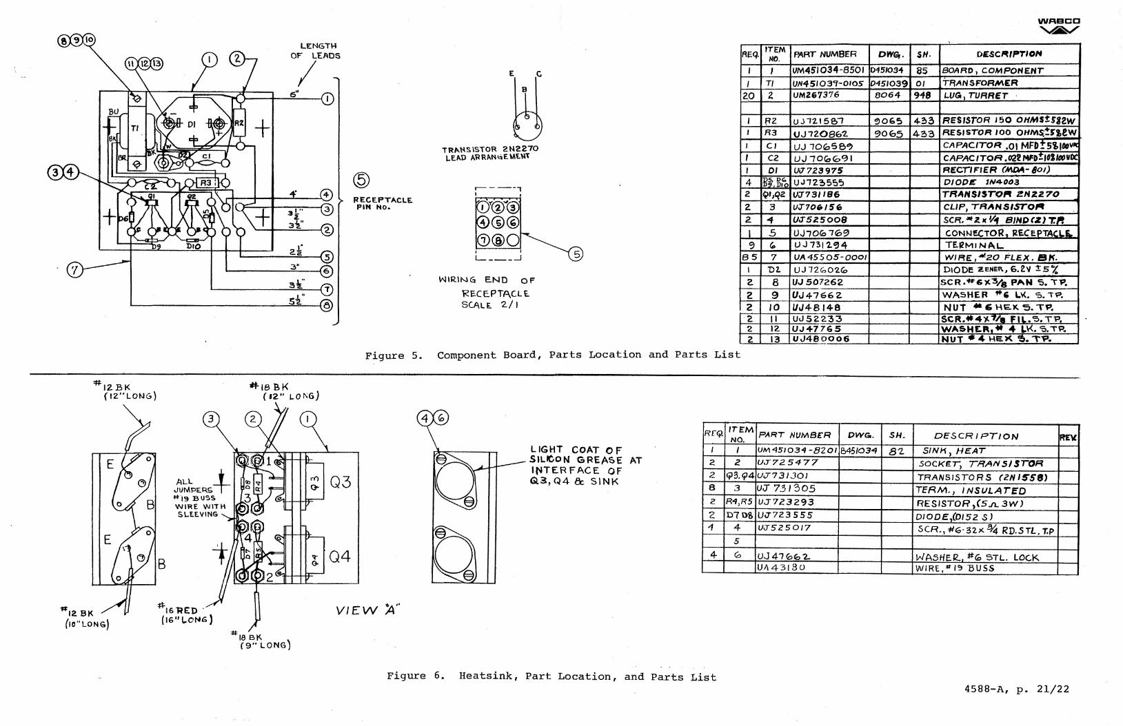
#12BK ( 12" LONG)
""12. BK (IO"LONG}
B
ALL f .JUMPEA.51 *'"19 BUSS WIRE WliH SLEEVING
:f:1:16 ~ED · (IG"LONG)
LENGTH OF LEADS
I e;'
3L" 2.
3~·
.!." 22.
3•
:sf' sf'
@ ~ECEPTACLE. PIH No.
E C I
B
TR,.._NS\STOR 2M2270 1-El>.D A'RRl>.N~E )AU<lT
.--·---, I I I. c _, ' -• < _I
I I L_ ___ ..J
WIRING ENO OF
RE.CE PTA.CLE. SCALE. 2/ I
RE;:q.
I
I
2.0
I I
I
I I 4 2
2. 2
I 9
85
I
2.
2 2 2. 2 2
ITEM PART NUMBER DWG,. NO.
I VM451034-850 I 045103-i
Tl UN45103Cf-OI05 0451039
2 UM267376 8064
R2 uJi215Bt ~OG5 R3 UJ72086'2. '?)065 Cl uJ 100sec:, C2 UJ 10(o~9 I DI Uv723975
B~ O', Din UJ1'2.~515':> 9,,qz U'J731 l86
3 UJ'701#/ 56 .., UJSZ.5008
5 UJ70(o 76'?)
'" UJ7'3t'2.,4 7 UA45505-000I
1)2. UJ 12<,:,0'2.lo
8 UJ501262
9 UJ47662. 10 UJ48148 11 Uu522.'33 12 UJ4-7765 13 UJ480006
Figure 5. Component Board, Parts Location and Parts List
#-18 BK (12" L.01'6)
~103
04
VIEW :A''
#18 BK (9" LONG)
LIGHT COAT OF SILICiON GREA'SE AT ll'JTERFACE OF G.3,Q4 &:. SINK
Rr<;.
I
2
2
8
2
2 1
4
Figure 6. Heatsink, Part Location, and Parts List
IT£M PART NUMBER DWG. SH.
NO.
I U/11\451034 -8201 B45I034 81. 2 U.T72 5477
<?3.94 UJ73/301
3 UJ" 73 I 305 R4,R5 UJ'723293
D?O& UJ723555
4 UJ"52 5017
5 (o UJ 410to"2..
U/\43180
WABCO ~
SH. DESCRIPTION
65 BOARD, COMPONENT
01 TRANSFORMER
918 LUG I TURRET ·
4:>3 RESISTOR 150 OHMSt5J2W
433 RESISTOR 100 OHM~!s,ew CAPACITOR .01 MFD!SIIOOVIII CAPACITOR .022NFD!IOJl«>VOC RECTIFIER (MM-801)
0/00E 1N4003
TRANSISTOl't 1!HZZ70
CLIP, TRAHSISTOfll
SCR, • Z. K Vi BJNP <Z} T.'f CONNECTOR, ~ECE.PTArL£... TE.!2MIN~L.
WIRE ,'*20 FLEX. 191(. DIODE i!.ENER., 6.2'1 !:S"7o
SCR .#6)(3/8 PAN S. ,l'. WASHER *& L'I<. s. ,'P. NUT • g HE.KS. Tl'. SCR.•4~ 7/11 FIL. s. TP. WASHE.I\, tt 4 L\<. s. ,P .. NUT • 4 HE.X ~. 'T'P.
DES CR I PT/ON REV $/NH> HEAT
SOCKET, TRAN SI $TOR
TRANSISTORS (ZN ISS8) TEAM., INSULATED
RESISTOR ,(5.JL 3W)
DIODE,(Dl52 S)
SCR., #6·32>< ·94 RD.STL, T.P
WA5HE.f2., #G STL. LOC.K WIRE,sr 19 13USS
4588-A, p. 21/22