Embed Size (px)
Citation preview
MC56F8455XMC56F8455X / MC56F8454XSupports the 56F84553VLH,56F84550VLF, 56F84543VLH,56F84540VLFFeatures• This family of digital signal controllers (DSCs) is
based on the 32-bit 56800EX core. Each devicecombines, on a single chip, the processing power of aDSP and the functionality of an MCU with a flexibleset of peripherals to support many target applications:– Industrial control– Home appliances– Smart sensors– Fire and security systems– Switched-mode power supply and power
management– Uninterruptible Power Supply (UPS)– Solar and wind power generator– Power metering– Motor control (ACIM, BLDC, PMSM, SR, stepper)– Handheld power tools– Circuit breaker– Medical device/equipment– Instrumentation– Lighting
• DSC based on 32-bit 56800EX core– Up to 80 MIPS at 80 MHz core frequency– DSP and MCU functionality in a unified, C-efficient
architecture
• On-chip memory– Up to 128 KB (96 KB + 32 KB) flash memory,
including up to 32 KB FlexNVM– Up to 16 KB RAM– Up to 2 KB FlexRAM with EEE capability– 80 MHz program execution from both internal flash
memory and RAM– On-chip flash memory and RAM can be mapped
into both program and data memory spaces
• Analog– Two high-speed, 8-channel, 12-bit ADCs with
dynamic x2, x4 programmable amplifier– One 20-channel, 16-bit ADC– Up to four analog comparators with integrated 6-bit
DAC references– One 12-bit DAC
• PWMs and timers– One eFlexPWM module with up to 9 PWM outputs,
including 8 channels with high resolution NanoEdgeplacement
– Two 16-bit quad timer (2 x 4 16-bit timers)– Two Periodic Interval Timers (PITs)– Two Programmable Delay Blocks (PDBs)
• Communication interfaces– Two high-speed queued SCI (QSCI) modules with
LIN slave functionality– Two queued SPI (QSPI) modules– Two SMBus-compatible I2C ports– One flexible controller area network (FlexCAN)
module
• Security and integrity– Cyclic Redundancy Check (CRC) generator– Computer operating properly (COP) watchdog– External Watchdog Monitor (EWM)
• Clocks– Two on-chip relaxation oscillators: 8 MHz (400 kHz
at standby mode) and 32 kHz– Crystal / resonator oscillator
• System– DMA controller– Integrated power-on reset (POR) and low-voltage
interrupt (LVI) and brown-out reset module– Inter-module crossbar connection– JTAG/enhanced on-chip emulation (EOnCE) for
unobtrusive, real-time debugging
Freescale Semiconductor Document Number: MC56F8455X
Data Sheet: Technical Data Rev. 3, 06/2014
Freescale reserves the right to change the detail specifications as may berequired to permit improvements in the design of its products.
© 2014 Freescale Semiconductor, Inc.

• Operating characteristics– Single supply: 3.0 V to 3.6 V– 5 V–tolerant I/O (except RESETB pin)
• LQFP packages:– 48-pin– 64-pin
MC56F8455X / MC56F8454X Data Sheet, Rev. 3, 06/2014.
2 Freescale Semiconductor, Inc.

Table of Contents
1 Overview.................................................................................4
1.1 MC56F844xx/5xx/7xx product family............................4
1.2 56800EX 32-bit Digital Signal Controller (DSC) core....5
1.3 Operation parameters...................................................6
1.4 On-chip memory and memory protection......................6
1.5 Interrupt Controller........................................................7
1.6 Peripheral highlights......................................................7
1.7 Block diagrams..............................................................13
2 MC56F8455x signal and pin descriptions...............................16
3 Signal groups..........................................................................26
4 Ordering parts.........................................................................27
4.1 Determining valid orderable parts.................................27
5 Part identification.....................................................................27
5.1 Description....................................................................27
5.2 Format...........................................................................27
5.3 Fields.............................................................................28
5.4 Example........................................................................28
6 Terminology and guidelines....................................................28
6.1 Definition: Operating requirement.................................28
6.2 Definition: Operating behavior.......................................29
6.3 Definition: Attribute........................................................29
6.4 Definition: Rating...........................................................30
6.5 Result of exceeding a rating..........................................30
6.6 Relationship between ratings and operating
requirements.................................................................30
6.7 Guidelines for ratings and operating requirements.......31
6.8 Definition: Typical value................................................31
6.9 Typical value conditions................................................32
7 Ratings....................................................................................33
7.1 Thermal handling ratings...............................................33
7.2 Moisture handling ratings..............................................33
7.3 ESD handling ratings.....................................................33
7.4 Voltage and current operating ratings...........................34
8 General...................................................................................35
8.1 General characteristics..................................................35
8.2 AC electrical characteristics..........................................35
8.3 Nonswitching electrical specifications...........................36
8.4 Switching specifications................................................42
8.5 Thermal specifications...................................................43
9 Peripheral operating requirements and behaviors..................44
9.1 Core modules................................................................44
9.2 System modules............................................................46
9.3 Clock modules...............................................................46
9.4 Memories and memory interfaces.................................49
9.5 Analog...........................................................................52
9.6 PWMs and timers..........................................................61
9.7 Communication interfaces.............................................62
10 Design Considerations............................................................68
10.1 Thermal design considerations.....................................68
10.2 Electrical design considerations....................................70
11 Obtaining package dimensions...............................................71
12 Pinout......................................................................................72
12.1 Signal Multiplexing and Pin Assignments......................72
12.2 Pinout diagrams............................................................74
13 Product documentation...........................................................77
14 Revision history.......................................................................77
MC56F8455X / MC56F8454X Data Sheet, Rev. 3, 06/2014.
Freescale Semiconductor, Inc. 3
Overview
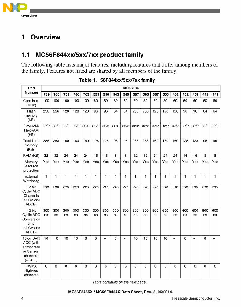
1.1 MC56F844xx/5xx/7xx product family
The following table lists major features, including features that differ among members ofthe family. Features not listed are shared by all members of the family.
Table 1. 56F844xx/5xx/7xx family
PartNumber
MC56F84
789 786 769 766 763 553 550 543 540 587 585 567 565 462 452 451 442 441
Core freq.(MHz)
100 100 100 100 100 80 80 80 80 80 80 80 80 60 60 60 60 60
Flashmemory
(KB)
256 256 128 128 128 96 96 64 64 256 256 128 128 128 96 96 64 64
FlevNVM/FlexRAM
(KB)
32/2 32/2 32/2 32/2 32/2 32/2 32/2 32/2 32/2 32/2 32/2 32/2 32/2 32/2 32/2 32/2 32/2 32/2
Total flashmemory
(KB)1
288 288 160 160 160 128 128 96 96 288 288 160 160 160 128 128 96 96
RAM (KB) 32 32 24 24 24 16 16 8 8 32 32 24 24 24 16 16 8 8
Memoryresourceprotection
Yes Yes Yes Yes Yes Yes Yes Yes Yes Yes Yes Yes Yes Yes Yes Yes Yes Yes
ExternalWatchdog
1 1 1 1 1 1 1 1 1 1 1 1 1 1 1 1 1 1
12-bitCyclic ADCChannels
(ADCA andADCB)
2x8 2x8 2x8 2x8 2x8 2x8 2x5 2x8 2x5 2x8 2x8 2x8 2x8 2x8 2x8 2x5 2x8 2x5
12-bitCyclic ADCConversion
time(ADCA and
ADCB)
300ns
300ns
300ns
300ns
300ns
300ns
300ns
300ns
300ns
600ns
600ns
600ns
600ns
600ns
600ns
600ns
600ns
600ns
16-bit SARADC (withTemperature Sensor)channels(ADCC)
16 10 16 10 8 8 8 16 10 16 10 8 8
PWMAHigh-reschannels
8 8 8 8 8 8 6 8 6 0 0 0 0 0 0 0 0 0
Table continues on the next page...
1
Overview
MC56F8455X / MC56F8454X Data Sheet, Rev. 3, 06/2014.
4 Freescale Semiconductor, Inc.
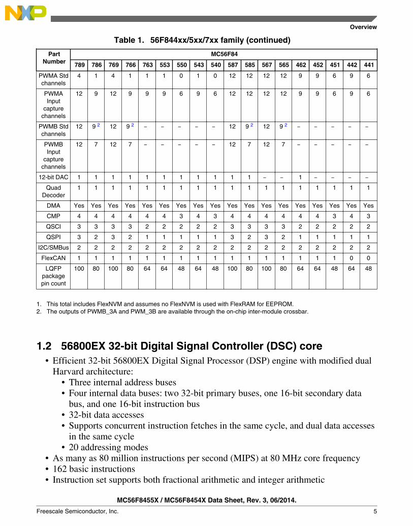
Table 1. 56F844xx/5xx/7xx family (continued)
PartNumber
MC56F84
789 786 769 766 763 553 550 543 540 587 585 567 565 462 452 451 442 441
PWMA Stdchannels
4 1 4 1 1 1 0 1 0 12 12 12 12 9 9 6 9 6
PWMAInput
capturechannels
12 9 12 9 9 9 6 9 6 12 12 12 12 9 9 6 9 6
PWMB Stdchannels
12 9 2 12 9 2 12 9 2 12 9 2
PWMBInput
capturechannels
12 7 12 7 12 7 12 7
12-bit DAC 1 1 1 1 1 1 1 1 1 1 1 1 Quad
Decoder1 1 1 1 1 1 1 1 1 1 1 1 1 1 1 1 1 1
DMA Yes Yes Yes Yes Yes Yes Yes Yes Yes Yes Yes Yes Yes Yes Yes Yes Yes Yes
CMP 4 4 4 4 4 4 3 4 3 4 4 4 4 4 4 3 4 3
QSCI 3 3 3 3 2 2 2 2 2 3 3 3 3 2 2 2 2 2
QSPI 3 2 3 2 1 1 1 1 1 3 2 3 2 1 1 1 1 1
I2C/SMBus 2 2 2 2 2 2 2 2 2 2 2 2 2 2 2 2 2 2
FlexCAN 1 1 1 1 1 1 1 1 1 1 1 1 1 1 1 1 0 0
LQFPpackagepin count
100 80 100 80 64 64 48 64 48 100 80 100 80 64 64 48 64 48
1. This total includes FlexNVM and assumes no FlexNVM is used with FlexRAM for EEPROM.2. The outputs of PWMB_3A and PWM_3B are available through the on-chip inter-module crossbar.
1.2 56800EX 32-bit Digital Signal Controller (DSC) core• Efficient 32-bit 56800EX Digital Signal Processor (DSP) engine with modified dual
Harvard architecture:• Three internal address buses• Four internal data buses: two 32-bit primary buses, one 16-bit secondary data
bus, and one 16-bit instruction bus• 32-bit data accesses• Supports concurrent instruction fetches in the same cycle, and dual data accesses
in the same cycle• 20 addressing modes
• As many as 80 million instructions per second (MIPS) at 80 MHz core frequency• 162 basic instructions• Instruction set supports both fractional arithmetic and integer arithmetic
Overview
MC56F8455X / MC56F8454X Data Sheet, Rev. 3, 06/2014.
Freescale Semiconductor, Inc. 5
• 32-bit internal primary data buses support 8-bit, 16-bit, and 32-bit data movement,plus addition, subtraction, and logical operations
• Single-cycle 16 × 16-bit -> 32-bit and 32 x 32-bit -> 64-bit multiplier-accumulator(MAC) with dual parallel moves
• 32-bit arithmetic and logic multi-bit shifter• Four 36-bit accumulators, including extension bits• Parallel instruction set with unique DSP addressing modes• Hardware DO and REP loops• Bit reverse address mode, which effectively supports DSP and Fast Fourier
Transform algorithms• Full shadowing of the register stack for zero-overhead context saves and restores:
nine shadow registers correspond to nine address registers (R0, R1, R2, R3, R4, R5,N, N3, M01)
• Instruction set supports both DSP and controller functions• Controller-style addressing modes and instructions enable compact code• Enhanced bit manipulation instruction set• Efficient C compiler and local variable support• Software subroutine and interrupt stack, with the stack's depth limited only by
memory• Priority level setting for interrupt levels• JTAG/Enhanced On-Chip Emulation (OnCE) for unobtrusive, real-time debugging
that is independent of processor speed
1.3 Operation parameters• Up to 80 MHz operation at -40 °C to 105 °C ambient temperature• Single 3.3 V power supply• Supply range: VDD - VSS = 2.7 V to 3.6 V, VDDA - VSSA = 2.7 V to 3.6 V
1.4 On-chip memory and memory protection• Modified dual Harvard architecture permits as many as three simultaneous accesses
to program and data memory• Internal flash memory with security and protection to prevent unauthorized access• Memory resource protection (MRP) unit to protect supervisor programs and
resources from user programs• Programming code can reside in flash memory during flash programming• The dual-ported RAM controller supports concurrent instruction fetches and data
accesses, or dual data accesses, by the DSC core.
Overview
MC56F8455X / MC56F8454X Data Sheet, Rev. 3, 06/2014.
6 Freescale Semiconductor, Inc.

• Concurrent accesses provide increased performance.• The data and instruction arrive at the core in the same cycle, reducing latency.
• On-chip memory• Up to 144 KW program/data flash memory, including FlexNVM• Up to 16 KW dual port data/program RAM• Up to 16 KW FlexNVM, which can be used as additional program or data flash
memory• Up to 1 KW FlexRAM, which can be configured as enhanced EEPROM (used in
conjunction with FlexNVM) or used as additional RAM
1.5 Interrupt Controller• Five interrupt priority levels
• Three user-programmable priority levels for each interrupt source: level 0, level1, level 2
• Unmaskable level 3 interrupts include illegal instruction, hardware stackoverflow, misaligned data access, SWI3 instruction
• Interrupt level 3 is highest priority and non-maskable. Its sources include:• Illegal instructions• Hardware stack overflow• SWI instruction• EOnce interrupts• Misaligned data accesses
• Lowest-priority software interrupt: level LP• Support for nested interrupts, so that a higher priority level interrupt request can
interrupt lower priority interrupt subroutine• Masking of interrupt priority level is managed by the 56800EX core• Two programmable fast interrupts that can be assigned to any interrupt source• Notification to System Integration Module (SIM) to restart clock when in wait and
stop states• Ability to relocate interrupt vector table
Peripheral highlights
1.6.1 Enhanced Flex Pulse Width Modulator (eFlexPWM)• One PWM module contains 4 identical submodules, with up to 3 outputs per
submodule, and up to 80 MHz PWM operating clock• 16 bits of resolution for center, edge-aligned, and asymmetrical PWMs
1.6
Peripheral highlights
MC56F8455X / MC56F8454X Data Sheet, Rev. 3, 06/2014.
Freescale Semiconductor, Inc. 7
• PWMA with NanoEdge high resolution• Fractional delay for enhanced resolution of the PWM period and edge placement• Arbitrary PWM edge placement• 390 ps PWM frequency and duty-cycle resolution when NanoEdge functionality
is enabled.• Fractional clock digital dithering: 5-bit digital fractional clock accumulation for
enhanced resolution of PWM period and edge placement, which is effectivelyequivalent to 390 ps resolution in the overall accumulative period.
• PWM outputs can be configured as complementary output pairs or independentoutputs
• Dedicated time-base counter with period and frequency control per submodule• Independent top and bottom deadtime insertion for each complementary pair• Independent control of both edges of each PWM output• Enhanced input capture and output compare functionality on each input:
• Channels not used for PWM generation can be used for buffered output comparefunctions.
• Channels not used for PWM generation can be used for input capture functions.• Enhanced dual edge capture functionality
• Synchronization of submodule to external hardware (or other PWM) is supported.• Double-buffered PWM registers
• Integral reload rates from 1 to 16• Half-cycle reload capability
• Multiple output trigger events can be generated per PWM cycle via hardware.• Support for double-switching PWM outputs• Up to eight fault inputs can be assigned to control multiple PWM outputs
• Programmable filters for fault inputs• Independently programmable PWM output polarity• Individual software control of each PWM output• All outputs can be programmed to change simultaneously via a FORCE_OUT event.• PWMX pin can optionally output a third PWM signal from each submodule• Option to supply the source for each complementary PWM signal pair from any of
the following:• Crossbar module outputs• External ADC input, taking into account values set in ADC high and low limit
registers
1.6.2 12-bit Analog-to-Digital Converter (Cyclic type)• Two independent 12-bit analog-to-digital converters (ADCs):
• 2 x 8-channel external inputs• Built-in x1, x2, x4 programmable gain pre-amplifier
Peripheral highlights
MC56F8455X / MC56F8454X Data Sheet, Rev. 3, 06/2014.
8 Freescale Semiconductor, Inc.
• Maximum ADC clock frequency up to 20 MHz, having period as low as a 50-ns• Single conversion time of 8.5 ADC clock cycles• Additional conversion time of 6 ADC clock cycles
• Support of analog inputs for single-ended and differential conversions• Sequential, parallel, and independent scan mode• First 8 samples have offset, limit and zero-crossing calculation supported• ADC conversions can be synchronized by any module connected to the internal
crossbar module, such as PWM, timer, GPIO, and comparator modules.• Support for simultaneous triggering and software-triggering conversions• Support for a multi-triggering mode with a programmable number of conversions on
each trigger• Each ADC has ability to scan and store up to 8 conversion results.• Current injection protection
1.6.3 Inter-Module Crossbar and AND-OR-INVERT logic• Provides generalized connections between and among on-chip peripherals: ADCs,
12-bit DAC, comparators, quad-timers, eFlexPWMs, PDBs, EWM, and select I/Opins
• User-defined input/output pins for all modules connected to the crossbar• DMA request and interrupt generation from the crossbar• Write-once protection for all registers• AND-OR-INVERT function provides a universal Boolean function generator that
uses a four-term sum-of-products expression, with each product term containing trueor complement values of the four selected inputs (A, B, C, D).
1.6.4 Comparator• Full rail-to-rail comparison range• Support for high and low speed modes• Selectable input source includes external pins and internal DACs• Programmable output polarity• 6-bit programmable DAC as a voltage reference per comparator• Three programmable hysteresis levels• Selectable interrupt on rising-edge, falling-edge, or toggle of a comparator output
1.6.5 12-bit Digital-to-Analog Converter• 12-bit resolution• Powerdown mode
Peripheral highlights
MC56F8455X / MC56F8454X Data Sheet, Rev. 3, 06/2014.
Freescale Semiconductor, Inc. 9
• Automatic mode allows the DAC to automatically generate pre-programmed outputwaveforms, including square, triangle, and sawtooth waveforms (for applications likeslope compensation)
• Programmable period, update rate, and range• Output can be routed to an internal comparator, ADC, or optionally to an off-chip
destination
1.6.6 Quad Timer• Four 16-bit up/down counters, with a programmable prescaler for each counter• Operation modes: edge count, gated count, signed count, capture, compare, PWM,
signal shot, single pulse, pulse string, cascaded, quadrature decode• Programmable input filter• Counting start can be synchronized across counters
1.6.7 Queued Serial Communications Interface (QSCI) modules• Operating clock can be up to two times the CPU operating frequency• Four-word-deep FIFOs available on both transmit and receive buffers• Standard mark/space non-return-to-zero (NRZ) format• 13-bit integer and 3-bit fractional baud rate selection• Full-duplex or single-wire operation• Programmable 8-bit or 9-bit data format• Error detection capability• Two receiver wakeup methods:
• Idle line• Address mark
• 1/16 bit-time noise detection
1.6.8 Queued Serial Peripheral Interface (QSPI) modules• Maximum 25 Mbit/s baud rate• Selectable baud rate clock sources for low baud rate communication• Baud rate as low as Baudrate_Freq_in / 8192• Full-duplex operation• Master and slave modes• Double-buffered operation with separate transmit and receive registers• Four-word-deep FIFOs available on transmit and receive buffers• Programmable length transmissions (2 bits to 16 bits)• Programmable transmit and receive shift order (MSB as first bit transmitted)
Peripheral highlights
MC56F8455X / MC56F8454X Data Sheet, Rev. 3, 06/2014.
10 Freescale Semiconductor, Inc.
1.6.9 Inter-Integrated Circuit (I2C)/System Management Bus (SMBus)modules
• Compatible with I2C bus standard• Support for System Management Bus (SMBus) specification, version 2• Multi-master operation• General call recognition• 10-bit address extension• Start/Repeat and Stop indication flags• Support for dual slave addresses or configuration of a range of slave addresses• Programmable glitch input filter
1.6.10 Flex Controller Area Network (FlexCAN) module• Clock source from PLL or XOSC/CLKIN• Implementation of CAN protocol Version 2.0 A/B• Standard and extended data frames• Data length of 0 to 8 bytes• Programmable bit rate up to 1 Mbps• Support for remote frames• Sixteen Message Buffers: each Message Buffer can be configured as receive or
transmit, and supports standard and extended messages• Individual Rx Mask Registers per Message Buffer• Internal timer for time-stamping of received and transmitted messages• Listen-only mode capability• Programmable loopback mode, supporting self-test operation• Programmable transmission priority scheme: lowest ID, lowest buffer number, or
highest priority• Global network time, synchronized by a specific message• Low power modes, with programmable wakeup on bus activity
1.6.11 Computer Operating Properly (COP) watchdog• Programmable timeout period• Support for operation in all power modes: run mode, wait mode, stop mode• Causes loss of reference reset 128 cycles after loss of reference clock to the PLL is
detected• Selectable reference clock source in support of EN60730 and IEC61508• Selectable clock sources:
• External crystal oscillator/external clock source
Peripheral highlights
MC56F8455X / MC56F8454X Data Sheet, Rev. 3, 06/2014.
Freescale Semiconductor, Inc. 11
• On-chip low-power 32 kHz oscillator• System bus (IPBus up to 80 MHz)• 8 MHz / 400 kHz ROSC
• Support for interrupt triggered when the counter reaches the timeout value
1.6.12 Power supervisor• Power-on reset (POR) to reset CPU, peripherals, and JTAG/EOnCE controllers (VDD
> 2.1 V)• Brownout reset (VDD < 1.9 V)• Critical warn low-voltage interrupt (LVI2.0)• Peripheral low-voltage interrupt (LVI2.7)
1.6.13 Phase-locked loop• Wide programmable output frequency: 240 MHz to 400 MHz• Input reference clock frequency: 8 MHz to 16 MHz• Detection of loss of lock and loss of reference clock• Ability to power down
Clock sources
1.6.14.1 On-chip oscillators• Tunable 8 MHz relaxation oscillator with 400 kHz at standby mode (divide-by-two
output)• 32 kHz low frequency clock as secondary clock source for COP, EWM, PIT
1.6.14.2 Crystal oscillator• Support for both high ESR crystal oscillator (ESR greater than 100 Ω) and ceramic
resonator• Operating frequency: 4–16 MHz
1.6.15 Cyclic Redundancy Check (CRC) generator• Hardware 16/32-bit CRC generator• High-speed hardware CRC calculation• Programmable initial seed value• Programmable 16/32-bit polynomial• Error detection for all single, double, odd, and most multi-bit errors
1.6.14
Clock sources
MC56F8455X / MC56F8454X Data Sheet, Rev. 3, 06/2014.
12 Freescale Semiconductor, Inc.
• Option to transpose input data or output data (CRC result) bitwise or bytewise,1
which is required for certain CRC standards• Option for inversion of final CRC result
1.6.16 General Purpose I/O (GPIO)• 5 V tolerance (except RESETB pin)• Individual control of peripheral mode or GPIO mode for each pin• Programmable push-pull or open drain output• Configurable pullup or pulldown on all input pins• All pins (except JTAG and RESETB) default to be GPIO inputs• 2 mA / 9 mA source/sink capability• Controllable output slew rate
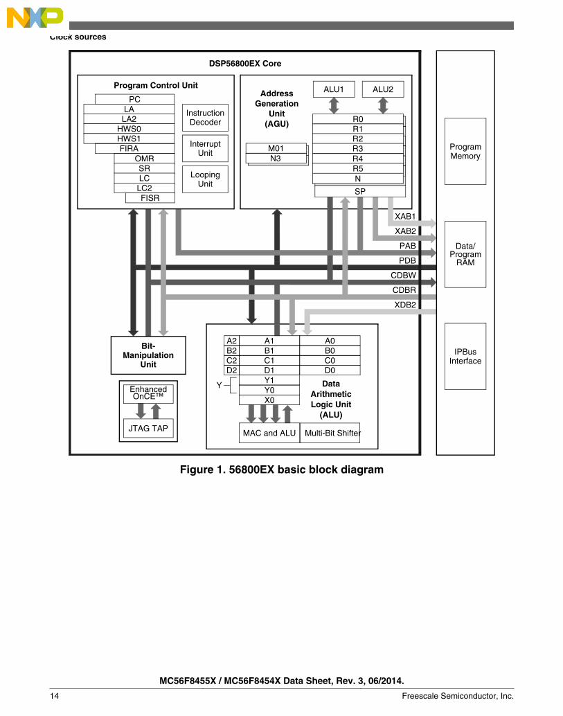
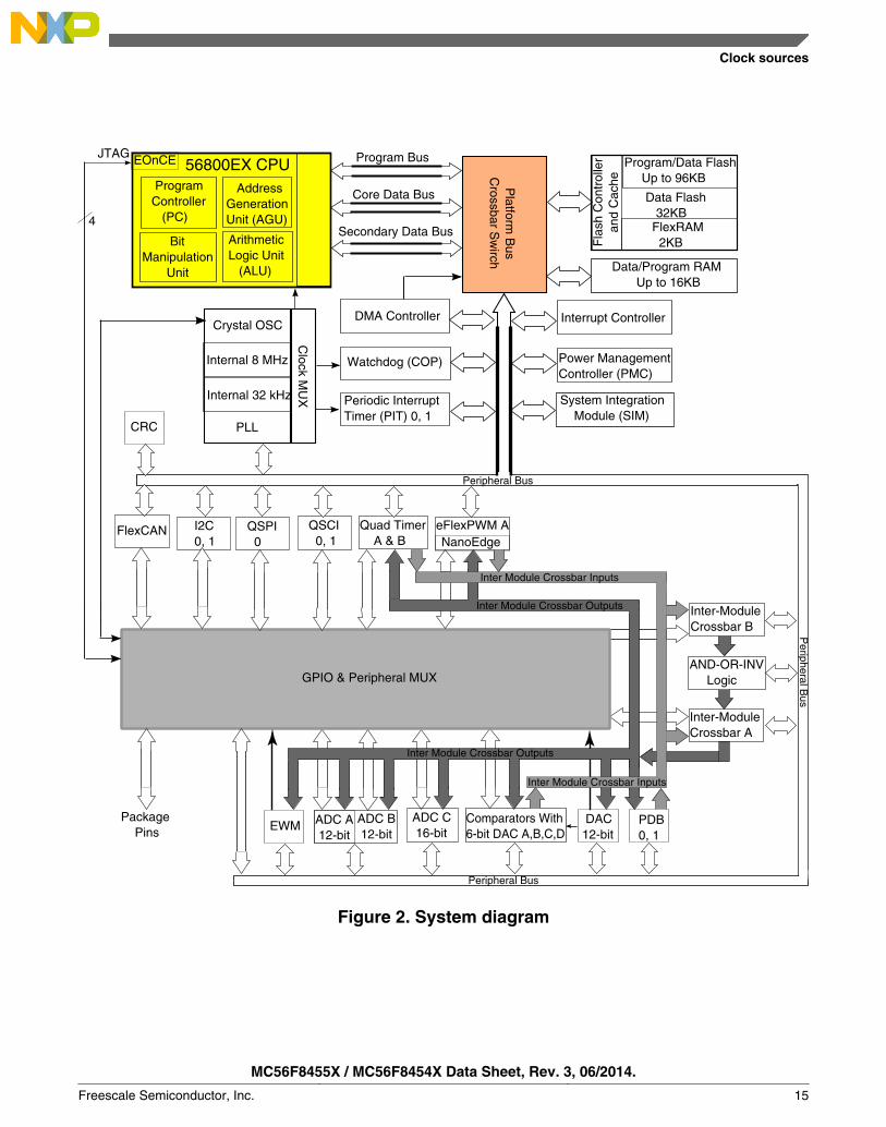
1.7 Block diagrams
The 56800EX core is based on a modified dual Harvard-style architecture, consisting ofthree execution units operating in parallel, and allowing as many as six operations perinstruction cycle. The MCU-style programming model and optimized instruction setenable straightforward generation of efficient and compact code for the DSP and controlfunctions. The instruction set is also efficient for C compilers, to enable rapiddevelopment of optimized control applications.
The device's basic architecture appears in Figure 1 and Figure 2. Figure 1 shows how the56800EX system buses communicate with internal memories, and the IPBus interfaceand the internal connections among the units of the 56800EX core. Figure 2 shows theperipherals and control blocks connected to the IPBus bridge. See the specific device’sReference Manual for details.
1. A bytewise transposition is not possible when accessing the CRC data register via 8-bit accesses. In this case, usersoftware must perform the bytewise transposition.
Clock sources
MC56F8455X / MC56F8454X Data Sheet, Rev. 3, 06/2014.
Freescale Semiconductor, Inc. 13
DataArithmeticLogic Unit
(ALU)
XAB2
PAB
PDB
CDBW
CDBR
XDB2
ProgramMemory
Data/
IPBusInterface
Bit-Manipulation
Unit
M01
Address
XAB1
GenerationUnit
(AGU)
PCLALA2
HWS0HWS1FIRA
OMRSR
FISR
LCLC2
InstructionDecoder
InterruptUnit
LoopingUnit
Program Control Unit ALU1 ALU2
MAC and ALU
A1A2 A0B1B2 B0C1C2 C0D1D2 D0Y1Y0X0
Enhanced
JTAG TAP
R2R3R4R5
SP
R0R1
Y
Multi-Bit Shifter
OnCE™
ProgramRAM
DSP56800EX Core
N3
R2R3R4R5N
Figure 1. 56800EX basic block diagram
Clock sources
MC56F8455X / MC56F8454X Data Sheet, Rev. 3, 06/2014.
14 Freescale Semiconductor, Inc.
Mem
ory Resource
Protection U
nit
EOnCE 56800EX CPU Program Bus
Core Data Bus
Secondary Data Bus
Fla
sh C
ontr
olle
r
and
Cac
he
Program/Data Flash Up to 96KB
Data Flash 32KBFlexRAM 2KB
Data/Program RAM Up to 16KB
DMA Controller Interrupt Controller
FlexCAN QSCI 0, 1
QSPI 0
I2C 0, 1
Quad Timer A & B
Periodic InterruptTimer (PIT) 0, 1
eFlexPWM A NanoEdge
PDB0, 1
ADC A 12-bit
ADC B 12-bit
ADC C 16-bit
Comparators With6-bit DAC A,B,C,D
Watchdog (COP)
EWM
CRC
DAC 12-bit
Inter-ModuleCrossbar B
Inter-ModuleCrossbar A
AND-OR-INV Logic
Inter Module connection
GPIO & Peripheral MUX
Platform
Bus
Crossbar S
wirch
Crystal OSC
Internal 8 MHz
Internal 32 kHz
PLL
Power ManagementController (PMC)
System Integration Module (SIM)
Package Pins
Peripheral Bus
Peripheral Bus
Peripheral B
us
4
JTAG
Inter Module Crossbar Inputs
Inter Module Crossbar Outputs
Clock M
UX
ProgramController (PC)
AddressGenerationUnit (AGU)
ArithmeticLogic Unit (ALU)
BitManipulation Unit
Inter Module Crossbar Outputs
Inter Module Crossbar Inputs
Figure 2. System diagram
Clock sources
MC56F8455X / MC56F8454X Data Sheet, Rev. 3, 06/2014.
Freescale Semiconductor, Inc. 15

2 MC56F8455x signal and pin descriptionsAfter reset, each pin is configured for its primary function (listed first). Any alternativefunctionality, shown in parentheses, must be programmed through the GPIO moduleperipheral enable registers (GPIO_x_PER) and the SIM module GPIO peripheral select(GPSx) registers. All GPIO ports can be individually programmed as an input or output(using bit manipulation).
• There are 2 PWM modules: PWMA, PWMB. Each PWM module has 4 submodules:PWMA has PWMA_0, PWMA_1, PWMA_2, PWMA_3; PWMB has PWMB_0,PWMB_1, PWMB_2, PWMB_3. Each PWM module's submodules have 3 pins (A,B, X) each, with the syntax for the pins being PWMA_0A, PWMA_0B, PWMA_0X,and PWMA_1A, PWMA_1B, PWMA_1X, and so on. Each submodule pin can beconfigured as a PWM output or as a capture input.
• EWM_OUT_B is the output of the External Watchdog Module (EWM), and is activelow (denoted by the "_B" part of the syntax).
For the MC56F8455X products, which use 48-pin LQFP and 64-pin LQFP packages:
Table 2. Signal descriptions
Signal Name 64LQFP
48LQFP
Type StateDuringReset1
Signal Description
VDD 29 - Supply Supply I/O Power — Supplies 3.3 V power to the chip I/O interface.VDD 44 32
VDD 60 44
VSS 30 22 Supply Supply I/O Ground — Provide ground for the device I/Ointerface.VSS 43 31
VSS 61 45
VDDA 22 15 Supply Supply Analog Power — Supplies 3.3 V power to theanalog modules. It must be connected to a cleananalog power supply.
VSSA 23 16 Supply Supply Analog Ground — Supplies an analog ground tothe analog modules. It must be connected to aclean power supply.
VCAP 26 19 On-chipregulatoroutputvoltage
On-chipregulatoroutputvoltage
Connect a 2.2uF or greater bypass capacitorbetween this pin and VSS to stabilize the corevoltage regulator output required for properdevice operation. V<sub>CAP</sub> is used toobserve core voltage.
VCAP 57 43
Table continues on the next page...
MC56F8455x signal and pin descriptions
MC56F8455X / MC56F8454X Data Sheet, Rev. 3, 06/2014.
16 Freescale Semiconductor, Inc.

Table 2. Signal descriptions (continued)
Signal Name 64LQFP
48LQFP
Type StateDuringReset1
Signal Description
TDI 64 48 Input Input,internalpullupenabled
Test Data Input — Provides a serial input datastream to the JTAG/EOnCE port. It is sampledon the rising edge of TCK and has an internalpullup resistor. After reset, the default state isTDI.
(GPIOD0) Input/Output Input,internalpullupenabled
GPIO Port D0
TDO 62 46 Output Output Test Data Output — This tri-stateable pinprovides a serial output data stream from theJTAG/EOnCE port. It is driven in the shift-IR andshift-DR controller states, and it changes on thefalling edge of TCK. After reset, the default stateis TDO.
(GPIOD1) Input/Output Input,internalpullupenabled
GPIO Port D1
TCK 1 1 Input Input,internalpullupenabled
Test Clock Input — This input pin provides agated clock to synchronize the test logic andshift serial data to the JTAG/EOnCE port. Thepin is connected internally to a pullup resistor. ASchmitt-trigger input is used for noise immunity.After reset, the default state is TCK.
(GPIOD2) Input/Output Input,internalpullupenabled
GPIO Port D2
TMS 63 47 Input Input,internalpullupenabled
Test Mode Select Input — Used to sequencethe JTAG TAP controller state machine. It issampled on the rising edge of TCK and has aninternal pullup resistor. After reset, the defaultstate is TMS.
NOTE: Always tie the TMS pin to VDD througha 2.2K resistor, if needed to keep anon-board debug capability. Otherwise,tie the TMS pin directly to VDD.
(GPIOD3) Input/Output Input,internalpullupenabled
GPIO Port D2
Table continues on the next page...
MC56F8455x signal and pin descriptions
MC56F8455X / MC56F8454X Data Sheet, Rev. 3, 06/2014.
Freescale Semiconductor, Inc. 17
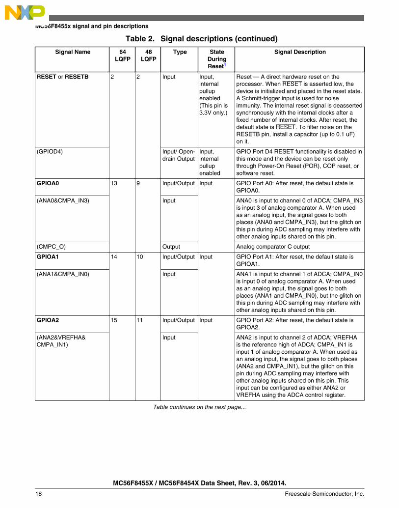
Table 2. Signal descriptions (continued)
Signal Name 64LQFP
48LQFP
Type StateDuringReset1
Signal Description
RESET or RESETB 2 2 Input Input,internalpullupenabled(This pin is3.3V only.)
Reset — A direct hardware reset on theprocessor. When RESET is asserted low, thedevice is initialized and placed in the reset state.A Schmitt-trigger input is used for noiseimmunity. The internal reset signal is deassertedsynchronously with the internal clocks after afixed number of internal clocks. After reset, thedefault state is RESET. To filter noise on theRESETB pin, install a capacitor (up to 0.1 uF)on it.
(GPIOD4) Input/ Open-drain Output
Input,internalpullupenabled
GPIO Port D4 RESET functionality is disabled inthis mode and the device can be reset onlythrough Power-On Reset (POR), COP reset, orsoftware reset.
GPIOA0 13 9 Input/Output Input GPIO Port A0: After reset, the default state isGPIOA0.
(ANA0&CMPA_IN3) Input ANA0 is input to channel 0 of ADCA; CMPA_IN3is input 3 of analog comparator A. When usedas an analog input, the signal goes to bothplaces (ANA0 and CMPA_IN3), but the glitch onthis pin during ADC sampling may interfere withother analog inputs shared on this pin.
(CMPC_O) Output Analog comparator C output
GPIOA1 14 10 Input/Output Input GPIO Port A1: After reset, the default state isGPIOA1.
(ANA1&CMPA_IN0) Input ANA1 is input to channel 1 of ADCA; CMPA_IN0is input 0 of analog comparator A. When usedas an analog input, the signal goes to bothplaces (ANA1 and CMPA_IN0), but the glitch onthis pin during ADC sampling may interfere withother analog inputs shared on this pin.
GPIOA2 15 11 Input/Output Input GPIO Port A2: After reset, the default state isGPIOA2.
(ANA2&VREFHA&CMPA_IN1)
Input ANA2 is input to channel 2 of ADCA; VREFHAis the reference high of ADCA; CMPA_IN1 isinput 1 of analog comparator A. When used asan analog input, the signal goes to both places(ANA2 and CMPA_IN1), but the glitch on thispin during ADC sampling may interfere withother analog inputs shared on this pin. Thisinput can be configured as either ANA2 orVREFHA using the ADCA control register.
Table continues on the next page...
MC56F8455x signal and pin descriptions
MC56F8455X / MC56F8454X Data Sheet, Rev. 3, 06/2014.
18 Freescale Semiconductor, Inc.
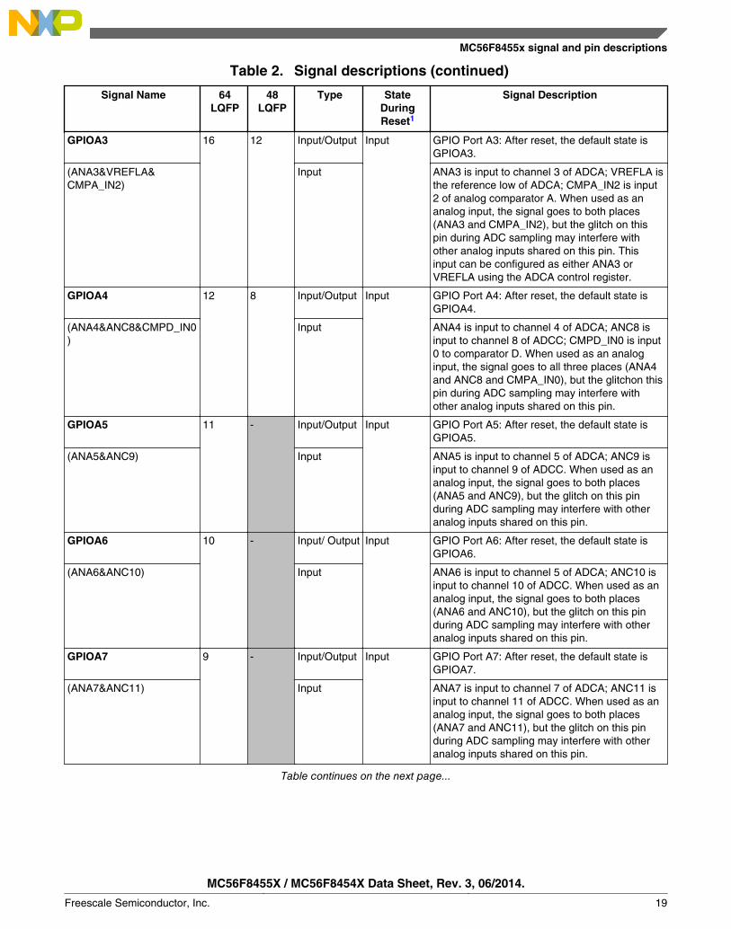
Table 2. Signal descriptions (continued)
Signal Name 64LQFP
48LQFP
Type StateDuringReset1
Signal Description
GPIOA3 16 12 Input/Output Input GPIO Port A3: After reset, the default state isGPIOA3.
(ANA3&VREFLA&CMPA_IN2)
Input ANA3 is input to channel 3 of ADCA; VREFLA isthe reference low of ADCA; CMPA_IN2 is input2 of analog comparator A. When used as ananalog input, the signal goes to both places(ANA3 and CMPA_IN2), but the glitch on thispin during ADC sampling may interfere withother analog inputs shared on this pin. Thisinput can be configured as either ANA3 orVREFLA using the ADCA control register.
GPIOA4 12 8 Input/Output Input GPIO Port A4: After reset, the default state isGPIOA4.
(ANA4&ANC8&CMPD_IN0)
Input ANA4 is input to channel 4 of ADCA; ANC8 isinput to channel 8 of ADCC; CMPD_IN0 is input0 to comparator D. When used as an analoginput, the signal goes to all three places (ANA4and ANC8 and CMPA_IN0), but the glitchon thispin during ADC sampling may interfere withother analog inputs shared on this pin.
GPIOA5 11 - Input/Output Input GPIO Port A5: After reset, the default state isGPIOA5.
(ANA5&ANC9) Input ANA5 is input to channel 5 of ADCA; ANC9 isinput to channel 9 of ADCC. When used as ananalog input, the signal goes to both places(ANA5 and ANC9), but the glitch on this pinduring ADC sampling may interfere with otheranalog inputs shared on this pin.
GPIOA6 10 - Input/ Output Input GPIO Port A6: After reset, the default state isGPIOA6.
(ANA6&ANC10) Input ANA6 is input to channel 5 of ADCA; ANC10 isinput to channel 10 of ADCC. When used as ananalog input, the signal goes to both places(ANA6 and ANC10), but the glitch on this pinduring ADC sampling may interfere with otheranalog inputs shared on this pin.
GPIOA7 9 - Input/Output Input GPIO Port A7: After reset, the default state isGPIOA7.
(ANA7&ANC11) Input ANA7 is input to channel 7 of ADCA; ANC11 isinput to channel 11 of ADCC. When used as ananalog input, the signal goes to both places(ANA7 and ANC11), but the glitch on this pinduring ADC sampling may interfere with otheranalog inputs shared on this pin.
Table continues on the next page...
MC56F8455x signal and pin descriptions
MC56F8455X / MC56F8454X Data Sheet, Rev. 3, 06/2014.
Freescale Semiconductor, Inc. 19
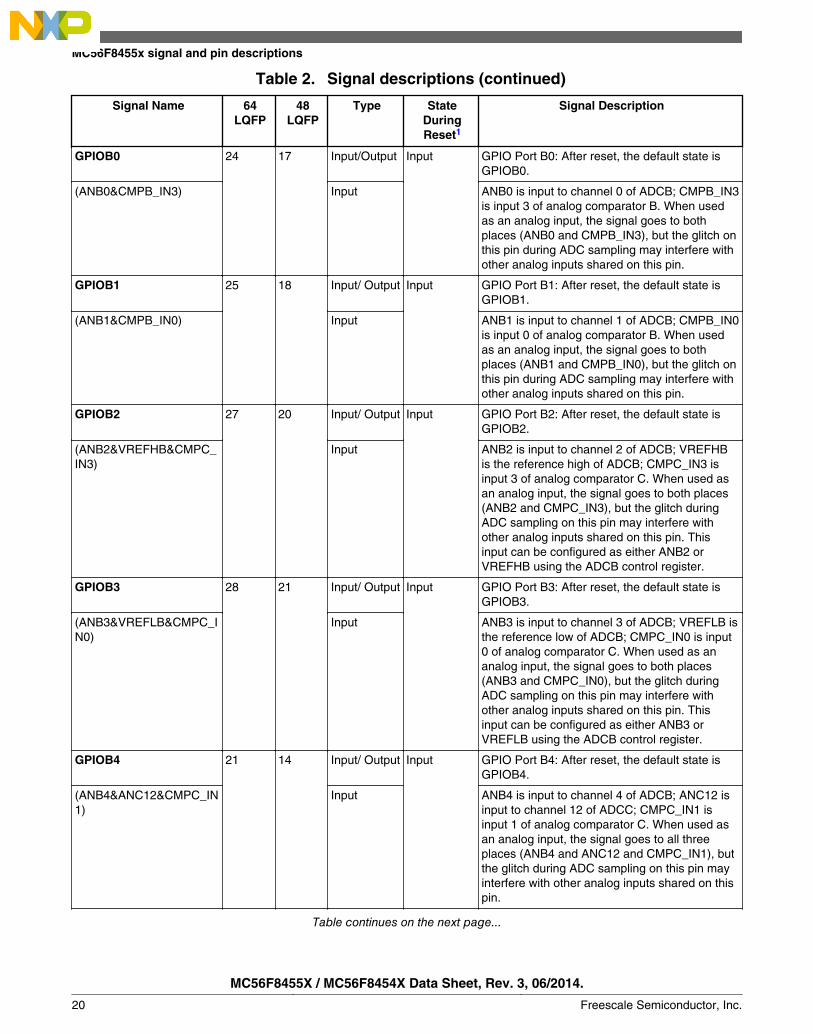
Table 2. Signal descriptions (continued)
Signal Name 64LQFP
48LQFP
Type StateDuringReset1
Signal Description
GPIOB0 24 17 Input/Output Input GPIO Port B0: After reset, the default state isGPIOB0.
(ANB0&CMPB_IN3) Input ANB0 is input to channel 0 of ADCB; CMPB_IN3is input 3 of analog comparator B. When usedas an analog input, the signal goes to bothplaces (ANB0 and CMPB_IN3), but the glitch onthis pin during ADC sampling may interfere withother analog inputs shared on this pin.
GPIOB1 25 18 Input/ Output Input GPIO Port B1: After reset, the default state isGPIOB1.
(ANB1&CMPB_IN0) Input ANB1 is input to channel 1 of ADCB; CMPB_IN0is input 0 of analog comparator B. When usedas an analog input, the signal goes to bothplaces (ANB1 and CMPB_IN0), but the glitch onthis pin during ADC sampling may interfere withother analog inputs shared on this pin.
GPIOB2 27 20 Input/ Output Input GPIO Port B2: After reset, the default state isGPIOB2.
(ANB2&VREFHB&CMPC_IN3)
Input ANB2 is input to channel 2 of ADCB; VREFHBis the reference high of ADCB; CMPC_IN3 isinput 3 of analog comparator C. When used asan analog input, the signal goes to both places(ANB2 and CMPC_IN3), but the glitch duringADC sampling on this pin may interfere withother analog inputs shared on this pin. Thisinput can be configured as either ANB2 orVREFHB using the ADCB control register.
GPIOB3 28 21 Input/ Output Input GPIO Port B3: After reset, the default state isGPIOB3.
(ANB3&VREFLB&CMPC_IN0)
Input ANB3 is input to channel 3 of ADCB; VREFLB isthe reference low of ADCB; CMPC_IN0 is input0 of analog comparator C. When used as ananalog input, the signal goes to both places(ANB3 and CMPC_IN0), but the glitch duringADC sampling on this pin may interfere withother analog inputs shared on this pin. Thisinput can be configured as either ANB3 orVREFLB using the ADCB control register.
GPIOB4 21 14 Input/ Output Input GPIO Port B4: After reset, the default state isGPIOB4.
(ANB4&ANC12&CMPC_IN1)
Input ANB4 is input to channel 4 of ADCB; ANC12 isinput to channel 12 of ADCC; CMPC_IN1 isinput 1 of analog comparator C. When used asan analog input, the signal goes to all threeplaces (ANB4 and ANC12 and CMPC_IN1), butthe glitch during ADC sampling on this pin mayinterfere with other analog inputs shared on thispin.
Table continues on the next page...
MC56F8455x signal and pin descriptions
MC56F8455X / MC56F8454X Data Sheet, Rev. 3, 06/2014.
20 Freescale Semiconductor, Inc.
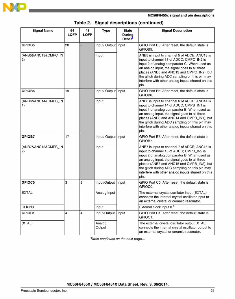
Table 2. Signal descriptions (continued)
Signal Name 64LQFP
48LQFP
Type StateDuringReset1
Signal Description
GPIOB5 20 - Input/ Output Input GPIO Port B5: After reset, the default state isGPIOB5.
(ANB5&ANC13&CMPC_IN2)
Input ANB5 is input to channel 5 of ADCB; ANC13 isinput to channel 13 of ADCC; CMPC_IN2 isinput 2 of analog comparator C. When used asan analog input, the signal goes to all threeplaces (ANB5 and ANC13 and CMPC_IN2), butthe glitch during ADC sampling on this pin mayinterfere with other analog inputs shared on thispin.
GPIOB6 19 - Input/ Output Input GPIO Port B6: After reset, the default state isGPIOB6.
(ANB6&ANC14&CMPB_IN1)
Input ANB6 is input to channel 6 of ADCB; ANC14 isinput to channel 14 of ADCC; CMPB_IN1 isinput 1 of analog comparator B. When used asan analog input, the signal goes to all threeplaces (ANB6 and ANC14 and CMPB_IN1), butthe glitch during ADC sampling on this pin mayinterfere with other analog inputs shared on thispin.
GPIOB7 17 - Input/ Output Input GPIO Port B7: After reset, the default state isGPIOB7.
(ANB7&ANC15&CMPB_IN2)
Input ANB7 is input to channel 7 of ADCB; ANC15 isinput to channel 15 of ADCC; CMPB_IN2 isinput 2 of analog comparator B. When used asan analog input, the signal goes to all threeplaces (ANB7 and ANC15 and CMPB_IN2), butthe glitch during ADC sampling on this pin mayinterfere with other analog inputs shared on thispin.
GPIOC0 3 3 Input/Output Input GPIO Port C0: After reset, the default state isGPIOC0.
EXTAL Analog Input The external crystal oscillator input (EXTAL)connects the internal crystal oscillator input toan external crystal or ceramic resonator.
CLKIN0 Input External clock input 0.2
GPIOC1 4 4 Input/Output Input GPIO Port C1: After reset, the default state isGPIOC1.
(XTAL) AnalogOutput
The external crystal oscillator output (XTAL)connects the internal crystal oscillator output toan external crystal or ceramic resonator.
Table continues on the next page...
MC56F8455x signal and pin descriptions
MC56F8455X / MC56F8454X Data Sheet, Rev. 3, 06/2014.
Freescale Semiconductor, Inc. 21
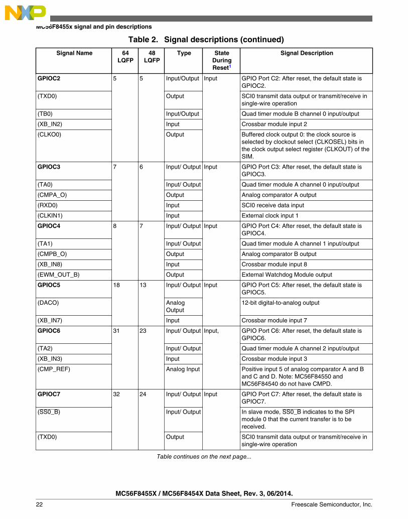
Table 2. Signal descriptions (continued)
Signal Name 64LQFP
48LQFP
Type StateDuringReset1
Signal Description
GPIOC2 5 5 Input/Output Input GPIO Port C2: After reset, the default state isGPIOC2.
(TXD0) Output SCI0 transmit data output or transmit/receive insingle-wire operation
(TB0) Input/Output Quad timer module B channel 0 input/output
(XB_IN2) Input Crossbar module input 2
(CLKO0) Output Buffered clock output 0: the clock source isselected by clockout select (CLKOSEL) bits inthe clock output select register (CLKOUT) of theSIM.
GPIOC3 7 6 Input/ Output Input GPIO Port C3: After reset, the default state isGPIOC3.
(TA0) Input/ Output Quad timer module A channel 0 input/output
(CMPA_O) Output Analog comparator A output
(RXD0) Input SCI0 receive data input
(CLKIN1) Input External clock input 1
GPIOC4 8 7 Input/ Output Input GPIO Port C4: After reset, the default state isGPIOC4.
(TA1) Input/ Output Quad timer module A channel 1 input/output
(CMPB_O) Output Analog comparator B output
(XB_IN8) Input Crossbar module input 8
(EWM_OUT_B) Output External Watchdog Module output
GPIOC5 18 13 Input/ Output Input GPIO Port C5: After reset, the default state isGPIOC5.
(DACO) AnalogOutput
12-bit digital-to-analog output
(XB_IN7) Input Crossbar module input 7
GPIOC6 31 23 Input/ Output Input, GPIO Port C6: After reset, the default state isGPIOC6.
(TA2) Input/ Output Quad timer module A channel 2 input/output
(XB_IN3) Input Crossbar module input 3
(CMP_REF) Analog Input Positive input 5 of analog comparator A and Band C and D. Note: MC56F84550 andMC56F84540 do not have CMPD.
GPIOC7 32 24 Input/ Output Input GPIO Port C7: After reset, the default state isGPIOC7.
(SS0_B) Input/ Output In slave mode, SS0_B indicates to the SPImodule 0 that the current transfer is to bereceived.
(TXD0) Output SCI0 transmit data output or transmit/receive insingle-wire operation
Table continues on the next page...
MC56F8455x signal and pin descriptions
MC56F8455X / MC56F8454X Data Sheet, Rev. 3, 06/2014.
22 Freescale Semiconductor, Inc.
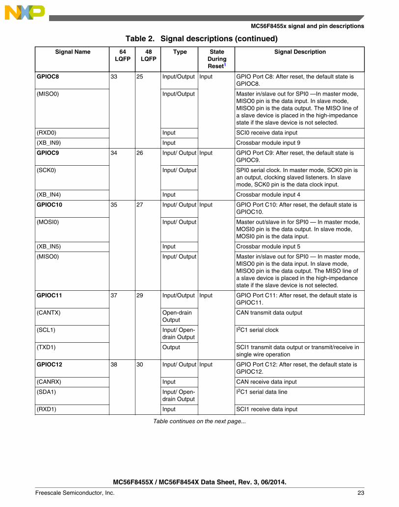
Table 2. Signal descriptions (continued)
Signal Name 64LQFP
48LQFP
Type StateDuringReset1
Signal Description
GPIOC8 33 25 Input/Output Input GPIO Port C8: After reset, the default state isGPIOC8.
(MISO0) Input/Output Master in/slave out for SPI0 —In master mode,MISO0 pin is the data input. In slave mode,MISO0 pin is the data output. The MISO line ofa slave device is placed in the high-impedancestate if the slave device is not selected.
(RXD0) Input SCI0 receive data input
(XB_IN9) Input Crossbar module input 9
GPIOC9 34 26 Input/ Output Input GPIO Port C9: After reset, the default state isGPIOC9.
(SCK0) Input/ Output SPI0 serial clock. In master mode, SCK0 pin isan output, clocking slaved listeners. In slavemode, SCK0 pin is the data clock input.
(XB_IN4) Input Crossbar module input 4
GPIOC10 35 27 Input/ Output Input GPIO Port C10: After reset, the default state isGPIOC10.
(MOSI0) Input/ Output Master out/slave in for SPI0 — In master mode,MOSI0 pin is the data output. In slave mode,MOSI0 pin is the data input.
(XB_IN5) Input Crossbar module input 5
(MISO0) Input/ Output Master in/slave out for SPI0 — In master mode,MISO0 pin is the data input. In slave mode,MISO0 pin is the data output. The MISO line ofa slave device is placed in the high-impedancestate if the slave device is not selected.
GPIOC11 37 29 Input/Output Input GPIO Port C11: After reset, the default state isGPIOC11.
(CANTX) Open-drainOutput
CAN transmit data output
(SCL1) Input/ Open-drain Output
I2C1 serial clock
(TXD1) Output SCI1 transmit data output or transmit/receive insingle wire operation
GPIOC12 38 30 Input/ Output Input GPIO Port C12: After reset, the default state isGPIOC12.
(CANRX) Input CAN receive data input
(SDA1) Input/ Open-drain Output
I2C1 serial data line
(RXD1) Input SCI1 receive data input
Table continues on the next page...
MC56F8455x signal and pin descriptions
MC56F8455X / MC56F8454X Data Sheet, Rev. 3, 06/2014.
Freescale Semiconductor, Inc. 23
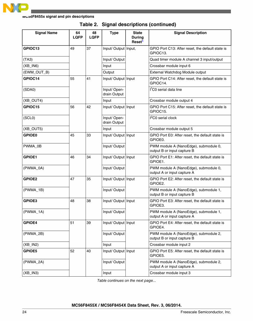
Table 2. Signal descriptions (continued)
Signal Name 64LQFP
48LQFP
Type StateDuringReset1
Signal Description
GPIOC13 49 37 Input/ Output Input, GPIO Port C13: After reset, the default state isGPIOC13.
(TA3) Input/ Output Quad timer module A channel 3 input/output
(XB_IN6) Input Crossbar module input 6
(EWM_OUT_B) Output External Watchdog Module output
GPIOC14 55 41 Input/ Output Input GPIO Port C14: After reset, the default state isGPIOC14.
(SDA0) Input/ Open-drain Output
I2C0 serial data line
(XB_OUT4) Input Crossbar module output 4
GPIOC15 56 42 Input/ Output Input GPIO Port C15: After reset, the default state isGPIOC15.
(SCL0) Input/ Open-drain Output
I2C0 serial clock
(XB_OUT5) Input Crossbar module output 5
GPIOE0 45 33 Input/ Output Input GPIO Port E0: After reset, the default state isGPIOE0.
PWMA_0B Input/ Output PWM module A (NanoEdge), submodule 0,output B or input capture B
GPIOE1 46 34 Input/ Output Input GPIO Port E1: After reset, the default state isGPIOE1.
(PWMA_0A) Input/ Output PWM module A (NanoEdge), submodule 0,output A or input capture A
GPIOE2 47 35 Input/ Output Input GPIO Port E2: After reset, the default state isGPIOE2.
(PWMA_1B) Input/ Output PWM module A (NanoEdge), submodule 1,output B or input capture B
GPIOE3 48 38 Input/ Output Input GPIO Port E3: After reset, the default state isGPIOE3.
(PWMA_1A) Input/ Output PWM module A (NanoEdge), submodule 1,output A or input capture A
GPIOE4 51 39 Input/ Output Input GPIO Port E4: After reset, the default state isGPIOE4.
(PWMA_2B) Input/ Output PWM module A (NanoEdge), submodule 2,output B or input capture B
(XB_IN2) Input Crossbar module input 2
GPIOE5 52 40 Input/ Output Input GPIO Port E5: After reset, the default state isGPIOE5.
(PWMA_2A) Input/ Output PWM module A (NanoEdge), submodule 2,output A or input capture A
(XB_IN3) Input Crossbar module input 3
Table continues on the next page...
MC56F8455x signal and pin descriptions
MC56F8455X / MC56F8454X Data Sheet, Rev. 3, 06/2014.
24 Freescale Semiconductor, Inc.
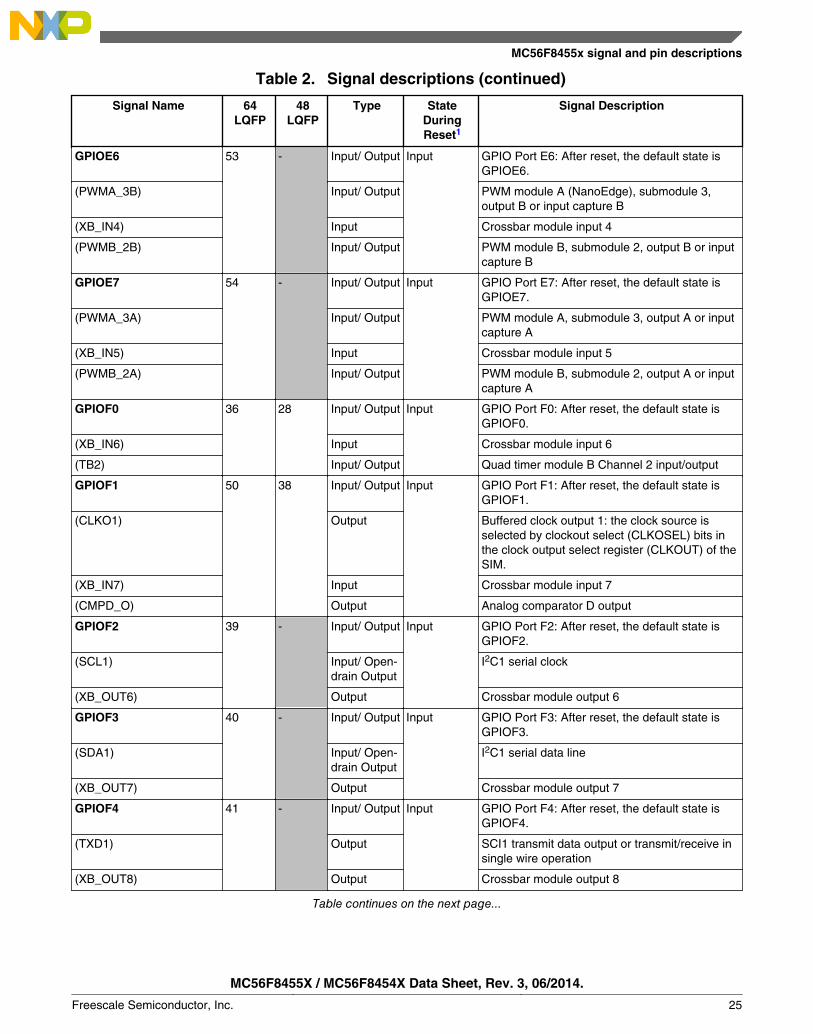
Table 2. Signal descriptions (continued)
Signal Name 64LQFP
48LQFP
Type StateDuringReset1
Signal Description
GPIOE6 53 - Input/ Output Input GPIO Port E6: After reset, the default state isGPIOE6.
(PWMA_3B) Input/ Output PWM module A (NanoEdge), submodule 3,output B or input capture B
(XB_IN4) Input Crossbar module input 4
(PWMB_2B) Input/ Output PWM module B, submodule 2, output B or inputcapture B
GPIOE7 54 - Input/ Output Input GPIO Port E7: After reset, the default state isGPIOE7.
(PWMA_3A) Input/ Output PWM module A, submodule 3, output A or inputcapture A
(XB_IN5) Input Crossbar module input 5
(PWMB_2A) Input/ Output PWM module B, submodule 2, output A or inputcapture A
GPIOF0 36 28 Input/ Output Input GPIO Port F0: After reset, the default state isGPIOF0.
(XB_IN6) Input Crossbar module input 6
(TB2) Input/ Output Quad timer module B Channel 2 input/output
GPIOF1 50 38 Input/ Output Input GPIO Port F1: After reset, the default state isGPIOF1.
(CLKO1) Output Buffered clock output 1: the clock source isselected by clockout select (CLKOSEL) bits inthe clock output select register (CLKOUT) of theSIM.
(XB_IN7) Input Crossbar module input 7
(CMPD_O) Output Analog comparator D output
GPIOF2 39 - Input/ Output Input GPIO Port F2: After reset, the default state isGPIOF2.
(SCL1) Input/ Open-drain Output
I2C1 serial clock
(XB_OUT6) Output Crossbar module output 6
GPIOF3 40 - Input/ Output Input GPIO Port F3: After reset, the default state isGPIOF3.
(SDA1) Input/ Open-drain Output
I2C1 serial data line
(XB_OUT7) Output Crossbar module output 7
GPIOF4 41 - Input/ Output Input GPIO Port F4: After reset, the default state isGPIOF4.
(TXD1) Output SCI1 transmit data output or transmit/receive insingle wire operation
(XB_OUT8) Output Crossbar module output 8
Table continues on the next page...
MC56F8455x signal and pin descriptions
MC56F8455X / MC56F8454X Data Sheet, Rev. 3, 06/2014.
Freescale Semiconductor, Inc. 25
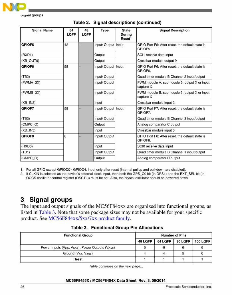
Table 2. Signal descriptions (continued)
Signal Name 64LQFP
48LQFP
Type StateDuringReset1
Signal Description
GPIOF5 42 - Input/ Output Input GPIO Port F5: After reset, the default state isGPIOF5.
(RXD1) Output SCI1 receive data input
(XB_OUT9) Output Crossbar module output 9
GPIOF6 58 - Input/ Output Input GPIO Port F6: After reset, the default state isGPIOF6.
(TB2) Input/ Output Quad timer module B Channel 2 input/output
(PWMA_3X) Input/ Output PWM module A, submodule 3, output X or inputcapture X
(PWMB_3X) Input/ Output PWM module B, submodule 3, output X or inputcapture X
(XB_IN2) Input Crossbar module input 2
GPIOF7 59 - Input/ Output Input GPIO Port F7: After reset, the default state isGPIOF7.
(TB3) Input/ Output Quad timer module B Channel 3 input/output
(CMPC_O) Output Analog comparator C output
(XB_IN3) Input Crossbar module input 3
GPIOF8 6 - Input/ Output GPIO Port F8: After reset, the default state isGPIOF8.
(RXD0) Input SCI0 receive data input
(TB1) Input/ Output Quad timer module B Channel 1 input/output
(CMPD_O) Output Analog comparator D output
1. For all GPIO except GPIOD0 - GPIOD4, input only after reset (internal pullup and pull-down are disabled).2. If CLKIN is selected as the device’s external clock input, then both the GPS_C0 bit (in GPS1) and the EXT_SEL bit (in
OCCS oscillator control register (OSCTL)) must be set. Also, the crystal oscillator should be powered down.
3 Signal groupsThe input and output signals of the MC56F84xxx are organized into functional groups, aslisted in Table 3. Note that some package sizes may not be available for your specificproduct. See MC56F844xx/5xx/7xx product family.
Table 3. Functional Group Pin Allocations
Functional Group Number of Pins
48 LQFP 64 LQFP 80 LQFP 100 LQFP
Power Inputs (VDD, VDDA), Power Outputs (VCAP) 5 6 6 6
Ground (VSS, VSSA) 4 4 5 6
Reset 1 1 1 1
Table continues on the next page...
Signal groups
MC56F8455X / MC56F8454X Data Sheet, Rev. 3, 06/2014.
26 Freescale Semiconductor, Inc.
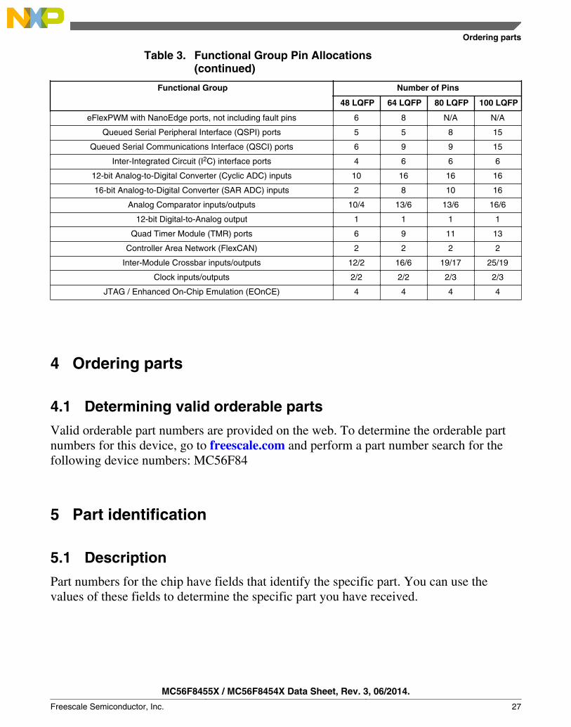
Table 3. Functional Group Pin Allocations(continued)
Functional Group Number of Pins
48 LQFP 64 LQFP 80 LQFP 100 LQFP
eFlexPWM with NanoEdge ports, not including fault pins 6 8 N/A N/A
Queued Serial Peripheral Interface (QSPI) ports 5 5 8 15
Queued Serial Communications Interface (QSCI) ports 6 9 9 15
Inter-Integrated Circuit (I2C) interface ports 4 6 6 6
12-bit Analog-to-Digital Converter (Cyclic ADC) inputs 10 16 16 16
16-bit Analog-to-Digital Converter (SAR ADC) inputs 2 8 10 16
Analog Comparator inputs/outputs 10/4 13/6 13/6 16/6
12-bit Digital-to-Analog output 1 1 1 1
Quad Timer Module (TMR) ports 6 9 11 13
Controller Area Network (FlexCAN) 2 2 2 2
Inter-Module Crossbar inputs/outputs 12/2 16/6 19/17 25/19
Clock inputs/outputs 2/2 2/2 2/3 2/3
JTAG / Enhanced On-Chip Emulation (EOnCE) 4 4 4 4
4 Ordering parts
4.1 Determining valid orderable parts
Valid orderable part numbers are provided on the web. To determine the orderable partnumbers for this device, go to freescale.com and perform a part number search for thefollowing device numbers: MC56F84
5 Part identification
5.1 Description
Part numbers for the chip have fields that identify the specific part. You can use thevalues of these fields to determine the specific part you have received.
Ordering parts
MC56F8455X / MC56F8454X Data Sheet, Rev. 3, 06/2014.
Freescale Semiconductor, Inc. 27
5.2 Format
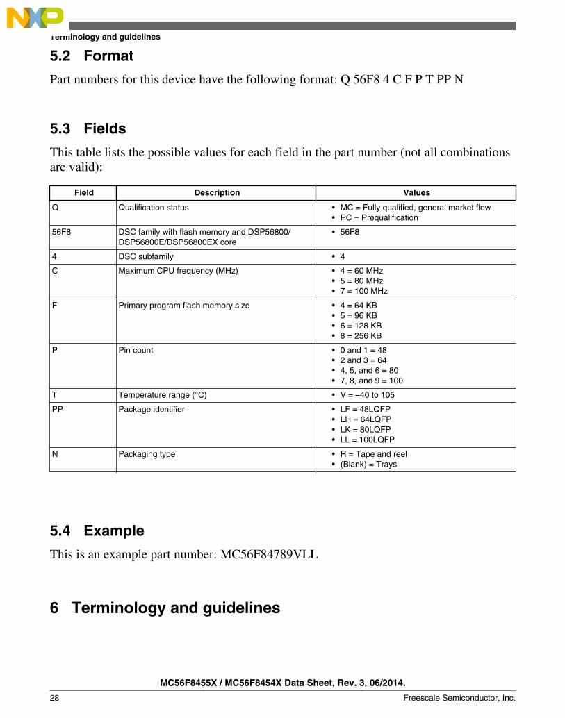
Part numbers for this device have the following format: Q 56F8 4 C F P T PP N
5.3 Fields
This table lists the possible values for each field in the part number (not all combinationsare valid):
Field Description Values
Q Qualification status • MC = Fully qualified, general market flow• PC = Prequalification
56F8 DSC family with flash memory and DSP56800/DSP56800E/DSP56800EX core
• 56F8
4 DSC subfamily • 4
C Maximum CPU frequency (MHz) • 4 = 60 MHz• 5 = 80 MHz• 7 = 100 MHz
F Primary program flash memory size • 4 = 64 KB• 5 = 96 KB• 6 = 128 KB• 8 = 256 KB
P Pin count • 0 and 1 = 48• 2 and 3 = 64• 4, 5, and 6 = 80• 7, 8, and 9 = 100
T Temperature range (°C) • V = –40 to 105
PP Package identifier • LF = 48LQFP• LH = 64LQFP• LK = 80LQFP• LL = 100LQFP
N Packaging type • R = Tape and reel• (Blank) = Trays
5.4 Example
This is an example part number: MC56F84789VLL
6 Terminology and guidelines
Terminology and guidelines
MC56F8455X / MC56F8454X Data Sheet, Rev. 3, 06/2014.
28 Freescale Semiconductor, Inc.
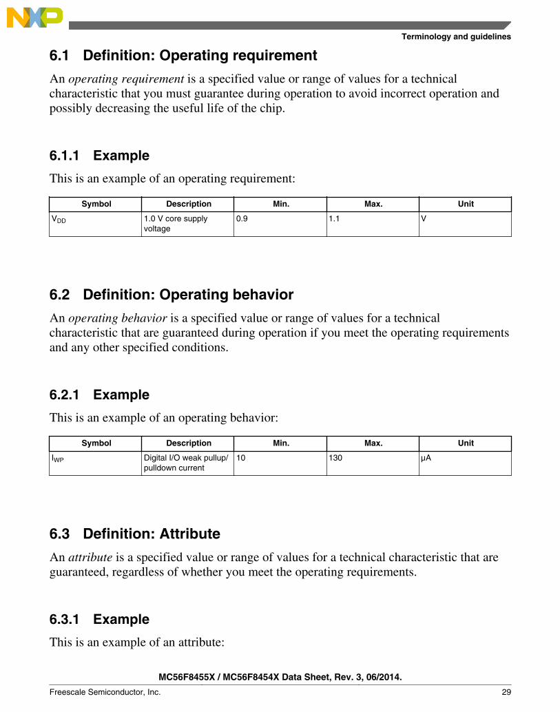
6.1 Definition: Operating requirement
An operating requirement is a specified value or range of values for a technicalcharacteristic that you must guarantee during operation to avoid incorrect operation andpossibly decreasing the useful life of the chip.
6.1.1 Example
This is an example of an operating requirement:
Symbol Description Min. Max. Unit
VDD 1.0 V core supplyvoltage
0.9 1.1 V
6.2 Definition: Operating behavior
An operating behavior is a specified value or range of values for a technicalcharacteristic that are guaranteed during operation if you meet the operating requirementsand any other specified conditions.
6.2.1 Example
This is an example of an operating behavior:
Symbol Description Min. Max. Unit
IWP Digital I/O weak pullup/pulldown current
10 130 µA
6.3 Definition: Attribute
An attribute is a specified value or range of values for a technical characteristic that areguaranteed, regardless of whether you meet the operating requirements.
6.3.1 Example
This is an example of an attribute:
Terminology and guidelines
MC56F8455X / MC56F8454X Data Sheet, Rev. 3, 06/2014.
Freescale Semiconductor, Inc. 29
Symbol Description Min. Max. Unit
CIN_D Input capacitance:digital pins
— 7 pF
6.4 Definition: Rating
A rating is a minimum or maximum value of a technical characteristic that, if exceeded,may cause permanent chip failure:
• Operating ratings apply during operation of the chip.• Handling ratings apply when the chip is not powered.
6.4.1 Example
This is an example of an operating rating:
Symbol Description Min. Max. Unit
VDD 1.0 V core supplyvoltage
–0.3 1.2 V
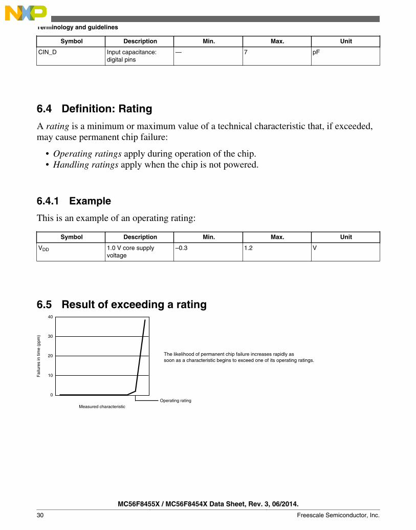
6.5 Result of exceeding a rating40
30
20
10
0
Measured characteristicOperating rating
Fai
lure
s in
tim
e (p
pm)
The likelihood of permanent chip failure increases rapidly as soon as a characteristic begins to exceed one of its operating ratings.
Terminology and guidelines
MC56F8455X / MC56F8454X Data Sheet, Rev. 3, 06/2014.
30 Freescale Semiconductor, Inc.
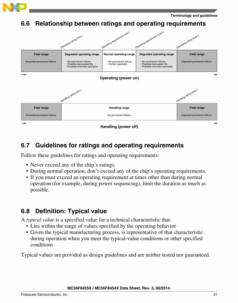
6.6 Relationship between ratings and operating requirements
–∞
- No permanent failure- Correct operation
Normal operating rangeFatal range
Expected permanent failure
Fatal range
Expected permanent failure
∞
Operating rating (m
ax.)
Operating requirement (m
ax.)
Operating requirement (m
in.)
Operating rating (m
in.)
Operating (power on)
Degraded operating range Degraded operating range
–∞
No permanent failure
Handling rangeFatal range
Expected permanent failure
Fatal range
Expected permanent failure
∞
Handling rating (m
ax.)
Handling rating (m
in.)
Handling (power off)
- No permanent failure- Possible decreased life- Possible incorrect operation
- No permanent failure- Possible decreased life- Possible incorrect operation
6.7 Guidelines for ratings and operating requirements
Follow these guidelines for ratings and operating requirements:
• Never exceed any of the chip’s ratings.• During normal operation, don’t exceed any of the chip’s operating requirements.• If you must exceed an operating requirement at times other than during normal
operation (for example, during power sequencing), limit the duration as much aspossible.
6.8 Definition: Typical valueA typical value is a specified value for a technical characteristic that:
• Lies within the range of values specified by the operating behavior• Given the typical manufacturing process, is representative of that characteristic
during operation when you meet the typical-value conditions or other specifiedconditions
Typical values are provided as design guidelines and are neither tested nor guaranteed.
Terminology and guidelines
MC56F8455X / MC56F8454X Data Sheet, Rev. 3, 06/2014.
Freescale Semiconductor, Inc. 31
6.8.1 Example 1
This is an example of an operating behavior that includes a typical value:
Symbol Description Min. Typ. Max. Unit
IWP Digital I/O weakpullup/pulldowncurrent
10 70 130 µA
6.8.2 Example 2
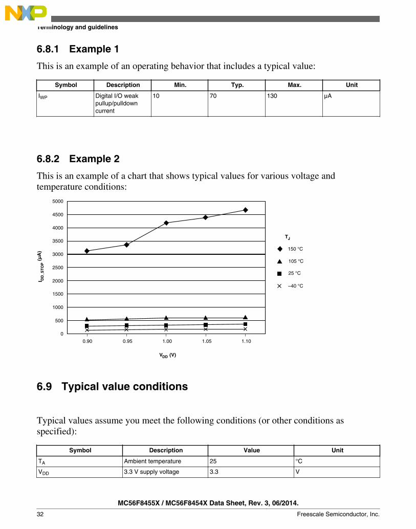
This is an example of a chart that shows typical values for various voltage andtemperature conditions:
0.90 0.95 1.00 1.05 1.10
0
500
1000
1500
2000
2500
3000
3500
4000
4500
5000
150 °C
105 °C
25 °C
–40 °C
VDD (V)
I(μ
A)
DD
_ST
OP
TJ
6.9 Typical value conditions
Typical values assume you meet the following conditions (or other conditions asspecified):
Symbol Description Value Unit
TA Ambient temperature 25 °C
VDD 3.3 V supply voltage 3.3 V
Terminology and guidelines
MC56F8455X / MC56F8454X Data Sheet, Rev. 3, 06/2014.
32 Freescale Semiconductor, Inc.
7 Ratings
7.1 Thermal handling ratings
Symbol Description Min. Max. Unit Notes
TSTG Storage temperature –55 150 °C 1
TSDR Solder temperature, lead-free — 260 °C 2
1. Determined according to JEDEC Standard JESD22-A103, High Temperature Storage Life.2. Determined according to IPC/JEDEC Standard J-STD-020, Moisture/Reflow Sensitivity Classification for Nonhermetic
Solid State Surface Mount Devices.
7.2 Moisture handling ratings
Symbol Description Min. Max. Unit Notes
MSL Moisture sensitivity level — 3 — 1
1. Determined according to IPC/JEDEC Standard J-STD-020, Moisture/Reflow Sensitivity Classification for NonhermeticSolid State Surface Mount Devices.
7.3 ESD handling ratings
Although damage from electrostatic discharge (ESD) is much less common on thesedevices than on early CMOS circuits, use normal handling precautions to avoid exposureto static discharge. Qualification tests are performed to ensure that these devices canwithstand exposure to reasonable levels of static without suffering any permanentdamage.
All ESD testing is in conformity with AEC-Q100 Stress Test Qualification. During thedevice qualification ESD stresses were performed for the human body model (HBM), themachine model (MM), and the charge device model (CDM).
All latch-up testing is in conformity with AEC-Q100 Stress Test Qualification.
A device is defined as a failure if after exposure to ESD pulses, the device no longermeets the device specification. Complete DC parametric and functional testing isperformed as per the applicable device specification at room temperature followed by hottemperature, unless specified otherwise in the device specification.
Ratings
MC56F8455X / MC56F8454X Data Sheet, Rev. 3, 06/2014.
Freescale Semiconductor, Inc. 33
Table 4. ESD/Latch-up Protection
Characteristic1 Min Max Unit
ESD for Human Body Model (HBM) –2000 +2000 V
ESD for Machine Model (MM) –200 +200 V
ESD for Charge Device Model (CDM) –500 +500 V
Latch-up current at TA= 85°C (ILAT) –100 +100 mA
1. Parameter is achieved by design characterization on a small sample size from typical devices under typical conditionsunless otherwise noted.
7.4 Voltage and current operating ratings
Absolute maximum ratings are stress ratings only, and functional operation at themaxima is not guaranteed. Stress beyond the limits specified in Table 5 may affect devicereliability or cause permanent damage to the device.
Table 5. Absolute Maximum Ratings (VSS = 0 V, VSSA = 0 V)
Characteristic Symbol Notes1 Min Max Unit
Supply Voltage Range VDD -0.3 4.0 V
Analog Supply Voltage Range VDDA -0.3 4.0 V
ADC High Voltage Reference VREFHx -0.3 4.0 V
Voltage difference VDD to VDDA ΔVDD -0.3 0.3 V
Voltage difference VSS to VSSA ΔVSS -0.3 0.3 V
Digital Input Voltage Range VIN Pin Group 1 -0.3 5.5 V
RESET Input Voltage Range VIN_RESET Pin Group 2 -0.3 4.0 V
Oscillator Input Voltage Range VOSC Pin Group 4 -0.4 4.0 V
Analog Input Voltage Range VINA Pin Group 3 -0.3 4.0 V
Input clamp current, per pin (VIN < VSS - 0.3 V)2, 3 VIC — -5.0 mA
Output clamp current, per pin4 VOC — ±20.0 mA
Contiguous pin DC injection current—regional limit sumof 16 contiguous pins
IICont -25 25 mA
Output Voltage Range (normal push-pull mode) VOUT Pin Group 1, 2 -0.3 4.0 V
Output Voltage Range (open drain mode) VOUTOD Pin Group 1 -0.3 5.5 V
RESET Output Voltage Range VOUTOD_RE
SET
Pin Group 2 -0.3 4.0 V
DAC Output Voltage Range VOUT_DAC Pin Group 5 -0.3 4.0 V
Ambient Temperature Industrial TA -40 105 °C
Junction Temperature Tj -40 125 °C
Storage Temperature Range (Extended Industrial) TSTG -55 150 °C
1. Default Mode
• Pin Group 1: GPIO, TDI, TDO, TMS, TCK• Pin Group 2: RESET
Ratings
MC56F8455X / MC56F8454X Data Sheet, Rev. 3, 06/2014.
34 Freescale Semiconductor, Inc.
• Pin Group 3: ADC and Comparator Analog Inputs• Pin Group 4: XTAL, EXTAL• Pin Group 5: DAC analog output
2. Continuous clamp current3. All 5 volt tolerant digital I/O pins are internally clamped to VSS through a ESD protection diode. There is no diode
connection to VDD. If VIN greater than VDIO_MIN (= VSS–0.3 V) is observed, then there is no need to provide currentlimiting resistors at the pads. If this limit cannot be observed, then a current limiting resistor is required.
4. I/O is configured as push-pull mode.
8 General
8.1 General characteristics
The device is fabricated in high-density, low-power CMOS with 5 V–tolerant TTL-compatible digital inputs, except for the RESET pin which is 3.3V only. The term “5 V–tolerant” refers to the capability of an I/O pin, built on a 3.3 V–compatible processtechnology, to withstand a voltage up to 5.5 V without damaging the device.
5 V–tolerant I/O is desirable because many systems have a mixture of devices designedfor 3.3 V and 5 V power supplies. In such systems, a bus may carry both 3.3 V– and 5 V–compatible I/O voltage levels (a standard 3.3 V I/O is designed to receive a maximumvoltage of 3.3 V ± 10% during normal operation without causing damage). This 5 V–tolerant capability therefore offers the power savings of 3.3 V I/O levels combined withthe ability to receive 5 V levels without damage.
Absolute maximum ratings in Table 5 are stress ratings only, and functional operation atthe maximum is not guaranteed. Stress beyond these ratings may affect device reliabilityor cause permanent damage to the device.
Unless otherwise stated, all specifications within this chapter apply over the temperaturerange of -40°C to 105°C ambient temperature over the following supply ranges:VSS=VSSA=0V, VDD=VDDA=3.0V to 3.6V, CL≤50 pF, fOP=80MHz.
CAUTIONThis device contains protective circuitry to guard againstdamage due to high static voltage or electrical fields. However,normal precautions are advised to avoid application of anyvoltages higher than maximum-rated voltages to this high-impedance circuit. Reliability of operation is enhanced ifunused inputs are tied to an appropriate voltage level.
General
MC56F8455X / MC56F8454X Data Sheet, Rev. 3, 06/2014.
Freescale Semiconductor, Inc. 35
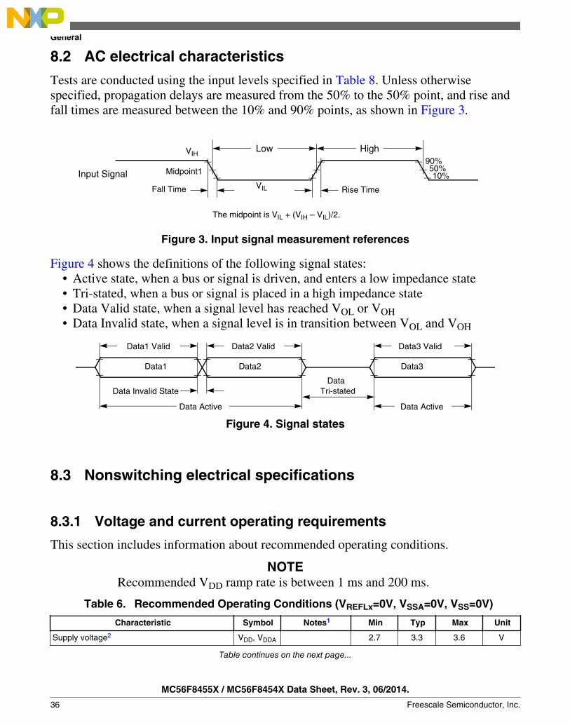
8.2 AC electrical characteristics
Tests are conducted using the input levels specified in Table 8. Unless otherwisespecified, propagation delays are measured from the 50% to the 50% point, and rise andfall times are measured between the 10% and 90% points, as shown in Figure 3.
VIH
VILFall Time
Midpoint1
Low High90%50%10%
Rise Time
The midpoint is VIL + (VIH – VIL)/2.
Input Signal
Figure 3. Input signal measurement references
Figure 4 shows the definitions of the following signal states:• Active state, when a bus or signal is driven, and enters a low impedance state• Tri-stated, when a bus or signal is placed in a high impedance state• Data Valid state, when a signal level has reached VOL or VOH• Data Invalid state, when a signal level is in transition between VOL and VOH
Data Invalid State
Data1
Data3 Valid
Data2 Data3
Data1 Valid
Data Active Data Active
Data2 Valid
DataTri-stated
Figure 4. Signal states
8.3 Nonswitching electrical specifications
8.3.1 Voltage and current operating requirements
This section includes information about recommended operating conditions.
NOTERecommended VDD ramp rate is between 1 ms and 200 ms.
Table 6. Recommended Operating Conditions (VREFLx=0V, VSSA=0V, VSS=0V)
Characteristic Symbol Notes1 Min Typ Max Unit
Supply voltage2 VDD, VDDA 2.7 3.3 3.6 V
Table continues on the next page...
General
MC56F8455X / MC56F8454X Data Sheet, Rev. 3, 06/2014.
36 Freescale Semiconductor, Inc.
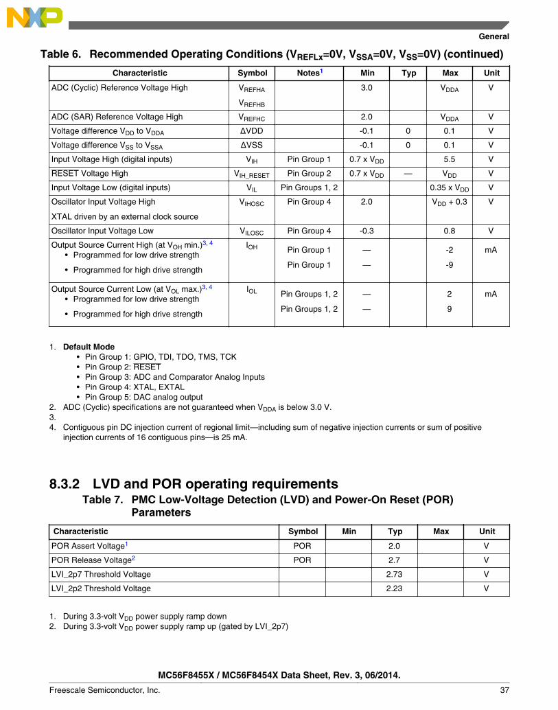
Table 6. Recommended Operating Conditions (VREFLx=0V, VSSA=0V, VSS=0V) (continued)
Characteristic Symbol Notes1 Min Typ Max Unit
ADC (Cyclic) Reference Voltage High VREFHA
VREFHB
3.0 VDDA V
ADC (SAR) Reference Voltage High VREFHC 2.0 VDDA V
Voltage difference VDD to VDDA ΔVDD -0.1 0 0.1 V
Voltage difference VSS to VSSA ΔVSS -0.1 0 0.1 V
Input Voltage High (digital inputs) VIH Pin Group 1 0.7 x VDD 5.5 V
RESET Voltage High VIH_RESET Pin Group 2 0.7 x VDD — VDD V
Input Voltage Low (digital inputs) VIL Pin Groups 1, 2 0.35 x VDD V
Oscillator Input Voltage High
XTAL driven by an external clock source
VIHOSC Pin Group 4 2.0 VDD + 0.3 V
Oscillator Input Voltage Low VILOSC Pin Group 4 -0.3 0.8 V
Output Source Current High (at VOH min.)3, 4
• Programmed for low drive strength
• Programmed for high drive strength
IOH Pin Group 1
Pin Group 1
—
—
-2
-9
mA
Output Source Current Low (at VOL max.)3, 4
• Programmed for low drive strength
• Programmed for high drive strength
IOL Pin Groups 1, 2
Pin Groups 1, 2
—
—
2
9
mA
1. Default Mode• Pin Group 1: GPIO, TDI, TDO, TMS, TCK• Pin Group 2: RESET• Pin Group 3: ADC and Comparator Analog Inputs• Pin Group 4: XTAL, EXTAL• Pin Group 5: DAC analog output
2. ADC (Cyclic) specifications are not guaranteed when VDDA is below 3.0 V.3.4. Contiguous pin DC injection current of regional limit—including sum of negative injection currents or sum of positive
injection currents of 16 contiguous pins—is 25 mA.
8.3.2 LVD and POR operating requirementsTable 7. PMC Low-Voltage Detection (LVD) and Power-On Reset (POR)
Parameters
Characteristic Symbol Min Typ Max Unit
POR Assert Voltage1 POR 2.0 V
POR Release Voltage2 POR 2.7 V
LVI_2p7 Threshold Voltage 2.73 V
LVI_2p2 Threshold Voltage 2.23 V
1. During 3.3-volt VDD power supply ramp down2. During 3.3-volt VDD power supply ramp up (gated by LVI_2p7)
General
MC56F8455X / MC56F8454X Data Sheet, Rev. 3, 06/2014.
Freescale Semiconductor, Inc. 37
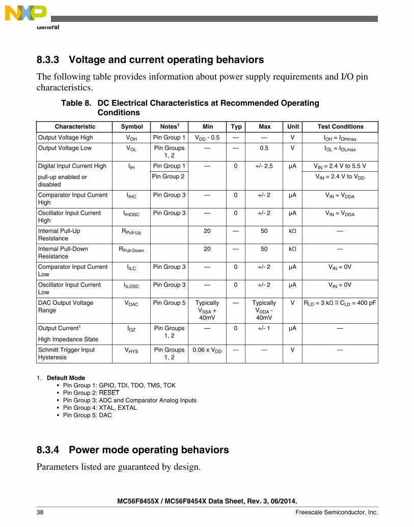
8.3.3 Voltage and current operating behaviors
The following table provides information about power supply requirements and I/O pincharacteristics.
Table 8. DC Electrical Characteristics at Recommended OperatingConditions
Characteristic Symbol Notes1 Min Typ Max Unit Test Conditions
Output Voltage High VOH Pin Group 1 VDD - 0.5 — — V IOH = IOHmax
Output Voltage Low VOL Pin Groups1, 2
— — 0.5 V IOL = IOLmax
Digital Input Current High
pull-up enabled ordisabled
IIH Pin Group 1 — 0 +/- 2.5 µA VIN = 2.4 V to 5.5 V
Pin Group 2 VIN = 2.4 V to VDD
Comparator Input CurrentHigh
IIHC Pin Group 3 — 0 +/- 2 µA VIN = VDDA
Oscillator Input CurrentHigh
IIHOSC Pin Group 3 — 0 +/- 2 µA VIN = VDDA
Internal Pull-UpResistance
RPull-Up 20 — 50 kΩ —
Internal Pull-DownResistance
RPull-Down 20 — 50 kΩ —
Comparator Input CurrentLow
IILC Pin Group 3 — 0 +/- 2 µA VIN = 0V
Oscillator Input CurrentLow
IILOSC Pin Group 3 — 0 +/- 2 µA VIN = 0V
DAC Output VoltageRange
VDAC Pin Group 5 TypicallyVSSA +40mV
— TypicallyVDDA -40mV
V RLD = 3 kΩ || CLD = 400 pF
Output Current1
High Impedance State
IOZ Pin Groups1, 2
— 0 +/- 1 µA —
Schmitt Trigger InputHysteresis
VHYS Pin Groups1, 2
0.06 x VDD — — V —
1. Default Mode• Pin Group 1: GPIO, TDI, TDO, TMS, TCK• Pin Group 2: RESET• Pin Group 3: ADC and Comparator Analog Inputs• Pin Group 4: XTAL, EXTAL• Pin Group 5: DAC
8.3.4 Power mode operating behaviors
Parameters listed are guaranteed by design.
General
MC56F8455X / MC56F8454X Data Sheet, Rev. 3, 06/2014.
38 Freescale Semiconductor, Inc.
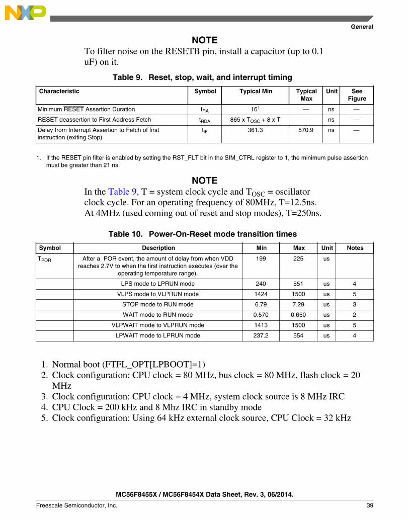
NOTETo filter noise on the RESETB pin, install a capacitor (up to 0.1uF) on it.
Table 9. Reset, stop, wait, and interrupt timing
Characteristic Symbol Typical Min TypicalMax
Unit SeeFigure
Minimum RESET Assertion Duration tRA 161 — ns —
RESET deassertion to First Address Fetch tRDA 865 x TOSC + 8 x T ns —
Delay from Interrupt Assertion to Fetch of firstinstruction (exiting Stop)
tIF 361.3 570.9 ns —
1. If the RESET pin filter is enabled by setting the RST_FLT bit in the SIM_CTRL register to 1, the minimum pulse assertionmust be greater than 21 ns.
NOTEIn the Table 9, T = system clock cycle and TOSC = oscillatorclock cycle. For an operating frequency of 80MHz, T=12.5ns.At 4MHz (used coming out of reset and stop modes), T=250ns.
Table 10. Power-On-Reset mode transition times
Symbol Description Min Max Unit Notes
TPOR After a POR event, the amount of delay from when VDDreaches 2.7V to when the first instruction executes (over the
operating temperature range).
199 225 us
LPS mode to LPRUN mode 240 551 us 4
VLPS mode to VLPRUN mode 1424 1500 us 5
STOP mode to RUN mode 6.79 7.29 us 3
WAIT mode to RUN mode 0.570 0.650 us 2
VLPWAIT mode to VLPRUN mode 1413 1500 us 5
LPWAIT mode to LPRUN mode 237.2 554 us 4
1. Normal boot (FTFL_OPT[LPBOOT]=1)2. Clock configuration: CPU clock = 80 MHz, bus clock = 80 MHz, flash clock = 20
MHz3. Clock configuration: CPU clock = 4 MHz, system clock source is 8 MHz IRC4. CPU Clock = 200 kHz and 8 Mhz IRC in standby mode5. Clock configuration: Using 64 kHz external clock source, CPU Clock = 32 kHz
General
MC56F8455X / MC56F8454X Data Sheet, Rev. 3, 06/2014.
Freescale Semiconductor, Inc. 39
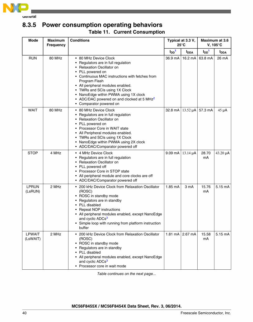
8.3.5 Power consumption operating behaviorsTable 11. Current Consumption
Mode MaximumFrequency
Conditions Typical at 3.3 V,25°C
Maximum at 3.6V, 105°C
IDD1 IDDA IDD
1 IDDA
RUN 80 MHz • 80 MHz Device Clock• Regulators are in full regulation• Relaxation Oscillator on• PLL powered on• Continuous MAC instructions with fetches from
Program Flash• All peripheral modules enabled.• TMRs and SCIs using 1X Clock• NanoEdge within PWMA using 1X clock• ADC/DAC powered on and clocked at 5 MHz2
• Comparator powered on
36.9 mA 16.2 mA 63.8 mA 26 mA
WAIT 80 MHz • 80 MHz Device Clock• Regulators are in full regulation• Relaxation Oscillator on• PLL powered on• Processor Core in WAIT state• All Peripheral modules enabled.• TMRs and SCIs using 1X Clock• NanoEdge within PWMA using 2X clock• ADC/DAC/Comparator powered off
32.8 mA 13.52 μA 57.3 mA 45 μA
STOP 4 MHz • 4 MHz Device Clock• Regulators are in full regulation• Relaxation Oscillator on• PLL powered off• Processor Core in STOP state• All peripheral module and core clocks are off• ADC/DAC/Comparator powered off
9.09 mA 13.14 μA 28.70mA
43.20 μA
LPRUN(LsRUN)
2 MHz • 200 kHz Device Clock from Relaxation Oscillator(ROSC)
• ROSC in standby mode• Regulators are in standby• PLL disabled• Repeat NOP instructions• All peripheral modules enabled, except NanoEdge
and cyclic ADCs3
• Simple loop with running from platform instructionbuffer
1.85 mA 3 mA 15.76mA
5.15 mA
LPWAIT(LsWAIT)
2 MHz • 200 kHz Device Clock from Relaxation Oscillator(ROSC)
• ROSC in standby mode• Regulators are in standby• PLL disabled• All peripheral modules enabled, except NanoEdge
and cyclic ADCs3
• Processor core in wait mode
1.81 mA 2.67 mA 15.58mA
5.15 mA
Table continues on the next page...
General
MC56F8455X / MC56F8454X Data Sheet, Rev. 3, 06/2014.
40 Freescale Semiconductor, Inc.
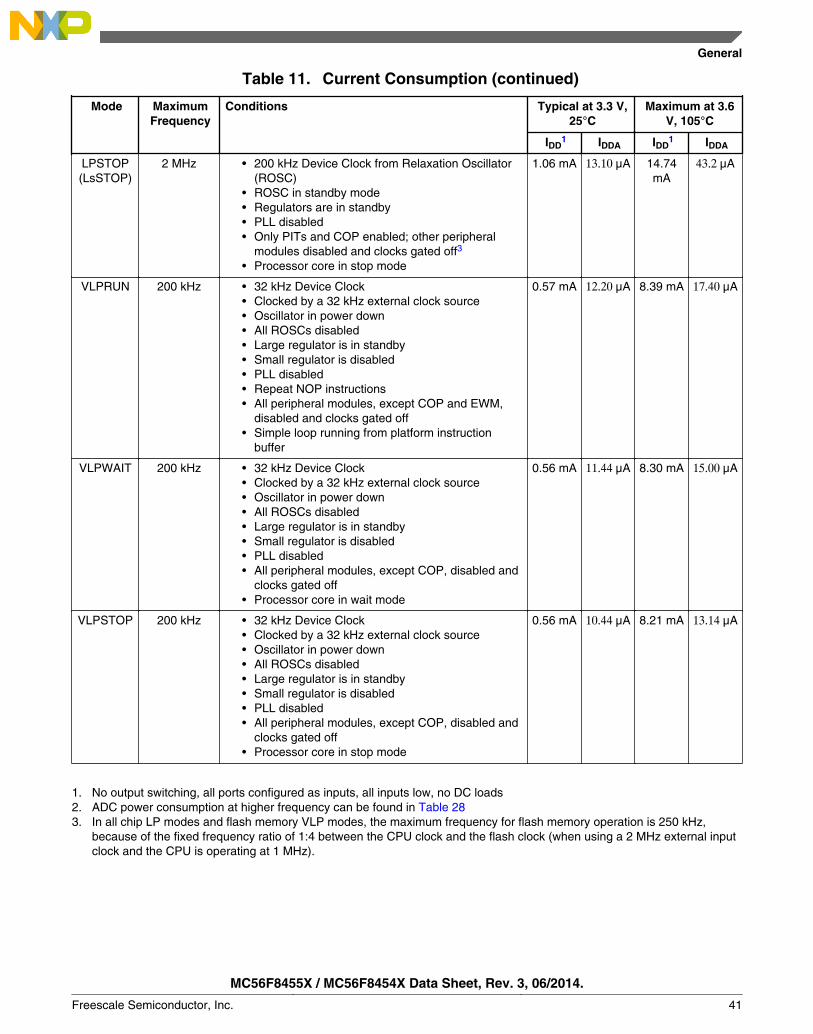
Table 11. Current Consumption (continued)
Mode MaximumFrequency
Conditions Typical at 3.3 V,25°C
Maximum at 3.6V, 105°C
IDD1 IDDA IDD
1 IDDA
LPSTOP(LsSTOP)
2 MHz • 200 kHz Device Clock from Relaxation Oscillator(ROSC)
• ROSC in standby mode• Regulators are in standby• PLL disabled• Only PITs and COP enabled; other peripheral
modules disabled and clocks gated off3
• Processor core in stop mode
1.06 mA 13.10 μA 14.74mA
43.2 μA
VLPRUN 200 kHz • 32 kHz Device Clock• Clocked by a 32 kHz external clock source• Oscillator in power down• All ROSCs disabled• Large regulator is in standby• Small regulator is disabled• PLL disabled• Repeat NOP instructions• All peripheral modules, except COP and EWM,
disabled and clocks gated off• Simple loop running from platform instruction
buffer
0.57 mA 12.20 μA 8.39 mA 17.40 μA
VLPWAIT 200 kHz • 32 kHz Device Clock• Clocked by a 32 kHz external clock source• Oscillator in power down• All ROSCs disabled• Large regulator is in standby• Small regulator is disabled• PLL disabled• All peripheral modules, except COP, disabled and
clocks gated off• Processor core in wait mode
0.56 mA 11.44 μA 8.30 mA 15.00 μA
VLPSTOP 200 kHz • 32 kHz Device Clock• Clocked by a 32 kHz external clock source• Oscillator in power down• All ROSCs disabled• Large regulator is in standby• Small regulator is disabled• PLL disabled• All peripheral modules, except COP, disabled and
clocks gated off• Processor core in stop mode
0.56 mA 10.44 μA 8.21 mA 13.14 μA
1. No output switching, all ports configured as inputs, all inputs low, no DC loads2. ADC power consumption at higher frequency can be found in Table 283. In all chip LP modes and flash memory VLP modes, the maximum frequency for flash memory operation is 250 kHz,
because of the fixed frequency ratio of 1:4 between the CPU clock and the flash clock (when using a 2 MHz external inputclock and the CPU is operating at 1 MHz).
General
MC56F8455X / MC56F8454X Data Sheet, Rev. 3, 06/2014.
Freescale Semiconductor, Inc. 41
8.3.6 Designing with radiated emissions in mind
To find application notes that provide guidance on designing your system to minimizeinterference from radiated emissions:
1. Go to www.freescale.com.2. Perform a keyword search for “EMC design.”
8.3.7 Capacitance attributesTable 12. Capacitance attributes
Description Symbol Min. Typ. Max. Unit
Input capacitance CIN — 10 — pF
Output capacitance COUT — 10 — pF
8.4 Switching specifications
8.4.1 Device clock specificationsTable 13. Device clock specifications
Symbol Description Min. Max. Unit Notes
Normal run mode
fSYSCLK Device (system and core) clock frequency• using relaxation oscillator• using external clock source
0.001
0
80
80
MHz
fIPBUS IP bus clock — 80 MHz
8.4.2 General switching timingTable 14. Switching timing
Symbol Description Min Max Unit Notes
GPIO pin interrupt pulse width1
Synchronous path
1.5 IP BusClockCycles
2
Port rise and fall time (high drive strength), Slew disabled 2.7≤ VDD ≤ 3.6V.
5.5 15.1 ns 3
Port rise and fall time (high drive strength), Slew enabled 2.7≤ VDD ≤ 3.6V.
1.5 6.8 ns 3
Table continues on the next page...
General
MC56F8455X / MC56F8454X Data Sheet, Rev. 3, 06/2014.
42 Freescale Semiconductor, Inc.

Table 14. Switching timing (continued)
Symbol Description Min Max Unit Notes
Port rise and fall time (low drive strength). Slew disabled . 2.7≤ VDD ≤ 3.6V
8.2 17.8 ns 4
Port rise and fall time (low drive strength). Slew enabled . 2.7≤ VDD ≤ 3.6V
3.2 9.2 ns 4
1. Applies to a pin only when it is configured as GPIO and configured to cause an interrupt by appropriately programmingGPIOn_IPOLR and GPIOn_IENR.
2. The greater synchronous and asynchronous timing must be met.3. 75 pF load4. 15 pF load
8.5 Thermal specifications
8.5.1 Thermal operating requirementsTable 15. Thermal operating requirements
Symbol Description Min. Max. Unit
TJ Die junction temperature –40 °C
TA Ambient temperature (extended industrial) –40 °C
8.5.2 Thermal attributes
This section provides information about operating temperature range, power dissipation,and package thermal resistance. Power dissipation on I/O pins is usually small comparedto the power dissipation in on-chip logic and voltage regulator circuits, and it is user-determined rather than being controlled by the MCU design. To account for PI/O in powercalculations, determine the difference between actual pin voltage and VSS or VDD andmultiply by the pin current for each I/O pin. Except in cases of unusually high pin current(heavy loads), the difference between pin voltage and VSS or VDD is very small.
See Thermal design considerations for more detail on thermal design considerations.
Board type Symbol Description 48 LQFP 64 LQFP Unit Notes
Single-layer(1s)
RθJA Thermalresistance,junction toambient (naturalconvection)
70 64 °C/W 1, 2
Table continues on the next page...
General
MC56F8455X / MC56F8454X Data Sheet, Rev. 3, 06/2014.
Freescale Semiconductor, Inc. 43
Board type Symbol Description 48 LQFP 64 LQFP Unit Notes
Four-layer(2s2p)
RθJA Thermalresistance,junction toambient (naturalconvection)
46 46 °C/W 1, 3
Single-layer(1s)
RθJMA Thermalresistance,junction toambient (200 ft./min. air speed)
57 52 °C/W 1,3
Four-layer(2s2p)
RθJMA Thermalresistance,junction toambient (200 ft./min. air speed)
39 39 °C/W 1,3
— RθJB Thermalresistance,junction toboard
23 28 °C/W 4
— RθJC Thermalresistance,junction to case
17 15 °C/W 5
— ΨJT Thermalcharacterizationparameter,junction topackage topoutside center(naturalconvection)
3 3 °C/W 6
1. Junction temperature is a function of die size, on-chip power dissipation, package thermal resistance, mounting site(board) temperature, ambient temperature, air flow, power dissipation of other components on the board, and boardthermal resistance.
2. Determined according to JEDEC Standard JESD51-2, Integrated Circuits Thermal Test Method EnvironmentalConditions—Natural Convection (Still Air) with the single layer board horizontal. For the LQFP, the board meets theJESD51-3 specification.
3. Determined according to JEDEC Standard JESD51-6, Integrated Circuits Thermal Test Method EnvironmentalConditions—Forced Convection (Moving Air) with the board horizontal.
4. Determined according to JEDEC Standard JESD51-8, Integrated Circuit Thermal Test Method EnvironmentalConditions—Junction-to-Board. Board temperature is measured on the top surface of the board near the package.
5. Determined according to Method 1012.1 of MIL-STD 883, Test Method Standard, Microcircuits, with the cold platetemperature used for the case temperature. The value includes the thermal resistance of the interface materialbetween the top of the package and the cold plate.
6. Determined according to JEDEC Standard JESD51-2, Integrated Circuits Thermal Test Method EnvironmentalConditions—Natural Convection (Still Air).
Peripheral operating requirements and behaviors
9.1 Core modules
9
Peripheral operating requirements and behaviors
MC56F8455X / MC56F8454X Data Sheet, Rev. 3, 06/2014.
44 Freescale Semiconductor, Inc.

9.1.1 JTAG timingTable 16. JTAG timing
Characteristic Symbol Min Max Unit SeeFigure
TCK frequency of operation fOP DC SYS_CLK/ 16 MHz Figure 5
TCK clock pulse width tPW 50 — ns Figure 5
TMS, TDI data set-up time tDS 5 — ns Figure 6
TMS, TDI data hold time tDH 5 — ns Figure 6
TCK low to TDO data valid tDV — 30 ns Figure 6
TCK low to TDO tri-state tTS — 30 ns Figure 6
TCK(Input)
VM
VILVM = VIL + (VIH – VIL)/2
tPW
1/fOP
tPW
VM
VIH
Figure 5. Test clock input timing diagram
Input Data Valid
Output Data Valid
tDS tDH
tDV
tTS
TCK(Input)
TDI
(Input)
TDO(Output)
TDO(Output)
TMS
Figure 6. Test access port timing diagram
Peripheral operating requirements and behaviors
MC56F8455X / MC56F8454X Data Sheet, Rev. 3, 06/2014.
Freescale Semiconductor, Inc. 45
System modules
9.2.1 Voltage regulator specifications
The voltage regulator supplies approximately 1.2 V to the MC56F84xxx’s core logic. Forproper operations, the voltage regulator requires an external 2.2 µF capacitor on eachVCAP pin. Ceramic and tantalum capacitors tend to provide better performancetolerances. The output voltage can be measured directly on the VCAP pin. Thespecifications for this regulator are shown in Table 17.
Table 17. Regulator 1.2 V parameters
Characteristic Symbol Min Typ Max Unit
Output Voltage1 VCAP — 1.22 — V
Short Circuit Current2 ISS — 600 — mA
Short Circuit Tolerance (VCAP shorted to ground) TRSC — — 30 Minutes
1. Value is after trim2. Guaranteed by design
Table 18. Bandgap electrical specifications
Characteristic Symbol Min Typ Max Unit
Reference Voltage (after trim) VREF — 1.21 — V
9.3 Clock modules
9.3.1 External clock operation timing
Parameters listed are guaranteed by design.
Table 19. External clock operation timing requirements
Characteristic Symbol Min Typ Max Unit
Frequency of operation (external clock driver)1 fosc — — 50 MHz
Clock pulse width2 tPW 8 ns
External clock input rise time3 trise — — 1 ns
External clock input fall time4 tfall — — 1 ns
Input high voltage overdrive by an external clock Vih 0.85VDD — — V
Input low voltage overdrive by an external clock Vil — — 0.3VDD V
9.2
System modules
MC56F8455X / MC56F8454X Data Sheet, Rev. 3, 06/2014.
46 Freescale Semiconductor, Inc.
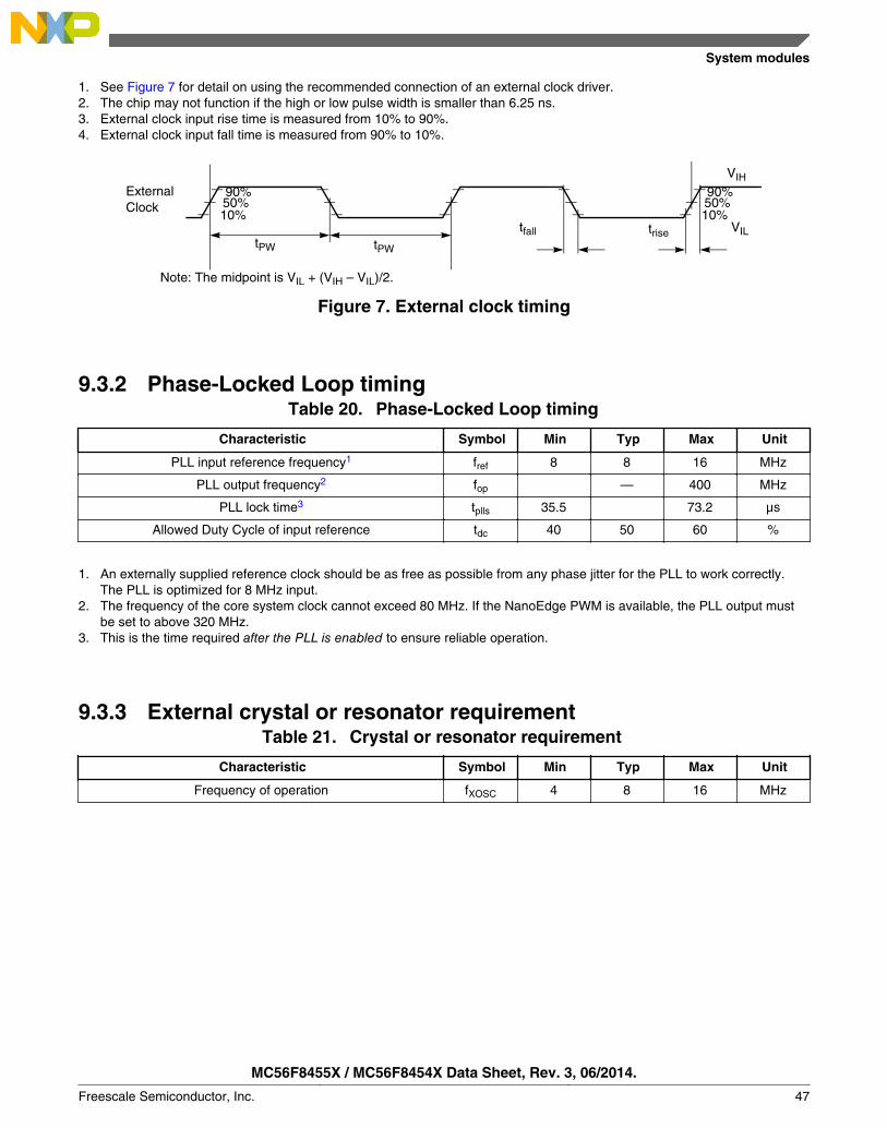
1. See Figure 7 for detail on using the recommended connection of an external clock driver.2. The chip may not function if the high or low pulse width is smaller than 6.25 ns.3. External clock input rise time is measured from 10% to 90%.4. External clock input fall time is measured from 90% to 10%.
90%50%10%
90%50%10%
External Clock
tPW tPW
tfall trise VIL
VIH
Note: The midpoint is VIL + (VIH – VIL)/2.
Figure 7. External clock timing
9.3.2 Phase-Locked Loop timingTable 20. Phase-Locked Loop timing
Characteristic Symbol Min Typ Max Unit
PLL input reference frequency1 fref 8 8 16 MHz
PLL output frequency2 fop — 400 MHz
PLL lock time3 tplls 35.5 73.2 µs
Allowed Duty Cycle of input reference tdc 40 50 60 %
1. An externally supplied reference clock should be as free as possible from any phase jitter for the PLL to work correctly.The PLL is optimized for 8 MHz input.
2. The frequency of the core system clock cannot exceed 80 MHz. If the NanoEdge PWM is available, the PLL output mustbe set to above 320 MHz.
3. This is the time required after the PLL is enabled to ensure reliable operation.
9.3.3 External crystal or resonator requirementTable 21. Crystal or resonator requirement
Characteristic Symbol Min Typ Max Unit
Frequency of operation fXOSC 4 8 16 MHz
System modules
MC56F8455X / MC56F8454X Data Sheet, Rev. 3, 06/2014.
Freescale Semiconductor, Inc. 47
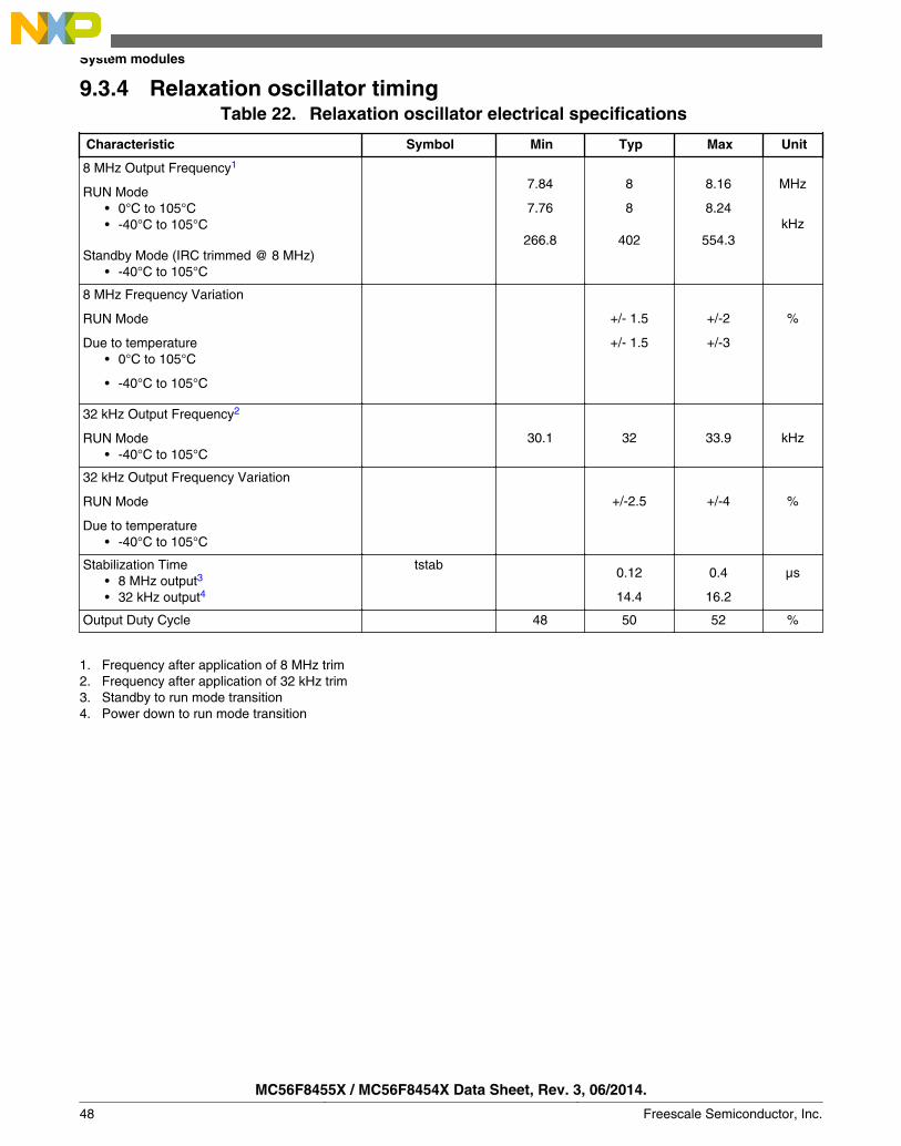
9.3.4 Relaxation oscillator timingTable 22. Relaxation oscillator electrical specifications
Characteristic Symbol Min Typ Max Unit
8 MHz Output Frequency1
RUN Mode• 0°C to 105°C• -40°C to 105°C
Standby Mode (IRC trimmed @ 8 MHz)• -40°C to 105°C
7.84
7.76
266.8
8
8
402
8.16
8.24
554.3
MHz
kHz
8 MHz Frequency Variation
RUN Mode
Due to temperature• 0°C to 105°C
• -40°C to 105°C
+/- 1.5
+/- 1.5
+/-2
+/-3
%
32 kHz Output Frequency2
RUN Mode• -40°C to 105°C
30.1 32 33.9 kHz
32 kHz Output Frequency Variation
RUN Mode
Due to temperature• -40°C to 105°C
+/-2.5 +/-4 %
Stabilization Time• 8 MHz output3
• 32 kHz output4
tstab0.12
14.4
0.4
16.2
µs
Output Duty Cycle 48 50 52 %
1. Frequency after application of 8 MHz trim2. Frequency after application of 32 kHz trim3. Standby to run mode transition4. Power down to run mode transition
System modules
MC56F8455X / MC56F8454X Data Sheet, Rev. 3, 06/2014.
48 Freescale Semiconductor, Inc.
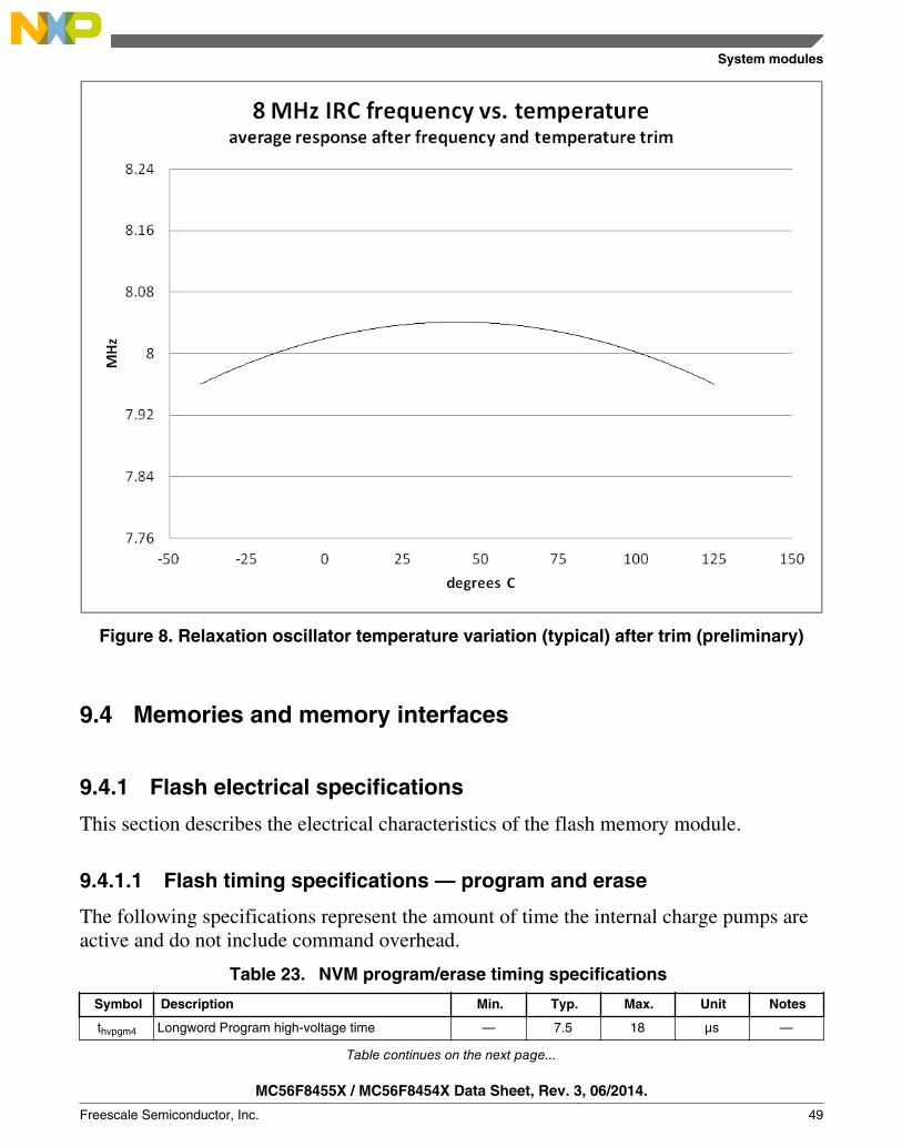
Figure 8. Relaxation oscillator temperature variation (typical) after trim (preliminary)
9.4 Memories and memory interfaces
9.4.1 Flash electrical specifications
This section describes the electrical characteristics of the flash memory module.
9.4.1.1 Flash timing specifications — program and erase
The following specifications represent the amount of time the internal charge pumps areactive and do not include command overhead.
Table 23. NVM program/erase timing specifications
Symbol Description Min. Typ. Max. Unit Notes
thvpgm4 Longword Program high-voltage time — 7.5 18 μs —
Table continues on the next page...
System modules
MC56F8455X / MC56F8454X Data Sheet, Rev. 3, 06/2014.
Freescale Semiconductor, Inc. 49
Table 23. NVM program/erase timing specifications (continued)
Symbol Description Min. Typ. Max. Unit Notes
thversscr Sector Erase high-voltage time — 13 113 ms 1
thversblk32k Erase Block high-voltage time for 32 KB — 52 452 ms 1
thversblk256k Erase Block high-voltage time for 256 KB — 104 904 ms 1
1. Maximum time based on expectations at cycling end-of-life.
9.4.1.2 Flash timing specifications — commandsTable 24. Flash command timing specifications
Symbol Description Min. Typ. Max. Unit Notes
trd1blk32k
trd1blk256k
Read 1s Block execution time
• 32 KB data flash
• 256 KB program flash
—
—
—
—
0.5
1.7
ms
ms
—
trd1sec1k Read 1s Section execution time (data flashsector)
— — 60 μs 1
trd1sec2k Read 1s Section execution time (program flashsector)
— — 60 μs 1
tpgmchk Program Check execution time — — 45 μs 1
trdrsrc Read Resource execution time — — 30 μs 1
tpgm4 Program Longword execution time — 65 145 μs —
tersblk32k
tersblk256k
Erase Flash Block execution time
• 32 KB data flash
• 256 KB program flash
—
—
55
122
465
985
ms
ms
2
tersscr Erase Flash Sector execution time — 14 114 ms 2
tpgmsec512p
tpgmsec512d
tpgmsec1kp
tpgmsec1kd
Program Section execution time
• 512 B program flash
• 512 B data flash
• 1 KB program flash
• 1 KB data flash
—
—
—
—
2.4
4.7
4.7
9.3
—
—
—
—
ms
ms
ms
ms
—
trd1all Read 1s All Blocks execution time — — 1.8 ms —
trdonce Read Once execution time — — 25 μs 1
tpgmonce Program Once execution time — 65 — μs —
tersall Erase All Blocks execution time — 175 1500 ms 2
tvfykey Verify Backdoor Access Key execution time — — 30 μs 1
tpgmpart32k
Program Partition for EEPROM execution time
• 32 KB FlexNVM
—
70
—
ms
—
Table continues on the next page...
System modules
MC56F8455X / MC56F8454X Data Sheet, Rev. 3, 06/2014.
50 Freescale Semiconductor, Inc.
Table 24. Flash command timing specifications (continued)
Symbol Description Min. Typ. Max. Unit Notes
tsetramff
tsetram8k
tsetram32k
Set FlexRAM Function execution time:
• Control Code 0xFF
• 8 KB EEPROM backup
• 32 KB EEPROM backup
—
—
—
50
0.3
0.7
—
0.5
1.0
μs
ms
ms
—
Byte-write to FlexRAM for EEPROM operation
teewr8bers Byte-write to erased FlexRAM location executiontime
— 175 260 μs 3
teewr8b8k
teewr8b16k
teewr8b32k
Byte-write to FlexRAM execution time:
• 8 KB EEPROM backup
• 16 KB EEPROM backup
• 32 KB EEPROM backup
—
—
—
340
385
475
1700
1800
2000
μs
μs
μs
—
Word-write to FlexRAM for EEPROM operation
teewr16bers Word-write to erased FlexRAM locationexecution time
— 175 260 μs —
teewr16b8k
teewr16b16k
teewr16b32k
Word-write to FlexRAM execution time:
• 8 KB EEPROM backup
• 16 KB EEPROM backup
• 32 KB EEPROM backup
—
—
—
340
385
475
1700
1800
2000
μs
μs
μs
—
Longword-write to FlexRAM for EEPROM operation
teewr32bers Longword-write to erased FlexRAM locationexecution time
— 360 540 μs —
teewr32b8k
teewr32b16k
teewr32b32k
Longword-write to FlexRAM execution time:
• 8 KB EEPROM backup
• 16 KB EEPROM backup
• 32 KB EEPROM backup
—
—
—
545
630
810
1950
2050
2250
μs
μs
μs
—
1. Assumes 25 MHz flash clock frequency.2. Maximum times for erase parameters based on expectations at cycling end-of-life.3. For byte-writes to an erased FlexRAM location, the aligned word containing the byte must be erased.
9.4.1.3 Flash high voltage current behaviorsTable 25. Flash high voltage current behaviors
Symbol Description Min. Typ. Max. Unit
IDD_PGM Average current adder during high voltageflash programming operation
— 2.5 6.0 mA
IDD_ERS Average current adder during high voltageflash erase operation
— 1.5 4.0 mA
System modules
MC56F8455X / MC56F8454X Data Sheet, Rev. 3, 06/2014.
Freescale Semiconductor, Inc. 51
9.4.1.4 Reliability specificationsTable 26. NVM reliability specifications
Symbol Description Min. Typ.1 Max. Unit Notes
Program Flash
tnvmretp10k Data retention after up to 10 K cycles 5 50 — years —
tnvmretp1k Data retention after up to 1 K cycles 20 100 — years —
nnvmcycp Cycling endurance 10 K 50 K — cycles 2
Data Flash
tnvmretd10k Data retention after up to 10 K cycles 5 50 — years —
tnvmretd1k Data retention after up to 1 K cycles 20 100 — years —
nnvmcycd Cycling endurance 10 K 50 K — cycles 2
FlexRAM as EEPROM
tnvmretee100 Data retention up to 100% of write endurance 5 50 — years —
tnvmretee10 Data retention up to 10% of write endurance 20 100 — years —
nnvmwree16
nnvmwree128
nnvmwree512
nnvmwree4k
nnvmwree8k
Write endurance
• EEPROM backup to FlexRAM ratio = 16
• EEPROM backup to FlexRAM ratio = 128
• EEPROM backup to FlexRAM ratio = 512
• EEPROM backup to FlexRAM ratio = 4096
• EEPROM backup to FlexRAM ratio = 8192
35 K
315 K
1.27 M
10 M
20 M
175 K
1.6 M
6.4 M
50 M
100 M
—
—
—
—
—
writes
writes
writes
writes
writes
3
1. Typical data retention values are based on measured response accelerated at high temperature and derated to a constant25 °C use profile. Engineering Bulletin EB618 does not apply to this technology. Typical endurance defined in EngineeringBulletin EB619.
2. Cycling endurance represents number of program/erase cycles at -40 °C ≤ Tj ≤ 125 °C.3. Write endurance represents the number of writes to each FlexRAM location at -40 °C ≤Tj ≤ 125 °C influenced by the
cycling endurance of the FlexNVM (same value as data flash) and the allocated EEPROM backup. Minimum and typicalvalues assume all byte-writes to FlexRAM.
9.5 Analog
9.5.1 12-bit cyclic Analog-to-Digital Converter (ADC) parametersTable 27. 12-bit ADC electrical specifications
Characteristic Symbol Min Typ Max Unit
Recommended Operating Conditions
Supply Voltage1 VDDA 2.7 3.3 3.6 V
Vrefh Supply Voltage2 Vrefhx 3.0 VDDA V
ADC Conversion Clock3 fADCCLK 0.6 20 MHz
Conversion Range RAD VREFL VREFH V
Table continues on the next page...
System modules
MC56F8455X / MC56F8454X Data Sheet, Rev. 3, 06/2014.
52 Freescale Semiconductor, Inc.
Table 27. 12-bit ADC electrical specifications (continued)
Characteristic Symbol Min Typ Max Unit
Input Voltage Range
External Reference
Internal Reference
VADIN VREFL
VSSA
VREFH
VDDA
V
Timing and Power
Conversion Time tADC 6 ADC Clock Cycles
Sample Time tADS 1 5 ADC Clock Cycles
ADC Power-Up Time (from adc_pdn) tADPU 13 ADC Clock Cycles
ADC RUN Current (per ADC block)
• at 600 kHz ADC Clock, LP mode
• ≤ 8.33 MHz ADC Clock, 00 mode
• ≤ 12.5 MHz ADC Clock, 01 mode
• ≤ 16.67 MHz ADC Clock, 10 mode
• ≤ 20 MHz ADC Clock, 11 mode
IADRUN1
5.7
10.5
17.7
22.6
mA
ADC Powerdown Current (adc_pdn enabled) IADPWRDWN 0.02 µA
VREFH Current IVREFH 0.001 µA
Accuracy (DC or Absolute)
Integral non-Linearity4 INL +/- 3 +/- 5 LSB5
Differential non-Linearity4 DNL +/- 0.6 +/- 0.9 LSB5
Monotonicity
Offset6
• 1x gain mode• 2x gain mode• 4x gain mode
VOFFSET +/- 17
+/- 20
+/- 25
LSB 4
Gain Error (normalized) EGAIN 0.994 to1.004
0.990 to1.010
AC Specifications7
Signal to Noise Ratio SNR 59 dB
Total Harmonic Distortion THD 64 dB
Spurious Free Dynamic Range SFDR 65 dB
Signal to Noise plus Distortion SINAD 59 dB
Effective Number of Bits ENOB bits
ADC Inputs
Input Leakage Current IIN 0 +/-2 µA
Input Injection Current 8 IINJ +/-3 mA
Input Capacitance
Sampling Capacitor
• 1x mode
• 2x mode
• 4x mode
CADI -
-
1.4
2.8
5.6
pF
System modules
MC56F8455X / MC56F8454X Data Sheet, Rev. 3, 06/2014.
Freescale Semiconductor, Inc. 53
1. If the ADC’s reference is from VDDA: When VDDA is below 3.0 V, then the ADC functions, but the ADC specifications arenot guaranteed.
2. When the input is at the Vrefl level, then the resulting output will be all zeros (hex 000), plus any error contribution due tooffset and gain error. When the input is at the Vrefh level, then the output will be all ones (hex FFF), minus any errorcontribution due to offset and gain error.
3. ADC clock duty cycle min/max is 45/55%4. INL measured from VIN = VREFL to VIN = V
REFH.
5. LSB = Least Significant Bit = 0.806 mV at 3.3 V VDDA, x1 Gain Setting6. Offset over the conversion range of 0025 to 4080, with internal/external reference.7. Measured when converting a 1 kHz input Full Scale sine wave.8. The current that can be injected into or sourced from an unselected ADC input, without affecting the performance of the
ADC.
9.5.1.1 Equivalent circuit for ADC inputs
The following figure shows the ADC input circuit during sample and hold. S1 and S2 arealways opened/closed at non-overlapping phases, and both S1 and S2 operate at the ADCclock frequency. The following equation gives equivalent input impedance when theinput is selected.
Freescale Semiconductor32
1
(ADC ClockRate) x 1.4x10⁻¹² + 100ohm + 125ohm
1 2 3
Analog Input
S1
S1
S2
C1
C1
S/H
C1: Single Ended Mode2XC1: Differential Mode
(VREFHx - VREFLx ) / 2
125 ESDResistor
S2
S1
S1
Channel Muxequivalent resistance
100Ohms
C1: Single Ended Mode2XC1: Differential Mode
1. Parasitic capacitance due to package, pin-to-pin and pin-to-package base coupling =1.8pF
2. Parasitic capacitance due to the chip bond pad, ESD protection devices and signalrouting = 2.04pF
3. 8 pF noise damping capacitor4. Sampling capacitor at the sample and hold circuit. Capacitor C1 (4.8pF) is normally
disconnected from the input, and is only connected to the input at sampling time.5. S1 and S2 switch phases are non-overlapping and operate at the ADC clock
frequency
System modules
MC56F8455X / MC56F8454X Data Sheet, Rev. 3, 06/2014.
54 Freescale Semiconductor, Inc.
S 1
S 2
Figure 9. Equivalent circuit for A/D loading
9.5.2 16-bit SAR ADC electrical specifications
9.5.2.1 16-bit ADC operating conditionsTable 28. 16-bit ADC operating conditions
Symbol Description Conditions Min. Typ.1 Max. Unit Notes
VDDA Supply voltage Absolute 2.7 — 3.6 V —
ΔVDDA Supply voltage Delta to VDD (VDD – VDDA) -100 0 +100 mV 2
ΔVSSA Ground voltage Delta to VSS (VSS – VSSA) -100 0 +100 mV 2
VREFH ADC referencevoltage high
Absolute VDDA VDDA VDDA V 3
VREFL ADC referencevoltage low
Absolute VSSA VSSA VSSA V 4
VADIN Input voltage VSSA — VDDA V —
CADIN Input capacitance • 16-bit mode
• 8-bit / 10-bit / 12-bitmodes
—
—
8
4
10
5
pF —
RADIN Input seriesresistance
— 2 5 kΩ —
RAS Analog sourceresistance(external)
12-bit modes
fADCK < 4 MHz
—
—
5
kΩ
5
fADCK ADC conversionclock frequency
≤ 12-bit mode 1.0 — 18.0 MHz 6
fADCK ADC conversionclock frequency
16-bit mode 2.0 — 12.0 MHz 6
Crate ADC conversionrate
≤ 12-bit modes
No ADC hardware averaging
Continuous conversionsenabled, subsequentconversion time
20.000
—
818.330
Ksps
7
Crate ADC conversionrate
16-bit mode
No ADC hardware averaging
Continuous conversionsenabled, subsequentconversion time
37.037
—
461.467
Ksps
7
1. Typical values assume VDDA = 3.0 V, Temp = 25 °C, fADCK = 1.0 MHz, unless otherwise stated. Typical values are forreference only, and are not tested in production.
2. DC potential difference.
System modules
MC56F8455X / MC56F8454X Data Sheet, Rev. 3, 06/2014.
Freescale Semiconductor, Inc. 55
3. VREFH is internally tied to VDDA.4. VREFL is internally tied to VSSA.5. This resistance is external to MCU. To achieve the best results, the analog source resistance must be kept as low as
possible. The results in this data sheet were derived from a system that had < 8 Ω analog source resistance. The RAS/CAStime constant should be kept to < 1 ns.
6. To use the maximum ADC conversion clock frequency, CFG2[ADHSC] must be set and CFG1[ADLPC] must be clear.7. For guidelines and examples of conversion rate calculation, download the ADC calculator tool.
RAS
VAS CAS
ZAS
VADIN
ZADIN
RADIN
RADIN
RADIN
RADIN
CADIN
Pad leakagedue toinput protection
INPUT PIN
INPUT PIN
INPUT PIN
SIMPLIFIEDINPUT PIN EQUIVALENT
CIRCUITSIMPLIFIED
CHANNEL SELECTCIRCUIT ADC SAR
ENGINE
Figure 10. ADC input impedance equivalency diagram
9.5.2.2 16-bit ADC electrical characteristicsTable 29. 16-bit ADC characteristics (VREFH = VDDA, VREFL = VSSA)
Symbol Description Conditions1 Min. Typ.2 Max. Unit Notes
IDDA_ADC Supply current — 1.7 mA 3
fADACK
ADCasynchronousclock source
• ADLPC=1, ADHSC=0
• ADLPC=1, ADHSC=1
• ADLPC=0, ADHSC=0
• ADLPC=0, ADHSC=1
1.2
3.0
2.4
4.4
2.4
4.0
5.2
6.2
3.9
7.3
6.1
9.5
MHz
MHz
MHz
MHz
tADACK = 1/fADACK
Sample Time See Reference Manual chapter for sample times
TUE Total unadjustederror
• 12-bit modes
• <12-bit modes
—
—
±4
±1.4
±6.8
±2.1
LSB4 5
DNL Differential non-linearity
• 16-bit modes
• 12-bit modes
• <12-bit modes
—
—
—
-1 to +4
±0.7
±0.2
—
—
-0.3 to 0.5
LSB4 5
Table continues on the next page...
System modules
MC56F8455X / MC56F8454X Data Sheet, Rev. 3, 06/2014.
56 Freescale Semiconductor, Inc.
Table 29. 16-bit ADC characteristics (VREFH = VDDA, VREFL = VSSA) (continued)
Symbol Description Conditions1 Min. Typ.2 Max. Unit Notes
INL Integral non-linearity
• 16-bit modes
• 12-bit modes
• <12-bit modes
—
—
—
±7.0
±1.0
±0.5
—
-2.7 to +1.9
-0.7 to +0.5
LSB4 5
EFS Full-scale error • 12-bit modes
• <12-bit modes
—
—
-4
-1.4
-5.4
-1.8
LSB4 VADIN =VDDA
5
EQ Quantizationerror
• 16-bit modes
• 12-bit modes
—
—
-1 to 0
—
—
±0.5
LSB4
ENOB Effective numberof bits
16-bit single-ended mode
• Avg=32
• Avg=4
12-bit single-ended mode
• Avg=32
• Avg=1
12.2
11.4
13.9
13.1
10.8
10.2
—
—
—
—
bits
bits
bits
bits
6
SINADSignal-to-noiseplus distortion
See ENOB6.02 × ENOB + 1.76 dB
THD Total harmonicdistortion
16-bit single-ended mode
• Avg=32
12-bit single-ended mode
• Avg=32
—
—
-85
-74
—
—
dB
dB
7
SFDR Spurious freedynamic range
16-bit single-ended mode
• Avg=32
12-bit single-ended mode
• Avg=32
78
90
78
—
—
dB
dB
7
EIL Input leakageerror
IIn × RAS mV IIn =leakagecurrent
(refer tothe
device'svoltage
and currentoperatingratings)
Temp sensorslope
–40°C to 105°C — 1.715 — mV/°C
VTEMP25 Temp sensorvoltage
25°C — 722 — mV 8
1. All accuracy numbers assume the ADC is calibrated with VREFH = VDDA
System modules
MC56F8455X / MC56F8454X Data Sheet, Rev. 3, 06/2014.
Freescale Semiconductor, Inc. 57
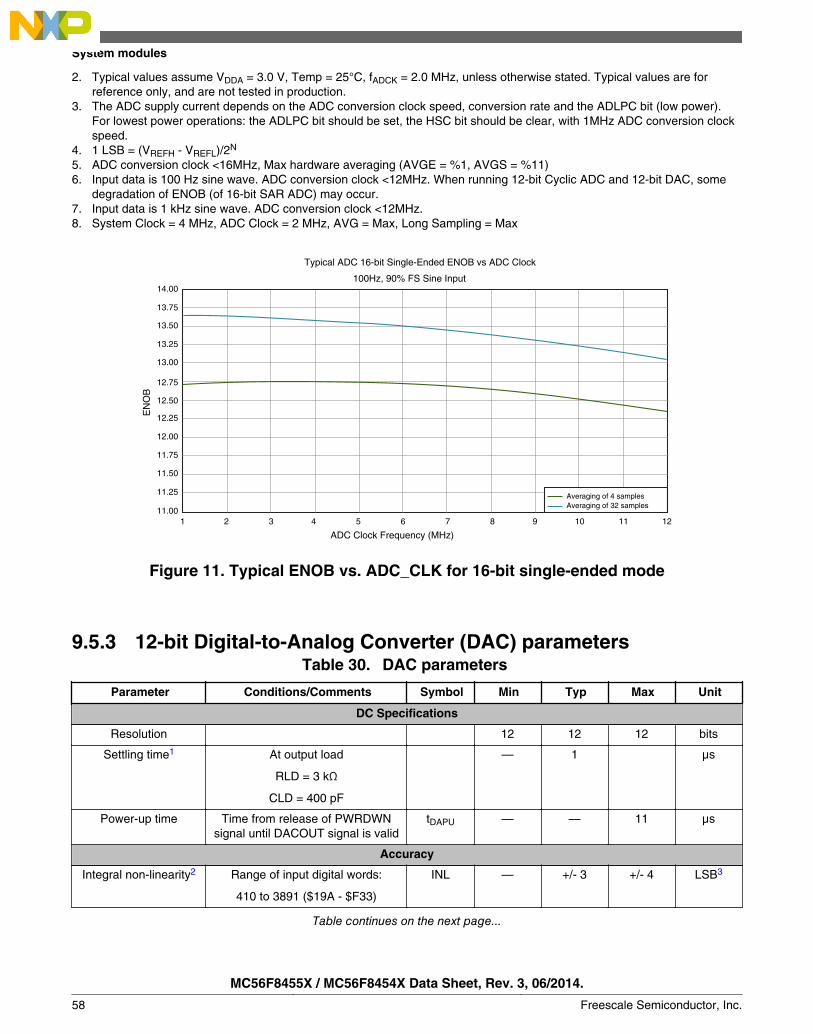
2. Typical values assume VDDA = 3.0 V, Temp = 25°C, fADCK = 2.0 MHz, unless otherwise stated. Typical values are forreference only, and are not tested in production.
3. The ADC supply current depends on the ADC conversion clock speed, conversion rate and the ADLPC bit (low power).For lowest power operations: the ADLPC bit should be set, the HSC bit should be clear, with 1MHz ADC conversion clockspeed.
4. 1 LSB = (VREFH - VREFL)/2N
5. ADC conversion clock <16MHz, Max hardware averaging (AVGE = %1, AVGS = %11)6. Input data is 100 Hz sine wave. ADC conversion clock <12MHz. When running 12-bit Cyclic ADC and 12-bit DAC, some
degradation of ENOB (of 16-bit SAR ADC) may occur.7. Input data is 1 kHz sine wave. ADC conversion clock <12MHz.8. System Clock = 4 MHz, ADC Clock = 2 MHz, AVG = Max, Long Sampling = Max
Typical ADC 16-bit Single-Ended ENOB vs ADC Clock
100Hz, 90% FS Sine Input
EN
OB
ADC Clock Frequency (MHz)
14.00
13.75
13.25
13.00
12.75
12.50
12.00
11.75
11.50
11.25
11.001 2 3 4 5 6 7 8 9 10 1211
Averaging of 4 samplesAveraging of 32 samples
13.50
12.25
Figure 11. Typical ENOB vs. ADC_CLK for 16-bit single-ended mode
9.5.3 12-bit Digital-to-Analog Converter (DAC) parametersTable 30. DAC parameters
Parameter Conditions/Comments Symbol Min Typ Max Unit
DC Specifications
Resolution 12 12 12 bits
Settling time1 At output load
RLD = 3 kΩ
CLD = 400 pF
— 1 µs
Power-up time Time from release of PWRDWNsignal until DACOUT signal is valid
tDAPU — — 11 µs
Accuracy
Integral non-linearity2 Range of input digital words:
410 to 3891 ($19A - $F33)
INL — +/- 3 +/- 4 LSB3
Table continues on the next page...
System modules
MC56F8455X / MC56F8454X Data Sheet, Rev. 3, 06/2014.
58 Freescale Semiconductor, Inc.
Table 30. DAC parameters (continued)
Parameter Conditions/Comments Symbol Min Typ Max Unit
Differential non-linearity2
Range of input digital words:
410 to 3891 ($19A - $F33)
DNL — +/- 0.8 +/- 0.9 LSB3
Monotonicity > 6 sigma monotonicity,
< 3.4 ppm non-monotonicity
guaranteed —
Offset error2 Range of input digital words:
410 to 3891 ($19A - $F33)
VOFFSET — +/- 25 +/- 43 mV
Gain error2 Range of input digital words: 410 to3891 ($19A - $F33)
EGAIN — +/- 0.5 +/- 1.5 %
DAC Output
Output voltage range Within 40 mV of either VSSA or VDDA VOUT VSSA +0.04 V
— VDDA - 0.04V
V
AC Specifications
Signal-to-noise ratio SNR — 85 — dB
Spurious free dynamicrange
SFDR — -72 — dB
Effective number of bits ENOB — 11 — bits
1. Settling time is swing range from VSSA to VDDA2. No guaranteed specification within 5% of VDDA or VSSA3. LSB = 0.806 mV
9.5.4 CMP and 6-bit DAC electrical specificationsTable 31. Comparator and 6-bit DAC electrical specifications
Symbol Description Min. Typ. Max. Unit
VDD Supply voltage 2.7 — 3.6 V
IDDHS Supply current, high-speed mode (EN=1, PMODE=1) — — 200 μA
IDDLS Supply current, low-speed mode (EN=1, PMODE=0) — — 20 μA
VAIN Analog input voltage VSS – 0.3 — VDD V
VAIO Analog input offset voltage — — 20 mV
VH Analog comparator hysteresis1
• CR0[HYSTCTR] = 00
• CR0[HYSTCTR] = 01
• CR0[HYSTCTR] = 10
• CR0[HYSTCTR] = 11
—
—
—
—
5
10
20
30
13
48
105
148
mV
mV
mV
mV
VCMPOh Output high VDD – 0.5 — — V
VCMPOl Output low — — 0.5 V
tDHS Propagation delay, high-speed mode (EN=1,PMODE=1)2
50 ns
Table continues on the next page...
System modules
MC56F8455X / MC56F8454X Data Sheet, Rev. 3, 06/2014.
Freescale Semiconductor, Inc. 59
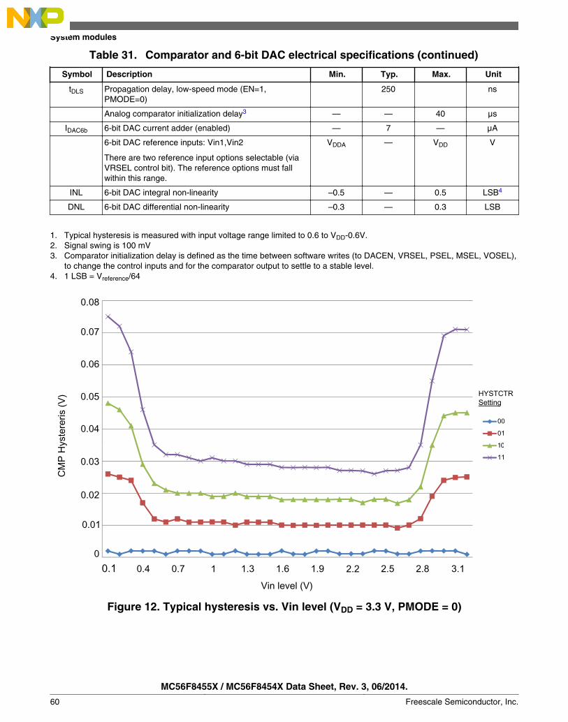
Table 31. Comparator and 6-bit DAC electrical specifications (continued)
Symbol Description Min. Typ. Max. Unit
tDLS Propagation delay, low-speed mode (EN=1,PMODE=0)
250 ns
Analog comparator initialization delay3 — — 40 μs
IDAC6b 6-bit DAC current adder (enabled) — 7 — μA
6-bit DAC reference inputs: Vin1,Vin2
There are two reference input options selectable (viaVRSEL control bit). The reference options must fallwithin this range.
VDDA — VDD V
INL 6-bit DAC integral non-linearity –0.5 — 0.5 LSB4
DNL 6-bit DAC differential non-linearity –0.3 — 0.3 LSB
1. Typical hysteresis is measured with input voltage range limited to 0.6 to VDD-0.6V.2. Signal swing is 100 mV3. Comparator initialization delay is defined as the time between software writes (to DACEN, VRSEL, PSEL, MSEL, VOSEL),
to change the control inputs and for the comparator output to settle to a stable level.4. 1 LSB = Vreference/64
00
01
10
HYSTCTR Setting
0.1
10
11
Vin level (V)
CM
P H
yste
reris
(V)
3.12.82.52.21.91.61.310.70.4
0.05
0
0.01
0.02
0.03
0.08
0.07
0.06
0.04
Figure 12. Typical hysteresis vs. Vin level (VDD = 3.3 V, PMODE = 0)
System modules
MC56F8455X / MC56F8454X Data Sheet, Rev. 3, 06/2014.
60 Freescale Semiconductor, Inc.

000110
HYSTCTR Setting
1011
0.1 3.12.82.52.21.91.61.310.70.4
0.1
0
0.02
0.04
0.06
0.18
0.14
0.12
0.08
0.16
Vin level (V)
CM
P H
yste
resi
s (V
)
Figure 13. Typical hysteresis vs. Vin level (VDD = 3.3 V, PMODE = 1)
PWMs and timers
9.6.1 Enhanced NanoEdge PWM characteristicsTable 32. NanoEdge PWM timing parameters
Characteristic Symbol Min Typ Max Unit
PWM clock frequency 77.5 80 82.5 MHz
NanoEdge Placement (NEP) Step Size1, 2 pwmp 390 ps
Delay for fault input activating to PWM output deactivated 1 ns
Power-up Time3 tpu 25 µs
1. Reference IPbus clock of 80 MHz in NanoEdge Placement mode.2. Temperature and voltage variations do not affect NanoEdge Placement step size.3. Powerdown to NanoEdge mode transition.
9.6
PWMs and timers
MC56F8455X / MC56F8454X Data Sheet, Rev. 3, 06/2014.
Freescale Semiconductor, Inc. 61
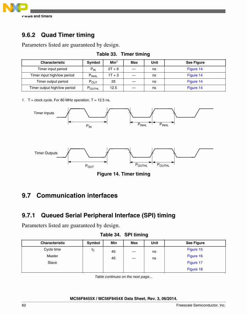
9.6.2 Quad Timer timing
Parameters listed are guaranteed by design.
Table 33. Timer timing
Characteristic Symbol Min1 Max Unit See Figure
Timer input period PIN 2T + 6 — ns Figure 14
Timer input high/low period PINHL 1T + 3 — ns Figure 14
Timer output period POUT 25 — ns Figure 14
Timer output high/low period POUTHL 12.5 — ns Figure 14
1. T = clock cycle. For 80 MHz operation, T = 12.5 ns.
POUTPOUTHL POUTHL
PINPINHL PINHL
Timer Inputs
Timer Outputs
Figure 14. Timer timing
9.7 Communication interfaces
9.7.1 Queued Serial Peripheral Interface (SPI) timing
Parameters listed are guaranteed by design.
Table 34. SPI timing
Characteristic Symbol Min Max Unit See Figure
Cycle time
Master
Slave
tC 45
45
—
—
ns
ns
Figure 15
Figure 16
Figure 17
Figure 18
Table continues on the next page...
PWMs and timers
MC56F8455X / MC56F8454X Data Sheet, Rev. 3, 06/2014.
62 Freescale Semiconductor, Inc.
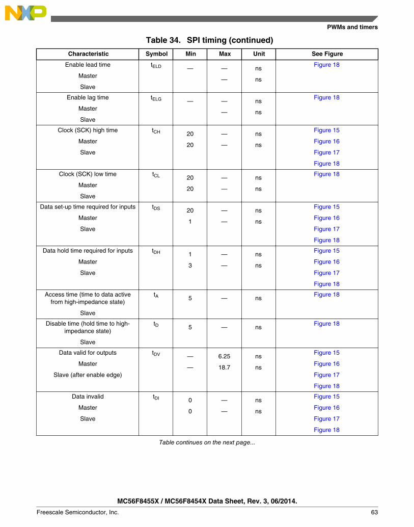
Table 34. SPI timing (continued)
Characteristic Symbol Min Max Unit See Figure
Enable lead time
Master
Slave
tELD — —
—
ns
ns
Figure 18
Enable lag time
Master
Slave
tELG — —
—
ns
ns
Figure 18
Clock (SCK) high time
Master
Slave
tCH 20
20
—
—
ns
ns
Figure 15
Figure 16
Figure 17
Figure 18
Clock (SCK) low time
Master
Slave
tCL 20
20
—
—
ns
ns
Figure 18
Data set-up time required for inputs
Master
Slave
tDS 20
1
—
—
ns
ns
Figure 15
Figure 16
Figure 17
Figure 18
Data hold time required for inputs
Master
Slave
tDH 1
3
—
—
ns
ns
Figure 15
Figure 16
Figure 17
Figure 18
Access time (time to data activefrom high-impedance state)
Slave
tA 5 — nsFigure 18
Disable time (hold time to high-impedance state)
Slave
tD 5 — nsFigure 18
Data valid for outputs
Master
Slave (after enable edge)
tDV —
—
6.25
18.7
ns
ns
Figure 15
Figure 16
Figure 17
Figure 18
Data invalid
Master
Slave
tDI 0
0
—
—
ns
ns
Figure 15
Figure 16
Figure 17
Figure 18
Table continues on the next page...
PWMs and timers
MC56F8455X / MC56F8454X Data Sheet, Rev. 3, 06/2014.
Freescale Semiconductor, Inc. 63
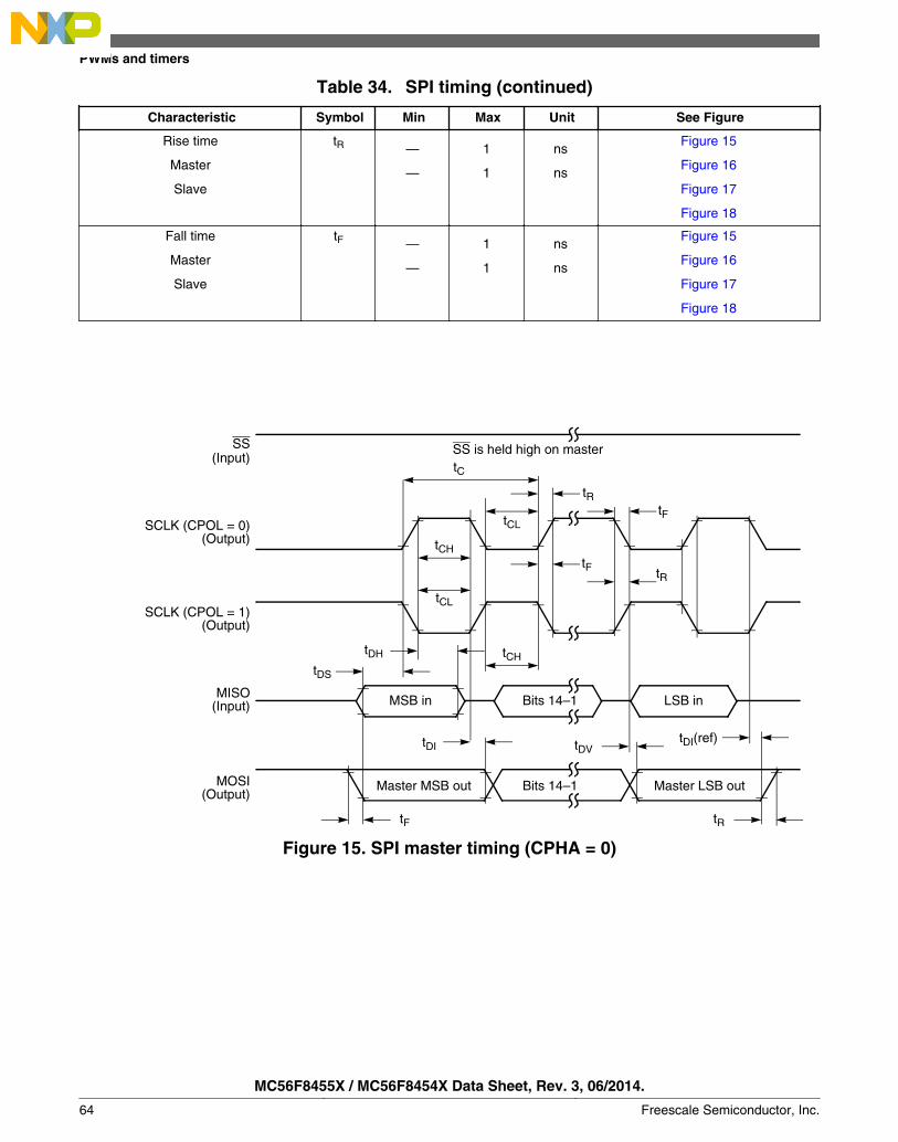
Table 34. SPI timing (continued)
Characteristic Symbol Min Max Unit See Figure
Rise time
Master
Slave
tR —
—
1
1
ns
ns
Figure 15
Figure 16
Figure 17
Figure 18
Fall time
Master
Slave
tF —
—
1
1
ns
ns
Figure 15
Figure 16
Figure 17
Figure 18
SCLK (CPOL = 0)(Output)
SCLK (CPOL = 1)(Output)
MISO(Input)
MOSI(Output)
MSB in Bits 14–1 LSB in
tF
tC
tCL
tCL
tR
tRtF
tDS
tDH tCH
tDI tDVtDI(ref)
tR
Master MSB out Bits 14–1 Master LSB out
SS(Input)
tCH
SS is held high on master
tF
Figure 15. SPI master timing (CPHA = 0)
PWMs and timers
MC56F8455X / MC56F8454X Data Sheet, Rev. 3, 06/2014.
64 Freescale Semiconductor, Inc.
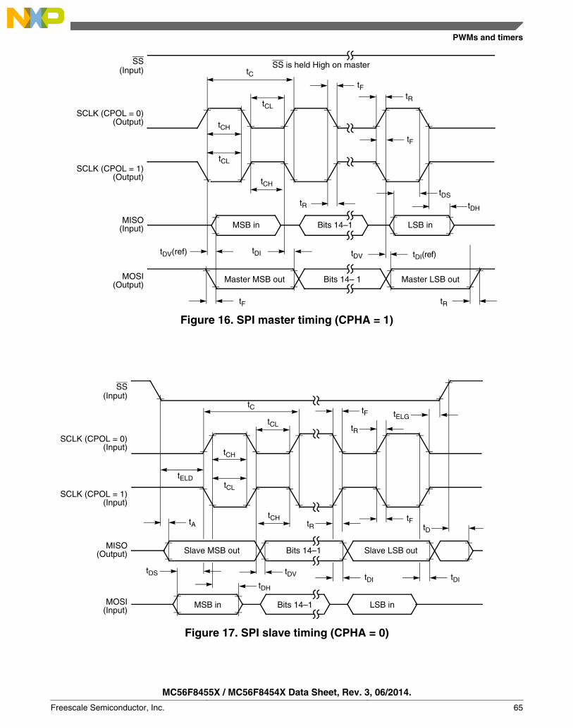
SCLK (CPOL = 0)(Output)
SCLK (CPOL = 1)(Output)
MISO(Input)
MOSI(Output)
MSB in Bits 14–1 LSB in
tR
tC
tCL
tCL
tF
tCH
tDV(ref) tDV tDI(ref)
tRtF
Master MSB out Bits 14– 1 Master LSB out
SS(Input)
tCH
SS is held High on master
tDS
tDH
tDI
tR
tF
Figure 16. SPI master timing (CPHA = 1)
SCLK (CPOL = 0)(Input)
SCLK (CPOL = 1)(Input)
MISO(Output)
MOSI(Input)
Slave MSB out Bits 14–1
tC
tCL
tCL
tF
tCH
tDI
MSB in Bits 14–1 LSB in
SS(Input)
tCH
tDH
tR
tELG
tELD
tF
Slave LSB out
tDtA
tDS tDV tDI
tR
Figure 17. SPI slave timing (CPHA = 0)
PWMs and timers
MC56F8455X / MC56F8454X Data Sheet, Rev. 3, 06/2014.
Freescale Semiconductor, Inc. 65

SCLK (CPOL = 0)(Input)
SCLK (CPOL = 1)(Input)
MISO(Output)
MOSI(Input)
Slave MSB out Bits 14–1
tC
tCL
tCL
tCH
tDI
MSB in Bits 14–1 LSB in
SS(Input)
tCH
tDH
tF
tR
Slave LSB out
tDtA
tELD
tDV
tF
tR
tELG
tDV
tDS
Figure 18. SPI slave timing (CPHA = 1)
9.7.2 Queued Serial Communication Interface (SCI) timing
Parameters listed are guaranteed by design.
Table 35. SCI timing
Characteristic Symbol Min Max Unit See Figure
Baud rate1 BR — (fMAX/16) Mbit/s —
RXD pulse width RXDPW 0.965/BR 1.04/BR ns Figure 19
TXD pulse width TXDPW 0.965/BR 1.04/BR ns Figure 20
LIN Slave Mode
Deviation of slave node clock from nominalclock rate before synchronization
FTOL_UNSYNCH -14 14 % —
Deviation of slave node clock relative tothe master node clock after
synchronization
FTOL_SYNCH -2 2 % —
Minimum break character length TBREAK 13 — Masternode bitperiods
—
11 — Slave nodebit periods
—
1. fMAX is the frequency of operation of the SCI clock in MHz, which can be selected as the bus clock (max.160 MHzdepending on part number) or 2x bus clock (max. MHz) for the devices.
PWMs and timers
MC56F8455X / MC56F8454X Data Sheet, Rev. 3, 06/2014.
66 Freescale Semiconductor, Inc.
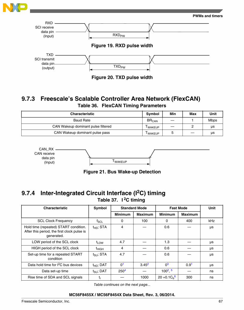
RXDPW
RXD SCI receive
data pin(Input)
Figure 19. RXD pulse width
TXDPW
TXD SCI transmit
data pin(output)
Figure 20. TXD pulse width
9.7.3 Freescale’s Scalable Controller Area Network (FlexCAN)Table 36. FlexCAN Timing Parameters
Characteristic Symbol Min Max Unit
Baud Rate BRCAN — 1 Mbps
CAN Wakeup dominant pulse filtered TWAKEUP — 2 µs
CAN Wakeup dominant pulse pass TWAKEUP 5 — µs
TWAKEUP
CAN_RX CAN receive
data pin(Input)
Figure 21. Bus Wake-up Detection
9.7.4 Inter-Integrated Circuit Interface (I2C) timingTable 37. I 2C timing
Characteristic Symbol Standard Mode Fast Mode Unit
Minimum Maximum Minimum Maximum
SCL Clock Frequency fSCL 0 100 0 400 kHz
Hold time (repeated) START condition.After this period, the first clock pulse is
generated.
tHD; STA 4 — 0.6 — µs
LOW period of the SCL clock tLOW 4.7 — 1.3 — µs
HIGH period of the SCL clock tHIGH 4 — 0.6 — µs
Set-up time for a repeated STARTcondition
tSU; STA 4.7 — 0.6 — µs
Data hold time for I2C bus devices tHD; DAT 01 3.452 03 0.91 µs
Data set-up time tSU; DAT 2504 — 1002, 5 — ns
Rise time of SDA and SCL signals tr — 1000 20 +0.1Cb6 300 ns
Table continues on the next page...
PWMs and timers
MC56F8455X / MC56F8454X Data Sheet, Rev. 3, 06/2014.
Freescale Semiconductor, Inc. 67
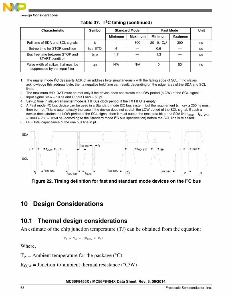
Table 37. I 2C timing (continued)
Characteristic Symbol Standard Mode Fast Mode Unit
Minimum Maximum Minimum Maximum
Fall time of SDA and SCL signals tf — 300 20 +0.1Cb5 300 ns
Set-up time for STOP condition tSU; STO 4 — 0.6 — µs
Bus free time between STOP andSTART condition
tBUF 4.7 — 1.3 — µs
Pulse width of spikes that must besuppressed by the input filter
tSP N/A N/A 0 50 ns
1. The master mode I2C deasserts ACK of an address byte simultaneously with the falling edge of SCL. If no slavesacknowledge this address byte, then a negative hold time can result, depending on the edge rates of the SDA and SCLlines.
2. The maximum tHD; DAT must be met only if the device does not stretch the LOW period (tLOW) of the SCL signal.3. Input signal Slew = 10 ns and Output Load = 50 pF4. Set-up time in slave-transmitter mode is 1 IPBus clock period, if the TX FIFO is empty.5. A Fast mode I2C bus device can be used in a Standard mode I2C bus system, but the requirement tSU; DAT ≥ 250 ns must
then be met. This is automatically the case if the device does not stretch the LOW period of the SCL signal. If such adevice does stretch the LOW period of the SCL signal, then it must output the next data bit to the SDA line trmax + tSU; DAT= 1000 + 250 = 1250 ns (according to the Standard mode I2C bus specification) before the SCL line is released.
6. Cb = total capacitance of the one bus line in pF.
SDA
SCL
tHD; STAtHD; DAT
tLOW
tSU; DAT
tHIGH
tSU; STASR P SS
tHD; STA tSP
tSU; STO
tBUFtf trtf
tr
Figure 22. Timing definition for fast and standard mode devices on the I2C bus
Design Considerations
10.1 Thermal design considerationsAn estimate of the chip junction temperature (TJ) can be obtained from the equation:
TJ = TA + (RΘJA x PD)
Where,
TA = Ambient temperature for the package (°C)
RΘJA = Junction-to-ambient thermal resistance (°C/W)
10
Design Considerations
MC56F8455X / MC56F8454X Data Sheet, Rev. 3, 06/2014.
68 Freescale Semiconductor, Inc.
PD = Power dissipation in the package (W)
The junction-to-ambient thermal resistance is an industry-standard value that provides aquick and easy estimation of thermal performance. Unfortunately, there are two values incommon usage: the value determined on a single-layer board and the value obtained on aboard with two planes. For packages such as the PBGA, these values can be different bya factor of two. Which TJ value is closer to the application depends on the powerdissipated by other components on the board.
• The TJ value obtained on a single layer board is appropriate for a tightly packedprinted circuit board.
• The TJ value obtained on a board with the internal planes is usually appropriate if theboard has low-power dissipation and if the components are well separated.
When a heat sink is used, the thermal resistance is expressed as the sum of a junction-to-case thermal resistance and a case-to-ambient thermal resistance:
RΘJA = RΘJC + RΘCA
Where,
RΘJA = Package junction-to-ambient thermal resistance (°C/W)
RΘJC = Package junction-to-case thermal resistance (°C/W)
RΘCA = Package case-to-ambient thermal resistance (°C/W)
RΘJC is device related and cannot be adjusted. You control the thermal environment tochange the case to ambient thermal resistance, RΘCA. For instance, you can change thesize of the heat sink, the air flow around the device, the interface material, the mountingarrangement on printed circuit board, or change the thermal dissipation on the printedcircuit board surrounding the device.
To determine the junction temperature of the device in the application when heatsinks are not used, the thermal characterization parameter (YJT) can be used todetermine the junction temperature with a measurement of the temperature at the topcenter of the package case using the following equation:
TJ = TT + (ΨJT x PD)
Where,
TT = Thermocouple temperature on top of package (°C/W)
ΨJT = hermal characterization parameter (°C/W)
PD = Power dissipation in package (W)
Design Considerations
MC56F8455X / MC56F8454X Data Sheet, Rev. 3, 06/2014.
Freescale Semiconductor, Inc. 69
The thermal characterization parameter is measured per JESD51–2 specification using a40-gauge type T thermocouple epoxied to the top center of the package case. Thethermocouple should be positioned so that the thermocouple junction rests on thepackage. A small amount of epoxy is placed over the thermocouple junction and overabout 1 mm of wire extending from the junction. The thermocouple wire is placed flatagainst the package case to avoid measurement errors caused by cooling effects of thethermocouple wire.
To determine the junction temperature of the device in the application when heatsinks are used, the junction temperature is determined from a thermocouple inserted atthe interface between the case of the package and the interface material. A clearance slotor hole is normally required in the heat sink. Minimizing the size of the clearance isimportant to minimize the change in thermal performance caused by removing part of thethermal interface to the heat sink. Because of the experimental difficulties with thistechnique, many engineers measure the heat sink temperature and then back-calculate thecase temperature using a separate measurement of the thermal resistance of the interface.From this case temperature, the junction temperature is determined from the junction-to-case thermal resistance.
10.2 Electrical design considerations
CAUTIONThis device contains protective circuitry to guard againstdamage due to high static voltage or electrical fields. However,take normal precautions to avoid application of any voltageshigher than maximum-rated voltages to this high-impedancecircuit. Reliability of operation is enhanced if unused inputs aretied to an appropriate voltage level.
Use the following list of considerations to assure correct operation of the device:• Provide a low-impedance path from the board power supply to each VDD pin on the
device and from the board ground to each VSS (GND) pin.• The minimum bypass requirement is to place 0.01–0.1 µF capacitors positioned as
near as possible to the package supply pins. The recommended bypass configurationis to place one bypass capacitor on each of the VDD/VSS pairs, including VDDA/VSSA.Ceramic and tantalum capacitors tend to provide better tolerances.
• Ensure that capacitor leads and associated printed circuit traces that connect to thechip VDD and VSS (GND) pins are as short as possible.
• Bypass the VDD and VSS with approximately 100 µF, plus the number of 0.1 µFceramic capacitors.
• PCB trace lengths should be minimal for high-frequency signals.
Design Considerations
MC56F8455X / MC56F8454X Data Sheet, Rev. 3, 06/2014.
70 Freescale Semiconductor, Inc.
• Consider all device loads as well as parasitic capacitance due to PCB traces whencalculating capacitance. This is especially critical in systems with higher capacitiveloads that could create higher transient currents in the VDD and VSS circuits.
• Take special care to minimize noise levels on the VREF, VDDA, and VSSA pins.• Using separate power planes for VDD and VDDA and separate ground planes for VSS
and VSSA are recommended. Connect the separate analog and digital power andground planes as near as possible to power supply outputs. If an analog circuit anddigital circuit are powered by the same power supply, then connect a small inductoror ferrite bead in serial with VDDA. Traces of VSS and VSSA should be shortedtogether.
• Physically separate analog components from noisy digital components by groundplanes. Do not place an analog trace in parallel with digital traces. Place an analogground trace around an analog signal trace to isolate it from digital traces.
• Because the flash memory is programmed through the JTAG/EOnCE port, SPI, SCI,or I2C, the designer should provide an interface to this port if in-circuit flashprogramming is desired.
• If desired, connect an external RC circuit to the RESET pin. The resistor valueshould be in the range of 4.7 kΩ–10 kΩ; the capacitor value should be in the range of0.22 µF–4.7 µF.
• Configuring the RESET pin to GPIO output in normal operation in a high-noiseenvironment may help to improve the performance of noise transient immunity.
• Add a 2.2 kΩ external pullup on the TMS pin of the JTAG port to keep EOnCE in arestate during normal operation if JTAG converter is not present.
• During reset and after reset but before I/O initialization, all I/O pins are at tri-state.• To eliminate PCB trace impedance effect, each ADC input should have a no less than
33 pF 10Ω RC filter.
11 Obtaining package dimensionsPackage dimensions are provided in package drawings.
To find a package drawing, go to freescale.com and perform a keyword search for thedrawing’s document number:
Drawing for package Document number to be used
48-pin LQFP 98ASH00962A
64-pin LQFP 98ASS23234W
Obtaining package dimensions
MC56F8455X / MC56F8454X Data Sheet, Rev. 3, 06/2014.
Freescale Semiconductor, Inc. 71
12 Pinout
12.1 Signal Multiplexing and Pin Assignments
This section shows the signals available on each package pin and the locations of thesepins on the devices supported by this document. The SIM's GPS registers are responsiblefor selecting which ALT functionality is available on most pins.
NOTEThe RESETB pin is a 3.3 V pin only.
NOTEIf the GPIOC1 pin is used as GPIO, the XOSC should bepowered down.
NOTEPWMB signals—including PWMB_2A, PWMB_2B, andPWMB_3X—are not available on the 64 LQFP package or the48 LQFP package.
64LQFP
48LQFP
Pin Name Default ALT0 ALT1 ALT2 ALT3
1 1 TCK TCK GPIOD2
2 2 RESETB RESETB GPIOD4
3 3 GPIOC0 GPIOC0 EXTAL CLKIN0
4 4 GPIOC1 GPIOC1 XTAL
5 5 GPIOC2 GPIOC2 TXD0 TB0 XB_IN2 CLKO0
6 — GPIOF8 GPIOF8 RXD0 TB1 CMPD_O
7 6 GPIOC3 GPIOC3 TA0 CMPA_O RXD0 CLKIN1
8 7 GPIOC4 GPIOC4 TA1 CMPB_O XB_IN8 EWM_OUT_B
9 — GPIOA7 GPIOA7 ANA7&ANC11
10 — GPIOA6 GPIOA6 ANA6&ANC10
11 — GPIOA5 GPIOA5 ANA5&ANC9
12 8 GPIOA4 GPIOA4 ANA4&ANC8&CMPD_IN0
13 9 GPIOA0 GPIOA0 ANA0&CMPA_IN3 CMPC_O
14 10 GPIOA1 GPIOA1 ANA1&CMPA_IN0
15 11 GPIOA2 GPIOA2 ANA2&VREFHA&CMPA_IN1
16 12 GPIOA3 GPIOA3 ANA3&VREFLA&CMPA_IN2
17 — GPIOB7 GPIOB7 ANB7&ANC15&CMPB_IN2
18 13 GPIOC5 GPIOC5 DACO XB_IN7
19 — GPIOB6 GPIOB6 ANB6&ANC14&CMPB_IN1
20 — GPIOB5 GPIOB5 ANB5&ANC13&CMPC_IN2
Pinout
MC56F8455X / MC56F8454X Data Sheet, Rev. 3, 06/2014.
72 Freescale Semiconductor, Inc.

64LQFP
48LQFP
Pin Name Default ALT0 ALT1 ALT2 ALT3
21 14 GPIOB4 GPIOB4 ANB4&ANC12&CMPC_IN1
22 15 VDDA VDDA
23 16 VSSA VSSA
24 17 GPIOB0 GPIOB0 ANB0&CMPB_IN3
25 18 GPIOB1 GPIOB1 ANB1&CMPB_IN0
26 19 VCAP VCAP
27 20 GPIOB2 GPIOB2 ANB2&VREFHB&CMPC_IN3
28 21 GPIOB3 GPIOB3 ANB3&VREFLB&CMPC_IN0
29 — VDD VDD
30 22 VSS VSS
31 23 GPIOC6 GPIOC6 TA2 XB_IN3 CMP_REF
32 24 GPIOC7 GPIOC7 SS0_B TXD0
33 25 GPIOC8 GPIOC8 MISO0 RXD0 XB_IN9
34 26 GPIOC9 GPIOC9 SCLK0 XB_IN4
35 27 GPIOC10 GPIOC10 MOSI0 XB_IN5 MISO0
36 28 GPIOF0 GPIOF0 XB_IN6 TB2 SCLK1
37 29 GPIOC11 GPIOC11 CANTX SCL1 TXD1
38 30 GPIOC12 GPIOC12 CANRX SDA1 RXD1
39 — GPIOF2 GPIOF2 SCL1 XB_OUT6
40 — GPIOF3 GPIOF3 SDA1 XB_OUT7
41 — GPIOF4 GPIOF4 TXD1 XB_OUT8
42 — GPIOF5 GPIOF5 RXD1 XB_OUT9
43 31 VSS VSS
44 32 VDD VDD
45 33 GPIOE0 GPIOE0 PWMA_0B
46 34 GPIOE1 GPIOE1 PWMA_0A
47 35 GPIOE2 GPIOE2 PWMA_1B
48 36 GPIOE3 GPIOE3 PWMA_1A
49 37 GPIOC13 GPIOC13 TA3 XB_IN6 EWM_OUT_B
50 38 GPIOF1 GPIOF1 CLKO1 XB_IN7 CMPD_O
51 39 GPIOE4 GPIOE4 PWMA_2B XB_IN2
52 40 GPIOE5 GPIOE5 PWMA_2A XB_IN3
53 — GPIOE6 GPIOE6 PWMA_3B XB_IN4
54 — GPIOE7 GPIOE7 PWMA_3A XB_IN5
55 41 GPIOC14 GPIOC14 SDA0 XB_OUT4
56 42 GPIOC15 GPIOC15 SCL0 XB_OUT5
57 43 VCAP VCAP
58 — GPIOF6 GPIOF6 TB2 PWMA_3X XB_IN2
59 — GPIOF7 GPIOF7 TB3 CMPC_O SS1_B XB_IN3
60 44 VDD VDD
61 45 VSS VSS
Pinout
MC56F8455X / MC56F8454X Data Sheet, Rev. 3, 06/2014.
Freescale Semiconductor, Inc. 73
64LQFP
48LQFP
Pin Name Default ALT0 ALT1 ALT2 ALT3
62 46 TDO TDO GPIOD1
63 47 TMS TMS GPIOD3
64 48 TDI TDI GPIOD0
12.2 Pinout diagrams
The following diagrams show pinouts for the packages. For each pin, the diagrams showthe default function. However, many signals may be multiplexed onto a single pin.
Pinout
MC56F8455X / MC56F8454X Data Sheet, Rev. 3, 06/2014.
74 Freescale Semiconductor, Inc.

GP
IOB
5
GP
IOB
6
GP
IOC
5
GP
IOB
7
GPIOA3
GPIOA2
GPIOA1
GPIOA0
GPIOA4
GPIOA5
GPIOA6
GPIOA7
GPIOC4
GPIOC3
GPIOF8
GPIOC2
GPIOC1
GPIOC0
RESETB
TCK
60 59 58 57 56 55 54 53 52 51 50 49
48
47
46
45
44
43
42
41
40
39
38
37
36
35
34
33
32313029282726252423222120191817
16
15
14
13
12
11
10
9
8
7
6
5
4
3
2
1
64 63 62 61
TD
I
TM
S
TD
O
VS
S
VD
D
GP
IOF
7
GP
IOF
6
VC
AP
GP
IOC
15
GP
IOC
14
GP
IOE
7
GP
IOE
6
GP
IOE
5
GP
IOE
4
GP
IOF
1
GP
IOC
13
GPIOE3
GPIOE2
GPIOE1
GPIOE0
VDD
VSS
GPIOF5
GPIOF4
GPIOF3
GPIOF2
GPIOC12
GPIOC11
GPIOF0
GPIOC10
GPIOC9
GPIOC8
GP
IOC
7
GP
IOC
6
VS
S
VD
D
GP
IOB
3
GP
IOB
2
VC
AP
GP
IOB
1
GP
IOB
0
VS
SA
VD
DA
GP
IOB
4
Figure 23. 64-pin LQFP
NOTEThe RESETB pin is a 3.3 V pin only.
Pinout
MC56F8455X / MC56F8454X Data Sheet, Rev. 3, 06/2014.
Freescale Semiconductor, Inc. 75

GPIOA3
GPIOA2
GPIOA1
GPIOA0
GPIOA4
GPIOC4
GPIOC3
GPIOC2
GPIOC1
GPIOC0
RESETB
TCK
12
11
10
9
8
7
6
5
4
3
2
148 47 46 45 44 43 42 41 40 39 38 37
TD
I
TM
S
TD
O
VS
S
VD
D
VC
AP
GP
IOC
15
GP
IOC
14
GP
IOE
5
GP
IOE
4
GP
IOF
1
GP
IOC
13
36
35
34
33
GPIOE3
GPIOE2
GPIOE1
GPIOE0
32
31
30
29
28
27
26
25
VDD
VSS
GPIOC12
GPIOC11
GPIOF0
GPIOC10
GPIOC9
GPIOC8
GP
IOB
2
VC
AP
GP
IOB
1
GP
IOB
0
2423222120191817
VS
SA
VD
DA
GP
IOB
4
GP
IOC
5
16151413
GP
IOC
7
GP
IOC
6
VS
S
GP
IOB
3
Figure 24. 48-pin LQFP
NOTEThe RESETB pin is a 3.3 V pin only.
Pinout
MC56F8455X / MC56F8454X Data Sheet, Rev. 3, 06/2014.
76 Freescale Semiconductor, Inc.
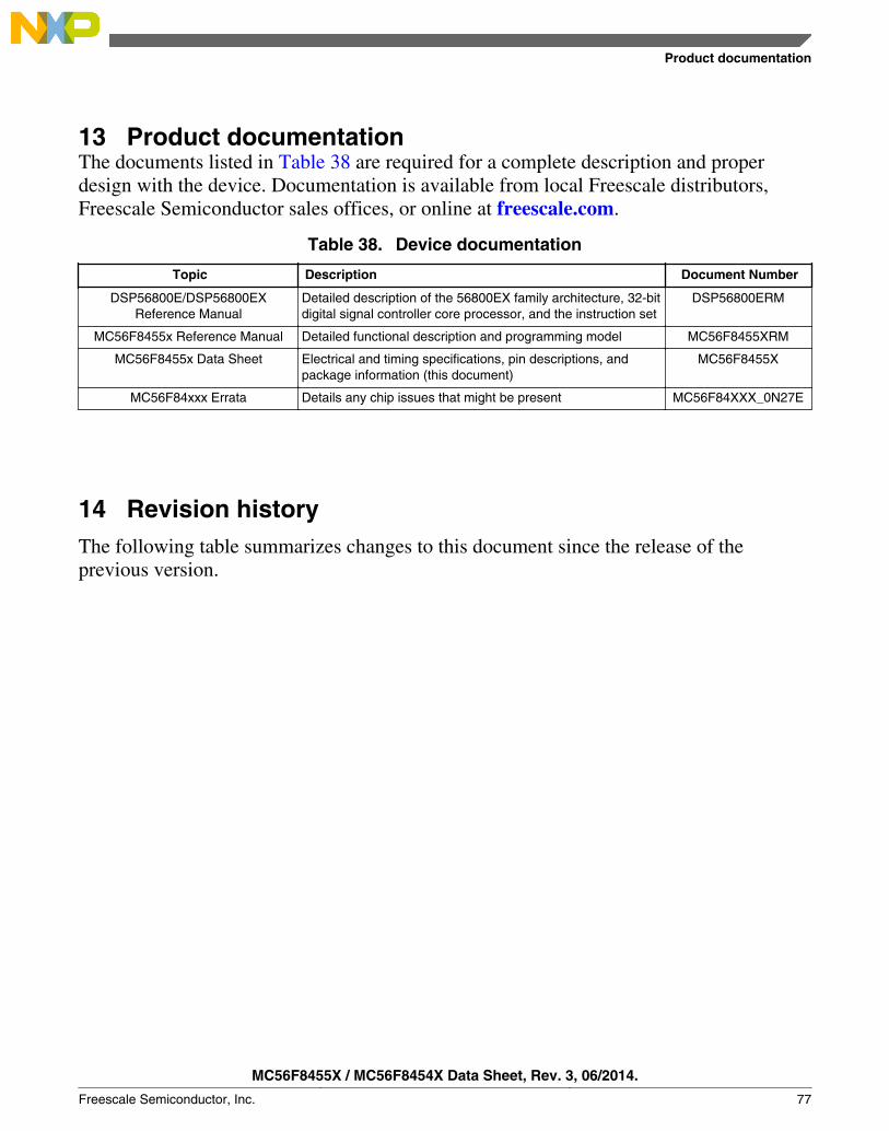
13 Product documentationThe documents listed in Table 38 are required for a complete description and properdesign with the device. Documentation is available from local Freescale distributors,Freescale Semiconductor sales offices, or online at freescale.com.
Table 38. Device documentation
Topic Description Document Number
DSP56800E/DSP56800EXReference Manual
Detailed description of the 56800EX family architecture, 32-bitdigital signal controller core processor, and the instruction set
DSP56800ERM
MC56F8455x Reference Manual Detailed functional description and programming model MC56F8455XRM
MC56F8455x Data Sheet Electrical and timing specifications, pin descriptions, andpackage information (this document)
MC56F8455X
MC56F84xxx Errata Details any chip issues that might be present MC56F84XXX_0N27E
14 Revision historyThe following table summarizes changes to this document since the release of theprevious version.
Product documentation
MC56F8455X / MC56F8454X Data Sheet, Rev. 3, 06/2014.
Freescale Semiconductor, Inc. 77
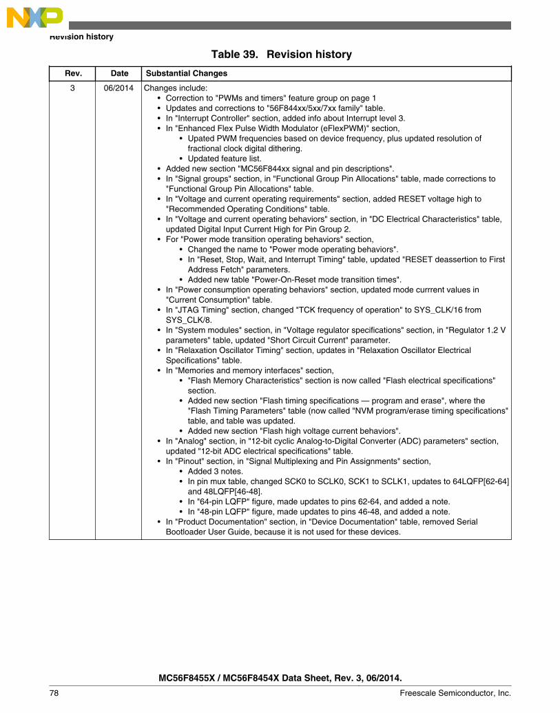
Table 39. Revision history
Rev. Date Substantial Changes
3 06/2014 Changes include:• Correction to "PWMs and timers" feature group on page 1• Updates and corrections to "56F844xx/5xx/7xx family" table.• In "Interrupt Controller" section, added info about Interrupt level 3.• In "Enhanced Flex Pulse Width Modulator (eFlexPWM)" section,
• Upated PWM frequencies based on device frequency, plus updated resolution offractional clock digital dithering.
• Updated feature list.• Added new section "MC56F844xx signal and pin descriptions".• In "Signal groups" section, in "Functional Group Pin Allocations" table, made corrections to
"Functional Group Pin Allocations" table.• In "Voltage and current operating requirements" section, added RESET voltage high to
"Recommended Operating Conditions" table.• In "Voltage and current operating behaviors" section, in "DC Electrical Characteristics" table,
updated Digital Input Current High for Pin Group 2.• For "Power mode transition operating behaviors" section,
• Changed the name to "Power mode operating behaviors".• In "Reset, Stop, Wait, and Interrupt Timing" table, updated "RESET deassertion to First
Address Fetch" parameters.• Added new table "Power-On-Reset mode transition times".
• In "Power consumption operating behaviors" section, updated mode currrent values in"Current Consumption" table.
• In "JTAG Timing" section, changed "TCK frequency of operation" to SYS_CLK/16 fromSYS_CLK/8.
• In "System modules" section, in "Voltage regulator specifications" section, in "Regulator 1.2 Vparameters" table, updated "Short Circuit Current" parameter.
• In "Relaxation Oscillator Timing" section, updates in "Relaxation Oscillator ElectricalSpecifications" table.
• In "Memories and memory interfaces" section,• "Flash Memory Characteristics" section is now called "Flash electrical specifications"
section.• Added new section "Flash timing specifications — program and erase", where the
"Flash Timing Parameters" table (now called "NVM program/erase timing specifications"table, and table was updated.
• Added new section "Flash high voltage current behaviors".• In "Analog" section, in "12-bit cyclic Analog-to-Digital Converter (ADC) parameters" section,
updated "12-bit ADC electrical specifications" table.• In "Pinout" section, in "Signal Multiplexing and Pin Assignments" section,
• Added 3 notes.• In pin mux table, changed SCK0 to SCLK0, SCK1 to SCLK1, updates to 64LQFP[62-64]
and 48LQFP[46-48].• In "64-pin LQFP" figure, made updates to pins 62-64, and added a note.• In "48-pin LQFP" figure, made updates to pins 46-48, and added a note.
• In "Product Documentation" section, in "Device Documentation" table, removed SerialBootloader User Guide, because it is not used for these devices.
Revision history
MC56F8455X / MC56F8454X Data Sheet, Rev. 3, 06/2014.
78 Freescale Semiconductor, Inc.
How to Reach Us:
Home Page:www.freescale.com
Web Support:http://www.freescale.com/support
USA/Europe or Locations Not Listed:Freescale SemiconductorTechnical Information Center, EL5162100 East Elliot RoadTempe, Arizona 85284+1-800-521-6274 or +1-480-768-2130www.freescale.com/support
Europe, Middle East, and Africa:Freescale Halbleiter Deutschland GmbHTechnical Information CenterSchatzbogen 781829 Muenchen, Germany+44 1296 380 456 (English)+46 8 52200080 (English)+49 89 92103 559 (German)+33 1 69 35 48 48 (French)www.freescale.com/support
Japan:Freescale Semiconductor Japan Ltd.HeadquartersARCO Tower 15F1-8-1, Shimo-Meguro, Meguro-ku,Tokyo 153-0064Japan0120 191014 or +81 3 5437 [email protected]
Asia/Pacific:Freescale Semiconductor China Ltd.Exchange Building 23FNo. 118 Jianguo RoadChaoyang DistrictBeijing 100022China+86 10 5879 [email protected]
Document Number: MC56F8455XRev. 3, 06/2014
Information in this document is provided solely to enable system and softwareimplementers to use Freescale Semiconductors products. There are no express or impliedcopyright licenses granted hereunder to design or fabricate any integrated circuits orintegrated circuits based on the information in this document.
Freescale Semiconductor reserves the right to make changes without further notice to anyproducts herein. Freescale Semiconductor makes no warranty, representation, orguarantee regarding the suitability of its products for any particular purpose, nor doesFreescale Semiconductor assume any liability arising out of the application or use of anyproduct or circuit, and specifically disclaims any liability, including without limitationconsequential or incidental damages. "Typical" parameters that may be provided inFreescale Semiconductor data sheets and/or specifications can and do vary in differentapplications and actual performance may vary over time. All operating parameters,including "Typicals", must be validated for each customer application by customer'stechnical experts. Freescale Semiconductor does not convey any license under its patentrights nor the rights of others. Freescale Semiconductor products are not designed,intended, or authorized for use as components in systems intended for surgical implantinto the body, or other applications intended to support or sustain life, or for any otherapplication in which failure of the Freescale Semiconductor product could create asituation where personal injury or death may occur. Should Buyer purchase or useFreescale Semiconductor products for any such unintended or unauthorized application,Buyer shall indemnify Freescale Semiconductor and its officers, employees, subsidiaries,affiliates, and distributors harmless against all claims, costs, damages, and expenses, andreasonable attorney fees arising out of, directly or indirectly, any claim of personal injuryor death associated with such unintended or unauthorized use, even if such claims allegesthat Freescale Semiconductor was negligent regarding the design or manufacture ofthe part.
RoHS-compliant and/or Pb-free versions of Freescale products have the functionality andelectrical characteristics as their non-RoHS-complaint and/or non-Pb-free counterparts.For further information, see http://www.freescale.com or contact your Freescalesales representative.
For information on Freescale's Environmental Products program, go tohttp://www.freescale.com/epp.
Freescale™ and the Freescale logo are trademarks of Freescale Semiconductor, Inc.All other product or service names are the property of their respective owners.
© 2014 Freescale Semiconductor, Inc.