Embed Size (px)
Citation preview

FRACTURE PROPERTIES OF GaAs±AlAs SUPERLATTICES
STUDIED BY ATOMIC FORCE MICROSCOPY AND
SCANNING ELECTRON MICROSCOPY
M. R. CASTELL{, A. HOWIE and D. A. RITCHIE
Cavendish Laboratory, Madingley Road, Cambridge, CB3 0HE, U.K.
(Received 3 July 1997; accepted 10 July 1997)
AbstractÐGaAs±AlAs superlattices with periodicities of up to 200 nm were cleaved to expose (110) faces.These surfaces were studied using high resolution scanning electron microscopy where the secondary elec-tron images reveal contrast between the GaAs and AlAs layers and also indicate that the AlAs layers aretopographically raised with respect to the GaAs. Atomic force microscopy of the same samples shows thatthe AlAs ridges can extend as far as 55 nm beyond the GaAs surface. Further secondary electron imagesof cross-sections of plastically deformed GaAs±AlAs superlattices reveal that the AlAs layers can undergosevere deformation whereas the GaAs layers fracture more readily. It is proposed that the AlAs protrusionson the (110) cleavage surface are due to the fracture behaviour of the superlattice as well as oxidatione�ects. # 1998 Acta Metallurgica Inc.
1. INTRODUCTION
The unique electronic and optical properties of low
dimensional structures has resulted in extensive stu-
dies of their microstructure. Quantum con®nement
e�ects can be correlated with the quality of the
interfaces and uniformity of the layers as deter-
mined by transmission electron microscopy, sputter
assisted evaluation, or optical methods. Surface sen-
sitive microscopy such as atomic force microscopy
(AFM) is also extensively used, but this relies on
the creation of a ¯at cross-section through the
quantum well region. This can be readily achieved
on most III±V semiconductors as they cleave with
relative ease on (110) planes. Previous reports on
scanning probe microscopy studies of (110) cross-
sections through GaAs±AlGaAs [1±4] and
GaInAs±InP [5±7] superlattices have revealed that,
even without chemical etching, corrugations with
the superlattice periodicity are seen. The corruga-
tion height is generally of the order of less than a
nanometre and has been attributed to either di�er-
ences in the electronic properties of the quantum
wells a�ecting scanning tunnelling microscope
(STM) imaging [5, 6] or preferential oxidation of
one of the phases giving rise to topograpical
di�erences [1, 3, 4, 6].
The only mention that the corrugations might be
due to the cleavage process itself was rejected by
Kato et al. [5] on the grounds that both cleavage
surfaces were mirror images of each other, which is
also in agreement with the observations presentedin this paper. Kato et al. state that a cleavage arte-fact should result in the two opposite faces being
inverses of each other. In their view, the experimen-tal observation of the mirror image faces is incon-sistent with a cleavage artefact. However, here weshow that during cleavage of GaAs±AlAs superlat-
tices the GaAs layers fracture readily whereas theAlAs layers deform plastically before fracture,resulting in AlAs protrusions on both cleavage sur-
faces with heights of up to 55 nm.
2. EXPERIMENTAL PROCEDURE
The GaAs±AlAs superlattices used in the exper-iments were grown in a VG Semicon V80H molecu-lar beam epitaxy (MBE) system on (001) GaAssubstrates. Cross-sectional cleavage exposing a
(110) surface was peformed in air and within halfan hour the samples were introduced into the vac-uum chamber of a Hitachi S900 scanning electron
microscope (SEM). The immersion lens geometryand ®eld emission gun of this microscope makesub-nanometre resolution possible in secondary
electron (SE) imaging mode. The SE images pre-sented in this paper were all taken using primaryelectrons with energies of 20 keV or 25 keV. The
topography of cleavage surfaces of samples (pre-pared in the same way as for the SEM experiments)was investigated in ambient conditions with aNanoscope II AFM using microfabricated Si tips.
Acta mater. Vol. 46, No. 2, pp. 579±584, 1998# 1998 Acta Metallurgica Inc.
Published by Elsevier Science Ltd. All rights reservedPrinted in Great Britain
1359-6454/98 $19.00+0.00PII: S1359-6454(97)00242-5
{To whom all correspondence should be addressed.Present address: Department of Materials, Universityof Oxford, Parks Road, Oxford OX1 3PH, U.K..
579

3. RESULTS AND DISCUSSION
Figure 1 shows corresponding AFM and SEM
images, as well as AFM linetraces, of the (110) clea-
vage surface of three GaAs±AlAs superlattices. The
SEM images were taken at 20 keV in the SE ima-
ging mode. The SE contrast across the layers in
Fig. 1(a) can be explained as follows. The light grey
regions are GaAs, and the dark layers are AlAs,
which is due to the greater SE emission coe�cient
of GaAs compared with AlAs [8±10]. The layer
widths measured from the micrograph are 90 nm
and 109 nm for the AlAs and GaAs layers respect-
ively. At the edges of the AlAs layers the image
appears bright owing to the increased SE signal at
abrupt changes in topography [11]. The bright ridge
indicates the top of a step and is accompanied by a
dark region next to it where SE emission at the bot-
tom of the step is reduced. At the irregular (right
hand) side of the AlAs layers, the dark region is
highly pronounced which indicates the presence of
a deep cavity, presumably caused by delamination
of the layer. This delamination is only present on
one side of the layers but can occur on both sides
as shown in Fig. 1(d).
The sample topography of Fig. 1(a), as imaged
by AFM, is shown in Fig. 1(b). It is immediately
apparent that the image has been adversely a�ected
by the shape of the probe tip. Where one would
expect a trace of approximately the form of a
square wave, the linetrace in Fig. 1(c) shows that
during scanning the AFM tip only just reaches the
bottom of the troughs between the AlAs ridges.
Although the AFM data cannot be viewed as an
accurate representation of the true surface topogra-
phy, it contains reliable information on the period-
icity of the superlattice and the height of the AlAs
ridges. The periodicity was measured to be 200
nm26 nm, which may be compared with 199
nm28 nm determined from the SE micrograph in
Fig. 1(a). The AlAs ridge heights were found to be
Fig. 1. Secondary electron (a,d,g) and atomic force microscope (b,e,h) images of (110) cleavage surfacesof GaAs±AlAs superlattices of di�ering layer thicknesses. In the SE images (a,d) taken at 20 keV, theGaAs and AlAs layers appear bright and dark, respectively, and are separated by dark±light doublets.In the SE image in (g) the AlAs layers appear bright owing to their topography. The surface imaged byAFM shows that the AlAs layers have formed ridges of 55 nm, 45 nm, and 4 nm heights in images b,e, and h, respectively. Typical AFM linescans perpendicular to the layers are shown in parts c, f, and i.
All image widths are 1 mm.
CASTELL et al.: FRACTURE PROPERTIES OF SUPERLATTICES580
surprisingly large at 55 nm23 nm, as can be seen
in Fig. 1(c).
The lack of variation of the SE contrast across
the GaAs layers at the bottom of the troughs indi-
cates that the SE signal contributing to the image is
highly localized. The contrast between the GaAs
and AlAs layers must therefore be due mainly to
two e�ects. Firstly, the di�erences in stopping
power between the materials (GaAs has a higher
stopping power than AlAs). This will give rise to
greater SE emission at the beam entrance point in
GaAs relative to AlAs. Secondly, the additional
SEs that are created in the higher atomic number
material (GaAs) when high angle elastically back-
scattered electrons exit the material [10].
Figure 1(d) shows an image of a GaAs±AlAs
superlattice grown to di�erent speci®cations from
the one discussed above. The SE micrograph in
Fig. 1(d) reveals that the dark AlAs layers are sig-
ni®cantly thicker than the bright GaAs layers, and
®ne dark±bright doublets can be seen at the steps
between the layers. In this micrograph delamination
between the layers is more clearly pronounced than
in Fig. 1(a). The superlattice periodicity measured
from the SE micrograph is 108 nm24 nm, com-
pared with a value of 111 nm23 nm determined
by AFM [Fig. 1(e)]. As the troughs between the
AlAs ridges are 26 nm22 nm, i.e. narrower than in
the sample shown on Fig. 1(b), the AFM tip only
indicates the presence of the troughs and is not able
to image their true depth. However, the AlAs ridge
height of 45 nm22 nm may be determined by
measuring the height of the left most AlAs ridge, as
seen in the linescan in Fig. 1(f).
The SE image of a GaAs±AlAs superlattice con-
sisting mainly of GaAs is shown in Fig. 1(g). The
sample was cleaved to expose the superlattice which
consists of 8.6 nm20.5 nm AlAs layers and 97.8nm23 nm GaAs layers, as determined using
growth-rate data and X-ray di�raction. As was the
case with the previous GaAs±AlAs superlattices,
the AlAs layers formed ridges, but in this case thewidth of the layers is so small that the high SE
yield at either side of the ridge causes the whole
ridge to appear brighter than the GaAs. The AlAs
ridges therefore appear bright owing to topographic
contrast, which more than o�sets the low SE yieldfrom AlAs compared with GaAs. The superlattice
periodicity, measured from the SE micrograph and
AFM data [Fig. 1(h)] was 111 nm23 nm and the
AlAs ridge height was 4 nm20.5 nm, as seen inthe AFM linescan in Fig. 1(i).
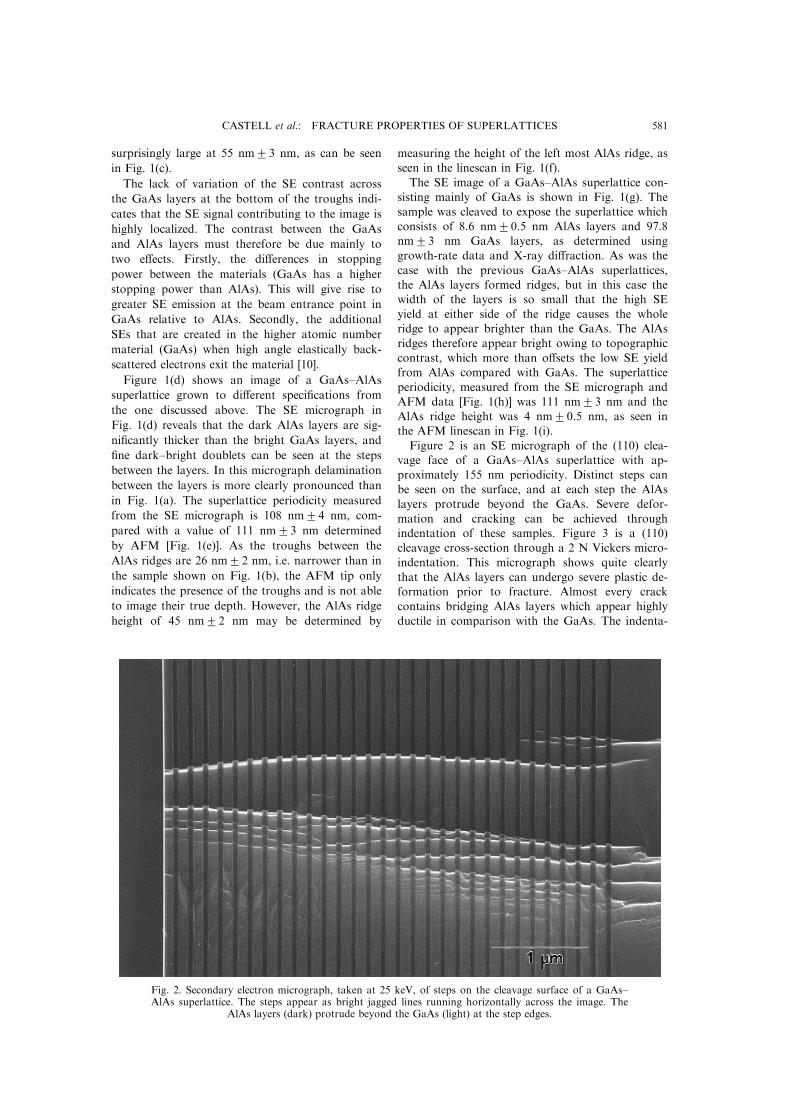
Figure 2 is an SE micrograph of the (110) clea-vage face of a GaAs±AlAs superlattice with ap-
proximately 155 nm periodicity. Distinct steps can
be seen on the surface, and at each step the AlAs
layers protrude beyond the GaAs. Severe defor-
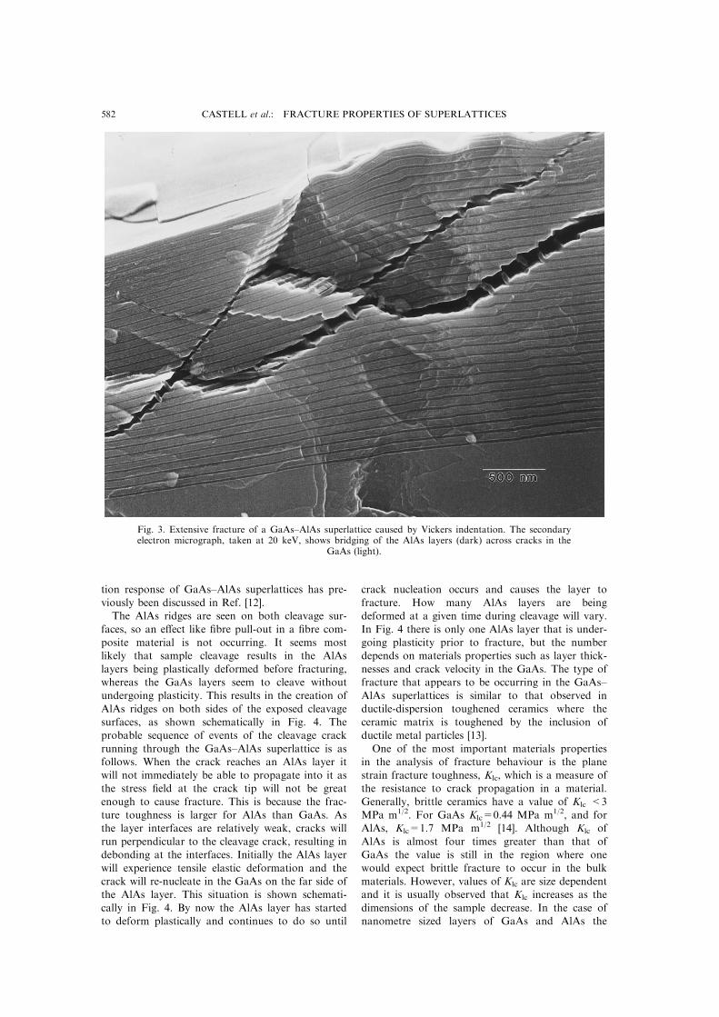
mation and cracking can be achieved throughindentation of these samples. Figure 3 is a (110)
cleavage cross-section through a 2 N Vickers micro-
indentation. This micrograph shows quite clearly
that the AlAs layers can undergo severe plastic de-formation prior to fracture. Almost every crack
contains bridging AlAs layers which appear highly
ductile in comparison with the GaAs. The indenta-
Fig. 2. Secondary electron micrograph, taken at 25 keV, of steps on the cleavage surface of a GaAs±AlAs superlattice. The steps appear as bright jagged lines running horizontally across the image. The
AlAs layers (dark) protrude beyond the GaAs (light) at the step edges.
CASTELL et al.: FRACTURE PROPERTIES OF SUPERLATTICES 581
tion response of GaAs±AlAs superlattices has pre-
viously been discussed in Ref. [12].The AlAs ridges are seen on both cleavage sur-
faces, so an e�ect like ®bre pull-out in a ®bre com-
posite material is not occurring. It seems mostlikely that sample cleavage results in the AlAs
layers being plastically deformed before fracturing,whereas the GaAs layers seem to cleave without
undergoing plasticity. This results in the creation of
AlAs ridges on both sides of the exposed cleavagesurfaces, as shown schematically in Fig. 4. The
probable sequence of events of the cleavage crack
running through the GaAs±AlAs superlattice is asfollows. When the crack reaches an AlAs layer it
will not immediately be able to propagate into it asthe stress ®eld at the crack tip will not be great
enough to cause fracture. This is because the frac-
ture toughness is larger for AlAs than GaAs. Asthe layer interfaces are relatively weak, cracks will
run perpendicular to the cleavage crack, resulting indebonding at the interfaces. Initially the AlAs layer
will experience tensile elastic deformation and the
crack will re-nucleate in the GaAs on the far side ofthe AlAs layer. This situation is shown schemati-
cally in Fig. 4. By now the AlAs layer has startedto deform plastically and continues to do so until
crack nucleation occurs and causes the layer to
fracture. How many AlAs layers are beingdeformed at a given time during cleavage will vary.
In Fig. 4 there is only one AlAs layer that is under-going plasticity prior to fracture, but the number
depends on materials properties such as layer thick-
nesses and crack velocity in the GaAs. The type offracture that appears to be occurring in the GaAs±
AlAs superlattices is similar to that observed inductile-dispersion toughened ceramics where the
ceramic matrix is toughened by the inclusion of
ductile metal particles [13].
One of the most important materials propertiesin the analysis of fracture behaviour is the plane
strain fracture toughness, Klc, which is a measure ofthe resistance to crack propagation in a material.
Generally, brittle ceramics have a value of Klc <3
MPa m1/2. For GaAs Klc=0.44 MPa m1/2, and forAlAs, Klc=1.7 MPa m1/2 [14]. Although Klc of
AlAs is almost four times greater than that ofGaAs the value is still in the region where one
would expect brittle fracture to occur in the bulk
materials. However, values of Klc are size dependentand it is usually observed that Klc increases as the
dimensions of the sample decrease. In the case ofnanometre sized layers of GaAs and AlAs the
Fig. 3. Extensive fracture of a GaAs±AlAs superlattice caused by Vickers indentation. The secondaryelectron micrograph, taken at 20 keV, shows bridging of the AlAs layers (dark) across cracks in the
GaAs (light).
CASTELL et al.: FRACTURE PROPERTIES OF SUPERLATTICES582

values of Klc are certain to be much greater thanfor the bulk materials. As can be seen in the sche-matic diagram of the fracture process (Fig. 4), the
layered nature of the material and the interfacesbetween the layers both play an important role. Thetype of cleavage mechanism discussed above isentirely di�erent from the situation in a bulk
sample of GaAs or AlAs. As the crack propagatesthrough the superlattice there are continuous crackre-nucleation events as well as plastic deformation
of the AlAs layers. This means that the fracturetoughness of one of these types of superlatticeshould be signi®cantly greater than the average of
its components. Size dependent e�ects are com-monly observed in fracture mechanics and couldexplain why AlAs in a layered form behaves di�er-ently from the bulk material.
4. CONCLUSION
We have shown that cleavage of GaAs±AlAs
superlattices results in the creation of AlAs ridgesformed by plastic deformation of the AlAs layersduring fracture. Previous observations of small cor-
rugations (less than a nanometre) observed oncleaved AlGaAs±GaAs superlattices were mostlikely correctly attributed to preferential AlGaAs
oxide formation, but the results on GaAs±AlAssuperlattices presented here show that larger corru-gation amplitudes are mainly due to AlAs layer
plasticity. We have carried out similar experimentsto those described above on a variable compositionGaAs-superlattice and have not observed this unu-sual fracture behaviour. As can be seen in the SE
images, the ridges have an almost rectangular cross-section and can be as high as 55 nm. If the ridgeswere oxide, one would expect them to have grown
in a far more di�use shape than the images suggest,and it is unlikely that the ridges could have attaineda height of 55 nm. Conclusive evidence of AlAsplasticity is provided by the images of the deformed
superlattices which show plastically elongated AlAslayers bridging cracks in the GaAs matrix.It is possible that the type of GaAs±AlAs super-
lattices described in this paper could be incorpor-ated into GaAs-based electronic devices that areprone to fracture. The ductile behaviour of the
AlAs layers increases the fracture toughness of thematerial and causes reduced crack propagation per-pendicular to the layers.
AcknowledgementsÐWe are grateful to Dr D.A. Williamsof the Hitachi Cambridge Laboratory who rendered valu-able assistance in the SEM operation which was gener-ously donated to the Cavendish Laboratory by HitachiLtd. We would also like to thank the EPSRC for fundingthe Cambridge MBE programme and the CASE student-ship for MRC who was also supported by the NationalPhysical Laboratory.
REFERENCES
1. Prohaska, T., Friedbacher, G., Grasserbauer, M.,Nickel, H., LoÈ sch, R. and Schlapp, W., Anal. Chem.,1995, 67, 1530.
2. Gwo, S., Chao, K-J. and Shih, C. K., Appl. Phys.Lett., 1994, 64, 493.
3. Friedbacher, G., Hansma, P. K., Schwarzbach, D.,Grasserbauer, M. and Nickel, H., Anal. Chem., 1992,64, 1760.
Fig. 4. Schematic illustration of the cleavage of a GaAs±AlAs superlattice. As the crack propagates theAlAs layers are plastically deformed prior to fracture resulting in a series of AlAs ridges on both clea-
vage faces.
CASTELL et al.: FRACTURE PROPERTIES OF SUPERLATTICES 583
4. Chalmers, S. A., Gossard, A. C., Weisenhorn, A. L.,Gould, S. A. C., Drake, B. and Hansma, P. K.,Appl. Phys. Lett., 1989, 55, 2491.
5. Kato, T., Osaka, F. and Tanaka, I., Jap. J. Appl.Phys., 1989, 28, 1050.
6. Howells, S., Gallagher, M. J., Chen, T., Pax, P. andSarid, D., Appl. Phys. Lett., 1992, 61, 801.
7. Tamayo, J. and Garcia, R., Mater. Sci. Engng, 1996,B42, 122.
8. Bleloch, A. L., Castell, M. R., Howie, A. and Walsh,C. A., Ultramicroscopy, 1994, 54, 107.
9. Perovic, D. D., Castell, M. R., Howie, A., Lavoie,C., Tiedje, T. and Cole, J. S. W., Ultramicroscopy,1995, 58, 104.
10. Merli, P. G., Migliori, A., Nacucchi, M., Govoni, D.
Mattei, G., Ultramicroscopy, 1995, 60, 229.
11. Reimer L., Scanning Electron Microscopy. Springer
Series in Optical Sciences, Springer Verlag, Berlin,
Vol. 45.
12. Castell, M. R., Howie, A., Perovic, D. D., Ritchie,
D. A., Churchill, A. C. and Jones, G. A. C., Phil.
Mag. Lett., 1993, 67, 89.
13. Lawn B., Fracture of Brittle SolidsÐSecond Edition.
Cambridge University Press, Cambridge, 1993.
14. Hjort, K., SoÈ derkvist, J. and Schweitz, J.-AÊ .,
J. Mircomech. Microengng, 1994, 4, 1.
CASTELL et al.: FRACTURE PROPERTIES OF SUPERLATTICES584